
Realization of a quantum Hamiltonian Boolean logic gate on the Si(001):H surface†
Marek
Kolmer
a,
Rafal
Zuzak
a,
Ghassen
Dridi
b,
Szymon
Godlewski
*a,
Christian
Joachim
bc and
Marek
Szymonski
a
aCentre for Nanometer-Scale Science and Advanced Materials, NANOSAM, Faculty of Physics, Astronomy and Applied Computer Science, Jagiellonian University, Lojasiewicza 11, 30-348 Krakow, Poland. E-mail: szymon.godlewski@uj.edu.pl
bNanosciences Group & MANA Satellite, CEMES-CNRS, 29 rue Jeanne Marvig, F-31055 Toulouse, France
cInternational Center for Materials Nanoarchitectonics (MANA), National Institute for Materials Science (NIMS), 1-1 Namiki, Tsukuba, Ibaraki 305-0044, Japan
First published on 24th June 2015
Abstract
The design and construction of the first prototypical QHC (Quantum Hamiltonian Computing) atomic scale Boolean logic gate is reported using scanning tunnelling microscope (STM) tip-induced atom manipulation on an Si(001):H surface. The NOR/OR gate truth table was confirmed by dI/dU STS (Scanning Tunnelling Spectroscopy) tracking how the surface states of the QHC quantum circuit on the Si(001):H surface are shifted according to the input logical status.
Continuous miniaturization of electronic circuits results in the nanometer-scale design of modern devices and integrated circuits engraved on the surface of a semiconductor solid. Nowadays, the development of integrated electronic circuits has approached size limitations due to quantum effects affecting the circuit's performance.1 The continuation of this miniaturization requires alternative approaches as compared with solid state devices. The utilization of a single molecule per device in an electronic circuit2 is regarded as one of the most challenging and promising approaches.3 Experiments on single organic molecule(s) in prototypical electronic devices became feasible after the invention of the scanning tunnelling microscope (STM),4,5 enabling structural and electronic characterization as well as the atomically precise construction of atomic and molecular devices.6–8 Many experiments have been performed to characterize single molecule properties and the operation of a simple molecule logic gate was demonstrated9 even using a molecule cascade design.10 However, most of these experiments were conducted on a metal surface. Such a surface is not very practical for single molecule device studies since the intermixing of molecule and substrate quantum electronic states strongly modifies the way the prototypical device performs. Therefore, the possibility of providing sufficient electronic decoupling of the molecule from the surface started to be explored and this isolation can be achieved when an ultra-thin insulating layer is covering the metal surface.11,12 More recently, it has been demonstrated that a semiconductor surface passivated by a hydrogen layer can also electronically isolate the adsorbed molecule from the semiconductor substrate.13–16 For example, hydrogen passivated silicon13 and germanium15 surfaces provide an efficient isolation of adsorbed molecules and preserve their intrinsic electronic properties. However, calculations have demonstrated that the electronic contact between the active molecules with the circuit to perform Boolean logic operations and the interconnects with the users may suppress the device performance.17 Therefore to avoid such a hybrid approach, a new solution had been proposed based on the use of surface atomic circuits constructed with surface dangling bonds (DBs) created for example upon atom by atom hydrogen desorption.17–24 The application of selective highly doped dehydrogenated nanostructures was also proposed.25–27 All these electronic circuits can effectively be constructed with atomic precision using the STM ability for vertical atom by atom manipulation.23,28,29 To go further into the miniaturisation of atomic scale circuits and also to benefit from surface quantum state behaviour, we present in this letter the realization of the first prototype of a planar QHC (Quantum Hamiltonian Computing) Boolean logic gate constructed at the atomic scale on a Si(001):H surface. Formally, the QHC approach does not need a sub-division of the quantum system into qubits and is based on the control of the energy position and of the nodal spatial structure of the eigenstates of a given H0 calculating Hamiltonian by performing local changes on very specific elements of its matrix to input classical logical information. For well-designed QHC Hamiltonians, the spectral displacement of well identified H0 eigenstates follows a Boolean truth table according to the input logical status.30,31
The experiments were carried out in a multi-chamber ultra-high vacuum (UHV) system with a base pressure in the low 10−10 mbar range. The scanning tunnelling microscopy/spectroscopy (STM/STS) measurements were performed using an Omicron GmbH low-temperature STM machine operating at cryogenic temperatures of 4.5 K (liquid helium) and 77 K (liquid nitrogen) with electrochemically etched tungsten tips used as probes. A single dI/dU spectrum was obtained by differentiating several I(U) curves collected for a particular STM tip location. In the present study we have used the hydrogenated Si(001)-(2 × 1):H surface prepared using two different methods on slightly B doped p-type single crystal samples with the nominal doping density reaching approximately 1015–1016 cm−3. First, the samples were cut from commercially available Si(001) wafers (TBL Kelpin Crystals) and treated by the standard UHV surface preparation including cycles of direct current heating followed by surface hydrogenation.32 Second, we cleaved in situ under UHV conditions the samples provided by CEA-LETI Grenoble.24 Both preparation procedures result in perfectly reconstructed Si(001)-(2 × 1):H surfaces with single, atomic scale defects, mainly in the form of native DBs. Our STM/STS data show coherent results on both types of samples. The Heisenberg–Rabi oscillations were calculated by solving numerically the time dependent Schrodinger equation.†
The electronic structure of a QHC logic gate depends on the symmetry of the quantum system used and practically chosen to encode the logical inputs.33 In this work and for a Si(001):H surface, the electronic structure of a QHC logic gate is constructed atom by atom by creating dangling bond dimers (DBDs) along a single dimer row. In order to introduce moderate electronic interactions through the surface between the created DBDs, we have chosen to spatially separate the active DBDs of the structure by keeping 2 passivated Si dimers along the same row as presented in Fig. 1a. The (α,β) logical inputs are defined by attributing a logical “0” when there is no hydrogen atom on the input DBD and a logical “1” when two hydrogen atoms are saturating the input DBD (the reverse can be equally chosen leading to the dual AND/NAND Boolean logic gate). As presented in Fig. 1a, the two DBD inputs are positioned laterally and on different surface dimer rows as compared to the 3 other DBDs. For such a surface structure, the functioning of the NOR/OR QHC logic gate can be easily simulated by constructing the corresponding simple 10 quantum state Hamiltonian model system as presented in Fig. 1b with its corresponding 10 × 10 H0(α,β) Hamiltonian matrix (Fig. 1c). The H0(α,β) matrix elements are given in the caption of Fig. 1. Their order of magnitude was estimated using our previous studies on Si(001):H semi-classical electronic circuits.18 Experimentally, the gate performance was analysed using STS measurements by placing the tip centrally over the structure as schematically shown in Fig. 1d. The functioning of the NOR/OR Boolean logic gate can also be easily verified mathematically by tracking the H0(α,β) eigenstates reaching the NOR and OR reference energies depending on the logical inputs, attributing a logical “1” output in this case as presented in Fig. 1e. To characterize simply the logical output status of a QHC logic gate, a quantum “reading head” made of two |Φa〉 and |Φb〉 degenerate states is usually added to the H0(α,β) in Fig. 1 leading to the quantum system in Fig. 2a and to the corresponding 12 × 12 H(α,β) matrix presented in Fig. 2b. This quantum system can oscillate in time between |Φa〉 and |Φb〉 through the 10 × 10 H0(α,β) quantum system when one electronically coupled H0(α,β) eigenstate is resonating with |Φa〉 and |Φb〉. Starting at t = 0 from |Φa〉, we have calculated the |〈Φb|ψ(t)〉|2 Heisenberg–Rabi oscillations for the 2 different NOR and OR output reference energies and for all four (α,β) logical input configurations. With the H0(α,β) matrix elements in Fig. 1 and as presented in Fig. 2d and e, the NOR and OR gates are working perfectly since for the (α,β) input configurations leading to a logical output “1” (i.e. a fast Heisenberg–Rabi oscillations), at least one of the H0(α,β) eigenstates is resonating with |Φa〉 and |Φb〉 as presented in Fig. 1e. These time dependent Heisenberg–Rabi oscillations are too fast to be experimentally recorded in time. But they are very useful in the optimization of H0(α,β) of a given QHC gate. Then, after the optimization, the electronic coupling between |Φa〉 and |Φb〉 to a 2 atomic scale DB wire as presented in Fig. 2c opens a practical way to measure this oscillation frequency since the tunnelling current intensity between |Φa〉 and |Φb〉 through the QHC logic gate in Fig. 1 is proportional to the square of this frequency.34 In the absence of planar atomic scale interconnects shown in Fig. 2c, that would allow a planar current intensity measurement, the output status of the QHC logic gate in Fig. 1 was determined here, by locating the STM tip apex at the centre of the DBD gate structure, as already presented in Fig. 1d. Subsequently the STS dI/dU electronic spectra were recorded to follow how the surface states of this quantum circuit are shifted in energy according to the DBD binary inputs.
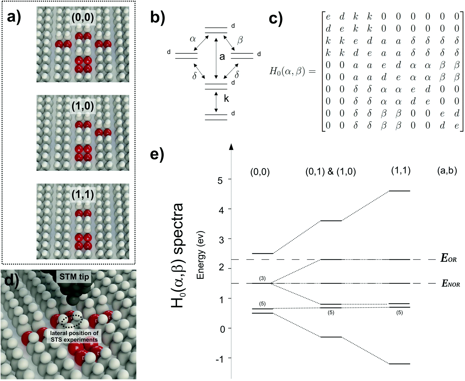 | ||
| Fig. 1 (a) Schematic representation of a QHC NOR/OR Boolean logic gate implanted on the Si(001):H surface. Grey and red balls depict hydrogenated and bare silicon atoms, respectively. (b) The oversimplified quantum graph simulating the functioning of the QHC NOR/OR Si(001):H planar logic gate presented in (a). (c) The 10 × 10 H0(α,β) matrix of the QHC gate in (b) with its logical inputs (α,β). The H0(α,β) matrix elements are: a = 0.255 eV, d = 0.455 eV, k = 0.4 eV, δ = 0.04 eV and e = 1.1 eV (see ref. 18 for the estimation of the values). The logical inputs (α,β) were attributed the values 0.0 eV and 1.0 eV to enhance the spectral functioning of the gate leading to a large level repulsion effect represented in (e). (d) The STS dI/dU experimental configuration with the STS tip apex positioned at the vertical output of the gate for recording the position of the electronic resonance of this tunnelling junction as a function of the DBD logical input configurations. (e) The variation in energy of the H0(α,β) Hamiltonian eigenvalues in (c) as a function of the logical inputs. The logical output reference energies are 1.55 eV for the NOR and 2.315 eV for the OR relative to e = 1.1 eV. The multiplicity of the H0(α,β) eigenstates is indicated in parenthesis. Notice that for (0,1), (1,0) and (1,1) logical input configurations, the remaining H0(α,β) eigenstate located at 1.55 eV is not playing any role. | ||
 | ||
| Fig. 2 (a) The simplified quantum system including the NOR/OR calculating QHC circuit defined in Fig. 1b and the |Φa〉 and |Φb〉 output reading states of energy ENOR = 1.55 eV and EOR = 2.315 eV. (b) The 12 × 12 H(α,β) matrix of the quantum system in (a) including the 2 × 2 reading block at the reference energy E and the 10 × 10 H0(α,β) calculating matrix. The ε coupling matrix element is controlling the overall order of magnitude of the Heisenberg–Rabi oscillation frequency. Values up to 0.01 eV still preserve the spectral functioning of this QHC gate. (c) The planar implantation of the NOR/OR QHC logic gate with its DB surface atomic wire in charge of measuring the Heisenberg–Rabi oscillation frequency via the tunneling current intensity passing through the gate. (d, e) The results of the exact |〈Φb|ψ(t)〉 |2 calculations solving the time dependent Schrödinger equation starting at t = 0 from the |Φa〉 non-stationary state. The NOR Heisenberg–Rabi oscillations were calculated at the NOR reference output energy E = 1.55 eV and the OR ones at the OR output reference energy E = 2.315 eV for small ε = 0.001 eV electronic coupling with the |Φa〉 and |Φb〉 output reading states. For this ε value, the NOR logical “1” effective output frequency is 54 GHz and the OR one between 64 GHz and 95 GHz. The “0” NOR and OR output frequencies are all lower than 2 GHz giving a large “0” to “1” margin for measuring the tunnelling current intensity passing through this gate. | ||
The practical construction of the selected QHC surface atomic circuits has been done following the appropriate STM tip-induced desorption protocols obtained in our previous work.22–24 The construction of the DB gate was performed by a multistep sequential procedure involving subsequent extraction of individual DBs. The removal of a single hydrogen atom was achieved by placing the STM tip over the selected H atom with the filled state imaging settings (−2.0 V). Afterwards the feedback loop was switched off, the voltage was switched to positive values and raised to the range of 2.5–3.5 V and the hydrogen desorption was recorded as a sudden rise in the tunnelling current as described in ref. 24. This procedure was repeated step by step until the desired surface circuit was manufactured. The sequential construction of the surface structure is presented in Fig. 3. It is worth noting that the filled state STM image of the DBD shows the protrusion located symmetrically over the hydrogenated surface rows (see the left panel of Fig. 3a). When the second DBD is extracted the lobe becomes more oval and elongated along the direction of the surface rows (the left panel of Fig. 3b). The empty state STM images exhibit a remarkably different appearance.
 | ||
| Fig. 3 Series of LT-STM images presenting results of tip-induced desorption of single H atoms from the Si(001)-(2 × 1):H surface performed at 4.5 K. (a) Singe DB dimer, 5 nm × 3.5 nm. (b) Two DB dimers in parallel configuration, 5.5 nm × 3.5 nm. (c) Three DB dimers forming the (1,1) input state of the QHC gate, 6 nm × 3.5 nm. STM scanning parameters: 10 pA, −2 V for the left column and 10 pA, +2 V for the right column. Structural models of presented structures are also shown. Grey and red balls depict hydrogenated and bare silicon atoms, respectively. | ||
The single DBD is observed as two bright bumps located symmetrically over the hydrogenated row with the additional elongated feature of much lower intensity lying between the bright spots forming a butterfly-like motif (the central panel of Fig. 3a). Extraction of the neighbouring DBD leads to the elongation of the structure image, but the presence of the two side lobes and the additional central one is still preserved (the central panel of Fig. 3b). This provides clear differentiation from single DBs allowing for unambiguous assignment of the constructed atomic structures and has been described in detail previously.24
Following the quantum design in Fig. 1 and applying the desorption procedure, we have constructed the surface logic gate as shown in Fig. 4a. The main part of the gate contains three DB dimers extracted within the same surface reconstruction row. The logical input is provided by the additional surface dimers located on neighbouring surface rows on both sides of the gate backbone. Switching between the logical input “1” and “0” on a given input is achieved by desorption of the two hydrogen atoms of the same dimer. It is worth noting that the reversed switching may be realized for example by the application of the procedure introduced by Labidi et al.35 Manipulating a single molecule on (or out of) the specific DB dimer is also a very attractive possibility to secure one logical input in a bi-stable way.36 The functioning of the constructed gate was tested by performing the spectroscopy measurements with the tip placed over the central part of the gate as shown in Fig. 4a.
 | ||
| Fig. 4 (a) Dangling bond NOR/OR logic gates on an Si(001)-(2 × 1):H surface at 4.5 K. The logical inputs for the different structures of the gate are given on the left side of the STM images (3.5 nm × 3 nm). STM scanning parameters are: −2 V, 10 pA (left column) and +2 V, 10 pA (right column). Structural models of QHC logic gate structures are also shown. Grey and red balls depict hydrogenated and bare silicon atoms, respectively, slight asymmetry seen in the empty state image of the (0,0) input configuration comes from the tip modification resulting from hydrogen atoms captured during gate fabrication. (b) STS dI/dU measurements for different logic gate inputs recorded at 4.5 K over the central part of the gate, solid lines show the averaged data, whereas dashed curves show the data prior to averaging (see elliptical dashed lines in structural models in (a)). | ||
To provide a reliable comparison, the tip was positioned at the same location for all the experiments, testing the influence of the input dimers on the logic gate logical answer. The resulting dI/dU spectrum of the NOR/OR logic gate function is shown in Fig. 4b. Notice that the experimental realization of the gate performance was performed with tunnelling currents limited to several tens of pA due to relatively poor sample conductivity at 4.5 K. Therefore, to provide additional validation of the spectroscopic results, we have constructed and subsequently characterized spectroscopically the gate also at liquid nitrogen temperature. The results obtained with higher tunnelling currents are fully consistent with the ones recorded at liquid helium and are presented in ESI Fig. S1.† The dI/dU spectra obtained for structures of the gate encoded by logical input values “11” and “00” are distinctly different in the vicinity of the empty state resonances. Whereas for “11” and “10” the peak around +1.7 V is observed, for the “00” input configuration, a new tunnelling resonance appears at +1.6 V and the previous one disappears. No important changes were observed around the valence band edge even after approaching the tip towards the surface. Superimposing all STS curves recorded for all input values of the gate in the same figure allows one to follow the displacement in energy of the surface state resonances as a function of the logical input status. As designed, the atomic scale structure is following a NOR logical truth table at +1.6 V. At the same time and from a spectral point of view, this gate structure is also performing like an OR gate for a +1.7 V as predicted theoretically and presented in Fig. 1e.
Conclusions
We showed the first prototypical QHC atomic Boolean logic gate constructed and characterized by LT-STM on the hydrogenated silicon surface. Moreover we successfully measured the truth table of the QHC DB surface logic gate following the theoretical design that is the controlled shift of the surface quantum states following a given Boolean truth table. The gate shows a NOR/OR behaviour in a spectral output mode and at 2 different output energies. The experiments show that the replacement of molecules performing logic functions by atomic circuits is feasible and provides the prospective way to overcome difficulties with the molecule–electrode junction strongly influencing the molecular device performance. According to QHC design rules followed to design the presented NOR/OR gate, more complex logic functions will result from the construction of larger QHC Hamiltonian avoiding the cascading of elementary QHC logic gates by classical electrical wiring. This opens up a new area to incorporate surface atomic logic gates into the more complex circuits leading to the construction of atomic scale devices.Acknowledgements
This research was supported by the 7th Framework Program of the European Union Collaborative Project ICT (Information and Communication Technologies) “Atomic Scale and Single Molecule Logic Gate Technologies” (ATMOL), contract number: FP7-270028. The experiment was carried out using equipment purchased with financial support from the European Regional Development Fund within the framework of the Polish Innovation Economy Operational Program (contract no. POIG.02.01.00-12-023/08). M.K. acknowledges financial support received from the Polish National Science Centre for preparation of his PhD dissertation (decision number: DEC-2013/08/T/ST3/00047) and from the Foundation for Polish Science (FNP).Notes and references
- ITRS Roadmap, 2013 edition, available from http://public.itrs.net.
- A. Aviram and M. A. Ratner, Chem. Phys. Lett., 1974, 29, 277 CrossRef CAS
.
- C. Joachim, J. K. Gimzewski and A. Aviram, Nature, 2000, 408, 541 CrossRef CAS PubMed
- G. Binnig, H. Rohrer, C. Gerber and E. Weibel, Phys. Rev. Lett., 1982, 49, 57 CrossRef
- G. Binnig and H. Rohrer, Rev. Mod. Phys., 1987, 59, 615 CrossRef CAS
- D. M. Eigler, C. P. Lutz and W. E. Rudge, Nature, 1991, 352, 600 CrossRef CAS PubMed
- J. A. Stroscio and D. M. Eigler, Science, 1991, 254, 1319 CAS
- S. W. Hla, J. Vac. Sci. Technol., B, 2005, 23, 1351 CAS
- W. H. Soe, C. Manzano, N. Renaud, P. de Mendoza, A. De Sarkar, F. Ample, M. Hliwa, A. M. Echavarren, N. Chandrasekhar and C. Joachim, ACS Nano, 2011, 5, 1436 CrossRef CAS PubMed
- A. J. Heinrich, C. P. Lutz, J. A. Gupta and D. M. Eigler, Science, 2002, 298, 1381 CrossRef CAS PubMed
- J. Repp, G. Meyer, S. M. Stojkovic, A. Gourdon and C. Joachim, Phys. Rev. Lett., 2005, 94, 026803 CrossRef
- B. Such, G. Goryl, S. Godlewski, J. J. Kolodziej and M. Szymonski, Nanotechnology, 2008, 19, 475705 CrossRef CAS PubMed
- A. Bellec, F. Ample, D. Riedel, G. Dujardin and C. Joachim, Nano Lett., 2009, 9, 144 CrossRef CAS PubMed
- M. Gruyters, T. Pingel, T. G. Gopakumar, N. Néel, C. Schütt, F. Köhler, R. Herges and R. Berndt, J. Phys. Chem. C, 2012, 116, 20882 CAS
- S. Godlewski, M. Kolmer, H. Kawai, B. Such, R. Zuzak, M. Saeys, P. de Mendoza, A. M. Echavarren, C. Joachim and M. Szymonski, ACS Nano, 2013, 7, 10105 CrossRef CAS PubMed
- A. A. Ahmad Zebari, M. Kolmer and J. S. Prauzner-Bechcicki, Beilstein J. Nanotechnol., 2013, 4, 927 CrossRef CAS PubMed
- F. Ample, I. Duchemin, M. Hliwa and C. Joachim, J. Phys.: Condens. Matter, 2011, 23, 125303 CrossRef CAS PubMed
- H. Kawai, F. Ample, Q. Wang, Y. K. Yeo, M. Saeys and C. Joachim, J. Phys.: Condens. Matter, 2012, 24, 095011 CrossRef PubMed
- M. Kepenekian, F. D. Novaes, R. Robles, S. Monturet, H. Kawai, C. Joachim and N. Lorente, J. Phys.: Condens. Matter, 2013, 25, 025503 CrossRef PubMed
- H. Kawai, Y. K. Yeo, M. Saeys and C. Joachim, Phys. Rev. B: Condens. Matter, 2010, 81, 195316 CrossRef
- R. Robles, M. Kepenekian, S. Monturet, C. Joachim and N. Lorente, J. Phys.: Conden. Matter, 2012, 24, 445004 CrossRef CAS PubMed
- M. Kolmer, S. Godlewski, J. Lis, B. Such, L. Kantorovich and M. Szymonski, Microelectron. Eng., 2013, 109, 262 CrossRef CAS PubMed
- M. Kolmer, S. Godlewski, H. Kawai, B. Such, F. Krok, M. Saeys, C. Joachim and M. Szymonski, Phys. Rev. B: Condens. Matter, 2012, 86, 125307 CrossRef
- M. Kolmer, S. Godlewski, R. Zuzak, M. Wojtaszek, C. Rauer, A. Thuaire, J. M. Hartmann, H. Moriceau, C. Joachim and M. Szymonski, Appl. Surf. Sci., 2014, 288, 83 CrossRef CAS PubMed
- M. Fuechsle, S. Mahapatra, F. A. Zwanenburg, M. Friesen, M. A. Eriksson and M. Y. Simmons, Nat. Nanotechnol., 2010, 5, 502 CrossRef CAS PubMed
- B. Weber, S. Mahapatra, H. Ryu, S. Lee, A. Fuhrer, T. C. Reusch, D. L. Thompson, W. C. Lee, G. Klimeck, L. C. Hollenberg and M. Y. Simmons, Science, 2012, 335, 64 CrossRef CAS PubMed
- G. Scappucci, G. Capellini, B. Johnston, W. M. Klesse, J. A. Miwa and M. Y. Simmons, Nano Lett., 2011, 11, 2272 CrossRef CAS PubMed
- M. Haider, J. Pitters, G. DiLabio, L. Livadaru, J. Mutus and R. Wolkow, Phys. Rev. Lett., 2009, 102, 046805 CrossRef
- A. Bellec, L. Chaput, G. Dujardin, D. Riedel, L. Stauffer and P. Sonnet, Phys. Rev. B: Condens. Matter, 2013, 88, 241406 CrossRef
- N. Renaud and C. Joachim, Phys. Rev. A, 2008, 78, 062316 CrossRef
- N. Renaud and C. Joachim, J. Phys. A: Math. Theor., 2011, 44, 155302 CrossRef
- A. J. Mayne, D. Riedel, G. Comtet and G. Dujardin, Prog. Surf. Sci., 2006, 81, 1 CrossRef CAS PubMed
- W. H. Soe, C. Manzano, A. De Sarkar, F. Ample, N. Chandrasekhar, N. Renaud, P. de Mendoza, A. M. Echavarren, M. Hliwa and C. Joachim, Phys. Rev. B: Condens. Matter, 2011, 83, 155443 CrossRef
- N. Renaud, M. A. Ratner and C. Joachim, J. Phys. Chem. B, 2011, 115, 5582 CrossRef CAS PubMed
- H. Labidi, L. Kantorovich and D. Riedel, Phys. Rev. B: Condens. Matter, 2012, 86, 165441 CrossRef
- O. A. Neucheva, F. Ample and C. Joachim, J. Phys. Chem. C, 2013, 117, 26040 CAS
Footnote |
| † Electronic supplementary information (ESI) available. See DOI: 10.1039/c5nr01912e |
| This journal is © The Royal Society of Chemistry 2015 |