
Self-assembly of Au nano-islands with tuneable organized disorder for highly sensitive SERS†
Zelio
Fusco‡
a,
Renheng
Bo‡
a,
Yuling
Wang
 b,
Nunzio
Motta
c,
Hongjun
Chen
*a and
Antonio
Tricoli
*a
b,
Nunzio
Motta
c,
Hongjun
Chen
*a and
Antonio
Tricoli
*a
aNanotechnology Research Laboratory, College of Engineering and Computer Science, The Australian National University, ACT 2601, Australia. E-mail: hongjun.chen@anu.edu.au; antonio.tricoli@anu.edu.au
bDepartment of Molecular Sciences, Faculty of Science and Engineering, Macquarie University, Sydney, NSW 2109, Australia
cInstitute for Future Environments and School of Chemistry, Physics, and Mechanical Engineering, Queensland University of Technology, Brisbane, QLD 4001, Australia
First published on 19th April 2019
Abstract
Aggregates of disordered metallic nano-clusters exhibiting long-range organized fractal properties are amongst the most efficient scattering enhancers, and they are promising as high performance surface-enhanced Raman scattering (SERS) substrates. However, the low reproducibility of the disordered structures hinders the engineering and optimization of well-defined scalable architectures for SERS. Here, a thermophoretically driven Au aerosol deposition process is used for the self-assembly of thin films consisting of plasmonic nano-islands (NIs) with a controllable and highly reproducible degree of disorder. The intrinsic Brownian motion of the aerosol deposition process results in long-range periodicity with self-similar properties and stochastically distributed hot-spots, providing a facile means for the reliable fabrication of crystalline Au substrates with uniform disorder over large-surfaces. These morphological features result in the generation of a high density of hot-spots, benefitting their application as SERS substrates. NI substrates with an optimal uniform disorder demonstrate a SERS enhancement factor (EF) of 107–108 with nanomolar concentrations of Rhodamin-6G. These findings provide new insights into the investigation of light scattering with disordered structures, paving the way toward low-cost scalable self-assembly optoelectronic materials with applications ranging from ultrasensitive spectroscopy to random lasing and photonic devices.
1. Introduction
Confocal Raman spectroscopy is a powerful analytical technique enabling the identification of many chemical and biological compounds by measuring the vibrational fingerprints of polarizable molecules. The low yield and scattering efficiency of standard spontaneous Raman materials limit the direct applicability of this approach.1 The spectroscopic Raman features can be drastically amplified by nano-engineering of metallic surfaces,2 providing a means for surface-enhanced Raman scattering (SERS). Optimally designed SERS substrates have the potential to reach enhancement factors of up to 1011, making it a promising approach for ultra-sensitive label-free bio- and chemical-detection.3–5 The drastic enhancement factors arise from an electromagnetic effect, which leads to the large amplification of Raman scattering intensity.6 In fact, the incident electromagnetic radiation may excite localized surface plasmons, resulting in a highly amplified electric field in great proximity to the particle surface.7–9 The Raman scattering intensity shows an ∼E2 dependence; additionally, the electromagnetic effect provides further magnification at the nanoparticle surface, due to the plasmonic field, leading to total enhancement with a ∼E4 dependence,7 which results in the significant enhancement of the vibrational signal of a molecule within the evanescent plasmonic field. The latter crucially depends on the substrate properties and the ability to confine the plasmonic field in nanometer-scale gap regions, so called hot-spots. Notably, the electromagnetic field enhancement is inversely proportional to the gap size and a sub-10 nm gap dimension has been demonstrated to enable excellent SERS enhancement.10,11 Despite the active ongoing research to achieve higher performance, it has been demonstrated that enhancement factors (EFs) in the order of 107 and 108 are sufficient for single molecule detection.12In the search for hot-spot rich SERS substrates, aggregates of metallic nanoparticles exhibiting a correlated disorder and fractal properties have shown a giant local optical field and are amongst the most efficient scattering enhancers, thanks to their favourable disordered architectures.13–15 Since disorder is usually not reproducible, the reliable design and engineering of metallic substrates showing self-similar properties and stochastically distributed hot-spots are still lacking. Much research has therefore focused on establishing reproducible low-cost approaches for the fabrication of high performance, scalable and inexpensive SERS substrates with an EF allowing single molecule detection. In this respect, bottom-up approaches based on wet- and colloidal-synthesis of metal nanoparticles through chemical reductions16,17 offer an inexpensive route for the fabrication of efficient disordered structures with fractal properties.14,18–20 However, although past research has led to protocols that offer good control of particle dimensions and shapes, often, they require toxic agents, multistep processes and suffer from limited reproducibility, due to their intrinsically disordered morphology.21 Very recently, thin films consisting of disordered metal nano-islands22,23 (NIs) have shown high and very reproducible EFs19 making them promising candidates for large-scale low-cost SERS substrates.
Herein, highly homogeneous NI films have been prepared via the gas-phase self-assembly of Au nanoparticle aerosols, showing a well-controlled and reproducible disorder, which is of great significance for potential SERS applications. Notably, the dimensions, geometric shapes and the nanoscale gaps of these metallic nanoclusters can be easily tuned by varying the exposure time during the Au aerosol deposition. Optimal NI films were used as SERS substrates for typical Raman reporters, namely Rhodamine 6G (R6G) and 5,5′-dithio-bis(2-nitrobenzoic acid) (DTNB), achieving an EF as high as 107–108. Detailed morphological and optical characterization as well as finite element method (FEM) simulations was performed to correlate the disorder to the hot spot density and near-field enhancement. The findings provide novel insights into the correlation between the uniform disorder and SERS performance, providing a facile and scalable approach for the engineering of highly uniform NIs over large-scale surfaces.
2. Experimental
2.1 Self-assembly of Au NI substrates
The SERS substrates were prepared by the direct gas-phase deposition of Au nanoparticles with tuneable particle size generated by a tuneable flame source. Detailed information can be found elsewhere24 and the process is briefly described here. A total gold atom concentration of 0.01 mol L−1 was prepared by dissolving HAuCl4 (purity 99.99% from Sigma-Aldrich) in reagent-grade ethanol. The gold precursor was then fed with a constant flow rate of 5 mL min−1 through a syringe pump. An oxygen dispersion with a flow rate of 7 L min−1 was applied to keep a constant pressure drop of 2 bars during the flame spray pyrolysis. Supporting premixed methane/oxygen flames (CH4 = 1.2 L min−1, O2 = 2 L min−1) were used to ignite the flame. The Au aerosol was collected at a height above the burner (HAB) of 6 cm on a cleaned Si wafer substrate. The deposition time was varied in order to investigate the final Au nano-island properties, and the samples were cooled down naturally in an air atmosphere.2.2 Morphological and optical characterization
Scanning Electron Microscopy (SEM) images were obtained for all Au NI films on Si wafer with different deposition times (Fig. 1a–e) using a Zeiss Ultraplus (FESEM) at 3 kV. The images were analysed by the image processing software ImageJ and plugin therein. X-ray diffraction (XRD) patterns of all Au NI films on Si wafer with different deposition times (Fig. 2b) were obtained using a Bruker system (XRD, D2 Phaser, USA) equipped with Cu Kα radiation of average wavelength 1.54059 Å showing a preferred growth along [111] with increasing deposition time. The optical reflectance measurements of all Au NI films with different deposition times (Fig. 2a) were carried out at room temperature using a PerkinElmer (Lambda 1050 UV/Vis/NIR) Spectrophotometer with a 150 mm integrating sphere.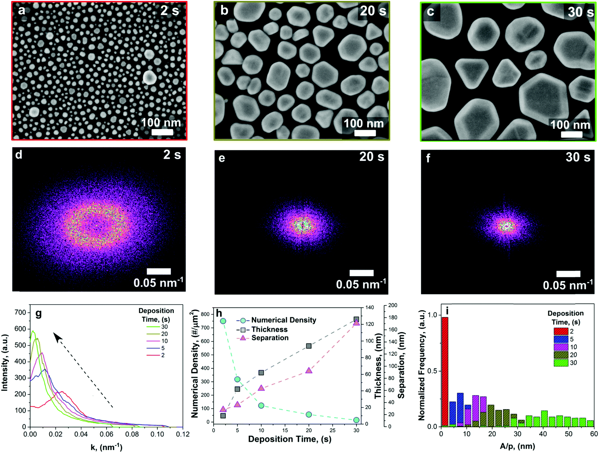 | ||
| Fig. 1 (a–c) Top-view SEM images of the as prepared Au NI films as a function of the deposition time, from 2 to 30 s. (d–f) Two-dimensional FFT of the respective samples showing the organized disorder features indicated by the circular rings in the reciprocal space. (g) Radial profile plot of the circular disks in (d–f) showing a tailorable organized disorder. (h) Computed NI numerical density, average thickness and mean interparticle distance measured from SEM images. (i) Probability histogram for the shape descriptor, defined as the area/perimeter of the NIs normalized with their averaged radius, evaluated for different deposition times. | ||
 | ||
| Fig. 2 (a) Optical reflection measurements and (b) XRD patterns of the correlated disordered Au NI films as a function of the deposition time from 1 s to 30 s. | ||
The synthesized Au NI substrates show a correlated disorder, which can be quantified by defining a structure factor in the inverse space S(k), where k is a frequency vector in the Fourier space, which relates to the degree of homogeneity of the image. In our case, the structure factor S(k) = S(k) because of radial isotropy.
2.3 Electrodynamic simulations
Numerical simulations based on the finite element method (FEM) were carried out using the commercial software CST Microwave Studio in order to investigate the electrodynamic behaviour of different Au NIs on the Si substrate. The simulation geometries were built from the binarization of top-view SEM images of each sample, considering always an area of 500 × 400 nm. Permittivity of Au and Si were obtained from the Johnson and Cristy25 and Palik26 optical constants, respectively. Open boundaries were chosen and terminated with a perfectly matched layer (PML) in order to avoid the wave reflection at the interface. At least 1 × 10⁶ tetrahedral mesh cells were chosen for all the structures, with a particular mesh refinement on the gold sphere in order to increase the precision and convergence of the solver.2.4 SERS measurements
A Renishaw inVia reflex spectrometer system was employed for the SERS measurements. A 633 nm laser was used as the excitation source for the detection of Raman reported rhodamine 6G (R6G) and 5,5′-dithiobis(2-nitrobenzoic acid) (DTNB). The grating was set to 2400 l nm−1 and an objective lens of 20× was used to focus the beam. The integration time was chosen to be 1 s with 3 accumulations (a total of 3 s for the measurement). Under these conditions, the laser power was estimated to be 7 mW and the spot-size has a diameter of 4 μm. R6G and DTNB were purchased from Sigma-Aldrich and dissolved in deionized water with the purpose of obtaining solutions with concentrations ranging from 10−3 to 10−10 M. Before acquiring the measurement, 2 μL of solution was drop-casted on the SERS substrate and allowed to evaporate in an air atmosphere.3. Results and discussion
3.1 Morphological characterization
The synthesis of single crystals of plasmonic Au nanoclusters with a tuneable disorder relies on the Brownian nature of the nanoparticle aerosol deposition process.24 After the precursor solution containing HAuCl4 is atomized, evaporation of the solvent and decomposition of the gold salt in the high-temperature spray flame result in an oversaturated aerosol of Au nanoclusters. The latter nucleate and coalesce in the diffusion-limited regime before reaching the Si substrate's surface.27 In this region, the Au sub-nanometer clusters experience a combination of a steep temperature gradient, namely thermophoretic velocity, diffusion and drag forces. This causes a high frequency of particle collisions within the hot aerosol, which leads to an erratic movement similar to a random-walk, which is usually referred to as Brownian motion. This has important consequences for the direct deposition of plasmonic clusters, resulting in self-similar properties and stochastically distributed hot-spots.The deposition of Au NIs can be controlled by varying the exposure time of the Si wafer to the Au aerosol, resulting in tuneable Au particle sizes, gaps between particles and a high faceting degree with excellent SERS properties. From the top-view SEM images (Fig. 1a–c and the S1, ESI†), it was observed that increasing the exposure time results in larger Au NIs with a decrease in numerical density. The morphological analysis of the lower-magnification SEM images further confirmed the large-scale uniformity of the Au nucleation and growth process (Fig. 1a–c and ESI†). It was observed that increasing the Au aerosol exposure time results in larger NIs with a decrease in numerical density, due to the surface coalescence of the Au nano-islands. Importantly, all the aerosol deposition times result in high uniformity over large scales, providing a means for the facile fabrication of tuneable SERS substrates.
Notably, all the substrates show self-similar tailorable features typical of correlated disordered topologies. This is supported by the analysis in the inverse space (Fig. 1d–f and ESI†). Architectures with organized disorder show a Fourier spectrum consisting of diffusive scattering circularly symmetric rings, which are indications of morphological local structure correlations.28–30 The two-dimensional Fourier power spectral density function of the corresponding substrates (Fig. 1a–c) was obtained by using a 2D fast-Fourier transform (FFT) filtering with Gwyddion v2.52, which provides the structural correlation information in the reciprocal space.31 Interestingly, increasing the deposition time decreases the total dimension of the ring and enhances the intensity. This provides a means to tune the disorder of these plasmonic surfaces (Fig. 1g). This tuneable correlated disorder of the Au NIs favours the presence of organized and well-distributed nano-structures. It also reveals spatially isotropic subwavelength nanostructures with vanishing long-range density fluctuations, which indicates a large degree of homogeneity all across the surface of the sample, despite the stochastic nature of the self-assembly process.21
In addition, the NI density was observed to decrease exponentially with increasing deposition time. For instance, at an exposure time of 2 s, the number of NIs within an area of 3200 × 2400 nm was 5761, and it drastically reduced to 113 NIs for an aerosol deposition time of 30 s. By fitting the numerical density (Nis per μm2) with an exponential function, we found a decay constant of τ = 3.4 s (Fig. 1h, light blue line). This value represents the scaling time for Au NI growth by coalescence during aerosol exposure. As the exposure time increases, the coagulation and coalescence mechanism favour the formation of larger Au particles that grow by incorporating the smaller ones. This, in turn, increases the average interparticle distance from 26 nm to 174 nm (Fig. 1h, purple triangles). As a result, both the particle size and gap between the NIs can be controlled by the aerosol exposure time. Simultaneously, the measured thickness of the Au NI film, evaluated from cross-sectional SEM images (Fig. 1h, grey line), reveals a sharp increase during the first 5 s of deposition followed by a linear growth up to the investigated deposition time of 30 s. In order to quantify the faceting degree, we defined a shape descriptor parameter as the ratio of the averaged area and perimeter of Au NIs, considering the full width at half maximum (FWHM) of the outcome distribution. The broader the distribution, the farther the particles are from a circular shape, hence providing more edges and facets. Fig. 1i shows the probability histogram for different deposition times as a function of the shape parameters. Fitting these data with a normal distribution provides an increasing FWHM, which increases from less than 3 nm up to 27 nm as the deposition time increases from 2 to 30 s. For short deposition times, almost all the Au NIs have a circular shape as indicated by the sharp histogram representation and the SEM images. For 5 and 10 s deposition times, the values of the FWHM are close, reaching 9.3 and 9.6 nm, respectively. This indicates that the faceting process occurs in this timeframe. After this threshold time, the growth of NIs continued due to the oncoming Au adatoms from the aerosol and the coalescence process, with continuously more regular shapes formed, as expressed by the broad (FWHM = 27 nm) histogram distribution.24 This phenomenon, which favours the rise of faceted nanocrystals, leads to a large surface density of hot-spots, where the near-field is drastically enhanced. Furthermore, the latter and the homogeneously distributed structures, arising due to the tuneable organized disorder, are promising features for the realization of optimal SERS substrates.
The control over the particle size and shape is also reflected in the optical properties of the SERS substrates. Fig. 2a shows the reflectance of the disordered Au NI films for the different deposition times. For an aerosol deposition time as short as 1 s, a uniform film with an average Au NI radius of ∼8 nm is formed, showing a small plasmonic resonance band peaked at around 520 nm (Fig. 2a, black line). Upon increasing the deposition time, the LSPR band red-shifts, broadens and increases in strength, as expected from the increasing average particle size. Notably, when the deposition time reaches 10 s, a second peak can be observed in the film reflectance. This is attributed to the increasing amount of regular nanostructures, which also influences the optical properties.32 In particular, the rise of this secondary peak was previously observed in concordance with the emergence of well-defined nano-prism structures.33 Gilroy et al. reported the insurgence of this peak while studying the shape-change of Au spheroidals when exposed to Ag vapour, and they found that the low-wavelength quadrupole peak becomes sharper with an increase of the regularity of the nano-prism structure.34 This is in line with our SEM images and faceting degree, confirming that a shape transformation starts to occur within 10 s of aerosol deposition. Fig. 2b shows the X-ray diffraction (XRD) patterns of the Au NI films with different deposition times. The highly crystalline structures could be confirmed from the characteristic first two Bragg reflections of a face-centered-cubic lattice, corresponding to the [111] and [200] crystallographic planes of Au. Interestingly, the ratio between those planes increases with increasing deposition time, indicating the likelihood of the Au atoms to accommodate in the most energetically stable state, rearranging themselves into highly ordered faceted structures.35,36
3.2 SERS performance
Raman measurements with two standard reporters, namely 5,5′-dithio-bis(2-nitrobenzoic acid) (DTNB) and rhodamine 6G (R6G), were performed in order to evaluate the surface enhancement performance of these substrates. Here, DTNB and R6G were used due to their high SERS cross-section of 10−23–10−24 cm2 sr−1.12,37Fig. 3a shows the SERS spectra obtained from the Au NI substrates with different deposition times under an exposure of 10−4 M DTNB. The most intense peak observed at 1340 cm−1 is assigned to the symmetric stretching of the nitro (–NO2) group.38 A large band at around 1070 cm−1 is due to the succinimidyl N–C–O stretch overlapping with aromatic ring modes, while the aromatic ring stretching mode is responsible for the peak at 1558 cm−1.38 The feature at 1151 cm−1 is assigned to CH3 rocking.39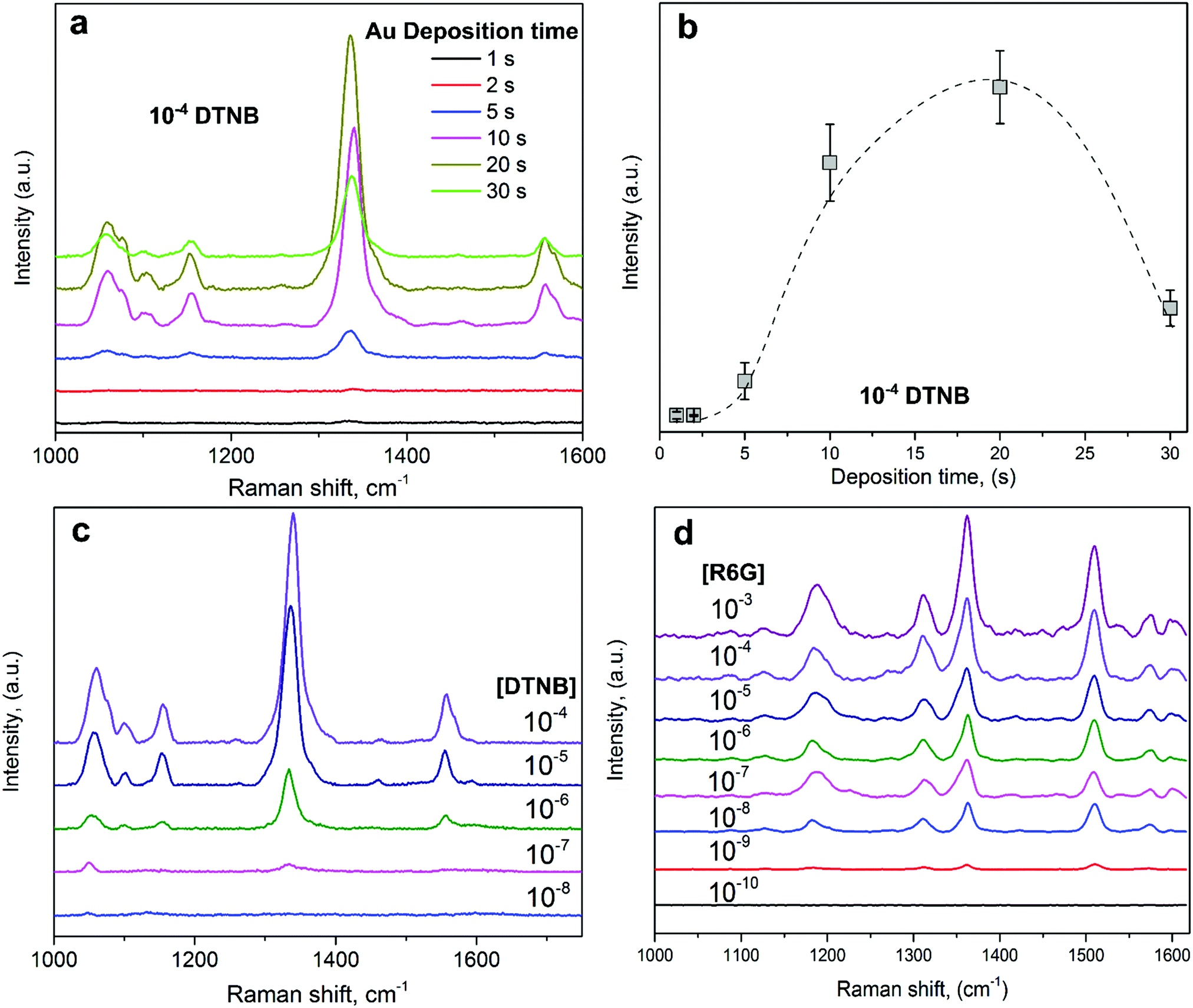 | ||
| Fig. 3 (a) SERS enhancement of 10−4 M DTNB for the various Au NI substrates. (b) SERS intensity as a function of the aerosol-deposition time shows an optimal amplification for the 20 s sample. (c and d) SERS spectra for the detection limit of DTNB and R6G, respectively. | ||
The NI substrates respond differently to the same reporter concentration, showing a maximum SERS intensity for the 20 s deposition time substrate (Fig. 3b). For shorter deposition times (<5 s), the surface enhancement is weak due to the small LSPR response of the sample. As confirmed by the SEM analysis, with a precise tuning of the deposition time, it is possible to drive and control the faceting process of the Au nanostructures. The strong response of the 20 s substrate is attributed to the very good coupling between the laser radiation and the plasmonic wavelength and, in addition, to the controlled faceting degree of these closely packed Au Nis, which increases the generation of hot spots, thus resulting in a strong surface Raman enhancement; this further explains the sharp increase of the SERS intensity observed up to the deposition time of 20 s. For longer deposition times (>20 s), regardless of the increasing faceting degree and disorder level (summarized in Fig. 1g), the SERS enhancement decreases again because of a decrease in the Au NI density. This is due to the increased NI particle size and separation, which lead to a preferentially non-radiative excitation that, in turn, results in a weakened near-field and the diminished SERS intensity.40–43
To further investigate the detection limits of these substrates, the optimal NIs with a deposition time of 20 s were exposed to a continuously decreased concentration of DTNB (Fig. 3c). The characteristic spectral features of DTNB were always resolvable down to a concentration of 10−7 M, while further decreasing the concentration to 10−8 resulted in no detectable SERS enhancement, indicating a detection limit of 10−7 M for this Raman probe.
These optimal SERS substrates were thereafter tested with another Raman reporter, R6G, with concentrations ranging from 10−3 to 10−10 M. Fig. 3d shows the characteristic Raman spectra obtained with these substrates under different concentrations of the R6G reporter. Four dominant peaks can be observed at 1186, 1310, 1362, and 1509 cm−1. The first is attributed to the in-plane bending of the C–H group, while the rest are due to the C–C stretching of the aromatic ring.44 These four peaks are still resolvable down to a concentration of 10−9 M, showing a good detection limit of our optimal NI substrate towards this reporter. In addition, upon exposure to different concentrations of R6G, the reflectance spectra of the bare Au NI substrates show a redshift at the plasmonic resonance. This is coherent with Mie theory and arises from the refractive index change in great proximity to the metallic scatterers, which is transduced into a wavelength shift (S3, ESI†).
An approximate expression was applied to calculate the experimentally measured enhancement factor (EF) of our optimized Au NI SERS substrate with 20 s deposition time:7
 | (1) |
 , where NA is the Avogadro number, h is the penetration depth of the laser (20 μm) and ρ and MW are the density and molecular weight of R6G, respectively. Finally, considering the intensity at 1362 cm−1, the EF was evaluated to be between 107 and 108. While this standard drop-casting procedure followed by natural drying has been utilized in numerous studies,47–51 it requires the assumption of the formation of an analyte monolayer. This assumption is highly controversial and in the past it has led to an erroneous EF.12 In order to validate this assumption and promote the formation of a monolayer, we further drop-cast 10 μL of 10−4 M R6G solution on the Au NI substrates and let them dry naturally. Thereafter, these dropcasted substrates were gently rinsed with ethanol to remove any excess dye and induce the presence of a monolayer. The enhancement factor was then evaluated on these washed substrates to be 1.3 × 10⁷ (S4, ESI†). Notably, this is still sufficient for the detection of single molecules.12,43 Comparing with other recent works based on disordered nano-island structures (see Table 1), our optimized samples hold great potential and advantages towards synthesizing SERS substrates with a comparatively high EF as well as providing a new platform for studying the hyperuniform disorder properties of plasmonic nanostructures.
| Substrate | Synthesis | Excitation wavelength (nm) | Raman probe | EF | Detection limit (M) | Ref. |
|---|---|---|---|---|---|---|
| Au NIs on Si wafer | Flame spray pyrolysis | 633 | Rhodamine 6G (R6G) | 107–108 | 10−9 | This work |
| Silver–gold nano island | Self-assembled out-diffusion technique | 532 | Rhodamine 6G (R6G) | NA | 10−6 | 52 |
| Au on glass or silicon | Solution processing of colloidal nanoparticles and annealing | 633 | 4-Mercaptopyridine | 107 | 10−4 | 53 |
| Au NIs on quartz | Repeated solid-state dewetting | 633 | Benzenethiol (BT) | 2.0 × 10⁷ | 10−7 | 54 |
| Glass nanopillar arrays with nanogap-rich Ag NIs | Reactive ion etching with annealed Ag nanoisland mask and additive Ag deposition | 633 | DNA base molecules | 107 | 10−9 | 55 |
| Magnetron-stabilized Ag NIs on glass | DC and RF magnetron deposition | 633 | Methylene blue (MB) | ∼106–107 | 10−10 | 56 |
| Polymer-Au NIs | Chemical reduction of chloroauric acid | 633 | 4-Aminothiophenol (ATP) | 1.02 × 10⁷ | 10−9 | 57 |
| Au NIs on thiolated glass | Seed-mediated growth process | 633 | Aminothiophenol (ATP) | 3.2 × 10⁸ | 10−8 | 19 |
| Ag NIs on dragonfly wing | Magnetron sputtering deposition | 532 | 4-Aminothiophenol (ATP) | 1.05 × 10⁵ | 10−10 | 58 |
| Ag NIs on ZnO nanosheets | Ultraviolet light-induced photochemical reaction | 633 | Crystal violet (CV) | ∼107 | 10−9 | 59 |
3.3 Electrodynamic simulation
To provide further insights into the performance of these self-assembled NI surfaces and understand the effect of tailorable disorder and high faceting degree on the SERS performance, electrodynamic simulations were conducted for the various Au layouts. Fig. 4a–d show the bi-dimensional map of the electric field distributions at resonance produced for various Au NI substrates, obtained from the SEM images. Due to the reactivity of the free electrons within metallic nanostructures, all Au NI films promptly interact with the incident electromagnetic radiation. Among these, the 2 s deposition time sample (Fig. 4a) shows the lowest near-field enhancement, a feature that may be attributed to the small average dimension and circular shape of the NIs, which led to ineffective SERS performances, and coherently with the reflectance measurements, it showed a small LSPR band. Upon increasing the deposition time to 10 s, a clear conformational change with the appearance of homogeneously distributed faceted Au NIs leads to the formation of several hot spots (Fig. 4b). Consequently, a five-fold increase of the average near-field enhancement can be observed in comparison to the previous sample with 2 s deposition time. Coherent with the SEM analysis, a further increase of the deposition time to 20 s leads to a linear growth of the faceted crystals, resulting in stochastically distributed Au NIs with long-range periodicity and supporting a strong LSPR band at ca. 630 nm. Interestingly, this is reflected in a drastic near-field enhancement (Fig. 4c). Notably, the highly faceted Au NIs and the uniformity of the hot-spots provided by the correlated disorder produce an almost striking coupling with the incident laser radiation (633 nm),60 suggesting that an optimal SERS platform is achieved at 20 s Au deposition. Finally, increasing the deposition time to 30 s decreases the near-field enhancement, despite the higher faceting degree achieved, due to the increased average inter-particle distance (Fig. 4d). This effect dominates over the faceting degree and contributes to a decrease in the plasmonic coupling, which drastically affects the field amplification.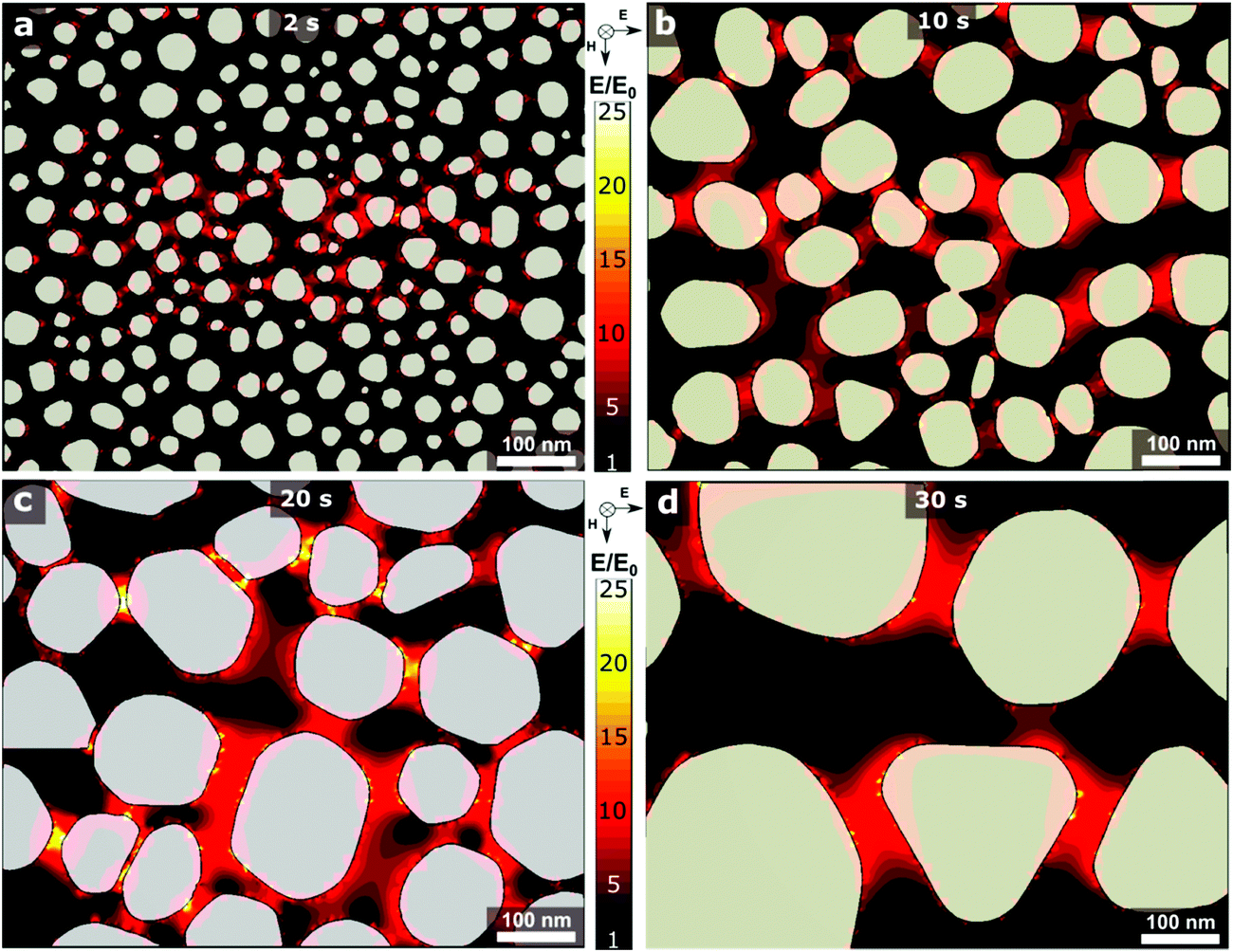 | ||
| Fig. 4 (a–d) FEM simulations of the electric field distribution for various Au NI SERS substrates as a function of the aerosol deposition time. | ||
4. Conclusions
Here, we have presented a facile and scalable route to fabricate well-controlled metallic nano-islands with organized disorder and large-scale uniformity. By controlling the Au nanoparticle aerosol deposition time, a series of Au NI films with tuneable disorder, particle sizes, geometric shapes and nano-scale gaps between the particles was synthesized. It was found that an optimal deposition time of 20 s leads to the optimal compromise between Au faceting and interparticle distance, resulting in the best SERS performance. These optimal NI films resulted in high performance Au SERS substrates reaching an EF as high as 107 and 108 towards R6G, which is sufficiently high for single-molecule detection. The FEM simulations provided further insight into the role of faceting and interparticle distance, showing an initially rapidly increasing and thereafter decreasing hot spot density with the aerosol deposition time. Given the high reproducibility and flexibility of our approach, these findings provide a potential tool for the design and fabrication of metallic nano-structures supporting organized disorder on large-scales with great uniformity for future applications as ultra-sensitive scattering surfaces. Furthermore, novel insights into the correlation between organized disorder and SERS performance are of interest both from a fundamental perspective to investigate the light scattering properties of non-periodic aggregates and for applications ranging from ultra-sensitive spectroscopy to photonic devices designed to support correlated disorder structures.Conflicts of interest
There are no conflicts to declare.Acknowledgements
The authors acknowledge the financial support by the Australian Research Council. A. T. gratefully acknowledges the support of the Australian Research Council DP150101939, the Australian Research Council DE160100569 and the Westpac2016 Research Fellowship and the use of the Australian National Fabrication Facility (ANFF), ACT Node, as well as the Centre of Advanced Microscopy (CAM) at ANU.References
- G. Zito, G. Rusciano, G. Pesce, A. Dochshanov and A. Sasso, Nanoscale, 2015, 7, 8593–8606 RSC
.
- M. Fleischmann, P. J. Hendra and A. J. McQuillan, Chem. Phys. Lett., 1974, 26, 163–166 CrossRef CAS
- E. J. Blackie, E. C. L. Ru and P. G. Etchegoin, J. Am. Chem. Soc., 2009, 131, 14466–14472 CrossRef CAS PubMed
- High Surface-Enhanced Raman Scattering (SERS) sensitivity of R6G by fabrication of silver nanoparticles over GaN nanowires, 11th IEEE International Conference on Nanotechnology, 2011, pp. 297–300, DOI:10.1109/NANO.2011.6144370.
- N. A. Hatab, C.-H. Hsueh, A. L. Gaddis, S. T. Retterer, J.-H. Li, G. Eres, Z. Zhang and B. Gu, Nano Lett., 2010, 10, 4952–4955 CrossRef CAS PubMed
- D. L. Jeanmaire and R. P. Van Duyne, J. Electroanal. Chem. Interfacial Electrochem., 1977, 84, 1–20 CrossRef CAS
- P. L. Stiles, J. A. Dieringer, N. C. Shah and R. P. Van Duyne, Annu. Rev. Anal. Chem., 2008, 1, 601–626 CrossRef CAS PubMed
- H. Ko, S. Singamaneni and V. V. Tsukruk, Small, 2008, 4, 1576–1599 CrossRef CAS PubMed
- Z. Fusco, M. Rahmani, R. Bo, R. Verre, N. Motta, M. Käll, D. Neshev and A. Tricoli, Adv. Mater., 2018, 30, 1800931 CrossRef PubMed
- D. K. Lim, K. S. Jeon, J. H. Hwang, H. Kim, S. Kwon, Y. D. Suh and J. M. Nam, Nat. Nanotechnol., 2011, 6, 452–460 CrossRef CAS PubMed
- W. Yue, Z. Wang, J. Whittaker, F. Lopez-royo, Y. Yang and A. V. Zayats, J. Mater. Chem. C, 2017, 5, 4075–4084 RSC
- E. C. Le Ru, E. Blackie, M. Meyer and P. G. Etchegoin, J. Phys. Chem. C, 2007, 111, 13794–13803 CrossRef CAS
- K. Li, M. I. Stockman and D. J. Bergman, Phys. Rev. Lett., 2003, 91, 227402 CrossRef PubMed
- K. Kneipp, H. Kneipp, I. Itzkan, R. R. Dasari and M. S. Feld, Chem. Rev., 1999, 99, 2957–2976 CrossRef CAS PubMed
- R. Esteban, R. W. Taylor, J. J. Baumberg and J. Aizpurua, Langmuir, 2012, 28, 8881–8890 CrossRef CAS PubMed
- J. Turkevich, P. C. Stevenson and J. Hillier, Discuss. Faraday Soc., 1951, 11, 55–75 RSC
- M. Brust, M. Walker, D. Bethell, D. J. Schiffrin and R. Whyman, J. Chem. Soc., Chem. Commun., 1994, 801–802, 10.1039/C39940000801
- M. Verma, A. Kedia, M. B. Newmai and P. S. Kumar, RSC Adv., 2016, 6, 80342–80353 RSC
- B. N. Khlebtsov, V. A. Khanadeev, E. V. Panfilova, D. N. Bratashov and N. G. Khlebtsov, ACS Appl. Mater. Interfaces, 2015, 7, 6518–6529 CrossRef CAS PubMed
- S. Nie and S. R. Emory, Science, 1997, 275, 1102–1106 CrossRef CAS PubMed
- C. De Rosa, F. Auriemma, C. Diletto, R. Di Girolamo, A. Malafronte, P. Morvillo, G. Zito, G. Rusciano, G. Pesce and A. Sasso, Phys. Chem. Chem. Phys., 2015, 17, 8061–8069 RSC
- R. Aroca and F. Martin, J. Raman
Spectrosc., 1985, 16, 156–162 CrossRef CAS
- P. Pavaskar, I.-K. Hsu, J. Theiss, W. H. Hung and S. B. Cronin, J. Appl. Phys., 2013, 113, 034302 CrossRef
- Z. Fusco, M. Rahmani, R. Bo, T. Tran-Phu, M. Lockrey, N. Motta, D. Neshev and A. Tricoli, Adv. Funct. Mater., 2019, 29, 1806387 CrossRef
- P. B. Johnson and R. W. Christy, Phys. Rev. B: Condens. Matter Mater. Phys., 1972, 6, 4370–4379 CrossRef CAS
-
Handbook of Optical Constants of Solids, ed. E. D. Palik, Academic Press, Burlington, 1997, p. 1000 Search PubMed
- B. Buesser and S. E. Pratsinis, Annu. Rev. Chem. Biomol. Eng., 2012, 3, 103–127 CrossRef CAS PubMed
- M. Castro-Lopez, M. Gaio, S. Sellers, G. Gkantzounis, M. Florescu and R. Sapienza, APL Photonics, 2017, 2, 061302 CrossRef
- A. Jouanin, J. P. Hugonin and P. Lalanne, Adv. Funct. Mater., 2016, 26, 6215–6223 CrossRef CAS
- E. R. Martins, J. Li, Y. Liu, V. Depauw, Z. Chen, J. Zhou and T. F. Krauss, Nat. Commun., 2013, 4, 2665 CrossRef PubMed
- S. Yu, C. Wang, Y. Zhang, B. Dong, Z. Jiang, X. Chen, W. Chen and C. Sun, Sci. Rep., 2017, 7, 3752 CrossRef PubMed
- V. C. Verma, S. K. Singh, R. Solanki and S. Prakash, Nanoscale Res. Lett., 2011, 6, 16 CrossRef PubMed
- M. Verma, A. Kedia, M. B. Newmai and P. S. Kumar, RSC Adv., 2016, 6, 80342–80353 RSC
- K. D. Gilroy, A. Sundar, M. Hajfathalian, A. Yaghoubzade, T. Tan, D. Sil, E. Borguet, R. A. Hughes and S. Neretina, Nanoscale, 2015, 7, 6827–6835 RSC
- X. Sun, S. Dong and E. Wang, Angew. Chem., Int. Ed., 2004, 43, 6360–6363 CrossRef CAS PubMed
- B. Ankamwar, M. Chaudhary and M. Sastry, Synth. React. Inorg., Met.-Org., Nano-Met. Chem., 2005, 35, 19–26 CrossRef CAS
- J. A. Dieringer, K. L. Wustholz, D. J. Masiello, J. P. Camden, S. L. Kleinman, G. C. Schatz and R. P. Van Duyne, J. Am. Chem. Soc., 2009, 131, 849–854 CrossRef CAS PubMed
- D. S. Grubisha, R. J. Lipert, H.-Y. Park, J. Driskell and M. D. Porter, Anal. Chem., 2003, 75, 5936–5943 CrossRef CAS PubMed
- A. Kamińska, K. Winkler, A. Kowalska, E. Witkowska, T. Szymborski, A. Janeczek and J. Waluk, Sci. Rep., 2017, 7, 10656 CrossRef PubMed
- M. Moskovits, J. Raman Spectrosc., 2005, 36, 485–496 CrossRef CAS
- N. D. Israelsen, C. Hanson and E. Vargis, Sci. World J., 2015, 2015, 12 Search PubMed
- S. Hong and X. Li, J. Nanomater., 2013, 2013, 9 Search PubMed
- E. C. Le Ru and P. G. Etchegoin, MRS Bull., 2013, 38, 631–640 CrossRef
- T. T. B. Quyen, C.-C. Chang, W.-N. Su, Y.-H. Uen, C.-J. Pan, J.-Y. Liu, J. Rick, K.-Y. Lin and B.-J. Hwang, J. Mater. Chem. B, 2014, 2, 629–636 RSC
- H. Jia, X. Bai, N. Li, L. Yu and L. Zheng, CrystEngComm, 2011, 13, 6179–6184 RSC
- R. Sasai, T. Fujita, N. Iyi, H. Itoh and K. Takagi, Langmuir, 2002, 18, 6578–6583 CrossRef CAS
- H. Dies, J. Raveendran, C. Escobedo and A. Docoslis, Nanoscale, 2017, 9, 7847–7857 RSC
- G. B. Jung, Y. M. Bae, Y. J. Lee, S. H. Ryu and H.-K. Park, Appl. Surf. Sci., 2013, 282, 161–164 CrossRef CAS
- R. Botta, G. Upender, R. Sathyavathi, D. Narayana Rao and C. Bansal, Mater. Chem. Phys., 2013, 137, 699–703 CrossRef CAS
- Z. Xu, M. R. Gartia, C. J. Choi, J. Jiang, Y. Chen, B. T. Cunningham and G. L. Liu, J. Raman Spectrosc., 2011, 42, 1939–1944 CrossRef CAS
- Y. Liu, S. Xu, H. Li, X. Jian and W. Xu, Chem. Commun., 2011, 47, 3784–3786 RSC
- E. Babich, A. Redkov, I. Reduto and A. Lipovskii, Phys. Status Solidi, 2018, 12, 1700226 Search PubMed
- H. Liu, X. Zhang, T. Zhai, T. Sander, L. Chen and P. J. Klar, Nanoscale, 2014, 6, 5099–5105 RSC
- M. Kang, S.-G. Park and K.-H. Jeong, Sci. Rep., 2015, 5, 14790 CrossRef CAS PubMed
- Y.-J. Oh and K.-H. Jeong, Adv. Mater., 2012, 24, 2234–2237 CrossRef CAS PubMed
- M. Subr, M. Petr, O. Kylian, J. Kratochvil and M. Prochazka, J. Mater. Chem. C, 2015, 3, 11478–11485 RSC
- X. Zhou, F. Zhou, H. Liu, L. Yang and J. Liu, Analyst, 2013, 138, 5832–5838 RSC
- Y. Wang, M. Wang, L. Shen, X. Sun, G. Shi, W. Ma and X. Yan, Appl. Surf. Sci., 2018, 436, 391–397 CrossRef CAS
- L. Xu, S. Li, F. Li, H. Zhang, D. Wang, M. Chen and F. Chen, Opt. Mater. Express, 2017, 7, 3137–3146 CrossRef CAS
- R. A. Alvarez-Puebla, J. Phys. Chem. Lett., 2012, 3, 857–866 CrossRef CAS PubMed
Footnotes |
| † Electronic supplementary information (ESI) available. See DOI: 10.1039/c9tc01231a |
| ‡ These authors have equally contributed to the manuscript. |
| This journal is © The Royal Society of Chemistry 2019 |