
High-resolution organic field-effect transistors manufactured by electrohydrodynamic inkjet printing of doped electrodes†
Jing
Zhang
a,
Bowen
Geng
ab,
Shuming
Duan
a,
Congcong
Huang
a,
Yue
Xi
a,
Qi
Mu
b,
Huipeng
Chen
c,
Xiaochen
Ren
*a and
Wenping
Hu
 *a
*a
aTianjin Key Laboratory of Molecular Optoelectronic Sciences, Department of Chemistry, School of Science, Tianjin University & Collaborative Innovation Center of Chemical Science and Engineering (Tianjin), Tianjin, 300072, China. E-mail: renxiaochen@tju.edu.cn; huwp@tju.edu.cn
bSchool of Microelectronics, Tianjin University, Tianjin, 300072, China
cInstitute of Optoelectronic Display, National & Local United Engineering Lab of Flat Panel Display Technology, Fuzhou University, Fuzhou 350002, China
First published on 16th July 2020
Abstract
Electrohydrodynamic inkjet (E-jet) printing is a promising technology to fabricate high-performance organic electronic devices due to its high resolution, low-cost and drop-on-demand characteristics. Here, we fabricate top-contact OFETs by using E-jet printed source/drain electrodes. The printed resolution could be smaller than 5 μm on an organic semiconductor. A printable Ag ink consisting of the F4-TCNQ additive greatly improves the charge injection of the OFET, and thus the OFETs show comparable performance with thermally evaporated electrodes. The printing and doping of top electrodes can be realized in one step, which is essential to realize fully printed organic devices. The E-jet printing demonstrates its potential in high-resolution, high-performance OFET applications.
Electronic devices based on organic semiconductors have several unique advantages such as intrinsic flexibility, tunable electrical properties and solution processability.1,2 Solution processability allows the fabrication of organic electronic devices by using various printing methods such as ink-jet printing, screen printing, gravure printing and so on,3 avoiding the use of vacuum or photolithography processing, and thus significantly reducing the fabrication cost. Organic field-effect transistors (OFETs) are the fundamental unit of organic integrated circuits. The fabrication of the source/drain electrodes of OFETs by printing is usually realized by bottom contact configuration4 because the solvent in the ink may damage the organic active layer if a top contact device structure is applied. However, bottom contact OFETs always suffer from severe contact resistance issues that hinder the device performance.5–7
Meanwhile, most of metal based conductive inks are made of Ag nanoparticles or nanoflakes.8 The work function of Ag in the nanoparticle form is around 4.4 eV.9 A mismatch between the work function of electrodes and the highest occupied molecular orbital (HOMO) of organic semiconductors occurs for commonly used high-performance p-type organic semiconductors such as dinaphtho[2,3-b:2′,3′-f]thieno[3,2-b]thiophene (DNTT), 2,7-dioctyl[1]benzothieno[3,2-b][1]benzothiophene (C8-BTBT) or 2,6-diphenyl anthracene (DPA),10–12 resulting in a potentially large charge injection barrier. Appropriate doping of the organic semiconductor is highly preferred to improve the charge injection, which can be processed either by depositing the dopant on the surface of the host semiconductor or electrode, or by adding the dopant into the host semiconductor or electrodes through a co-evaporation or solution processing technique such as molecular implantation.13–15 Among those methods, the development of the solution processed doping method is urgent since it is fully compatible with the current printing techniques, without the need for introducing an extra vacuum process. Resolution is another important concern for printed electrodes, because the channel length of OFETs as well as the overlap area between the drain/source electrodes and gate electrode determines the operating frequency of the OFETs.16 A MHz working range organic transistor device typically requires the channel length to be smaller than 10 μm,17 which is beyond the resolution of common printing techniques including ink-jet printing, screen printing or gravure printing.18 Electrohydrodynamic inkjet (E-jet) printing is a promising printing method because its droplet volume could approach the femtoliter (fL) range,19 significantly enhancing the printing resolution and reducing the solvent damaging effect, although its application in OFETs has been rarely reported.20
In this work, we fabricated top-contact OFETs by using E-jet printed source/drain electrodes. The fL volume droplet of E-jet printing allows direct printing onto the organic semiconductor without solvent damage, and the sintering temperature of the printed electrodes could be down to 80 °C because of the trace amount of solvent. The printed line width/spacing could be smaller than 5 μm on an organic semiconductor. A printable Ag ink containing F4-TCNQ additive greatly improves the charge injection of the OFET, and thus the OFETs based on E-jet printed top electrodes with channel length less than 15 μm show comparable performance with thermally evaporated electrodes. The printing and doping of top electrodes can be realized in one step, which is essential to realize fully printed organic devices. E-jet printing demonstrates its potential in high-resolution, high-performance OFET applications.
The bottom-gate top-contact (BGTC) OFETs were fabricated on heavily doped silicon wafers with 300 nm thermally grown SiO2. Firstly, silicon wafers were cleaned in deionized water (DI), acetone and isopropanol with ultrasonication and then in O2 plasma for 5 min before use. Next, the silicon wafers were soaked in modified solutions and heated at 90 °C for 120 min, forming the octadecyl-trichlorosilane (OTS, J&K Scientific) self-assembled monolayer (SAM), and then the substrate was cleaned with isopropanol and N-hexane separately before deposition. A 40 nm DNTT (Sigma-Aldrich) thin-film was thermally evaporated onto the substrate, while the chamber pressure was maintained at 1 × 10⁻⁶ mbar; the substrate temperature was maintained at 60 ± 3 °C and the deposition rate was controlled at 0.1 ± 0.02 Å s−1. Following this, Ag inks (NPS-J, Harima Chemical Group, Inc.) with/without doping were ejected directly onto the surface of the organic semiconductor thin-film with 5, 15 or 50 μm channel lengths and 300, 500 or 4500 μm channel widths, respectively, by using an SIJ S050 inkjet printer. Finally, the BGTC devices were baked at 80 °C for 120 min in a vacuum oven with a vacuum level of around 0.1 mbar. Electrical characterization was carried out by using a Keithley 4200 SCS in air. A unit-area capacitance of 11.5 nF cm−2 for the SiO2 dielectric is used for mobility calculation. Atomic force microscope (AFM) measurements were done on a Bruker Icon Atomic force microscope, using the tapping mode. Scanning electron microscopy (SEM) measurements were carried out on a Hitachi SU8010, under 10 kV voltage.
The schematic drawing of the setup of the E-jet printer is shown in Fig. 1a. With the help of an electrical field applied between the inkjet nozzle and the substrate, the volume of the fluid jetting from the tail of the droplet could be as small as a femtoliter. The printing resolution is therefore significantly enhanced. By using numerically controlled moving stages, complex shapes can be printed onto the SiO2 substrate by using Ag ink, including a repeated line array, letters and emoticons, as shown in Fig. 1b, in which the average line width is around 5–10 μm. Other than using the default Ag ink, we also added 2,3,5,6-tetrafluoro-7,7,8,8-tetracyanoquinodimethane (F4-TCNQ) as the dopant into the ink in order to improve the charge injection for printed OFETs. The fabrication process of mixed inks is illustrated in Fig. 1c. At first, the F4-TCNQ was fully dissolved in n-tetradecane stirred at 350 rpm for 10 min to make a F4-TCNQ solution with a concentration of 1 mg mL−1, and then F4-TCNQ solution was added into the Ag inks (NPS-J) followed by vigorous stirring to completely mix with the ink. The F4-TCNQ concentration in the final mixed solution ranges from 0.01 to 0.024 mg mL−1.
 | ||
| Fig. 1 (a) Schematic diagram of super inkjet printing. The inset shows a monitoring picture indicating the nozzle distance in the printing process. (b) Photographs of printed complex geometry shape. Scale bars in the pictures are 50 μm. (c) Flow diagram of the process of mixing F4-TCNQ with Ag NPs inks. | ||
Before directly printing the Ag electrodes onto the organic semiconductor, we characterize the conductivity of the printed electrodes to determine the optimum processing parameters. The conductivity of printed lines can be enhanced by using multiple pass printing, but the ink consumption is also increased, which would affect the underlying organic semiconductor. As shown in Fig. 2a, the optical microscope images of printed Ag lines by using doped ink with different printing passes exhibit an obvious morphology difference. The first row of the picture was taken immediately after printing, while the second row of the picture was taken after annealing at 80 °C. The printed material for one-pass printing is evenly distributed inside the line before or after annealing, but the colour fades after annealing. For multiple printing passes, the line width is identical but a coffee-ring like effect is observed, which suggests that the ink is concentrated at the edge of the printed lines before annealing. On the contrary, most of the material moves from the edge to the centre after annealing. The printed material distribution across the lines is further confirmed by AFM height measurements as shown in Fig. 2b; the height at the centre of the printed line is obviously larger than the edge, proving the material redistribution after annealing. The SEM image shown in Fig. 2c suggests that the four times printing pass leads to a continuous distribution of the Ag nanoparticles after annealing, thus guaranteeing the good conductivity of printed lines. By taking the height information from AFM results, the height of the printed lines as a function of the number of printing passes is plotted in Fig. 2d. The thickness of the Ag lines is proportional to the number of printing passes. The effective thickness of the line increases from 15 nm after a single pass to 376 nm after 14 passes. Next, we characterized the electrical conductivity of printed Ag lines with different printing passes. Before measuring, the Ag line is calcinated at a temperature of 80 °C for 1 h in a vacuum and then the resistance is measured at room temperature in air. We used a two-probe method to measure the resistance of the Ag lines with length equal to 1 mm. Fig. 2d shows the resistance of inkjet-printed Ag lines from 4 to 18 printing passes, whereas the resistance of one pass printing is over MΩ, generally not suitable for practical use. The results shown in Fig. 2d suggest that 6 passes are sufficient to obtain a stable resistance of around 60 Ω, which is good enough for OFET applications.
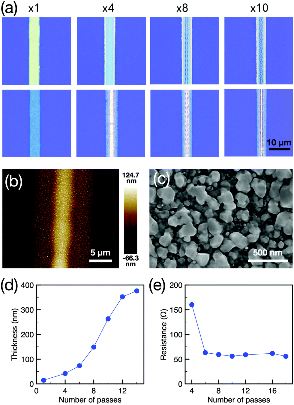 | ||
| Fig. 2 (a) Optical images showing the effect of multiple-pass printing on the evolution of the morphology of an inkjet-printed Ag line before (top) and after (bottom) calcination. (b) AFM (4 printing passes) and SEM (4 printing passes) image of inkjet-printed Ag lines after calcination at 80 °C. (c) The effective thickness of the line increases from 15 nm after a single pass to 376 nm after 14 passes. (d) Resistance of inkjet-printed Ag lines from 4 to 18 printing passes. | ||
The complete OFET device is fabricated using the SiO2 substrate with the OTS self-assembly monolayer as shown in Fig. 3a. The organic small molecular semiconductor DNTT is thermally evaporated as the active layer for its poor solubility and good carrier mobility. The top contact source–drain electrodes are directly printed on DNTT by using Ag NP ink with and without the F4-TCNQ mixture. As shown in Fig. 3b, the channel length of OFET is 15 μm, and the channel width is 450 μm. Fig. 3c plots the transfer I–V curve of OFETs as a function of the F4-TCNQ doping concentration. It is obvious that OFET with pure Ag ink electrodes gives a small saturation drain–source current of around a few μA, and a poor on/off current ratio less than 104. Both the saturation current and on/off ratio improves with increasing concentration of F4-TCNQ from 0.01 or 0.019 mg mL−1; a further increase in F4-TCNQ concentration to 0.024 mg mL−1 leads to slightly reduced channel current and increased off-state current. The saturation field-effect mobility and threshold voltage (Vth) can be obtained by plotting the |ID|(1/2)–VG curves and fitting lines of the linear region of the curves; the slope and the interception of the fitting lines represent the mobility and Vth of the OFETs, respectively. The results are shown in Fig. 3d and e. In addition, to better estimate the mobility value, the reliability factor of saturation mobility rsat is determined21 and is shown in Fig. 3d. All the devices show rsat ranging from 55–70%. The gate bias dependent mobility is also calculated as plotted in Fig. S1 in the ESI.† The mobility of OFETs increase monotonically with F4-TCNQ doping concentration and become saturated at 0.016–0.019 mg mL−1 and then decrease at a concentration of 0.024 mg mL−1. The Vth is generally shifted positively with increasing F4-TCNQ doping concentration from 0.00 to 0.024 mg mL−1. The improved device performance is probably due to the doping effect of F4-TCNQ that lowers the charge injection barrier from drain–source electrodes, and thus the optimum F4-TCNQ doping concentration is 0.016–0.019 mg mL−1. In this condition, the highest mobility of 1.75 cm2 V−1 s−1 is achieved with an on/off ratio larger than 108. This value is comparable to the device using thermally evaporated Au electrodes with larger channel length.11 The result suggests that the performance of direct inkjet printing is as good as that of conventional thermally evaporated electrodes.
 | ||
| Fig. 3 (a) A schematic cross-section of the organic thin film transistors with a vacuum-deposited organic semiconductor and super inkjet-printed Ag nanoparticle source/drain contacts. (b) The optical image of the printing OFETs. (c) Transfer curves of the DNTT thin-film OFETs with different doping concentrations ranging from 0.00 to 0.024 mg mL−1. The dashed lines are the fitting lines on the sweep of the |ID|1/2–VG curves. (d) Plots of the mobility of the FETs and the reliability factor of saturation mobility versus the doping concentration of the ink. (e) The off-to-on (Vth) threshold voltages at different doping concentrations of the silver ink. | ||
To find out the reason why the dopant affects the device performance, we performed the Kelvin probe force microscope (KPFM) measurements of the printed Ag electrodes at various F4-TCNQ concentrations. The Ag electrodes are printed on a bare silicon substrate and then scanned for surface potential measurements. The work function of electrodes is obtained by applying eqn (1) and (2):
| Vsample = VTip + VCPD | (1) |
| Wsample = eVsample | (2) |
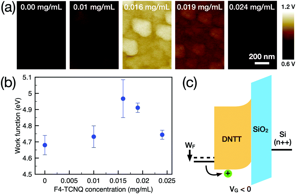 | ||
| Fig. 4 (a) The AFM potential map at different F4-TCNQ concentrations ranging from 0.00 to 0.024 mg mL−1. (b) Plots of the work function of average value versus the doping concentration of the ink. (c) Schematic drawing of the energy band diagram of the OFET at the saturation state. | ||
To demonstrate the repeatability of the printed electrodes, a total of 74 devices were fabricated and measured in air. The statistics of mobility and on/off ratio are shown in Fig. 5a and b, respectively. The devices exhibit an average mobility of 1.55 cm2 V−1 s−1 (μmax = 3.26 cm2 V−1 s−1, μmin = 0.83 cm2 V−1 s−1, and standard deviation of 0.61 cm2 V−1 s−1) in the saturation regime and an average on/off ratio of 2.23 × 10⁷. This result indicates that the E-jet printed electrode maintains an accurate geometrical dimension and highly repeatable electrical characteristics over multiple printing times. A large W/L ratio of OFETs minimizes the uncertainty of charge transport in an organic semiconductor presented by grain boundaries, contributing to the uniform electrical characteristics. The good uniformity of printed electrodes is further demonstrated by printing a 5 × 5 transistor array in a one-time run. The optical images, transfer I–Vs and statistics of the device performance are shown in Fig. S2 (ESI†). All the 25 devices are highly uniform. The maximum mobility of the printed transistor is 1.22 cm2 V−1 s−1, and the average mobility of the 5 × 5 array is 1.01 cm2 V−1 s−1 in the saturation regime. 21 out of 25 devices have an on/off ratio larger than 107. The content of Ag NPs and F4-TCNQ mixed ink shows negligible change during the printing. The stable printing performance enables the application of large-scale printing of OFETs such as display driving backpanel or integrated circuits. The repeatable high-resolution printing of electrodes allows further scaling down of the device dimensions. As a result, the channel length of OFET of around 4 μm is demonstrated in the inset of Fig. 5c; an OFET with W/L ratio >300 is realized by E-jet printing. The current output of such OFETs is ∼8 mA as shown by the transfer I–V in Fig. 5d. OFETs with very large W/L ratio enables the sensing applications with low detectivity, and high current driving circuits for micro-LED arrays or OLED lighting. The mobility of OFET at 4 μm channel length is 1.24 cm2 V−1 s−1, which is slightly lower than the average value. The greater portion of contact resistance in the overall channel resistance at shorter channel length may account for the mobility reduction of the device.
 | ||
| Fig. 5 (a) A histogram of the saturation mobility of 74 OFETs. (b) A histogram of the on/off current ratio of 74 OFETs. (c) The optical image of the printing short channel OFETs. (d) Transfer characteristics of printed OFET with W/L >300. | ||
Conclusion
To summarize, we have realized direct E-jet printed top contact OFETs with channel length down to 5 μm. Multiple pass printing is used to balance the thickness and conductivity of printed electrodes. With appropriate F4-TCNQ doping of the electrodes using the solution method, OFETs with printed electrodes showed comparable performance to those devices with thermally evaporated top electrodes. F4-TCNQ doping increases the work function of electrodes and improves the charge injection of OFETs. The printing process is highly repeatable with small device-to-device variation. An OFET with a channel length of 4 μm and W/L ratio >300 is demonstrated for mA range channel current, enabling high current output application for OFETs. The high-resolution E-jet printing of OFET top contacts is the key step toward high-performance printed organic electronic device fabrication.Conflicts of interest
There are no conflicts to declare.Acknowledgements
The authors acknowledge financial support from the National Key R&D Programs (2017YFA0204503, 2016YFB0401100) and the National Natural Science Foundation of China (91833306, 51633006, 51703159, 51703160, 51733004).Notes and references
- Y. Wu, Y. Li, B. S. Ong, P. Liu, S. Gardner and B. Chiang, Adv. Mater., 2005, 17, 184–187 CrossRef CAS
.
- Y. Xu, C. Liu, D. Khim and Y. Y. Noh, Phys. Chem. Chem. Phys., 2015, 17, 26553–26574 RSC
- B. Kang, W. H. Lee and K. Cho, ACS Appl. Mater. Interfaces, 2013, 5, 2302–2315 CrossRef CAS PubMed
- Y. Noguchi, T. Sekitani, T. Yokota and T. Someya, Appl. Phys. Lett., 2008, 93, 043303 CrossRef
- D. Gupta, M. Katiyar and D. Gupta, Org. Electron., 2009, 10, 775–784 CrossRef CAS
- J. A. Lim, W. H. Lee, H. S. Lee, J. H. Lee, Y. D. Park and K. Cho, Adv. Funct. Mater., 2008, 18, 229–234 CrossRef CAS
- C. Liu, Y. Xu and Y. Y. Noh, Mater. Today, 2015, 18, 79–96 CrossRef CAS
- D. Ye, Y. Ding, Y. Duan, J. Su, Z. Yin and Y. A. Huang, Small, 2018, 14, 1703521 CrossRef PubMed
- S. Gamerith, A. Klug, H. Scheiber, U. Scherf, E. Moderegger and E. J. W. List, Adv. Funct. Mater., 2007, 17, 3111–3118 CrossRef CAS
- Y. Xu, H. Sun, A. Liu, H. H. Zhu, W. Li, Y. F. Lin and Y. Y. Noh, Adv. Mater., 2018, 30, 1801830 CrossRef PubMed
- U. Kraft, K. Takimiya, M. J. Kang, R. Rödel, F. Letzkus, J. N. Burghartz, E. Weber and H. Klauk, Org. Electron., 2016, 35, 33–40 CrossRef CAS
- X. Gao, S. Duan, J. Li, D. Khan, Y. Zou, L. Zheng, J. Liu, X. Ren and W. Hu, J. Mater. Chem. C, 2018, 6, 12498–12502 RSC
- S. D. Wang, Y. Yan and K. Tsukagoshi, Appl. Phys. Lett., 2010, 97, 063307 CrossRef
- B. Lussem, C. M. Keum, D. Kasemann, B. Naab, Z. Bao and K. Leo, Chem. Rev., 2016, 116, 13714–13751 CrossRef CAS PubMed
- R. Fujimoto, Y. Yamashita, S. Kumagai, J. Tsurumi, A. Hinderhofer, K. Broch, F. Schreiber, S. Watanabe and J. Takeya, J. Mater. Chem. C, 2017, 5, 12023–12030 RSC
- F. Ante, D. Kalblein, T. Zaki, U. Zschieschang, K. Takimiya, M. Ikeda, T. Sekitani, T. Someya, J. N. Burghartz, K. Kern and H. Klauk, Small, 2012, 8, 73–79 CrossRef CAS PubMed
- R. Kitsomboonloha, H. Kang, G. Grau, W. Scheideler and V. Subramanian, Adv. Electron. Mater., 2015, 1, 1500155 CrossRef
- L. Shao, T. Y. Chu, Y. Tao and K. T. Cheng, 2018 International Flexible Electronics Technology Conference (IFETC), 2018.
- M. S. Dresselhaus, A. Jorio, M. Hofmann, G. Dresselhaus and R. Saito, Nano Lett., 2010, 10, 751–758 CrossRef CAS PubMed
- T. Sekitani, Y. Noguchi, U. Zschieschang, H. Klauk and T. Someya, Proc. Natl. Acad. Sci. U. S. A., 2008, 105, 4976–4980 CrossRef CAS PubMed
- H. H. Choi, K. Cho, C. D. Frisbie, H. Sirringhaus and V. Podzorov, Nat. Mater., 2018, 17, 2–7 CrossRef CAS PubMed
- O. Rana, R. Srivastava, G. Chauhan, M. Zulfequar, M. Husain, P. C. Srivastava and M. N. Kamalasanan, Phys. Status Solidi A, 2012, 209, 2539–2545 CrossRef CAS
Footnote |
| † Electronic supplementary information (ESI) available. See DOI: 10.1039/d0tc02508a |
| This journal is © The Royal Society of Chemistry 2020 |