DOI:
10.1039/D0TC03244A
(Communication)
J. Mater. Chem. C, 2020,
8, 15099-15104
Permalloy/polydimethylsiloxane nanocomposite inks for multimaterial direct ink writing of gigahertz electromagnetic structures†
Received
9th July 2020
, Accepted 11th September 2020
First published on 14th September 2020
Abstract
In light of society's increasing demand for ubiquitous connectivity and high-speed communication, printed electronics could play a disruptive role in the design and manufacturing of high frequency radiofrequency (RF) passives. However, traditional ink-based printing technologies face significant challenges in their planar device geometries, limited material choices, and poor resolution (∼100 μm), which constrain the design of printable RF passives typically operatable in the kilohertz (kHz) to megahertz (MHz) frequency range. The low resolution of printing technologies also makes it challenging to integrate printed passives with lithography-manufactured active electronics to form RF circuitries with diverse wireless functionalities. Direct ink writing (DIW), on the other hand, allows the high-resolution manufacturing of three-dimensional (3D) device architectures that are critical for applications beyond the frequency of one gigahertz (GHz). However, current DIW-printed RF passives only employ a single conductive ink, which limits the passive device's performance. For example, in solenoidal inductors, the inclusion of a magnetic core would greatly enhance the per-area inductance. Here, we designed and synthesized a permalloy/PDMS magnetic nanocomposite ink by dispersing surface modified permalloy nanoparticles into a PDMS matrix. The optimal weight ratio of permalloy in PDMS was determined based on Bruggeman effective medium theory to afford a high operational frequency while maintaining high-resolution printability. By harnessing the multimaterial DIW of both a conductive silver nanoparticle ink and our new permalloy magnetic ink, we demonstrate printed solenoidal inductors and LC tanks integrating magnetic cores with enhanced inductance.
Introduction
Since the 1980s, printed electronics has quickly evolved from printed circuit boards to many everyday use electromagnetic devices such as radio frequency identification (RFID) devices and antennas.1–4 In light of society's increasing demand for ubiquitous connectivity and high-speed communication, printed electronics could play an even more important role in the manufacturing of high frequency RF passives. Although different ink-based printing technologies such as inkjet printing,5–8 screen printing,9–11 and roll-to-roll printing12 are commonly used in the manufacturing of planar electromagnetic passives, the printed two-dimensional (2D) device architectures, low resolution (∼100 μm), and limited material choices significantly constrain the performance of these devices, which mainly operate in the kilohertz (kHz) to megahertz (MHz) frequency range. Besides, the resolution mismatch between printed components and lithography-based electronics also poses significant challenges in integration with wafer technology to integrate active electronics. Different from those macro-scale printing technologies, the direct ink writing (DIW) approach enables the selective and precise assembly of functional materials in 3D space at the μm-scale, which is readily comparable to the typical feature sizes of RF passives. Briefly, the DIW process employs a high-precision computer-controlled translation stage, on which an ink-deposition nozzle extrudes functional inks continuously to form high aspect ratio, self-supported, free-form 3D architectures.13 In recent years, different complex three-dimensional structures, e.g. microbatteries,14,15 photonic crystals,16 sensors17,18 tissue engineering scaffolds,19etc., were fabricated via the DIW approach due to its rich material choices and high precision. With minimal substrate limitations, DIW provides opportunities for fabricating flexible electronics directly on plastic substrates or 3D electronics by printing conformally non-planar surface topologies.20 Thanks to its high resolution, DIW potentially offers convenient integration with silicon-based active electronics to form complex RF circuitries.21 As the material properties and structures determine the functions, DIW greatly expands the device design freedom and should lead to realization of electromagnetic structures with enhanced functionalities.
In our previous work, we have demonstrated air-core solenoidal inductors printed using viscoelastic silver-nanoparticle inks, with inductance values in the nH range and operating in the frequency range of several gigahertz (GHz).21 Yet the absence of a magnetic core limits the overall inductance per area. Recently, inductors with polymer–magnetic composite cores were printed using aerosol-jet 3D printing of a conductive ink and a UV-curable polymer composite.22 However, the printing resolution is limited (∼100 μm) and the cross-sectional area of the magnetic cores was ∼2 mm2, and the printed devices could only operate in the several kHz to MHz frequency range. In principle, the magnetic core serves to enhance and confine the magnetic flux, improving the areal-L-density, which is crucial for on-chip device integration.23 Soft magnetic materials are widely selected as the magnetic core of inductive coils for increasing inductance, because they exhibit easy magnetization/demagnetization properties when an external magnetic field is switched on/off.24 Previous research on printing soft magnetic materials mainly employed ferrite inks and demonstrated electromagnetic devices operable in the kHz–MHz range.25–27 In comparison with ferrites, permalloy exhibits higher permeability, lower coercivity, and better thermal and oxygen stability,28,29 and it has been used in numerous commercial electromagnetic passives for decades.24 For printed devices employing permalloy inks, current research has only focused on 2D layer-by-layer deposition of permalloy combined with dielectric materials.30–34 Yan et al.35 developed a printable permalloy/thermoset polymer composite ink and created 3D structures using a fused deposition modelling (FDM) 3D printer. The magnetic core is limited to 2 mm printing resolution and stable permeability was observed up to only ∼30 MHz. Therefore, new soft magnetic inks with low loss at high frequency, high-resolution printability, and good stability must be developed to meet the requirement of electromagnetic passives operatable beyond GHz frequencies.
Here, we designed and synthesized a permalloy magnetic nanocomposite ink by dispersing the surface modified permalloy nanoparticles with an average size of 70 nm into a polydimethylsiloxane (PDMS) matrix and used multimaterial printing to pattern GHz electromagnetic architectures integrating both conductive and magnetic features. The non-magnetic PDMS matrix material was incorporated to extend the operational frequencies and provide enhanced thermal stability to the nanocomposite ink.36,37 The optimal weight ratio of permalloy in PDMS was systematically investigated to afford both high operational frequencies and suitable printability.
Results and discussion
Permalloy-based materials have been widely used as magnetic materials to improve inductor performance in the field of RF microelectromechanical systems (MEMSs).33,34 Since the as-received nanoparticles are immiscible with the hydrophobic PDMS polymer matrix, we first performed a surface modification step via a simple silanization reaction with tetramethyl orthosilicate (TMOS) to introduce siloxane groups on the nanoparticle surfaces. Fig. 1a schematically illustrates the silanization process, where the TMOS molecules are hydrolysed in water to generate silanol groups, which subsequently react with the hydroxyl groups on the surfaces of the permalloy nanoparticles via a condensation reaction. Attenuated total reflectance-Fourier transform infrared (ATR-FTIR) analysis was performed to investigate the silanization processes of the permalloy nanoparticles. Fig. 1b shows the ATR-FTIR spectra of TMOS, and the pristine and TMOS-functionalized permalloy nanoparticles. The wavenumbers corresponding to the various types of vibration modes are listed in Table S1, ESI.† Successful silanization was confirmed by the presence of Fe–O–Si bonds, of which the corresponding peaks are centered at 563 cm−1 and 954 cm−1.38,39 In the spectra of the TMOS-permalloy nanoparticles, the peak at 563 cm−1 was not easily observable as it was overlapped with the peak corresponding to Fe–O bonds. Nevertheless, the peak at 1088 cm−1 became wider and a shoulder appeared at around 954 cm−1, which confirmed the presence of the Fe–O–Si stretching vibration.39 Indeed, the surface grafting of TMOS on the permalloy nanoparticles provides the steric repulsive force that enables the long-term dispersion stability of the nanoparticles in n-hexane (Fig. S1, ESI†).
 |
| | Fig. 1 (a) Schematic illustration of the surface functionalization step of permalloy nanoparticles. (b) ATR-FTIR spectra of TMOS (blue line) and the pristine permalloy (red line) and TMOS-functionalized permalloy nanoparticles (green line). (c) XRD patterns of the permalloy nanoparticles before (red line) and after silanization reaction (green line). | |
The three X-ray diffraction (XRD) peaks of the surface modified Fe0.64Ni0.36 correspond well to those of the pristine permalloy nanoparticles (Fig. 1c), showing the absence of phase composition change during the silanization process.
Next, the magnetic properties of the surface modified TMOS-permalloy nanoparticles were characterized by vibrating sample magnetometry (VSM) analysis. Fig. 2a shows the room temperature magnetic hysteresis loop of the TMOS-permalloy nanoparticles. The surface modified nanoparticles exhibit typical soft magnetic behaviour with low remanence and low coercivity, with a saturation specific magnetization, σm, of 119.7 emu g−1 and a coercivity, Hc, of 83 Oe. Since the permalloy-based materials suffer from severe energy loss at a high working frequency,23 we next blended the permalloy nanoparticles with a non-magnetic PDMS component to reduce energy loss, although at a cost of lowering magnetic permeability. The optimal concentration of permalloy nanoparticles was determined based on Bruggeman effective medium theory, described as follows:40
| |  | (1) |
| |  | (2) |
| |  | (3) |
| |  | (4) |
| |  | (5) |
where the intrinsic permeability,
μi, is the permeability of the pristine permalloy calculated using the Landau–Lifshitz–Gilbert equation,
Ms is the saturation magnetism (9.85 × 10
5 A m
−1) calculated using
σm,
Hk is the simplified magnetic anisotropy field approximated as
Hc (6.64 × 10
5 A m
−1),
γ is the gyromagnetic ratio (2.2 × 10
5 m (A s)
−1),
40α is the damping coefficient (0.53),
d is the average diameter of the permalloy nanoparticles,
σ is the electronic conductivity of the composite (7.8 × 10
3 S m
−1),
p is the volume fraction of the permalloy in the composite calculated using the mass fraction of the permalloy component (
F) and densities of the permalloy nanoparticles and PDMS,
ε0 is the vacuum dielectric constant, and, finally,
c is the speed of light in a vacuum. The real part of the permeability (
μ′) and loss tangent of the composites with varying permalloy/PDMS compositions were calculated and plotted as a function of frequency (
Fig. 2b). While the permeability largely remains stable at low frequency (<0.1 GHz), it drops quickly as the frequency is increased. With increasing permalloy concentration from 20 to 70 wt%, although the maximum permeability at low frequency (0.1 GHz) is increased, the maximum working frequency drops from 30 to 7 GHz. For high frequency applications, the magnetic core permeability is limited by its eddy current loss resulting from the electromotive force of conductors altering the magnetic field.
23,41 Although the nonmagnetic PDMS component lowers the permeability of the permalloy/PDMS composite at low frequency, its high resistivity effectively mediates the less resistive permalloy nanoparticles and traps the eddy current in the discrete nanoparticles, thus extending the maximum working frequency.
40–42
 |
| | Fig. 2 (a) Quasi-static magnetic measurement of the permalloy nanoparticles and permalloy/PDMS nanocomposites (hysteresis loop, inset: partial enlarged view). (b) Calculated effective permeability and loss tangent spectra of permalloy/PDMS nanocomposites containing different permalloy nanoparticle concentrations using Bruggeman effective medium theory. (c) Measured inductance and loss tangent of the 50 wt% permalloy/PDMS nanocomposite as a function of frequency. (d) TGA and DTG curves of the 50 wt% permalloy/PDMS nanocomposite. (e) Viscosity vs. shear rate and (f) storage and loss modulus vs. shear stress of the PDMS and permalloy/PDMS nanocomposite ink. | |
To balance printability, permeability, and the operational frequencies of our printed devices, we chose the permalloy/PDMS nanocomposite ink with 50 wt% solid loading. Its σm decreased to 72 emu g−1 but Hc increased to 103 Oe, while still maintaining the soft magnetic behaviour, as shown in Fig. 2a. Fig. 2c shows the experimental permeability and loss tangent of the nanocomposite ink measured from 400 MHz to 20 GHz. The μ′ of the nanocomposite ink remains relatively stable between 1.3 and 1.35 below 3 GHz, and subsequently decreases to 1 at ∼10.3 GHz, which is in good agreement with Bruggeman effective medium theory. Fig. 2d shows the thermogravimetric analysis (TGA) and derivative thermogravimetry (DTG) curves of the permalloy/PDMS nanocomposite ink. No obvious weight loss was observed before 300 °C and the maximum derivative weight loss was found at ∼550 °C. Such high thermal stability of the magnetic ink is compatible with the thermal annealing temperature required for conductive silver nanoparticle inks (200–300 °C).
The rheological properties of the nanocomposite inks were next explored prior to printing. Fig. 2e shows the apparent viscosity of the native PDMS and permalloy/PDMS nanocomposite inks. The inclusion of 50 wt% permalloy nanoparticles in PDMS increases the ink viscosity from 611 to 3672 Pa s at a shear rate of 1 s−1, while still maintaining a similar strong shear-thinning behaviour, which is ideal for DIW. The addition of permalloy powder elevates the plateau storage modulus (G′) of the nanocomposite inks from 2.5 × 10⁵ to 7 × 10⁵ Pa, and loss modulus (G′′) from 5 × 10⁴ Pa to 1.4 × 10⁵ Pa at a low shear stress (∼100 Pa), respectively (Fig. 2f). Meanwhile, the yield stress of the nanocomposite ink was also improved from 900 to 1700 Pa. The rheological properties are beneficial for the extrusion of inks through nozzles under appropriate shear stress and maintaining filament fidelity after printing.
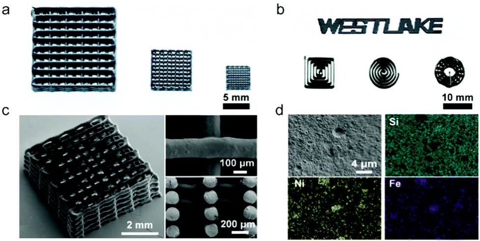
As a first demonstration, a series of microperiodic 3D scaffolds was patterned by extruding permalloy/PDMS nanocomposite inks through nozzles with different inner diameters of 510, 250, and 160 μm (Fig. 3a). The centre-to-centre distance between adjacent filaments was set to be 4 times the nozzle diameter. Next, a 2D motif of “WESTLAKE” and three representative 3D scaffolds were successfully printed with a 160 μm nozzle (Fig. 3b). Fig. 3c shows the scanning electron microscopy (SEM) images of a permalloy/PDMS scaffold with a feature size of 160 μm. The SEM-energy dispersive X-ray spectroscopy (SEM-EDS) images show the Si, Ni and Fe elemental distributions in the cross-section of the filaments, showing the overall uniform distribution of the permalloy nanoparticles. Nevertheless, some aggregations of the permalloy nanoparticles were found, which could explain the small difference between the measured and the calculated permeability by the effective medium theory, where the magnetic nanoparticles were assumed to be uniformly distributed in the PDMS matrix.
 |
| | Fig. 3 (a) Optical images of 10-layer 3D scaffolds assembled from permalloy/PDMS ink printed through nozzles with inner diameters of 500, 210, and 160 μm, respectively (from left to right). (b) Optical images of a 2D pattern and various 3D structured permalloy/PDMS scaffolds assembled using a 210 μm nozzle. (c) Low-magnification SEM images of the permalloy/PDMS scaffold with a feature size of 160 μm (inset: top surface and cross-sectional part). (d) High-magnification SEM image and EDS map scanning of the cross-section of the rod. | |
To demonstrate the high-resolution multimaterial 3D printing of electromagnetic structures, a three-step DIW process was demonstrated using a solenoidal inductor integrated with a magnetic core as an exemplar (see Fig. 4a and Movie S1, ESI†). In the first step, the silver nanoparticle ink is extruded through a 20 μm glass microcapillary nozzle to form a series of parallel lines on a glass substrate, followed by printing of the magnetic nanocomposite ink using a 160 μm steel nozzle above the printed silver lines. Finally, conductive coils were drawn by printing semicircles of silver nanoparticle ink connecting with the underlying lines to form the complete solenoidal inductors. The printed inductors were then thermally annealed at 300 °C to render the printed silver inks conductive. The SEM images of the overall printed device structure are presented in Fig. 4b.
 |
| | Fig. 4 (a) Schematic diagram of the multimaterial printing process of a solenoidal inductor with a magnetic core. (b) SEM images and elemental mapping images of the 3D printed inductor (scale bar: 100 μm). | |
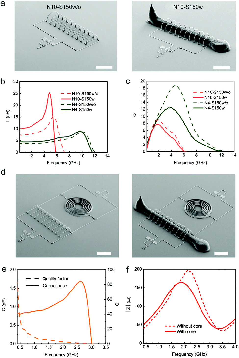
Next, we fabricated a series of solenoidal inductors with varying coil turns (N) and spacing between adjacent coils (S), as well as with (w) and without (w/o) the magnetic core (Fig. 5a and Fig. S2, ESI†) (e.g., N10–S150w/o: N = 10, S = 150 μm, without the magnetic core). Each solenoidal inductor was printed together with a group of ground-signal-ground (GSG) pads for probe station measurement. The inductance (L) of the printed inductors as a function of frequency shows a self-resonance frequency in excess of 5 GHz (Fig. 5b). The integration of a magnetic core into the inductor significantly improves the maximum L from 14 to 25 nH (N = 10, Fig. 5b), despite suffering from a slight loss in quality factor (Q) (Fig. 5c). With fewer coil turns (N = 4), the working frequency of the printed solenoidal inductors was extended up to 11.5 GHz. More details on a comparison with published literature reports are listed in Table S2, ESI.†
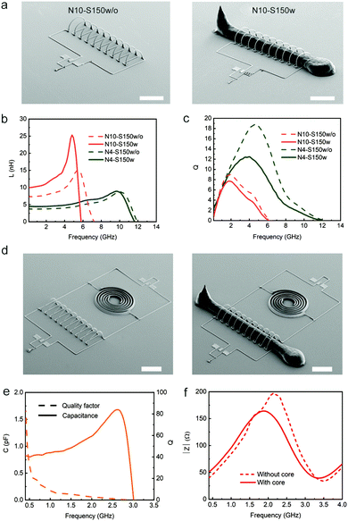 |
| | Fig. 5 (a) SEM images of DIW-printed air-core (left) and magnetic-core inductors (right). (b and c) The corresponding inductance, L, and quality factor, Q, of the printed inductors as a function of frequency. (d) SEM images of the LC resonator consisting of a parallel-plate capacitor and either an air-core (left) or a magnetic-core (right) inductor. (e) Capacitance of the parallel-plate capacitor as a function of frequency. (f) Magnitude of impedance of the LC resonator as a function of frequency (scale bar: 400 μm). | |
As a final demonstration, we printed LC resonators by parallelly connecting a parallel-plate capacitor (area = 0.34 mm2, height = 60 μm, conductor–conductor spacing = 50 μm) and a solenoidal inductor (N10–S150w or N10–S150w/o), as shown in Fig. 5d. The capacitance (C) of the printed parallel-plate capacitors reached the maximum value of 1.75 pF at 2.6 GHz (Fig. 5e). As an increase of inductance L would result in a decrease in the magnitude of the impedance, |Z|, and the resonance frequency, f0, following the relationship below:43
| |  | (6) |
| |  | (7) |
we observed a decrease of |
Z| from 200 to 160 Ω and a decrease of
f0 from 2.3 to 1.7 GHz when a magnetic core was included.
Conclusions
In summary, a permalloy/PDMS nanocomposite magnetic ink was developed for high-resolution DIW. PDMS is introduced as a matrix material both to improve the printability of the inks and extend the operational frequency of the magnetic nanocomposite. We next demonstrated a facile manufacturing route for 3D magnetic-core solenoidal inductors via multimaterial DIW of magnetic permalloy/PDMS together with a conductive silver nanoparticle ink. The addition of the magnetic core significantly increases the inductance of the solenoidal inductors. Thanks to this new functional ink development, our demonstrated 3D multimaterial DIW will establish a new platform for high performance passive RF device design and will lead to new internet of things (IoTs) applications including robotics, personal electronics, and medical devices with high speed data communication capabilities.
Experimental
The details of the ink synthesis, characterization and 3D printing processes are described in the ESI.†
Conflicts of interest
There are no conflicts to declare.
Acknowledgements
The authors are grateful for the financial support of this research by the National Natural Science Foundation of China (No. 51905446). The authors would like to acknowledge funding support from the Westlake University and Bright Dream Joint Institute for Intelligent Robotics.
Notes and references
- F. Garnier, R. Hajlaoui, A. Yassar and P. Srivastava, Science, 1994, 265, 1684–1686 CrossRef CAS
 .
.
- J. H. Holtz and S. A. Asher, Nature, 1997, 389, 829–832 CrossRef CAS .
- B. A. Ridley, B. Nivi and J. M. Jacobson, Science, 1999, 286, 746–749 CrossRef CAS .
- H. Sirringhaus, T. Kawase, R. Friend, T. Shimoda, M. Inbasekaran, W. Wu and E. Woo, Science, 2000, 290, 2123–2126 CrossRef CAS .
- B. K. Tehrani, B. S. Cook and M. M. Tentzeris, IEEE Antennas Wirel. Propag. Lett., 2015, 15, 143–146 Search PubMed .
- G. McKerricher, J. G. Perez and A. Shamim, IEEE Trans. Electron Devices, 2015, 62, 1002–1009 CAS .
- A. Bisognin, J. Thielleux, W. Wei, D. Titz, F. Ferrero, P. Brachat, G. Jacquemod, H. Happy and C. Luxey, IEEE Antennas Wirel. Propag. Lett., 2014, 13, 435–438 Search PubMed .
- H. Subbaraman, D. T. Pham, X. Xu, M. Y. Chen, A. Hosseini, X. Lu and R. T. Chen, IEEE Antennas Wirel. Propag. Lett., 2013, 12, 170–173 Search PubMed .
- J. R. Corea, A. M. Flynn, B. Lechêne, G. Scott, G. D. Reed, P. J. Shin, M. Lustig and A. C. Arias, Nat. Commun., 2016, 7, 1–7 Search PubMed .
- A. E. Ostfeld, I. Deckman, A. M. Gaikwad, C. M. Lochner and A. C. Arias, Sci. Rep., 2015, 5, 15959 CrossRef CAS .
- A. Martínez-Olmos, J. Fernández-Salmerón, N. Lopez-Ruiz, A. Rivadeneyra Torres, L. Capitan-Vallvey and A. Palma, Anal. Chem., 2013, 85, 11098–11105 CrossRef .
- H. Kang, H. Park, Y. Park, M. Jung, B. C. Kim, G. Wallace and G. Cho, Sci. Rep., 2014, 4, 5387 CrossRef CAS .
- L. Hirt, A. Reiser, R. Spolenak and T. Zambelli, Adv. Mater., 2017, 29, 1604211 CrossRef .
- C. Kim, B. Y. Ahn, T. S. Wei, Y. Jo, S. Jeong, Y. Choi, I. D. Kim and J. A. Lewis, ACS Nano, 2018, 12, 11838–11846 CrossRef CAS .
- T. S. Wei, B. Y. Ahn, J. Grotto and J. A. Lewis, Adv. Mater., 2018, 30, 1703027 CrossRef .
- E. B. Duoss, M. Twardowski and J. A. Lewis, Adv. Mater., 2007, 19, 3485–3489 CrossRef CAS .
- A. D. Valentine, T. A. Busbee, J. W. Boley, J. R. Raney, A. Chortos, A. Kotikian, J. D. Berrigan, M. F. Durstock and J. A. Lewis, Adv. Mater., 2017, 29, 1703817 CrossRef .
- J. T. Muth, D. M. Vogt, R. L. Truby, Y. Menguc, D. B. Kolesky, R. J. Wood and J. A. Lewis, Adv. Mater., 2014, 26, 6307–6312 CrossRef CAS .
- J. N. Hanson Shepherd, S. T. Parker, R. F. Shepherd, M. U. Gillette, J. A. Lewis and R. G. Nuzzo, Adv. Funct. Mater., 2011, 21, 47–54 CrossRef CAS .
- H. Yuk, B. Lu, S. Lin, K. Qu, J. Xu, J. Luo and X. Zhao, Nat. Commun., 2020, 11, 1604 CrossRef CAS .
- N. Zhou, C. Liu, J. A. Lewis and D. Ham, Adv. Mater., 2017, 29, 1605198 CrossRef .
- Y. Gu, D. Park, D. Bowen, S. Das and D. R. Hines, Adv. Mater. Technol., 2019, 4, 1800312 CrossRef .
- D. S. Gardner, G. Schrom, F. Paillet, B. Jamieson, T. Karnik and S. Borkar, IEEE Trans. Magn., 2009, 45, 4760–4766 Search PubMed .
- V. Chaudhary, S. A. Mantri, R. V. Ramanujan and R. Banerjee, Prog. Mater. Sci., 2020, 114, 100688 CrossRef CAS .
- M. Vaseem, F. A. Ghaffar, M. F. Farooqui and A. Shamim, Adv. Mater. Technol., 2018, 3, 1700242 CrossRef .
- A. Hodaei, O. Akhlaghi, N. Khani, T. Aytas, D. Sezer, B. Tatli, Y. Z. Menceloglu, B. Koc and O. Akbulut, ACS Appl. Mater. Interfaces, 2018, 10, 9873–9881 CrossRef CAS .
- E. Peng, X. Wei, T. S. Herng, U. Garbe, D. Yu and J. Ding, RSC Adv., 2017, 7, 27128–27138 RSC .
- J. Park, K. Rhee and S. Park, Appl. Surf. Sci., 2010, 256, 6945–6950 CrossRef CAS .
- H. Yun, X. Liu, T. Paik, D. Palanisamy, J. Kim, W. D. Vogel, A. J. Viescas, J. Chen, G. C. Papaefthymiou and J. M. Kikkawa, ACS Nano, 2014, 8, 12323–12337 CrossRef CAS .
-
J. Y. Park and M. G. Allen, A comparison of micromachined inductors with different magnetic core materials, 1996 Proceedings 46th Electronic Components and Technology Conference, IEEE, Orlando, FL, USA, 1996.
- C. S. Smith, S. Savliwala, S. C. Mills, J. S. Andrew, C. Rinaldi and D. P. Arnold, J. Magn. Magn. Mater., 2020, 493, 165718 CrossRef CAS .
-
S. Goldman, Characterization of NiFe/SiO2 multilayers for on-wafer inductors operating at radio and low GHz frequencies, APS March Meeting 2020, Bulletin of the American Physical Society, 2020.
-
J. Salvia, J. A. Bain and C. P. Yue, Tunable on-chip inductors up to 5 GHz using patterned permalloy laminations, IEEE International Electron Devices Meeting, IEDM Technical Digest, 2005.
- T. Dastagir, W. Xu, S. Sinha, H. Wu, Y. Cao and H. Yu, Appl. Phys. Lett., 2010, 97, 162506 CrossRef .
-
Y. Yan, L. Liu, C. Ding, L. Nguyen, J. Moss, Y. Mei and G. Q. Lu, Additive manufacturing of magnetic components for heterogeneous integration, Proceedings of the 2017 IEEE 67th Electronic Components and Technology Conference, IEEE, Orlando, FL, USA, 2017.
- R. Wang, W. Yang, S. Gao, X. Ju, P. Zhu, B. Li and Q. Li, J. Am. Ceram. Soc., 2019, 102, 4688–4697 CrossRef CAS .
- R. Wang, W. Yang, S. Gao, X. Ju, P. Zhu, B. Li and Q. Li, J. Mater. Chem. C, 2019, 7, 8185–8191 RSC .
- B. Feng, R. Hong, L. Wang, L. Guo, H. Li, J. Ding, Y. Zheng and D. Wei, Colloids Surf., A, 2008, 328, 52–59 CrossRef CAS .
- L. Li, G. Li, R. L. Smith and H. Inomata, Chem. Mater., 2000, 12, 3705–3714 CrossRef CAS .
- J. Zhan, C. Yang, X. Wang, Q. Fang, Z. Shi, Y. Yang, T.-L. Ren, A. Wang, Y. Cheng and L. T. Liu, Sens. Actuators, A, 2013, 195, 231–238 CrossRef CAS .
- L. Qiao, F. Wen, J. Wei, J. Wang and F. Li, J. Appl. Phys., 2008, 103, 063903 CrossRef .
- A. D. Podoltsev, I. N. Kucheryavay and B. B. Lebedev, IEEE Trans. Magn., 2003, 39, 539–548 CrossRef .
-
T. H. Lee, The design of CMOS radio-frequency integrated circuits, Cambridge University Press, London, 2003 Search PubMed .
Footnotes |
| † Electronic supplementary information (ESI) available. See DOI: 10.1039/d0tc03244a |
| ‡ Qikun Shi and Hehao Chen contributed equally to this work. |
|
| This journal is © The Royal Society of Chemistry 2020 |
Click here to see how this site uses Cookies. View our privacy policy here. 
 *a and
Nanjia
Zhou
*a and
Nanjia
Zhou