
Triple-junction all-perovskite solar cells: a review
Jialun Zhang
a,
Zijie He
a and
Cong Chen
 *ab
*ab
aState Key Lab of Intelligent Power Distribution Equipment and System, School of Materials Science and Engineering, Hebei University of Technology, Tianjin 300401, China. E-mail: chencong@hebut.edu.cn
bMacao Institute of Materials Science and Engineering (MIMSE), Faculty of Innovation Engineering, Macau University of Science and Technology, Taipa, Macao 999078, China
First published on 12th July 2025
Abstract
Triple-junction all-perovskite solar cells (TJPSCs) use three layers of perovskite materials with different bandgaps to absorb a broader range of the solar spectrum, improving power conversion efficiency (PCE). Currently, the PCE of TJPSC has exceeded 26%, accompanied by an open circuit voltage exceeding 3 V, but there is still a significant gap from the theoretical maximum efficiency of 45%. This paper reviews the working principles and key parameters of TJPSCs and presents recent research progress, with a focus on how component optimization, interface engineering, and charge transport layer improvements influence device efficiency. It also emphasises the essential role of theoretical simulations in guiding bandgap matching, current matching, and energy loss analysis. The paper systematically summarises the advancements made by various research groups from 2019 to 2025, which have contributed to material innovation, fabrication techniques, and device architecture improvements, highlighting notable gains in power conversion efficiency. Although challenges remain in achieving long-term stability and scaling up production, the commercial potential of TJPSCs continues to grow as efforts to optimize material composition, structural design, and manufacturing processes advance.
 Jialun Zhang | Jialun Zhang is a master student at Hebei University of Technology, and a member of Dr Chen's group. He focuses on improving the efficiency and stability of perovskite solar cells by passivating the bulk defects of perovskites. |
 Zijie He | Zijie He is currently a senior student at the collage of Materials Science and Engineering, Hebei University of Technology. He is part of the research group working under Dr Chen to enhance the efficiency and stability of perovskite solar cells. |
 Cong Chen | Cong Chen is a professor and doctoral supervisor at Hebei University of Technology. He obtained his PhD from Jilin University. His research focuses on photovoltaic and optoelectronic integrated devices, including novel solar cells, near-infrared (NIR) photodetectors, and third-generation semiconductor power devices. |
1. Introduction
Perovskite solar cells (PSCs) have emerged as a promising technology in the photovoltaic field in recent years, attracting widespread attention due to their excellent power conversion efficiency (PCE), low cost, and flexibility.1–3 The core material of PSCs is a photovoltaic material with a perovskite crystal structure, typically an organic–inorganic halide perovskite (such as lead-based perovskites or perovskite compounds). These materials exhibit excellent light absorption properties, high electron mobility, and a relatively low bandgap, enabling efficient absorption of sunlight and its effective conversion into electrical energy.4–6 Although single-junction solar cells play a key role in photovoltaic technology, their development faces the following challenges: one major limitation is the fixed bandgap of a single material, which restricts the efficient utilization of the solar spectrum. As a result, high-energy photons lose excess energy as heat, while low-energy photons cannot be absorbed at all.7 Moreover, according to the Shockley–Queisser limit, the theoretical maximum efficiency of a single-junction solar cell is limited to approximately 33.7%.8,9While laboratory results show promising efficiencies, in practical applications, their PCE is often even lower. Additionally, these devices are highly sensitive to temperature variations; under high-temperature conditions, the open-circuit voltage (VOC) decreases, leading to a reduction in overall efficiency.10,11 The most effective way to overcome the efficiency limitations of single-junction solar cells and to make better use of the solar spectrum is to employ multi-junction PSCs.12 In this approach, solar cells are stacked in order of decreasing bandgap, with the subcell having the largest bandgap positioned at the top.13 This design allows the top wide-bandgap perovskite layer to absorb high-energy photons that match its bandgap, while lower-energy photons can pass through and be absorbed by the underlying narrow-bandgap perovskite layers. This not only reduces thermal losses but also enables more effective utilization of the solar spectrum. Multi-junction PSCs have garnered significant attention due to their remarkable potential for high efficiency and may even surpass traditional crystalline silicon solar cells.14 With continuous advancements in material development, structural optimization, and fabrication techniques, the efficiency and stability of multi-junction PSCs are anticipated to be substantially enhanced.15–17
Although traditional multi-junction solar cells based on III–V semiconductor materials offer high efficiency, their use of deposition techniques—such as metal–organic chemical vapor deposition,18 hydride vapor phase epitaxy,19 or molecular beam epitaxy20—results in high production costs, which limits their large-scale application.21 Therefore, developing high-efficiency and low-cost sub-cells has become particularly important. In this regard, metal halide perovskites have emerged as one of the most promising candidate materials due to their high absorption coefficient, long carrier lifetime, and other advantages.22 Moreover, their low cost and ease of fabrication have led to their widespread application in multi-junction architectures. In tandem solar cells, perovskite/silicon solar cells currently hold the record for the highest efficiency.23
By increasing the number of sub-cells to three, a wider spectrum of sunlight can be harnessed, paving the way for further improvements in PCE. However, compared to tandem PSCs, research on triple-junction structures is still in its early stages. Depending on the choice of the bottom cell, three types of perovskite-based triple-junction solar cells have been reported to date: (I) perovskite/perovskite/perovskite (referred to as all-perovskite), (II) perovskite/perovskite/silicon, and (III) perovskite/perovskite/organic solar cells. Among these, the reported PCE for TJPSCs is 26.24%,73 for perovskite/perovskite/silicon is 22.2%, and for perovskite/perovskite/organic solar cells is 19.4%.14
Compared with perovskite/perovskite/silicon and perovskite/perovskite/organic configurations, TJPSCs demonstrate superior integration through a unified material system that enhances compatibility and simplifies processing.24 Since all three sub-cells are composed of perovskite materials, TJPSCs allow greater flexibility in bandgap engineering, where tunable energy levels enable more effective spectral utilization. This structure also facilitates interface alignment and coordinated charge transport, which promote efficient charge separation and extraction and contribute to improved overall device performance. Perovskite materials offer widely tunable bandgaps that allow TJPSCs to approach or even exceed the theoretical efficiency limits of their heterogeneous counterparts. From the fabrication perspective, TJPSCs are compatible with low-temperature, solution-based thin-film deposition methods that reduce energy consumption and production costs in comparison with silicon-based cells, which require high-temperature processing. These techniques also enable integration on flexible substrates and large areas.25 In contrast to organic bottom cells, perovskite absorbers exhibit higher absorption coefficients, better charge mobility, and enhanced photostability, which lead to higher PCE and longer operational lifetime.14,26
TJPSCs represent an emerging solar cell technology that integrates the principles of multi-junction solar cells with those of all-perovskite architectures.27 It is composed of three stacked perovskite layers, each with a different light absorption spectrum, and each perovskite material efficiently absorbs and converts light at different wavelengths. With this structure, TJPSCs can more effectively utilize the different wavelengths of light in the solar spectrum, thereby improving overall PCE. In recent years, TJPSCs have gradually become the focus of research. (The efficiency trends of TJPSCs in recent years are shown in Fig. 1).
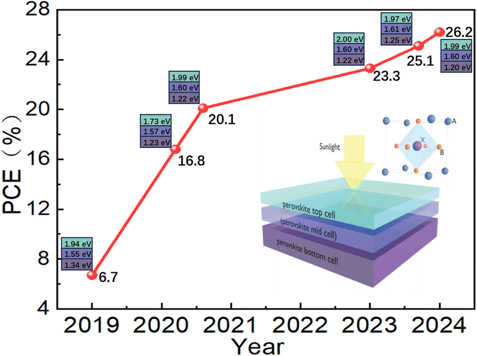 | ||
| Fig. 1 Efficiency of TJPSCs from 2019 to 2025. Reproduced with permission from ref. 28–33 and 70. Copyright 2017, Wiley-VCH. Copyright 2019, Elsevier. Copyright 2020, American Chemical Society. Copyright 2020, Nature. Copyright 2023, Nature. Copyright 2023, Nature. Copyright 2024, Elsevier. | ||
2. The working principle of TJPSCs
2.1 The working principle of PSCs
Metal halide perovskites exhibit excellent optoelectronic properties, such as long carrier diffusion lengths, tunable bandgaps, and high absorption coefficients.34,35 This has become an important material in optoelectronic fields such as solar cells and light-emitting diodes. Metal halide perovskites typically have an ABX3 crystal structure. Many compounds with the chemical formula ABX3 often possess this structure, where A represents a monovalent ion, such as methylammonium (MA+), formamidinium (FA+), or cesium (Cs+), B is a divalent metal cation, such as lead(II) ion (Pb2+) or tin(II) ion (Sn2+), and X represents a halide anion, such as I−, Br−, or the less commonly seen Cl−.36PSCs can be classified into n–i–p (electron transport layer (ETL) deposited first) and p–i–n (hole transport layer (HTL) deposited first) device structures based on the order of deposition of the electron (n) and hole (p) transport layers and the perovskite absorber (i) layer.37 The matching and alignment of their bandgaps depend on the energy levels, electron affinity, and ionization potential of the materials. Generally, materials with lower electron affinity and ionization potential are used as HTLs, while materials with higher electron affinity and ionization potential are used as ETLs.38–40 In PSCs, the HTL typically uses materials with electron-blocking properties. Its primary function is to assist in hole injection from the perovskite active layer and effectively transport these holes to the back electrode. Additionally, the HTL can also act as an electron-blocking layer, preventing electron flow from entering this layer.38,41,42 In inorganic materials, copper iodide (CuI) is commonly used in PSCs due to its high hole mobility and stability, providing excellent charge transport properties. Nickel oxide (NiOx) is also a common inorganic hole transport material, with good hole conductivity and appropriate energy level alignment, enabling efficient hole transport to the electrode. Additionally, poly(3,4-ethylene dioxythiophene-phenylamine) (PTAA), an organic polymer material, is widely used in PSCs due to its good hole conductivity and suitable energy level structure, effectively enhancing the device's efficiency and stability.43
The ETL is an essential component for PSCs, as it transports electrons from the perovskite active layer to the front electrode. At the same time, the ETL can act as a hole-blocking layer, preventing holes from entering the front electrode, thereby avoiding unnecessary charge losses.38,44 Zinc oxide (ZnO), [6,6]-phenyl-C60-butyric acid methyl ester (PCBM), and fullerene (C60) are commonly used electron transport materials in PSCs. ZnO has excellent electronic conductivity and tunable optical properties. Although stability issues may arise under certain conditions, it is still widely used in these cells due to its low cost and good electron transport performance.45 PCBM is an organic electron transport material that can effectively facilitate electron transfer, particularly exhibiting outstanding performance in organic–inorganic hybrid structures.46 C60, acting as a classic carbon-based material, also possesses excellent electronic conductivity, enabling efficient electron transport, thereby enhancing the overall performance of solar cells.47
In addition, a complete PSC also includes an anode and a cathode, both of which play crucial roles in charge collection and transport. The anode is responsible for collecting holes generated in the perovskite layer and transferring them to the external circuit via the HTL. Therefore, the anode must possess good electrical conductivity and transparency to allow light to pass through and reach the perovskite layer for effective photoelectric conversion. Commonly used materials for the anode include transparent conductive oxides, such as indium tin oxide (ITO).48,49 The cathode, on the other hand, is responsible for collecting the generated electrons and transferring them to the external circuit through the ETL. Cathode materials are also required to have good electrical conductivity, with common choices including metals such as silver, aluminum, and gold.50 In multi-junction structures, the anode and cathode also need to ensure smooth charge transport between the layers, effectively collecting and transferring electrons and holes, thereby further enhancing the PCE.
2.2 The working principle of TJPSCs
By stacking three perovskite layers with different bandgaps to form a multi-junction structure, as shown in Fig. 2a, it maximizes the absorption of sunlight, thereby further improving the PCE. Its operating principle is based on bandgap tuning and the optimized design of the multilayer structure.51 One of its key features is the precise design of the bandgap for each layer, enabling each layer to be optimized for absorbing light of different wavelengths: the top layer absorbs high-energy short-wavelength light (such as blue and ultraviolet light), the middle layer absorbs medium-energy light (such as green and yellow light), and the bottom layer absorbs lower-energy long-wavelength light (such as red and near-infrared light), as shown in Fig. 2b and c.33 This layered absorption approach allows the TJPSC to fully utilize the entire solar spectrum, overcoming the limitations of single materials in spectral absorption. When light strikes the top perovskite layer of the cell, photons are absorbed, generating electron–hole pairs in each layer of perovskite material.52 Under the influence of the electric field, these charge carriers are effectively separated, with electrons migrating to the transparent electrode (such as ITO), and holes migrating to the metal electrode. The charge transport layers between each layer collect the electrons and holes, ultimately outputting the current to the external circuit. The perovskite layers are connected through junctions or transparent conductive layers to ensure efficient charge transport,53 which reduces losses caused by recombination during the transfer process, thereby enhancing the collection efficiency of photogenerated charges and significantly improving the overall PCE. | ||
| Fig. 2 (a) Schematic diagram of a perovskite-based triple-junction solar cell, showing some common materials used in each layer and their corresponding deposition techniques; (b) and (c) illustrations of the solar spectrum as utilized by triple-junction solar cells. Reproduced from ref. 14 with permission from Royal Society of Chemistry, Copyright 2024. | ||
3. Theoretical simulation analysis of high-efficiency TJPSCs
For high-efficiency TJPSCs, a rational bandgap allocation is a key factor in achieving high performance. Sub-cells with different bandgaps can absorb photons of different energies from the solar spectrum, thereby maximizing photon utilization and optimizing current matching.54 Yang et al. developed a monolithic TJPSC, in which the top and middle perovskite absorber layers were fabricated via thermal co-evaporation, while the bottom absorber layer was prepared using a solution-processing method. By optimizing the thicknesses of each absorber layer through optical simulations, excellent current matching was achieved—9.6 mA cm−2 for the top subcell, 9.3 mA cm−2 for the middle, and 9.0 mA cm−2 for the bottom—resulting in a PCE of 15.77%.55However, the selection of bandgaps requires a balance between spectral absorption, current matching, and energy loss to ensure the overall optimization of PCE.56 In a triple-junction structure, the overall output voltage of the solar cell is further increased by stacking the voltages of each junction. A remarkable feature of metal halide perovskites is their tunable bandgap, which makes them an ideal choice for multijunction solar cells.57 By means such as cation or halide substitution, the bandgap of perovskites can be tuned within the range of 1.2 eV to 3.1 eV, as shown in Fig. 3.
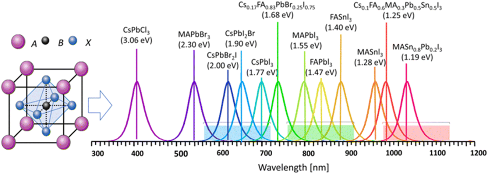 | ||
| Fig. 3 Perovskite materials with the ABX3 structure, where A is a monovalent organic or inorganic cation, such as MA+, FA+, or Cs+. B is typically a divalent metal such as Pb2+ or Sn2+, and X is a halide, mainly I−, Br−, or their combinations. The bandgap of perovskites can be tuned in the range of 1.2 eV to 3.1 eV. Reproduced from ref. 14 with permission from Royal Society of Chemistry, Copyright 2024. | ||
The tunable bandgap of PSCs offers excellent potential for applications in tandem technologies.58–61 In particular, all-perovskite tandem solar cells offer greater potential for performance improvement compared to single-junction devices but require specific engineering optimizations for bandgap matching, which involves the strategic selection and arrangement of light-absorbing materials with different bandgaps in multi-junction solar cells such as TJPSCs, in which the bandgap energies decrease progressively from the top to the bottom sub-cell. In recent years, many studies have demonstrated optimized all-perovskite tandem solar cells with narrow-bandgap sub-cells ranging from 1.21 to 1.26 eV and wide-bandgap sub-cells ranging from 1.73 eV to 1.78 eV could achieve PCE of 26.0% to 28.5%.62–66 However, the bandgaps of current all-perovskite multijunction solar cells have not yet reached their optimal values, which will be a key issue for future research.
In addition, the optimum bandgap pairs for middle and top cells to maximize PCE in each structure is given in Table 1.
| Bottom cell (eV) | Middle cell (eV) | Top cell (eV) |
|---|---|---|
| 1.00 | 1.42 | 1.94 |
| 1.10 | 1.49 | 2.00 |
| 1.20 | 1.57 | 2.06 |
| 1.30 | 1.66 | 2.13 |
Similar to the experimental validations conducted by Eperon and Leijtens, the bandgap range of the bottom perovskite absorber layer is 0.9–1.35 eV, while that of the top perovskite absorber layer is 1.5–2 eV. The simulated all-perovskite triple-junction structure is based on a tandem architecture, with an additional wide-bandgap top perovskite absorber layer added, having a bandgap range of 1.9–2.3 eV. The middle perovskite absorber layer has a bandgap range of 1.5–1.9 eV, while the bottom perovskite absorber layer maintains a bandgap of 1.22 eV, which is currently the lowest reported bandgap among high-efficiency PSCs.67
S. Hussain et al. modelled and optimized single-junction, tandem, and triple-junction PSCs using the SunSolve simulation tool. The simulations were based on thin-film optics and the Monte Carlo ray tracing (MRT) method, primarily to analyze optical losses in different layers. During the optimization process, the researchers adjusted the thickness of each layer step-by-step to maximize the PCE, while taking into account reflection losses, parasitic absorption losses, and optical gains. In the TJPSC, the structure consists of three sub-cells with bandgaps of 1.94 eV (top), 1.55 eV (middle), and 1.22 eV (bottom), respectively, and ITO was used as the recombination layer to facilitate charge recombination. Ultimately, the study suggested that for achieving ultra-high efficiency in all-perovskite multi-junction solar cells, the top sub-cell should have a bandgap of 1.8–1.9 eV, and the bottom sub-cell should have a bandgap of approximately 1.22 eV with a thickness of around 1 micron.68
At present, the bottom sub-cell bandgaps of TJPSCs have adopted values of 1.22 eV and 1.25 eV. In TJPSCs, the schematic diagram of photon energy absorption by wide-bandgap and narrow-bandgap perovskites, as shown in Fig. 4a, along with the spectral irradiance chart, indicates that when the narrow bandgap is 1.22 eV, the theoretical maximum PCE of the triple-junction solar cell corresponds to a specific range of bandgaps, as shown in Fig. 4b. In the theoretical calculation of the PCE limit, Jaekeun Lim et al. found that when the bottom sub-cell bandgap is set to 1.22 eV, a combination of middle sub-cell bandgaps ranging from 1.59 eV to 1.61 eV, and wide bandgaps ranging from 2.08 eV to 2.11 eV, can achieve a PCE exceeding 46%, as shown in Fig. 4c. When the bottom sub-cell bandgap is set to 1.25 eV, a combination of middle sub-cell bandgaps ranging from 1.62–1.65 eV and wide bandgaps ranging from 2.1–2.13 eV can theoretically achieve a PCE over 45% under AM 1.5G illumination, as shown in Fig. 4d.26
 | ||
| Fig. 4 (a) Schematic illustration of photon energy absorption by wide-bandgap and narrow-bandgap perovskites in a triple-junction structure; (b) spectral irradiance chart showing the bandgap range corresponding to the theoretical maximum PCE of a triple-junction cell with a narrow bandgap of 1.22 eV; (c) theoretical efficiency limit of monolithic triple-junction solar cells considering a fixed narrow bandgap of 1.22 eV, with the middle bandgap ranging from 1.3–1.7 eV and the wide bandgap from 1.7–2.2 eV; (d) theoretical efficiency limit of monolithic triple-junction solar cells considering a fixed narrow bandgap of 1.25 eV, with the middle bandgap ranging from 1.3–1.7 eV and the wide bandgap from 1.7–2.2 eV. Reproduced from ref. 26 with permission from Royal Society of Chemistry, Copyright 2024. | ||
N. Shrivastav et al.70 explored the optimized design and simulation of TJPSC using the SCAPS-1D tool.69 As shown in Fig. 5a, incorporating a two-step filtered spectrum and current-matching technique to enhance device performance. They first calculated the filtered spectra entering the middle and bottom sub-cells after passing through the top sub-cell and optimized the current-matching points of each sub-cell to maximize energy utilization. The final current-matching curve was obtained by adjusting the thicknesses of the top, middle, and bottom sub-cells, as shown in Fig. 5b. The optimized cell achieved a PCE of 26.24%, as shown in Fig. 5c, with VOC of 3.76 V, a short-circuit current density (JSC) of 10.70 mA cm−2, and an FF of 69%. This work achieved enhanced PCE by optimizing the filtered spectra and current matching, demonstrating that the proposed method can be applied to developing high-efficiency tandem solar cells and providing crucial theoretical support for further optimization of photovoltaic devices.
 | ||
| Fig. 5 (a) Layer structure of the sub-cells in the triple-junction all-PSC; (b) final current-matching curve obtained from the variation in the thicknesses of the top, middle, and bottom sub-cells; J–V curve obtained through current matching of the top, middle, and bottom sub-cells with different thicknesses; (d) diagram of the simulation and optimization strategy; (e) absorption and current analysis of the optimized internal layers (current losses due to parasitic absorption and reflection), with the bandgaps of the perovskite absorber layers being 2.26 eV, 1.64 eV, and 1.22 eV; (f) heat map showing the PCE of the optimized TJPSC under different conditions, with the FF held constant at 81.1%. Reproduced with permission from ref. 70 and 73. Copyright 2024, Elsevier. Copyright 2024, The Optical Society. | ||
Mohamed Hussein et al.73 conducted a study using an internally developed energy yield (EY) simulation tool, EYcalc,71 as shown in Fig. 5d, to optimize the performance of TJPSCs under realistic illumination conditions. The simulation was first validated against existing experimental data, and a hybrid optimization algorithm combining Particle Swarm Optimization and Gravitational Search Algorithm (PSOGSA)72 was employed to identify the optimal perovskite bandgap combinations and layer thicknesses. The optimal perovskite layer thicknesses were determined to be 828 nm, 822 nm, and 1000 nm for the top, middle, and bottom sub-cells, respectively. Additionally, absorption and current loss analyses were performed for each layer of the optimized TJPSC. It was found that parasitic absorption and reflection caused certain current losses, as shown in Fig. 5e, with the band gaps of the perovskite absorber layers being 2.26 eV, 1.64 eV, and 1.22 eV, respectively. Under standard test conditions, the optimized solar cell achieved a PCE of 27.1%, which was further improved to 36% through electrical optimization, as shown in Fig. 5f.
Maximilian T. Hörantner et al.75 combined optical and electrical models using the transfer matrix method74 to simulate light absorption and interference effects. They constructed a single-diode model based on experimental data (refractive index, bandgap, J–V curves), considering loss factors such as non-radiative recombination and series resistance. To optimize the bandgap and thickness, they adjusted the perovskite layer bandgap (1.2–2.3 eV) and thickness (with the bottom perovskite layer thickness reaching 1.5 μm) to match the current and maximize the voltage. Furthermore, the researchers assessed the performance feasibility of all-perovskite double-junction, triple-junction, and perovskite–perovskite–silicon triple-junction solar cells. Based on the current state-of-the-art PSC parameters and design constraints, the PCE of all-perovskite double-junction solar cells could approach 32%, all-perovskite triple-junction solar cells could reach 33%, and perovskite–perovskite–silicon triple-junction solar cells could exceed 35%. Additionally, the study proposed ways to enhance light capture, demonstrating that through further improvements, the efficiencies of these three structures could be increased to 33%, 37%, and 39% (Fig. 6), respectively. Therefore, compared to single-junction and double-junction cells, triple-junction perovskite cells offer higher PCE and theoretical efficiency limits.
 | ||
| Fig. 6 Optimized performance of all-perovskite double-junction (a and d), all-perovskite triple-junction (b and e), and perovskite–perovskite–silicon (c and f) solar cells under ideal bandgap combinations and optically idealized thickness constraints. Reproduced from ref. 75 with permission from American Chemical Society, Copyright 2017. | ||
4. Optimization of TJPSCs
4.1 Optimization of perovskite sub-cell components
With the continuous development of photovoltaic technology, TJPSCs are considered an effective way to enhance PCE due to their ability to absorb light over a wider spectral range efficiently. Compared to traditional single-junction solar cells, triple-junction cells achieved enhanced PCE by combining multiple material layers with matched energy band structures.76 Perovskite materials, with their excellent optoelectronic properties and tunable bandgaps, have become the core components in TJPSCs.77 However, despite the enormous potential of perovskite materials in enhancing efficiency, their stability, charge carrier transport properties, and light absorption characteristics in practical applications still require further optimization. Especially in multi-junction solar cells, the optimization of the perovskite layer composition is crucial,78 as it not only affects the overall PCE of the cell but also relates to the compatibility and stability between different layers. Therefore, optimizing the chemical composition, structural design, and thin-film fabrication processes of perovskite materials to improve the performance and stability of TJPSCs is of utmost importance.In 2019, McMeekin et al. fabricated the first solution-processed all-perovskite tandem and triple-junction solar cells. The triple-junction solar cell adopted an n–i–p structure, with perovskite light-absorbing layers including 1.94 eV-FA0.83Cs0.17Pb(Br0.7I0.3)3,1.55 eV-MAPbI3, and 1.34 eV-MAPb0.75Sn0.25I3.33 This study remains the only one to date that employs an n–i–p architecture for TJPSCs. The device fabrication method is also unique; all layers of the cell, except for the silver electrode, were manufactured using solution-processing techniques, including the typically sputtered ITO composite layer, which was instead deposited using spin-coating of ITO nanoparticles. To address solvent compatibility issues, the researchers replaced the traditional dimethylformamide/dimethyl sulfoxide solvent system with a novel acetonitrile/methylamine system for the low and mid-bandgap perovskites. By adjusting the content of the metal cations at the B site, they achieved sequential deposition of the low and mid-bandgap perovskite light-absorbing layers on the bottom perovskite device. However, the change in the solvent system led to a decrease in PCE. By combining 1.94 eV-FA0.83Cs0.17Pb(Br0.7I0.3)3 with 1.57 eV-MAPbI3, researchers achieved a two-terminal tandem PSC with a steady-state PCE of 15.2%. In addition, they demonstrated the fabrication of a 1.34 eV-MAPb0.75Sn0.25I3 narrow-bandgap perovskite absorber using an acetonitrile/methylamine solvent system. This marked the first demonstration of a monolithic TJPSC, achieving a VOC of 2.83 V. The performance of the device was mainly limited by the low JSC of the bottom solar cell with the narrow bandgap (only 8.3 mA cm−2), as well as a relatively low fill factor (FF) of 43.0%. As a result, the device did not reach its optimal performance, yielding a PCE of only 6.7%, as shown in Fig. 7b. Nevertheless, modelling predicts that triple-junction PSCs fabricated by this method could potentially achieve a PCE of up to 26.7%.
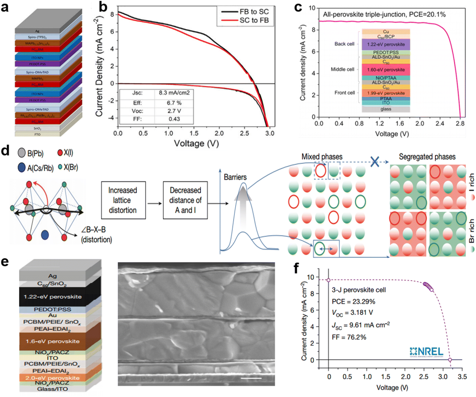 | ||
| Fig. 7 (a) Device architecture of the TJPSC and its J–V curve measured at a scan rate of 0.25 V s; (b and c) J–V curves of TJPSC; (d) schematic illustration of the light-induced phase separation suppression mechanism, where hollow circles represent vacancies; (e) device structure and SEM image of the TJPSC; (f) quasi-steady-state J–V curve of the certified TJPSC by NREL. Reproduced with permission from ref. 30, 31 and 33.Copyright 2019, Elsevier. Copyright 2020, American Chemical Society. Copyright 2023, Nature. | ||
Demonstrating the feasibility of all-perovskite multijunction solar cells, this study offers valuable scientific insights to support future advancements in efficiency and stability. By optimizing the composition of different perovskite materials, researchers successfully fabricated a TJPSC and detailed the key processing techniques involved, particularly the use of the acetonitrile/methylamine solvent system. These technological advancements offer a novel pathway for the fabrication of high-efficiency multijunction solar cells. With further development, these devices are expected to achieve higher efficiency and longer operational lifetimes.
In 2020, Wang et al. reported a universal two-step solution processing method that enabled the fabrication of monolithic TJPSC with a PCE of 16.8%.28 The researchers focused on a mixed perovskite composition: Csz(FA0.66MA0.34)1−zPb1−xSnxI3−y(1−z)Bry(1−z). By adjusting the molar ratios of the precursor solutions, they successfully prepared perovskite films with a wide bandgap 1.73 eV-Cs0.1(FA0.66MA0.34)0.9PbI2Br, a mid-bandgap 1.57 eV-FA0.66MA0.34PbI2.85Br0.15, and a narrow bandgap 1.23 eV- FA0.66MA0.34Pb0.5Sn0.5I3. In the two-step deposition process, inorganic salts (CsI, PbI2, and SnI2) were first dissolved in a mixture of N,N-dimethylformamide (DMF) and dimethyl sulfoxide (DMSO) and spin-coated to form an intermediate precursor film. Subsequently, organic salts (FAI, FABr, MAI, and MABr) dissolved in isopropanol were spin-coated on top, followed by thermal annealing to accelerate the formation of perovskite crystals. Moreover, this approach enabled the fabrication of high-efficiency and reproducible monolithic TJPSC, achieving a PCE of 16.8%, a FF of 81%, and VOC of 2.78 V—only 80 mV lower than the sum of the VOC of the individual sub-cells, indicating low resistive losses. The device exhibited good stability during a 300 second maximum power point tracking measurement. Compared to previous studies, the improved FF was the primary factor contributing to the enhanced PCE. However, the JSC was still limited by the sub-cells. This work introduced a novel method for fabricating high-efficiency all-perovskite tandem solar cells and experimentally validated its effectiveness. Statistical analysis of multiple triple-junction devices demonstrated good reproducibility, which is essential for future commercial production. The findings provide a significant technical foundation for the development of PSC technology and hold promise for substantial breakthroughs in photovoltaic performance.
Insufficient crystallinity can impair the effective filling of the bandgap, thereby reducing the light absorption capability and promoting the formation of interfacial defects and trap states, ultimately degrading device performance.79 Such defects not only act as energy sinks that facilitate non-radiative recombination but also significantly reduce the population of photogenerated charge carriers available for effective collection. Furthermore, low crystallinity impairs charge transport by decreasing electrical conductivity, complicating the internal charge transport pathways, and elevating the likelihood of electron–hole recombination.80 In the same year, Xiao et al. reported a TJPSC with a PCE of 20.1% (the device structure is shown in Fig. 7c (ref. 30)). The perovskite materials employed in the three sub-cells had the following bandgaps and compositions: 1.99 eV- Cs0.2FA0.8PbI0.9Br2.1, 1.60 eV-Cs0.05FA0.95PbI2.55Br0.45, and 1.22 eV-FA0.7MA0.3Pb0.5Sn0.5I3. The researchers aimed to develop a wide-bandgap perovskite material (∼2.0 eV) to match the 1.22 eV rear sub-cell. By employing a one-step anti-solvent method and incorporating 5 mol% Pb(SCN)2 as an additive in the precursor solution, they successfully fabricated wide-bandgap perovskite films with enlarged grain sizes, leading to high-quality PSCs. The resulting device exhibited a PCE of 20.1%, a JSC of 8.8 mA cm−2, VOC of 2.80 V, and an FF of 81.0%. Under a nitrogen atmosphere, the device demonstrated good operational stability during 180 seconds of maximum power point tracking. This work provides important insights into the fabrication of large-grain perovskite films through the anti-solvent method and compositional engineering of precursor solutions, highlighting the critical role of high crystallinity in enhancing PSC performance.
For wide-bandgap iodide/bromide mixed perovskite absorber layers, light-induced phase separation occurring in the top sub-cell of triple-junction solar cells limits both the PCE and operational stability of perovskite-based multijunction photovoltaic devices.81 In 2023, Wang et al. reported the first certified TJPSC.31 In this study, the researchers employed three different perovskite absorber materials: 2.00 eV-Rb0.15Cs0.85PbI1.75Br1.25, 1.60 eV-Cs0.05FA0.90MA0.05Pb(I0.90Br0.10)3, and 1.22 eV-Cs0.05FA0.70MA0.25Pb0.50Sn0.50I3 with 5% SnF2 additive, to fabricate an TJPSC. The certified PCE of the device reached 23.3%, with a JSC of 9.6 mA cm−2, VOC of 3.20 V, and a FF of 76.2%. The encapsulated device retained 80% of its initial efficiency after 450 hours of environmental testing. In this work, the researchers partially substituted Cs+ ions with rubidium (Rb+) ions in the inorganic iodide/bromide mixed perovskite CsPbI1.75Br1.25. Since Rb+ has a smaller ionic radius than Cs+, this substitution increased lattice distortion and reduced the average atomic distance between A-site cations and iodide ions, thereby raising the activation energy barrier for halide ion migration. As a result, the light-induced phase separation phenomenon was effectively suppressed, as shown in Fig. 7d.82 The researchers employed a ∼2.0 eV wide-bandgap Rb/Cs mixed-cation inorganic perovskite as the absorber layer for the top sub-cell and successfully fabricated a TJPSC, achieving a PCE of 24.3% (with a certified PCE of 23.3%) (as shown in Fig. 7f). A key factor contributing to the 23.3% efficiency was the development of a high-bandgap, fully inorganic Rb/Cs perovskite absorber layer, which offered enhanced stability. Moreover, a bilayer structure of NiOx/Me-4PACz was introduced as the HTL) in both the top and middle cells (Fig. 7e). The high VOC of 3.2 V was partially attributed to the high-quality perovskite/charge transport layer interface. Me-4PACz has been demonstrated to form a low-loss interface with perovskite materials.83 In addition, the perovskite/PCBM interface was passivated using phenylethylammonium iodide (PEAI) and ethylenediamine diiodide (EDAI2) to reduce interfacial recombination losses. Polyethylenimine ethoxylated (PEIE) was spin-coated on top of the PCBM layer to protect the underlying structure further.
This section reviews recent advancements in the optimization of sub-cell components in TJPSCs. Key areas of focus include solvent system engineering, control of perovskite crystallinity, interface passivation, and the design of charge transport layers. These efforts provide important technical pathways and theoretical support for the development of high-efficiency and stable multi-junction PSCs.
4.2 Optimization of the interconnection layer in sub-cells of TJPSCs
TJPSCs have emerged as a research hotspot in the photovoltaic field in recent years due to their high PCE and tunable bandgap flexibility. As a key component for achieving high efficiency, the interconnecting layers between sub-cells play a crucial role in facilitating charge transport and suppressing recombination. However, the series-connected architecture of multi-junction devices imposes stringent requirements on the conductivity, energy level alignment, and optical transparency of the ICLs. Therefore, optimizing the design and fabrication of interconnecting layers has become one of the core challenges in improving the efficiency of TJPSCs.84Perovskite thin films typically exhibit rough surfaces, making it challenging to form thin and uniform charge transport layers on top of them after solution processing. This can result in exposed areas and pinholes, which may lead to the formation of shunting paths. Studies have shown that using NiOx alone or in combination with an HTL, can help achieve complete coverage of the perovskite surface. In 2020, Xiao et al. developed and employed a NiOx/PTAA bilayer as the HTL for the middle sub-cell, as shown in Fig. 8a.30 To address the issue of incomplete surface coverage caused by the thin PTAA layer—resulting in discontinuous HTL—researchers first spin-coated a nanocrystalline NiOx film approximately 80 nm thick prior to the deposition of PTAA. During the spin-coating process, the NiOx nanocrystals could partially fill surface grooves, thereby improving the surface roughness and providing a denser and more continuous base for the subsequent PTAA layer. Compared to a single-layer HTL, the bilayer structure offered superior coverage over the rough surface of the preceding sub-cell. By optimizing current matching between sub-cells and simultaneously reducing optical reflection losses, the researchers enhanced the PCE of the all-PSC. The PCE reached up to 20.1% with the NiOx/PTAA bilayer, significantly outperforming the single-layer PTAA configuration, as shown in Fig. 8b. This bilayer strategy had previously been applied in perovskite/CIGS tandem solar cells. Jost et al. used atomic layer deposition to deposit a 10 nm-thick NiOx layer and directly deposited PTAA on top without any further annealing, in order to prevent short-circuiting in perovskite cells fabricated on rough CIGS surfaces.85 It is worth noting that some other perovskite-based triple-junction solar cells have also incorporated NiOx single layers or NiOx-containing bilayer hole transport structures into their device architectures.
 | ||
| Fig. 8 (a) Device architecture of the TJPSC; (b) J–V curves of devices using PTAA and NiOx/PTAA as the HTL; (c) quasi-Fermi level splitting of control and 1 mol% PDA-added perovskite films deposited on glass substrates; (d) schematic illustration of the crystallization process of PDA cations with mixed Br/I perovskite precursors; (e) atomic concentration ratios of halides (Br, I, and Cl) to Pb obtained from XPS depth profiling for the control (solid lines) and PDA-added perovskite films (dashed lines). Vertical lines indicate the interface with the HTL. Reproduced with permission from ref. 30 and 32.Copyright 2020, American Chemical Society. Copyright 2023, Nature. | ||
In 2023, Wang et al. reported a monolithic TJPSC.32 As a p–i–n type device, this cell achieved VOC of 3.33 V and a peak PCE of 25.1%, with a certified efficiency of 23.87%. In this study, the researchers introduced 1 mol% of 1,3-propanediammonium iodide (PDA) as an additive into the perovskite precursor solution and found that the quasi-Fermi level splitting loss at the HTL interface (55 meV) was completely eliminated (Fig. 8c), indicating a lossless HTL interface. By investigating the reduction of defect density and improvement in phase homogeneity of high-bromide-content perovskite films, the study demonstrated the potential of diammonium halide salts to passivate surface defects, as shown in Fig. 8d. PDA not only facilitated better control over film growth and improved halide distribution uniformity, as shown in Fig. 8e, but also contributed to minimizing energy losses.86 The researchers fabricated a monolithic TJPSC using absorber layers with compositions and bandgaps of 1.97 eV-Cs00.15FA0.85Pb(I0.4Br0.6)3, 1.61 eV-Cs0.05FA0.9MA0.05Pb(I0.85Br0.15)3, and 1.25 eV-Cs0.05FA0.7MA0.25Pb0.5Sn0.5I3 for the top, middle, and bottom sub-cells, respectively. Even after 200 hours of continuous maximum power point tracking, the device retained 80% of its initial efficiency. Through bulk and interfacial passivation using this salt, the study significantly suppressed non-radiative recombination both within the perovskite material and at the heterojunction interfaces between the perovskite and charge transport layers. This effectively enhanced both the efficiency and stability of the wide-bandgap bromide-rich PSCs.
The device structures and photovoltaic parameters VOC, JSC, FF and, PCE of the discussed triple-junction all-perovskite solar cells are summarized in Table 2.
| Perovskite top cell | Perovskite middle cell | Perovskite bottom cell | JSC (mA cm−2) | VOC (V) | FF (%) | PCE (%) | Ref. |
|---|---|---|---|---|---|---|---|
| FA0.83Cs0.17Pb(Br0.7I0.3)3 (1.94 eV) | MAPbI3 (1.55 eV) | MAPb0.75Sn0.25I3 (1.34 eV) | 8.3 | 2.70 | 43 | 6.7 | 33 |
| Cs0.1(FA0.66MA0.34)0.9PbI2Br (1.73 eV) | FA0.66MA0.34PbI2.85Br0.15 (1.57 eV) | FA0.66MA0.34Pb0.5Sn0.5I3 (1.23 eV) | 7.4 | 2.78 | 81 | 16.8 | 28 |
| Cs0.2FA0.8PbI0.9Br2.1 (1.99 eV) | Cs0.05FA0.95PbI2.55Br0.45 (1.60 eV) | FA0.7MA0.3Pb0.5Sn0.5I3 (1.22 eV) | 8.8 | 2.8 | 81.1 | 20.1 | 30 |
| CsPbI1.4Br1.6 and Rb0.15Cs0.85PbI1.75 Br1.25 (2.0 eV) | Cs0.05FA0.95PbI2.55Br0.45 (1.60 eV) | FA0.7MA0.3Pb0.5Sn0.5I3 (1.22 eV) | 9.71 | 3.21 | 77.93 | 24.3 | 31 |
| Cs0.15FA0.85Pb(I0.4Br0.6)3 (1.97 eV) | Cs0.05FA0.9MA0.05Pb(I0.85Br0.15)3 (1.61 eV) | Cs0.05FA0.7MA0.25Pb0.5Sn0.5I3(1.25 eV) | 9.7 | 3.33 | 78 | 25.1 | 32 |
5. Conclusion and outlook
The TJPSCs have attracted widespread attention in recent years due to their high PCE and potential for low-cost manufacturing. This review systematically examines the research progress of TJPSCs from 2019 to 2025, including their working principles, theoretical simulations, optimization strategies, and performance characterization. The TJPSC achieves efficient absorption of the solar spectrum through bandgap optimization, which enhances its PCE. Studies show that an appropriate combination of bandgaps (such as 1.22 eV, 1.60 eV, and 2.00 eV) can optimize current matching, reduce energy loss, and improve overall performance. Both theoretical calculations and experimental research indicate that the conversion efficiency of such cells is expected to exceed the Shockley–Queisser limit, with some experiments already achieving over 26% efficiency. Recent research has focused on the fine-tuning of perovskite compositions to improve stability and durability. For instance, Rb/Cs mixed cation perovskites can effectively suppress light-induced phase separation, thereby extending the device lifetime. Moreover, optimizing the electron/HTLs (such as the NiOx/PTAA bilayer structure) could significantly enhance charge transport efficiency, reduce interface defects, and improve the VOC and FF of the device.Further, novel fabrication methods need to be developed to improve film quality, increase device stability, and enhance reproducibility. These methods include spray coating, vacuum flash evaporation, etc. In addition, optimizing the interconnection layers between sub-cells—such as transparent conductive layers and interface modification layers—is critical for enhancing overall performance because of the characteristics of multi-junction structures. Fully utilizing the work function and surface property regulation of self-assembled molecules, coupled with the ALD method for depositing ultra-dense inorganic hole transport materials, such as ALD-NiOx. Most importantly, future research should focus on improving material stability, optimizing bandgap matching, inhibiting phase separation in wide bandgap top cells and ion migration in perovskite materials, and promoting large-area manufacturing to accelerate commercialization. By integrating interdisciplinary research and technological innovation, TJPSCs are expected to become key players in the future photovoltaic market, offering more efficient solutions for the development of renewable energy.
Data availability
The data that support the findings of this study are available from the corresponding author upon reasonable request.Conflicts of interest
The authors declare no competing interests.Acknowledgements
This work was supported by the National Natural Science Foundation of China (52462031, U21A2076), the S&T Program of Hebei (24464401D), the Natural Science Foundation of Hebei Province (E2024202086, E2024202300). The Central Guidance on Local Science and Technology Development Fund of Hebei Province (226Z4305G). Hebei Province Higher Education Science and Technology Research Project (JZX2024030). Shijiazhuang Basic Research Project at Hebei-based Universities (241790847A). Science and Technology Cooperation Special Project of Shijiazhuang (SJZZXC24005).References
- M. A. Green, A. Ho-Baillie and H. J. Snaith, Nat. Photonics, 2014, 8, 506–514 CrossRef CAS
.
- H. S. Jung and N. G. Park, Small, 2015, 11, 10–25 CrossRef CAS PubMed
- N.-G. Park, Mater. Today, 2015, 18, 65–72 CrossRef CAS
- J. H. Heo, S. H. Im, J. H. Noh, T. N. Mandal, C.-S. Lim, J. A. Chang, Y. H. Lee, H.-j. Kim, A. Sarkar, M. K. Nazeeruddin, M. Grätzel and S. I. Seok, Nat. Photonics, 2013, 7, 486–491 CrossRef CAS
- M. Ahmadi, T. Wu and B. Hu, Adv. Mater., 2017, 29, 1605242 CrossRef PubMed
- N.-G. Park, T. Miyasaka and M. Grätzel, Organic–inorganic halide perovskite photovoltaics, Springer, Cham, Switzerland, 2016, pp. 1–366 Search PubMed
- L. Zhu, M. Zhang, J. Xu, C. Li, J. Yan, G. Zhou, W. Zhong, T. Hao, J. Song, X. Xue, Z. Zhou, R. Zeng, H. Zhu, C.-C. Chen, R. C. I. MacKenzie, Y. Zou, J. Nelson, Y. Zhang, Y. Sun and F. Liu, Nat. Mater., 2022, 21, 656–663 CrossRef CAS PubMed
- W. Shockley and H. J. Queisser, J. Appl. Phys., 1961, 32, 510–519 CrossRef CAS
- H. Hu, S. X. An, Y. Li, S. Orooji, R. Singh, F. Schackmar, F. Laufer, Q. Jin, T. Feeney, A. Diercks, F. Gota, S. Moghadamzadeh, T. Pan, M. Rienäcker, R. Peibst, B. A. Nejand and U. W. Paetzold, Energy Environ. Sci., 2024, 17, 2800–2814 RSC
- J.-P. Correa-Baena, M. Saliba, T. Buonassisi, M. Grätzel, A. Abate, W. Tress and A. Hagfeldt, Science, 2017, 358, 739–744 CrossRef CAS PubMed
- D. Wang, M. Wright, N. K. Elumalai and A. Uddin, Sol. Energy Mater. Sol. Cells, 2016, 147, 255–275 CrossRef CAS
- D. McMeekin, Perovskite materials for multi-junction solar cell applications, University of Oxford, 2018 Search PubMed
- S. Mahesh and B. Wenger, in Perovskite Solar Cells, 2021, vol. 16. 521–548 Search PubMed
- M. Heydarian, M. Heydarian, P. Schygulla, S. K. Reichmuth, A. J. Bett, J. Hohl-Ebinger, F. Schindler, M. Hermle, M. C. Schubert, P. S. C. Schulze, J. Borchert and S. W. Glunz, Energy Environ. Sci., 2024, 17, 1781–1818 RSC
- S. Li, C. Hao, P. Wu, J. Ji, Y. Yang and J. Yao, Energy Sources, Part A, 2023, 45, 12737–12758 CrossRef CAS
- M. Yamaguchi, Sol. Energy Mater. Sol. Cells, 2003, 75, 261–269 CrossRef CAS
- M. Yamaguchi, F. Dimroth, J. F. Geisz and N. J. Ekins-Daukes, J. Appl. Phys., 2021, 129, 240901 CrossRef CAS
- M. Ludowise, J. Appl. Phys., 1985, 58, R31–R55 CrossRef CAS
- J. Simon, K. L. Schulte, K. A. Horowitz, T. Remo, D. L. Young and A. J. Ptak, Crystals, 2018, 9, 3 CrossRef
- J. R. Arthur, Surf. Sci., 2002, 500, 189–217 CrossRef CAS
- S. P. Philipps and A. W. Bett, Adv. Opt. Technol., 2014, 3, 469–478 CrossRef CAS
- W. Zhang, G. E. Eperon and H. J. Snaith, Nat. Energy, 2016, 1, 16048 CrossRef CAS
- B. Chen, N. Ren, Y. Li, L. Yan, S. Mazumdar, Y. Zhao and X. Zhang, Adv. Energy Mater., 2021, 12, 2003628 CrossRef
- M. Wang, X. Li, Z. He and C. Chen, Small, 2025, 2502526 CrossRef PubMed
- J. Wen, H. Hu, C. Chen, D. P. McMeekin, K. Xiao, R. Lin, Y. Liu, H. J. Snaith, J. Tang, U. W. Paetzold and H. Tan, Nat. Energy, 2025, 10, 681–696 CrossRef
- J. Lim, N.-G. Park, S. I. Seok and M. Saliba, Energy Environ. Sci., 2024, 17, 4390–4425 RSC
- Q. Zhang, X. Chen, E. L. Lim, L. Shi and Z. Wei, Energy Environ. Sci., 2025, 3060–3084 RSC
- J. Wang, V. Zardetto, K. Datta, D. Zhang, M. M. Wienk and R. A. J. Janssen, Nat. Commun., 2020, 11 Search PubMed
- N. N. Lal, Y. Dkhissi, W. Li, Q. Hou, Y.-B. Cheng and U. Bach, Adv. Energy Mater., 2017, 7, 1602761 CrossRef
- K. Xiao, J. Wen, Q. Han, R. Lin, Y. Gao, S. Gu, Y. Zang, Y. Nie, J. Zhu, J. Xu and H. Tan, ACS Energy Lett., 2020, 5, 2819–2826 CrossRef CAS
- Z. Wang, L. Zeng, T. Zhu, H. Chen, B. Chen, D. J. Kubicki, A. Balvanz, C. Li, A. Maxwell, E. Ugur, R. dos Reis, M. Cheng, G. Yang, B. Subedi, D. Luo, J. Hu, J. Wang, S. Teale, S. Mahesh, S. Wang, S. Hu, E. D. Jung, M. Wei, S. M. Park, L. Grater, E. Aydin, Z. Song, N. J. Podraza, Z.-H. Lu, J. Huang, V. P. Dravid, S. De Wolf, Y. Yan, M. Grätzel, M. G. Kanatzidis and E. H. Sargent, Nature, 2023, 618, 74–79 CrossRef CAS PubMed
- J. Wang, L. Zeng, D. Zhang, A. Maxwell, H. Chen, K. Datta, A. Caiazzo, W. H. M. Remmerswaal, N. R. M. Schipper, Z. Chen, K. Ho, A. Dasgupta, G. Kusch, R. Ollearo, L. Bellini, S. Hu, Z. Wang, C. Li, S. Teale, L. Grater, B. Chen, M. M. Wienk, R. A. Oliver, H. J. Snaith, R. A. J. Janssen and E. H. Sargent, Nat. Energy, 2023, 9, 70–80 CrossRef
- D. P. McMeekin, S. Mahesh, N. K. Noel, M. T. Klug, J. Lim, J. H. Warby, J. M. Ball, L. M. Herz, M. B. Johnston and H. J. Snaith, Joule, 2019, 3, 387–401 CrossRef CAS
- V. Adinolfi, W. Peng, G. Walters, O. M. Bakr and E. H. Sargent, Adv. Mater., 2018, 30, 1700764 CrossRef PubMed
- Y. Rong, Y. Hu, A. Mei, H. Tan, M. I. Saidaminov, S. I. Seok, M. D. McGehee, E. H. Sargent and H. Han, Science, 2018, 361, eaat8235 CrossRef PubMed
- C. Zuo, H. J. Bolink, H. Han, J. Huang, D. Cahen and L. Ding, Advanced Science, 2016, 3, 1500324 CrossRef PubMed
- P. Chen, Y. Xiao, S. Li, X. Jia, D. Luo, W. Zhang, H. J. Snaith, Q. Gong and R. Zhu, Chem. Rev., 2024, 124, 10623–10700 CrossRef CAS PubMed
- S. Bhattarai, A. Mhamdi, I. Hossain, Y. Raoui, R. Pandey, J. Madan, A. Bouazizi, M. Maiti, D. Gogoi and A. Sharma, Micro Nanostruct., 2022, 172, 207450 CrossRef CAS
- E. Serpetzoglou, I. Konidakis, G. Kakavelakis, T. Maksudov, E. Kymakis and E. Stratakis, ACS Appl. Mater. Interfaces, 2017, 9, 43910–43919 CrossRef CAS PubMed
- P. Bhatt, K. Pandey, P. Yadav, B. Tripathi, C. K. P, M. K. Pandey and M. Kumar, Sol. Energy Mater. Sol. Cells, 2015, 140, 320–327 CrossRef CAS
- F. Azri, A. Meftah, N. Sengouga and A. Meftah, Sol. Energy, 2019, 181, 372–378 CrossRef CAS
- D. Głowienka, D. Zhang, F. Di Giacomo, M. Najafi, S. Veenstra, J. Szmytkowski and Y. Galagan, Nano Energy, 2020, 67, 104186 CrossRef
- Y. Wang, L. Duan, M. Zhang, Z. Hameiri, X. Liu, Y. Bai and X. Hao, Sol. RRL, 2022, 6, 2200234 CrossRef CAS
- M. A. Zaman, M. Akhtaruzzaman and M. J. Rashid, 2019 2nd International Conference on Innovation in Engineering and Technology (ICIET), 2019, pp. 1–7 Search PubMed
- J. C. Fan, K. Sreekanth, Z. Xie, S. Chang and K. V. Rao, Prog. Mater. Sci., 2013, 58, 874–985 CrossRef CAS
- P. R. Berger and M. Kim, J. Renewable Sustainable Energy, 2018, 10, 013508 CrossRef
- Z. Yang, J. Ren, Z. Zhang, X. Chen, G. Guan, L. Qiu, Y. Zhang and H. Peng, Chem. Rev., 2015, 115, 5159–5223 CrossRef CAS PubMed
- J.-H. Lee, D. G. Lee, H. S. Jung, H. H. Lee and H.-K. Kim, J. Alloys Compd., 2020, 845, 155531 CrossRef CAS
- X. Xie, G. Liu, C. Xu, S. Li, Z. Liu and E.-C. Lee, Org. Electron., 2017, 44, 120–125 CrossRef CAS
- A. A. Assi, W. R. Saleh and E. Mohajerani, IOP Conf. Ser. Earth Environ. Sci., 2021, 722, 012019 CrossRef
- S. Liu, Y. Lu, C. Yu, J. Li, R. Luo, R. Guo, H. Liang, X. Jia, X. Guo and Y.-D. Wang, Nature, 2024, 628, 306–312 CrossRef CAS PubMed
- W. Zhou and H. Fu, Inorg. Chem. Front., 2018, 5, 1240–1254 RSC
- J. Manifacier, Thin Solid Films, 1982, 90, 297–308 CrossRef CAS
- H. R. S. Quispe, P. Kanjariya, S. Ballal, A. Devi, G. C. Sharma, R. A. Kareem, K. S. Naidu, M. Al-hedrewy, A. Kumar and A. Perumal, Mater. Renew. Sustain. Energy, 2025, 14, 13 CrossRef
- T. C.-J. Yang, T. Kang, M. Fitzsimmons, G. Vega, Y. Lu, L. Rosado, A. Jiménez-Solano, L. Pan, S. J. Zelewski, J. Ferrer Orri, Y.-H. Chiang, D. Guo, Z. Y. Ooi, Y. Han, W. Xu, B. Roose, C. Ducati, S. Carretero Palacios, M. Anaya and S. D. Stranks, EES Solar, 2025, 1, 41–55 RSC
- T. C.-J. Yang, P. Fiala, Q. Jeangros and C. Ballif, Joule, 2018, 2, 1421–1436 CrossRef CAS
- M. H. Miah, M. U. Khandaker, M. B. Rahman, M. Nur-E-Alam and M. A. Islam, RSC Adv., 2024, 14, 15876–15906 RSC
- S. Hu, J. Thiesbrummel, J. Pascual, M. Stolterfoht, A. Wakamiya and H. J. Snaith, Chem. Rev., 2024, 124, 4079–4123 CrossRef CAS PubMed
- J. Tong, Q. Jiang, F. Zhang, S. B. Kang, D. H. Kim and K. Zhu, ACS Energy Lett., 2020, 6, 232–248 CrossRef PubMed
- Z. Zhang, Z. Li, L. Meng, S. Y. Lien and P. Gao, Adv. Funct. Mater., 2020, 30, 2001904 CrossRef CAS
- G. E. Eperon, M. T. Hörantner and H. J. Snaith, Nat. Rev. Chem., 2017, 1, 0095 CrossRef CAS
- Y.-H. Chiang, K. Frohna, H. Salway, A. Abfalterer, L. Pan, B. Roose, M. Anaya and S. D. Stranks, ACS Energy Lett., 2023, 8, 2728–2737 CrossRef CAS PubMed
- Y. Zhao, C. Wang, T. Ma, L. Zhou, Z. Wu, H. Wang, C. Chen, Z. Yu, W. Sun, A. Wang, H. Huang, B. Zou, D. Zhao and X. Li, Energy Environ. Sci., 2023, 16, 2080–2089 RSC
- X. Hu, J. Li, C. Wang, H. Cui, Y. Liu, S. Zhou, H. Guan, W. Ke, C. Tao and G. Fang, Nano-Micro Lett., 2023, 15, 103 CrossRef CAS PubMed
- J. Zhu, Y. Luo, R. He, C. Chen, Y. Wang, J. Luo, Z. Yi, J. Thiesbrummel, C. Wang, F. Lang, H. Lai, Y. Xu, J. Wang, Z. Zhang, W. Liang, G. Cui, S. Ren, X. Hao, H. Huang, Y. Wang, F. Yao, Q. Lin, L. Wu, J. Zhang, M. Stolterfoht, F. Fu and D. Zhao, Nat. Energy, 2023, 8, 714–724 CrossRef CAS
- R. He, W. Wang, Z. Yi, F. Lang, C. Chen, J. Luo, J. Zhu, J. Thiesbrummel, S. Shah, K. Wei, Y. Luo, C. Wang, H. Lai, H. Huang, J. Zhou, B. Zou, X. Yin, S. Ren, X. Hao, L. Wu, J. Zhang, J. Zhang, M. Stolterfoht, F. Fu, W. Tang and D. Zhao, Nature, 2023, 618, 80–86 CrossRef CAS PubMed
- G. E. Eperon, T. Leijtens, K. A. Bush, R. Prasanna, T. Green, J. T.-W. Wang, D. P. McMeekin, G. Volonakis, R. L. Milot and R. May, Science, 2016, 354, 861–865 CrossRef CAS PubMed
- S. Hussain, A. D. Khan, M. Rashid, N. Ahmad and H. A. Khan, Optik, 2023, 277, 170714 CrossRef CAS
- E. Danladi, D. S. Dogo, S. U. Michael, F. O. Uloko and A. A. O. Salawu, East European Journal of Physics, 2021, 5–17 Search PubMed
- N. Shrivastav, J. Madan, M. Khalid Hossain, M. D. Albaqami and R. Pandey, Mater. Lett., 2024, 362, 136169 CrossRef CAS
- F. Gota, Energy yield modelling and optics of perovskite-based tandem photovoltaics, SPIE, 2022, PC1215004 Search PubMed
- S. Chaudhari, A. Thakare and A. M. Anter, Sustainable Computing: Informatics and Systems, 2024, 41, 100953 Search PubMed
- M. Hussein, F. Gota, U. W. Paetzold and U. Lemmer, Opt. Express, 2024, 32, 42383–42396 CrossRef CAS
- L. Benatto, O. Mesquita, K. R. M. Pacheco, L. S. Roman, M. Koehler, R. B. Capaz and G. Candiotto, Comput. Phys. Commun., 2024, 300, 109206 CrossRef CAS
- M. T. Hörantner, T. Leijtens, M. E. Ziffer, G. E. Eperon, M. G. Christoforo, M. D. McGehee and H. J. Snaith, ACS Energy Lett., 2017, 2, 2506–2513 CrossRef
- X. Wu, B. Li, Z. Zhu, C.-C. Chueh and A. K.-Y. Jen, Chem. Soc. Rev., 2021, 50, 13090–13128 RSC
- J. S. Manser, J. A. Christians and P. V. Kamat, Chem. Rev., 2016, 116, 12956–13008 CrossRef CAS PubMed
- A. Mohammad and F. Mahjabeen, BULLET: Jurnal Multidisiplin Ilmu, 2023, 2, 1147–1157 Search PubMed
- T. Du, C. H. Burgess, C.-T. Lin, F. Eisner, J. Kim, S. Xu, H. Kang, J. R. Durrant and M. A. McLachlan, Adv. Funct. Mater., 2018, 28, 1803943 CrossRef
- J.-C. Blancon, W. Nie, A. J. Neukirch, G. Gupta, S. Tretiak, L. Cognet, A. D. Mohite and J. J. Crochet, Adv. Funct. Mater., 2016, 26, 4283–4292 CrossRef CAS
- Y. Liu, M. Wang, A. V. Ievlev, A. Ahmadi, J. K. Keum, M. Ahmadi, B. Hu and O. S. Ovchinnikova, Mater. Today Nano, 2022, 18, 100197 CrossRef CAS
- L. McGovern, G. Grimaldi, M. H. Futscher, E. M. Hutter, L. A. Muscarella, M. C. Schmidt and B. Ehrler, ACS Appl. Energy Mater., 2021, 4, 13431–13437 CrossRef CAS PubMed
- W. Li and Z. Ning, Sci. China Mater., 2024, 67, 375–376 CrossRef CAS
- Y. Ko, H. Park, C. Lee, Y. Kang and Y. Jun, Adv. Mater., 2020, 32, 2002196 CrossRef CAS PubMed
- J. Roger, L. K. Schorn, M. Heydarian, A. Farag, T. Feeney, D. Baumann, H. Hu, F. Laufer, W. Duan, K. Ding, A. Lambertz, P. Fassl, M. Worgull and U. W. Paetzold, Adv. Energy Mater., 2022, 12, 2200961 CrossRef CAS
- L. Wang, L. Yan and X. Gao, Int. J. Energy Res., 2018, 42, 3496–3505 CrossRef CAS
| This journal is © The Royal Society of Chemistry 2025 |