
Effects of varying chalcogenophene spacer units between indole and benzothiadiazole based D–A–D type semiconducting small molecules on the characteristics of organic field effect transistors (OFETs)†
Chinthaka M. Udamulle Gedara‡
,
Ashutosh Shrivastava‡,
Ziyuan Ma,
Abhi Bhadran,
Md Muktadir Talukder,
Mihaela C. Stefan * and
Michael C. Biewer*
* and
Michael C. Biewer*
Department of Chemistry and Biochemistry, The University of Texas at Dallas, Richardson, Texas, USA. E-mail: biewerm@utdallas.edu; mihaela@utdallas.edu
First published on 28th July 2025
Abstract
The introduction of selenophene and furan analogs as alternatives to widely used thiophene derivatives has garnered significant interest in semiconductors for enhancing optoelectronic properties and performance in electronic applications. In this study, we report the synthesis of two novel donor–acceptor–donor-based small molecules: diethyl 6,6′-(benzo[c][1,2,5]thiadiazole-4,7-diylbis(furan-5,2-diyl))bis(1-dodecyl-1H-indole-2-carboxylate) [IN-BT2F-IN] and diethyl 6,6′-(benzo[c][1,2,5]thiadiazole-4,7-diylbis(selenophene-5,2-diyl))bis(1-dodecyl-1H-indole-2-carboxylate) [IN-BT2Se-IN]. These molecules incorporate furan and selenophene spacers, respectively, bridged between indole (IN) and benzo[c][1,2,5]thiadiazole (BT) units and were investigated for their potential applications in organic field-effect transistors (OFETs). The selenophene-based material exhibited an average hole mobility of 0.019 cm2 V−1 s−1, with a maximum of 0.025 cm2 V−1 s−1 under annealing conditions, whereas the furan analog was OFET-inactive even after thermal annealing. We also evaluated the previously reported thiophene analog (IN-BT2T-IN) alongside these newly synthesized molecules to provide a systematic comparison. The findings demonstrate that OFET properties can be modulated by altering the spacer molecules within the same donor–acceptor framework. Specifically, replacing the thiophene spacer with selenophene between indole and benzothiadiazole led to a drastic improvement in hole mobility by one order of magnitude.
Introduction
Organic semiconducting materials have garnered significant attention over the past few decades due to their unique characteristics, including lightweight properties, mechanical flexibility, low-cost processability, high absorption coefficients, and suitability for large-area applications—advantages that set them apart from conventional inorganic semiconductors.1–5 Another key advantage of organic semiconducting molecules is their structural tunability, allowing for molecular modifications and controlled crystal packing arrangements by varying combinations of donor and acceptor moieties. This tunability enables precise control over semiconductor properties such as HOMO–LUMO energy levels, optical absorption profiles, and energy bandgaps, making them highly versatile for various electronic applications. Although inorganic semiconductors have demonstrated superior charge-transfer properties, the aforementioned advantages of organic semiconducting materials have sustained interest in the field. Continuous efforts have been made to develop new organic materials with enhanced charge-transport properties for various optoelectronic applications. As a result, significant advancements in charge transport have led to the development of organic semiconducting polymers6–9 with charge carrier mobilities exceeding those of amorphous silicon (0.1–1 cm2 V−1 s−1)10 and approaching the mobilities of polycrystalline silicon (>10 cm2 V−1 s−1).11,12 Two major structural approaches have contributed significantly to achieving high mobilities: fused acenes and donor–acceptor (D–A) copolymers.6,13 Fused acenes benefit from properties such as electron richness, high coplanarity, and excellent thin-film crystallinity, all of which contribute to high hole mobilities.14–16 However, their large-scale application is limited due to poor solubility and the requirement for high-temperature processing, which increases production costs.17–19 On the other hand, D–A polymers address the solubility issue and provide an opportunity to fine-tune the bandgap as well as the positions of the lowest unoccupied molecular orbital (LUMO) and the highest occupied molecular orbital (HOMO), both of which are crucial for optimizing the charge-transport properties. Despite these advantages, organic polymer materials—while solvent-processable and compatible with large-area fabrication techniques such as printing or roll-to-roll processing methods20–23—face challenges in large-scale production due to batch-to-batch variations in molecular weight and broad molecular weight distributions, which affect OFET performance and limit reproducibility.To address these challenges, researchers have focused on developing solvent-processable donor–acceptor–donor (D–A–D) type small organic molecules due to their well-defined molecular weights, ordered crystal packing, functionalization potential, and capability to be synthesized with high purity.24 These small molecules also enable the formation of thin films with enhanced crystallinity, which significantly influences device performance.24–26 Although they offer certain advantages over acenes and D–A polymers, they have generally lagged in achieving higher charge mobilities. However, recent studies have highlighted solvent-processable small molecules with mobilities as high as 3.04 cm2 V−1 s−1,24 surpassing those of amorphous silicon semiconductors. Despite these promising results, many high-mobility small molecules possess lengthy conjugated backbones and require complex multi-step syntheses, posing challenges for large-scale production and commercial viability. Therefore, developing simpler yet high-performing small molecules remains a crucial area of interest. One key factor influencing the properties of these molecules is the spacer unit that connects donor and acceptor moieties in D–A–D architectures. Spacer units are critical in defining the molecular backbone, extending conjugation, and enhancing optoelectronic properties. In our previous work, we demonstrated that varying chalcogenophene spacer units, including furan, significantly impact the backbone structure and, consequently, the OFET performance, despite exhibiting similar optical and electrochemical properties.25,27–29 In recent years, incorporation of selenium-based analogs into organic semiconductors has gained considerable attention for improving optoelectronic properties and enhancing electronic device performance.30–36 Researchers have demonstrated that replacing widely used thiophene-based units in organic semiconductors with their selenium counterparts can lead to superior optoelectronic properties and improved device performance.30,31,33,34,37,38 Although a significant number of selenium-containing polymers35,36,39–42 and small molecules43–45 have been reported for organic photovoltaic (OPV) applications, relatively few studies have explored their potential in OFET applications.46 Given the promising electronic properties of selenium-containing materials, further investigations into their role in small-molecule semiconductors for OFETs are warranted.38,47
Our recently published work established a structure–property relationship between two D–A–D type semiconducting small molecules: IN-BT2T-IN and PPy-BT2T-PPy. These molecules feature pyrrole-fused donor moieties—1H-indole (IN) and pyrrolo[2,3-b]pyridine (PPy) with benzo[c][1,2,5]thiadiazole (BT) as the acceptor,48,49 while thiophene serves as the spacer between the donor and acceptor units.50 Our study demonstrated that IN-BT2T-IN exhibited superior semiconducting properties compared to PPy-BT2T-PPy, achieving moderate hole mobilities exceeding 10−3 cm2 V−1 s−1. Building on this work, we investigated whether choosing spacer molecules between the donor and acceptor units influences OFET performance by altering the molecular backbone structure. Since IN-BT2T-IN displayed better OFET properties in our previous study, we selected it as the model system and systematically replaced the thiophene spacer with other chalcogenophenes—furan (F) and selenophene (Se). As a result, we synthesized two new semiconducting small molecules: diethyl 6,6′-(benzo[c][1,2,5]thiadiazole-4,7-diylbis(furan-5,2-diyl))bis(1-dodecyl-1H-indole-2-carboxylate) [IN-BT2F-IN] and diethyl 6,6′-(benzo[c][1,2,5]thiadiazole-4,7-diylbis(selenophene-5,2-diyl))bis(1-dodecyl-1H-indole-2-carboxylate) [IN-BT2Se-IN]. The chemical structures of these synthesized compounds are shown in Fig. 1. We then examined their structure–property relationships, charge transport potential, and applicability in OFET devices. Our findings indicate that incorporating selenophene as a spacer significantly improved optoelectronic properties, thin-film morphology, and OFET performance compared to its furan- and thiophene-based counterparts. Among the three chalcogenophene-flanked molecules (IN-BT2F-IN, IN-BT2T-IN, and IN-BT2Se-IN), the selenophene-containing analog demonstrated the highest hole mobility, reaching 2.57 × 10⁻² cm2 V−1 s−1. This suggests that selenophene is the most effective spacer for optimizing charge transport in this class of small molecules.
 | ||
| Fig. 1 Depiction of the chemical structure of proposed small molecules (IN-BT2F-IN and IN-BT2Se-IN) and the earlier reported molecule (IN-BT2T-IN). | ||
Results and discussion
The synthesis of IN-BT2F-IN and IN-BT2Se-IN was carried out following a previously reported method,50 as illustrated in Scheme 1. Detailed experimental procedures are given in the ESI.† The synthesized molecules were characterized using 1H and 13C NMR spectroscopy and MALDI-TOF analysis, with the corresponding spectra presented in Fig. S1–S10 in the ESI.† | ||
| Scheme 1 General synthesis pathways for IN-BT2Se-IN and IN-BT2F-IN. Detailed procedures are provided in the ESI.† | ||
Density functional theory (DFT) calculations were performed using Spartan’16 software at the B3LYP/6-31G* level of theory and basis sets to predict the HOMO–LUMO energy levels and molecular planarity of IN′-BT2F-IN′ and IN′-BT2Se-IN′ molecules. Replacing dodecyl- and ethyl alkyl chains with methyl groups led to the formation of IN′-BT2F-IN′ and IN′-BT2Se-IN′, which helps in streamlining the calculation process by reducing computational power usage and eliminating the complexity caused due to extended flexible chains. The optimized molecular geometries, electron density distribution in the HOMO–LUMO energy levels, and molecular orientation in different views of these molecules are compared and presented in Fig. 2. A notable difference in the shape of both molecules obtained after energy optimization was observed, as IN′-BT2Se-IN′ adopts almost a linear shape, whereas IN′-BT2F-IN′ exhibits a curved molecular shape in the front view (Fig. 2 and Fig. S12, ESI†). The variation may be attributed to the large difference in size of the chalcogen atom of the spacer (here O and Se) influencing the resultant molecular shape. Both molecules exhibit almost planar backbones when viewed from the side (Fig. 2), and also displayed by space-fill models as shown in Fig. S12 (ESI†). However, a comparison of dihedral angles reveals that IN′-BT2F-IN′ showed relatively lower dihedral angles as compared to IN′-BT2Se-IN′. In the IN′-BT2F-IN′ molecule, the dihedral angles between the IN′ and furan are 8.75 and 5.76, represented by Q1 and Q4, respectively, as the optimized geometry showed moderate asymmetry in the molecular backbone. Similarly, the dihedral angles between the IN′ and selenophene in IN′-BT2Se-IN′, represented by Q1 and Q4, are 28.62 and 27.32, respectively, representing a distorted backbone. The dihedral angles represented by Q2 and Q3 between BT and furan in IN′-BT2F-IN′ were calculated as 0.54 and 0.55, whereas the same for the IN′-BT2Se-IN′ molecule between BT and selenophene were 7.70 and 4.97, respectively, demonstrating near planar arrangements for both molecules. The comparison of the HOMO and LUMO distributions in IN′-BT2F-IN′ and IN′-BT2Se-IN′ showed distinct localized patterns: the energy density in the LUMO of both molecules is primarily delocalized over the core BT and spacer units, while in the HOMO, delocalization extends across the entire molecular backbone. The corresponding calculated HOMO and LUMO energy values showed not much significant difference between the two molecules. The HOMO and LUMO energies for IN′-BT2F-IN′ were calculated to be −4.78 eV and −2.54 eV, while for IN′-BT2Se-IN′, the HOMO and LUMO energy values were −4.97 eV and −2.66 eV, respectively. These values indicate no significant electronic energy level shift between these molecules, despite having geometrical variations.
 | ||
| Fig. 2 DFT analysis of small molecules was performed to predict HOMO−LUMO energies and molecular planarity. | ||
UV-Vis spectroscopy was performed to investigate the optical properties of the synthesized molecules (IN-BT2Se-IN and IN-BT2F-IN). Since both small molecules feature a D–A–D molecular architecture, their spectra exhibit the characteristic dual-band nature in both solution and thin-film states. The π–π* electron transfer (ET) bands appear in the 300–450 nm range for both molecules in solution and thin films, except for the IN-BT2Se-IN thin film, which extends from 300 to 500 nm (Fig. 3a and b). For IN-BT2F-IN, the π–π* ET band has a peak maximum at 337 nm (3.68 eV) in the thin film and 369 nm (3.36 eV) in the solution, indicating a relative blue shift in the thin-film state. Conversely, IN-BT2Se-IN exhibits a UV-Vis peak maximum at 404 nm (3.07 eV) in the thin film and 380 nm (3.26 eV) in the solution, showing a relative red shift in thin films. Comparing the two molecules, IN-BT2Se-IN exhibits an 11 nm (energy difference of 0.1 eV) red shift in solution and a 67 nm red shift with an energy difference of 0.61 eV in the thin film relative to IN-BT2F-IN. Similarly, the donor–acceptor charge transfer (DACT) band follows the same trend. The peak maxima for IN-BT2F-IN appear at 499 nm (2.48 eV) in the thin film and 521 nm (2.38 eV) in solution, indicating a blue shift in the thin film. However, for IN-BT2Se-IN, peak maxima were observed at 533 nm (2.33 eV) in solution and 560 nm (2.21 eV) in the thin film, indicating a 27 nm red shift (with an energy difference of 0.12 eV) in thin films. Compared to IN-BT2F-IN, the DACT of IN-BT2Se-IN shows a 12 nm red shift in solution and a 61 nm red shift in the thin film state, having energy differences of 0.05 eV and 0.27 eV, respectively. In terms of intensity, IN-BT2F-IN exhibits a weaker DACT band compared to the ET band, indicating limited charge transfer ability. In contrast, IN-BT2Se-IN displays a more intense DACT band, with a significantly larger area under the curve, suggesting a higher degree of charge transfer transitions. This also indicates a lower bandgap in IN-BT2Se-IN compared to IN-BT2F-IN. To confirm this, the onset wavelength of the DACT band was extracted to calculate the optical bandgap (Eoptg). IN-BT2Se-IN exhibited a significantly lower Eoptg of 1.57 eV compared to IN-BT2F-IN (Eoptg = 2.03 eV). The redshift in both the ET band and DACT band of IN-BT2Se-IN upon transition from the solution state to the thin film can be attributed to enhanced π–π stacking interaction and more ordered molecular packing in the solid phase.51 In the solution state, the molecules remain isolated, which hinders the efficient charge transfer, leading to absorption at shorter wavelengths due to higher energy electronic transitions. Meanwhile, in the thin film state, the strong supramolecular interactions and improved molecular packing result in the narrowing of the HOMO–LUMO energy gap, eventually shifting the optical absorption to longer wavelengths. Moreover, the presence of selenium within the π-conjugated system induces greater electron cloud delocalization, thus strengthening the orbital overlap, decreasing aromaticity, and amplifying the quinoidal character in the ground state, which contributes to a lower bandgap.52–54 Selenium exhibits high polarizability, facilitating robust intermolecular Se–Se and Se–aromatic interactions in selenium-containing molecules, thereby enhancing the charge transport properties.54
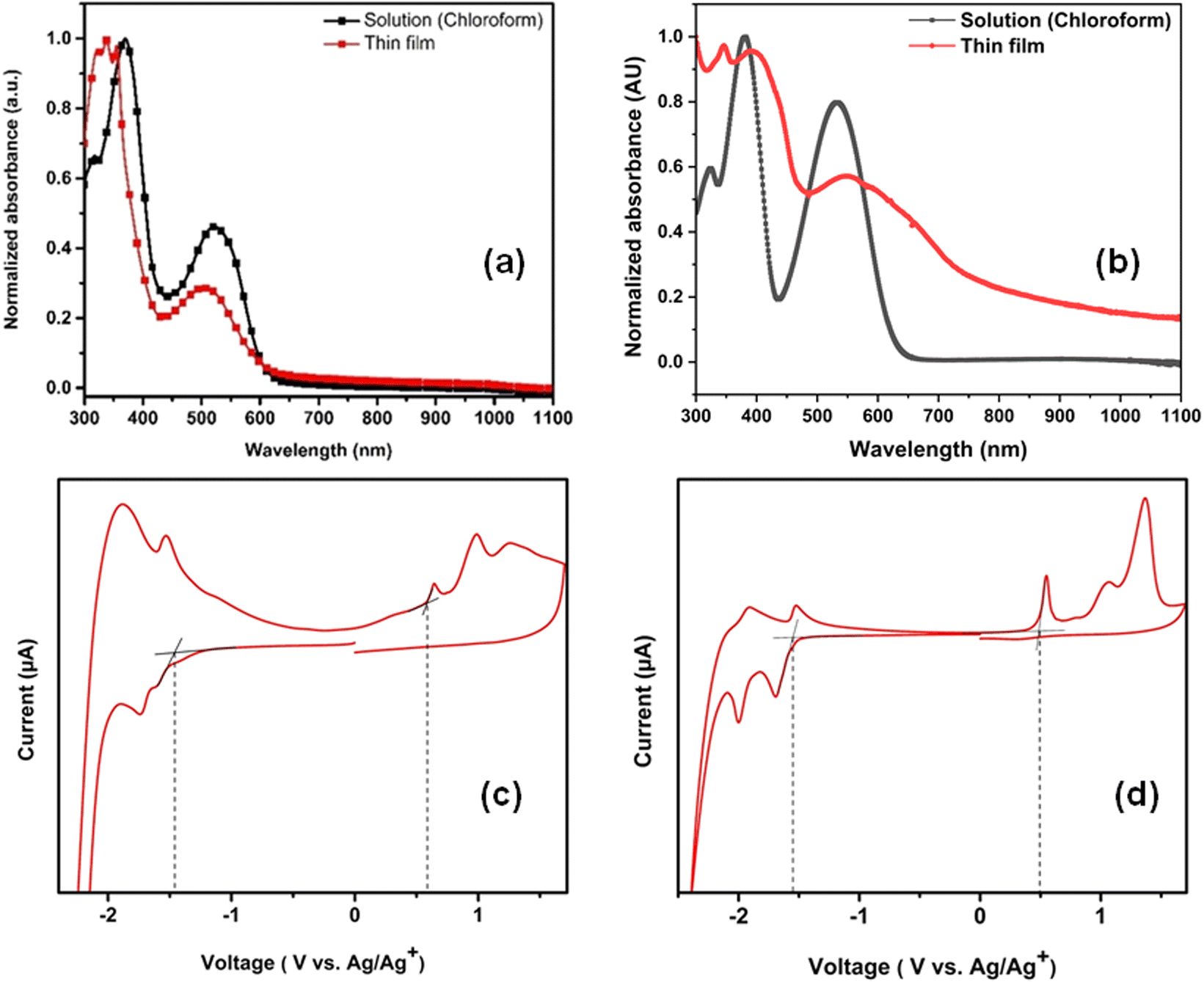 | ||
| Fig. 3 UV-Vis spectra of (a) IN-BT2F-IN and (b) IN-BT2Se-IN. Cyclic voltammograms of (c) IN-BT2F-IN and (d) IN-BT2Se-IN. | ||
Cyclic voltammetry (CV) experiments were performed in the solid state to determine the HOMO and LUMO energy levels and the electrochemical bandgap (Eecg) of IN-BT2F-IN and IN-BT2Se-IN. Fig. 3(c) and (d) present the corresponding cyclic voltammograms. The LUMO and HOMO energy levels were calculated from the onset of the reduction and oxidation peaks of the obtained voltammograms, respectively, using the following equations:
| EHOMO = −(Eox + 4.4) eV and ELUMO = −(Ered + 4.4) eV |
| Small molecule | HOMO (eV) | LUMO (eV) | Eecg (eV) | Eoptg (eV) | λsolmax (nm) | λfilmmax (nm) | λonset (nm) | Work |
|---|---|---|---|---|---|---|---|---|
| IN-BT2F-IN | −4.98 | −2.94 | 2.04 | 2.03 | 369, 521 | 337, 499 | 609 | This work |
| IN-BT2Se-IN | −4.89 | −3.28 | 1.61 | 1.57 | 380, 533 | 404, 560 | 771 | This work |
| IN-BT2T-IN | −4.83 | −2.86 | 1.97 | 1.97 | 369, 510 | 379, 525 | 629 | Reported50 |
When the optoelectronic properties of these molecules were compared with those of the previously reported IN-BT2T-IN, moderate differences were observed. Notably, IN-BT2T-IN also exhibited a redshift when transitioning from solution to thin films, attributed to enhanced intermolecular interactions in the solid state. However, the overall redshift for IN-BT2T-IN was only 15 nm, approximately half of that observed for IN-BT2Se-IN. While selenophene- and thiophene-based derivatives exhibited similar HOMO energy levels, with a slight variation of 0.06 eV, the LUMO energy level was significantly lowered (∼0.42 eV) upon introducing the selenophene moiety. This trend where the LUMO level decreases while the HOMO level remains relatively unchanged due to the incorporation of selenophene units has been reported in the literature for some studies.39,54,55 The incorporation of selenophene in this study further resulted in a reduced energy bandgap compared to thiophene derivatives, reinforcing its influence on optoelectronic properties.
Differential scanning calorimetry (DSC) and thermogravimetric analysis (TGA) was used to study the thermal stability and phase transition behavior of IN-BT2F-IN and IN-BT2Se-IN. TGA was conducted under a nitrogen atmosphere to determine the thermal degradation temperatures of the synthesized molecules. Both IN-BT2F-IN and IN-BT2Se-IN exhibited thermal stability up to ∼350 °C, beyond which rapid degradation occurred. The degradation temperatures (Td), defined by the temperature at which 5% weight loss was observed,26,56 were 288.1 °C for IN-BT2F-IN and 295.3 °C for IN-BT2Se-IN (Fig. S11, ESI†). These results indicate that both molecules possess sufficient thermal stability for thermal treatment processes without significant degradation. Given their high Td values (above 250 °C), DSC analysis was further performed to investigate their thermal transition behaviors. The corresponding DSC thermograms are shown in Fig. S11 (ESI†). IN-BT2F-IN exhibited a melting point (Tm) of 129.9 °C, but no crystallization temperature (Tc) was detected. In contrast, IN-BT2Se-IN displayed a Tm at 138.1 °C and a Tc at 94.6 °C. The higher Tm of IN-BT2Se-IN was attributed to the presence of the heavier selenium atom, which enhances intermolecular interactions compared to oxygen in IN-BT2F-IN, contributing to its greater thermal stability.
OFET characteristics were examined using a bottom-gate-bottom-contact (BGBC) device configuration, as shown in Fig. 4. Both small molecules were tested under ambient conditions after being fabricated on an OTMS-treated SiO2/n++-Si substrate. IN-BT2Se-IN exhibited OFET activity in non-annealed thin films, which improved upon thermal annealing. The charge carrier mobility, threshold voltage (VT), and the on/off current ratio (Ion/Ioff) are the important factors that determine the switching efficiency, stability, overall reliability, and the performance of OFET devices. The average hole mobility of the devices was slightly enhanced by a factor of ∼4 through annealing at 80 °C, below the crystallization temperature. However, annealing at 100 °C, slightly above its cold crystallization temperature, improved the hole mobility by two orders of magnitude. The maximum hole mobility obtained under optimized conditions was 2.57 × 10⁻² cm2 V−1 s−1, with an average of 1.92 × 10⁻² cm2 V−1 s−1. The maximum hole mobility reported based on the selenophene-based small molecules is 0.463 cm2 V−1 s−1.38 The threshold voltage is the minimum gate voltage required to induce and initiate the charge carrier conduction in the transistor channel region. VT was calculated in the range from 6.7 V to −8.9 V under optimized conditions at 100 °C annealing, with a slightly narrower range than non-annealed devices (12.7 to (−7.1)) and devices annealed at 80 °C (10.5 to (−6.3)). This narrowing in the VT with annealing conditions suggests improvement in the thin film quality and uniform accumulation of charge carriers, resulting in consistent device behavior. The lowest threshold voltage reported for the selenophene-based D–A molecule was ∼−0.4 V under annealing conditions.47 Moreover, the on–off current ratio (Ion/Ioff), which is an important parameter for examining the efficiency of transistor switching, drastically improved from 103 (for both devices, non-annealed and annealed at 80 °C) to 105–106 for optimized devices under annealing conditions at 100 °C, indicating better charge transport properties and reduced leakage currents as a result of improved molecular alignment and material morphology. A higher Ion/Ioff ratio ensures a minimum leakage current (typically resulting from reduced trap densities due to better molecular alignment at annealed temperature) in the off-state, leading to improved signal integrity and power efficiency in electronic devices. Conversely, IN-BT2F-IN exhibited no OFET activity. Devices made from IN-BT2F-IN showed flat-line curves with low current values (∼10−13 to 10−12 A) upon increasing VG at VD = −40 V. In a study, a similar trend with reduced hole mobility was observed when furan was introduced as a bridge in a polymer. This study suggested that the furan incorporation resulted in altered atomic interaction among the adjacent blocks in the polymer backbone, leading to the coplanarity in the polymer becoming worse. The coplanarity eventually influenced less ordered intermolecular packing in thin film as evidenced by X-ray diffraction and atomic force microscopy characterization.57 Similarly, there could be a possibility of having a disordered arrangement of molecules, possibly making the thin film poor, resulting in hindrance of the charge transport, which was further characterized by TM-AFM and GI-XRD. Compared to its thiophene-based analog (IN-BT2T-IN), IN-BT2Se-IN showed an order of magnitude improvement in hole mobility while maintaining similar Ion/Ioff values and operating at lower voltages (VD = −40 V/VG = −40 V) compared to VD = −100 V/VG = −100 V for IN-BT2T-IN.50 OFET parameters obtained from transfer and output curves are summarized in Table 2.
 | ||
| Fig. 4 Transfer (top) and output (bottom) curves of the IN-BT2Se-IN molecule under varying thermal annealing settings, annealed for 1 hour in nitrogen. | ||
| Annealing temperature (°C) | Maximum hole mobility (cm2 V−1 s−1) | Average hole mobilitya (cm2 V−1 s−1) | Threshold voltage (VT) (V) | Ion/off |
|---|---|---|---|---|
| a Derived from the data collected across six devices, and measurements were taken for BGBC devices with dimensions of W = 457 μm and L = 20 μm under an applied VD of −40 V. Under ambient conditions, thin films were deposited at 300 rpm from chloroform solutions with a concentration of 5 mg mL−1, and then thermally annealed in nitrogen for 1 hour. | ||||
| Non-annealed | 3.28 × 10⁻⁴ | 1.56 × 10⁻⁴ | 12.7 to (−7.1) | 103 |
| 80 | 9.30 × 10⁻⁴ | 6.50 × 10⁻⁴ | 10.5 to (−6.3) | 103 |
| 100 | 2.57 × 10⁻² | 1.92 × 10⁻² | 6.7 to (−8.9) | 105–106 |
Tapping-mode atomic force microscopy (TMAFM) was used to investigate the surface morphology of fabricated thin-film devices. TMAFM analysis was conducted on non-annealed and annealed (100 °C) thin films in the channel region of OFET devices with the best-reported hole mobilities. TMAFM analysis provided insight into surface topology and root mean square roughness (RMS) values. Height and phase images at the corresponding annealing temperatures are shown in Fig. 5.
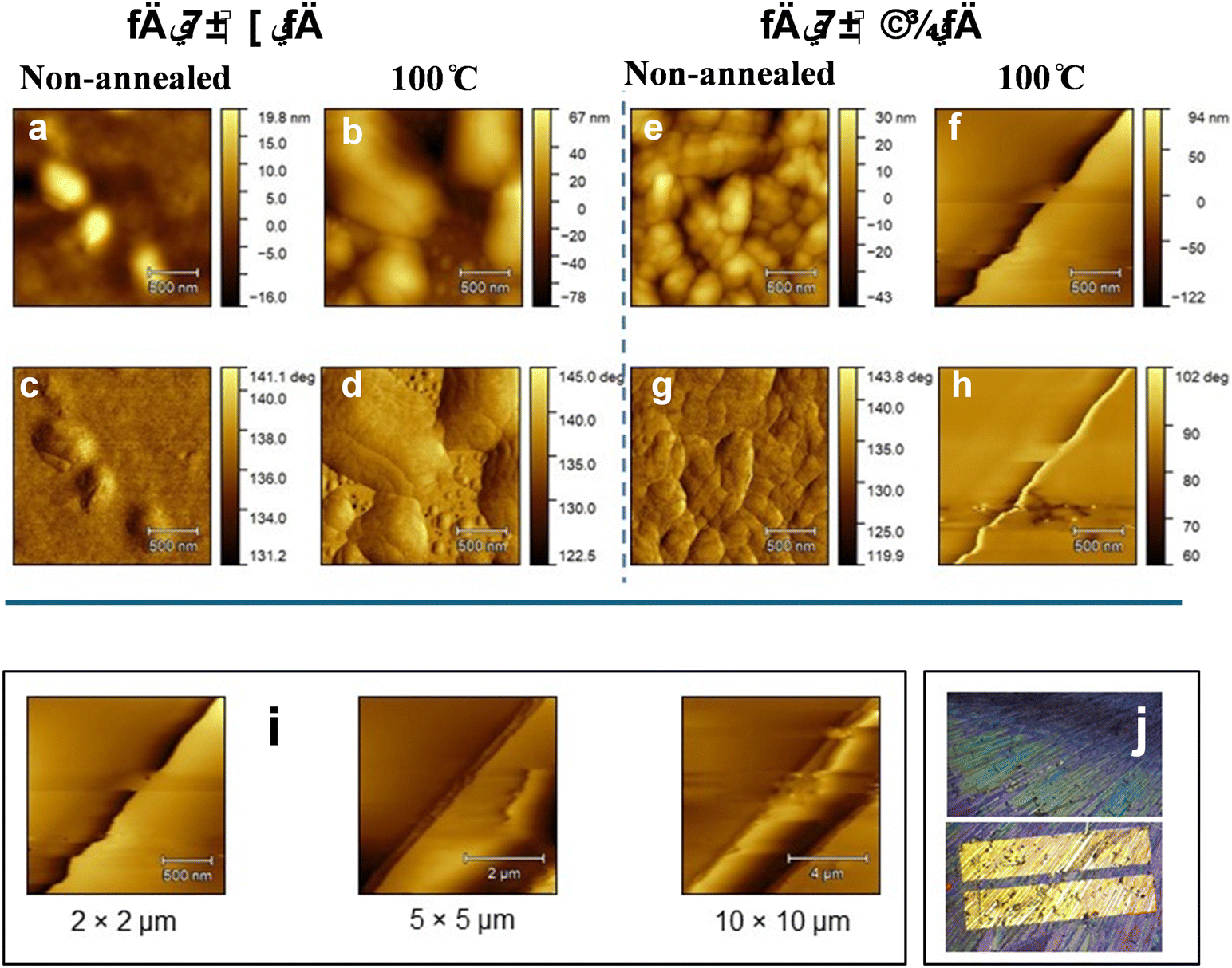 | ||
| Fig. 5 (a) TMAFM images illustrating the height (top) and phase (bottom) data for IN-BT2F-IN (left half) and IN-BT2Se-IN (right half); the first column (a), (c), (e) and (g) includes non-annealed films images, while annealed films at 100 °C images are shown in the second column (b), (d), (f) and (h). (i) TMAFM height images scanned for IN-BT2Se-IN annealed films (100 °C) using varying window sizes (2 × 2 μm, 5 × 5 μm, and 10 × 10 μm, left to right) to highlight morphological features. (j) TMAFM's focusing camera images show thin films fabricated on transistor devices: OTMS-modified silica (top) and gold electrodes with channel regions (bottom). | ||
For IN-BT2F-IN, non-annealed thin films showed no distinct topological features except for minor bubble-like artifacts on the surface, likely caused by trapped air between the silicon substrate and the thin film (Fig. 5). After annealing at 100 °C, no significant improvement was observed in crystalline features, but the trapped air seemed to have a widely spread bubble-like form by the expansion of small bubbles in the scanned area. Consequently, the RMS roughness increased from 5.54 nm to 27.60 nm upon annealing. In contrast, the non-annealed thin films of IN-BT2Se-IN revealed small crystalline domains, further expanding into relatively larger, elongated plate-like domains after thermal annealing at 100 °C. Here, the RMS roughness increased from 10.60 nm to 32.70 nm compared to non-annealed films. Expanded-area scanning was conducted to explore further the long-range ordered plate-like features on the thin-film surface, as shown in Fig. 5b. This confirmed the presence of long-range dispersed crystalline boundaries. As the scanned area increased, the calculated RMS values increased from 31.79 nm to 62.82 nm to 78.30 nm (Fig. 5i). Additionally, the TMAFM focusing camera image is provided in Fig. 5j, which shows the thin films fabricated on transistor devices over OTMS-modified silica and the gold electrodes with channel regions, respectively, further demonstrating how the thermally annealed thin film displayed its crystalline topographies. IN-BT2Se-IN exhibited better crystalline thin-film morphology under optimized conditions than the previously reported thiophene derivative. These morphological changes observed in TM-AFM upon annealing thin films of IN-BT2Se-IN result in improvement in the crystalline feature, eventually responsible for better VT, Ion/Ioff ratio, and hole mobility. These results align well with the mobility data trends for these small molecules.
Out-of-plane grazing incidence X-ray diffraction (GIXRD) analysis was accomplished on both non-annealed and annealed (100 °C) thin films to investigate the crystallinity of these small molecules further. The obtained GIXRD spectra for both small molecules are shown in Fig. 6. For IN-BT2F-IN, the GIXRD spectra of both annealed and non-annealed thin films displayed no distinctive intense diffraction peaks that indicate a lack of a significant degree of crystallinity. This data further confirmed that the surface features observed in TMAFM images of both annealed and non-annealed thin films of the molecule IN-BT2F-IN were not crystalline. This non-crystalline behavior of the thin film indicates the possible random orientation of the molecules, which affects the intermolecular packing order, resulting in poor thin film forming ability, as supported by the AFM studies. However, in the case of IN-BT2Se-IN, the thin film annealed at 100 °C exhibited a highly intense and narrower diffraction peak, arising from the first order (100) crystalline plane, indicating long-range ordered crystalline domains in the thin film. In the annealed thin film of IN-BT2Se-IN, a (100) Bragg's reflection peak was observed at 2θ = 3.45°, corresponding to a lamellar d-spacing of 25.6 Å. This indicates the presence of well-ordered edge-on-oriented molecules, likely influenced by the OTMS-treated silicon dioxide surface. The molecule IN-BT2Se-IN exhibited a comparable lamellar d-spacing value (25.9 Å for IN-BT2T-IN) but with ∼10 times greater intensity in the (100) peak, demonstrating the better crystalline nature of IN-BT2Se-IN when compared to the previously reported IN-BT2T-IN. This result strongly correlates with the enhanced hole mobility observed for IN-BT2Se-IN, explaining the improved OFET performance.
 | ||
| Fig. 6 Grazing incidence X-ray diffraction patterns of (a) IN-BT2F-IN and (b) IN-BT2Se-IN. | ||
Conclusions
In summary, two D–A–D small molecules based on indole (donor) and benzothiadiazole (acceptor), incorporating selenophene and furan spacers, were synthesized and their optoelectronic and thin-film properties were evaluated, followed by their application in OFET devices. The findings were evaluated alongside previously reported thiophene analogs to analyze the impact of changing the chalcogenophene spacer on the structure–property correlation in indole- and BT-based D–A–D small molecules. Optoelectronic studies suggested that the incorporation of selenophene into the molecular design (IN-BT2Se-IN) significantly reduced the energy bandgap by lowering the LUMO level by approximately 0.4 eV compared to the thiophene derivative (IN-BT2T-IN). In contrast, both thiophene and furan derivatives exhibited an almost identical energy bandgap, but the thiophene analog had relatively higher HOMO and LUMO energy levels. OFET data for IN-BT2Se-IN displayed an average hole mobility of 1.92 × 10⁻² cm2 V−1 s−1, with a maximum of 2.57 × 10⁻² cm2 V−1 s−1. At the same time, IN-BT2F-IN showed no OFET activity due to the random orientation of the molecules, which led to the non-crystalline thin film formation. Compared to IN-BT2T-IN, IN-BT2Se-IN demonstrated hole mobility that was one order of magnitude greater, along with operation at lower voltages under similar thermal treatment and device architectures.50 The results of TMAFM experiments strongly indicated that IN-BT2Se-IN has a highly ordered thin-film morphology superior to that of its furan derivative. Compared to the thiophene derivatives reported earlier, IN-BT2Se-IN exhibited long-range crystalline domains validated by topological height data and RMS values. GIXRD analysis provided additional evidence for forming these highly ordered thin films. In conclusion, experimental results from optoelectronic, morphological, and GIXRD studies strongly supported the observed mobility trends. This study highlights the impact of spacer unit variations in the molecular backbone on optoelectronic properties and their correlation with forming long-range order crystalline domains in thin-film devices. This strategy is beneficial for designing and developing new organic small molecules with controlled optoelectronic properties for various electronic applications.Conflicts of interest
There are no conflicts to declare.Data availability
The data supporting this article have been included as part of the ESI,† which contains additional detailed experimental procedures, NMR spectra, MALDI-TOF data, DSC, and TGA thermograms.Acknowledgements
M. C. S. thanks the Eugene McDermott Foundation for generous endowed chair support.References
- H. Sirringhaus, Adv. Mater., 2014, 26, 1319–1335 CrossRef CAS PubMed
.
- A. C. Arias, J. D. MacKenzie, I. McCulloch, J. Rivnay and A. Salleo, Chem. Rev., 2010, 110, 3–24 CrossRef CAS PubMed
- C. Winder and N. S. Sariciftci, J. Mater. Chem., 2004, 14, 1077–1086 RSC
- M. Muccini, Nat. Mater., 2006, 5, 605–613 CrossRef CAS PubMed
- S. Allard, M. Forster, B. Souharce, H. Thiem and U. Scherf, Angew. Chem., Int. Ed., 2008, 47, 4070–4098 CrossRef CAS PubMed
- J. Takeya, M. Yamagishi, Y. Tominari, R. Hirahara, Y. Nakazawa, T. Nishikawa, T. Kawase, T. Shimoda and S. Ogawa, Appl. Phys. Lett., 2007, 90, 102120 CrossRef
- J. Mei, Y. Diao, A. L. Appleton, L. Fang and Z. Bao, J. Am. Chem. Soc., 2013, 135, 6724–6746 CrossRef CAS PubMed
- M. A. Reyes-Martinez, A. J. Crosby and A. L. Briseno, Nat. Commun., 2015, 6, 6948 CrossRef CAS PubMed
- M. D. Yi, J. L. Guo, W. Li, L. H. Xie, Q. L. Fan and W. Huang, RSC Adv., 2015, 5, 95273–95279 RSC
- L. Han, P. Mandlik, K. H. Cherenack and S. Wagner, Appl. Phys. Lett., 2009, 94, 162105 CrossRef
- K. Pangal, J. C. Sturm, S. Wagner and N. Yao, IEEE Trans. Electron Devices, 2000, 47, 1599–1607 CrossRef CAS
- T. Meguro and A. Hara, IEICE Trans. Electron., 2017, E100c, 94–100 CrossRef
- O. D. Jurchescu, J. Baas and T. T. M. Palstra, Appl. Phys. Lett., 2004, 84, 3061–3063 CrossRef CAS
- J. E. Anthony, J. Gierschner, C. A. Landis, S. R. Parkin, J. B. Sherman and R. C. Bakus Ii, Chem. Commun., 2007, 4746–4748, 10.1039/b711296c
- H. Li, G. Giri, J. B.-H. Tok and Z. Bao, MRS Bull., 2013, 38, 34–42 CrossRef CAS
- R. Bhatia, D. Wadhawa, G. Gurtu, J. Gaur and D. Gupta, J. Saudi Chem. Soc., 2019, 23, 925–937 CrossRef CAS
- A. Afzali, C. D. Dimitrakopoulos and T. L. Breen, J. Am. Chem. Soc., 2002, 124, 8812–8813 CrossRef CAS PubMed
- H. Meng, J. Zheng, A. J. Lovinger, B. C. Wang, P. G. Van Patten and Z. N. Bao, Chem. Mater., 2003, 15, 1778–1787 CrossRef CAS
- M. J. Kang, I. Doi, H. Mori, E. Miyazaki, K. Takimiya, M. Ikeda and H. Kuwabara, Adv. Mater., 2011, 23, 1222–1225 CrossRef CAS PubMed
- C. D. Dimitrakopoulos and P. R. L. Malenfant, Adv. Mater., 2002, 14, 99 CrossRef CAS
- Y. Li, S. P. Singh and P. Sonar, Adv. Mater., 2010, 22, 4862–4866 CrossRef CAS PubMed
- W. Li, K. H. Hendriks, W. S. Roelofs, Y. Kim, M. M. Wienk and R. A. Janssen, Adv. Mater., 2013, 25, 3182–3186 CrossRef CAS PubMed
- R. Søndergaard, M. Hösel, D. Angmo, T. T. Larsen-Olsen and F. C. Krebs, Materials
Today, 2012, 15, 36–49 CrossRef
- B. Lim, H. Sun, J. Lee and Y. Y. Noh, Sci. Rep., 2017, 7, 164 CrossRef PubMed
- C. Bulumulla, R. Gunawardhana, R. N. Kularatne, M. E. Hill, G. T. McCandless, M. C. Biewer and M. C. Stefan, ACS Appl. Mater. Interfaces, 2018, 10, 11818–11825 CrossRef CAS PubMed
- Z. Ma, C. M. Udamulle Gedara, H. Wang, M. C. Biewer and M. C. Stefan, ACS Appl. Mater. Interfaces, 2023, 15, 46119–46129 CrossRef CAS PubMed
- P. L. Gamage, C. M. Udamulle Gedara, R. Gunawardhana, C. Bulumulla, Z. Ma, A. Shrivastava, M. C. Biewer and M. C. Stefan, Appl. Sci., 2022, 12, 3150 CrossRef CAS
- C. M. Udamulle Gedara, Z. Ma, M. M. Talukder, R. Gunawardhana, M. C. Biewer and M. C. Stefan, ACS Appl. Electron. Mater., 2022, 4, 5340–5350 CrossRef CAS
- C. Bulumulla, R. Gunawardhana, S. H. Yoo, C. R. Mills, R. N. Kularatne, T. N. Jackson, M. C. Biewer, E. D. Gomez and M. C. Stefan, J. Mater. Chem. C, 2018, 6, 10050–10058 RSC
- I. Kang, T. K. An, J. A. Hong, H. J. Yun, R. Kim, D. S. Chung, C. E. Park, Y. H. Kim and S. K. Kwon, Adv. Mater., 2013, 25, 524–528 CrossRef CAS PubMed
- A. J. Kronemeijer, E. Gili, M. Shahid, J. Rivnay, A. Salleo, M. Heeney and H. Sirringhaus, Adv. Mater., 2012, 24, 1558–1565 CrossRef CAS PubMed
- A. Patra and M. Bendikov, J. Mater. Chem., 2010, 20, 422–433 RSC
- J. Hollinger, A. A. Jahnke, N. Coombs and D. S. Seferos, J. Am. Chem. Soc., 2010, 132, 8546–8547 CrossRef CAS PubMed
- D. Gao, J. Hollinger and D. S. Seferos, ACS Nano, 2012, 6, 7114–7121 CrossRef CAS PubMed
- Q. Liu, Y. Wang, A. Kohara, H. Matsumoto, S. Manzhos, K. Feron, S. E. Bottle, J. Bell, T. Michinobu and P. Sonar, Adv. Funct. Mater., 2020, 30, 1907452 CrossRef CAS
- Q. Liu, W. He, Y. Shi, S. Otep, W. L. Tan, S. Manzhos, C. R. McNeill, X. Guo, P. Sonar and T. Michinobu, Chem. Mater., 2022, 34, 3140–3151 CrossRef CAS
- P. L. Gamage, C. M. Udamulle Gedara, Z. Ma, A. Bhadran, R. Gunawardhana, C. Bulumulla, M. C. Biewer and M. C. Stefan, ACS Appl. Electron. Mater., 2021, 3, 5335–5344 CrossRef CAS
- A. Velusamy, Y. Y. Chen, M. H. Lin, S. N. Afraj, J. H. Liu, M. C. Chen and C. L. Liu, Adv. Sci., 2024, 11, 2305361 CrossRef CAS PubMed
- H. Y. Chen, S. C. Yeh, C. T. Chen and C. T. Chen, J. Mater. Chem., 2012, 22, 21549–21559 RSC
- F.-Y. Cao, C.-C. Tseng, F.-Y. Lin, Y. Chen, H. Yan and Y.-J. Cheng, Chem. Mater., 2017, 29, 10045–10052 CrossRef CAS
- P. T. Yu, G. T. Feng, J. Y. Li, C. Li, Y. H. Xu, C. Y. Xiao and W. W. Li, J. Mater. Chem. C, 2020, 8, 2790–2797 RSC
- S. Ye, V. Lotocki, H. Xu and D. S. Seferos, Chem. Soc. Rev., 2022, 51, 6442–6474 RSC
- Y. Zuo, Q. Zhang, X. J. Wan, M. M. Li, H. J. Zhang, C. X. Li and Y. S. Chen, Org. Electron., 2015, 19, 98–104 CrossRef CAS
- W. Gao, Q. S. An, R. J. Ming, D. J. Xie, K. L. Wu, Z. H. Luo, Y. Zou, F. J. Zhang and C. L. Yang, Adv. Funct. Mater., 2017, 27, 1702194 CrossRef
- Y. Shin, C. E. Song, W. H. Lee, S. K. Lee, W. S. Shin and I. N. Kang, Macromol. Rapid Commun., 2017, 38, 1700016 CrossRef PubMed
- A. V. Marsh and M. Heeney, Polym. J., 2023, 55, 375–385 CrossRef CAS
- J. G. Oh, Y. H. Ha, J.-H. Kim, S.-K. Kwon, T. K. An, Y.-H. Kim and J. Jang, Org. Electron., 2021, 89, 106032 CrossRef CAS
- P. Sonar, S. P. Singh, P. Leclère, M. Surin, R. Lazzaroni, T. T. Lin, A. Dodabalapur and A. Sellinger, J. Mater. Chem., 2009, 19, 3228–3237 RSC
- J. Du, M. C. Biewer and M. C. Stefan, J. Mater. Chem. A, 2016, 4, 15771–15787 RSC
- C. M. Udamulle Gedara, A. Shrivastava, Z. Ma, P. L. Gamage, C. Bulumulla, D. S. Dissanayake, M. M. Talukder, M. C. Stefan and M. C. Biewer, ACS Omega, 2025, 10, 12357–12365 CrossRef CAS PubMed
- Y.-J. Hwang, N. M. Murari and S. A. Jenekhe, Polym. Chem., 2013, 4, 3187–3195 RSC
- A. Patra, M. Bendikov and S. Chand, Acc. Chem. Res., 2014, 47, 1465–1474 CrossRef CAS PubMed
- F. Qi, F. R. Lin and A. K. Y. Jen, Solar RRL, 2022, 6, 2200156 CrossRef CAS
- Q. Liu, S. Kumagai, S. Manzhos, Y. Q. Chen, I. Angunawela, M. M. Nahid, K. Feron, S. E. Bottle, J. Bell, H. Ade, J. Takeya and P. Sonar, Adv. Funct. Mater., 2020, 30, 2000489 CrossRef CAS
- B. Kim, H. R. Yeom, M. H. Yun, J. Y. Kim and C. Yang, Macromolecules, 2012, 45, 8658–8664 CrossRef CAS
- S. Oh, H. Kang, C. Kim and S. Seo, J. Mater. Chem. C, 2025, 13, 12675–12684 RSC
- J. Yuan, Y. Zang, H. Dong, G. Liu, C.-A. Di, Y. Li and W. Ma, Polym. Chem., 2013, 4, 4199–4206 RSC
Footnotes |
| † Electronic supplementary information (ESI) available: Additional detailed experimental procedure and NMR, MALDI-TOF, DSC, and TGA results. See DOI: https://doi.org/10.1039/d5tc01678a |
| ‡ C. M. U. G. and A. S. contributed equally and should be considered co-first authors. |
| This journal is © The Royal Society of Chemistry 2025 |