
Ab initio quantum transport simulation of the sub-1 nm gate-length monolayer and bilayer α-MoTe2 field-effect transistors
Mudasser Husain a,
Younas Ahmeda,
Xingyue Yanga,
Shibo Fangg,
Zongmeng Yanga,
Jichao Donga,
Linqiang Xua,
Nasir Rahmanb and
Jing Lu*acdef
a,
Younas Ahmeda,
Xingyue Yanga,
Shibo Fangg,
Zongmeng Yanga,
Jichao Donga,
Linqiang Xua,
Nasir Rahmanb and
Jing Lu*acdef
aState Key Laboratory for Mesoscopic Physics and Department of Physics, Peking University, Beijing 100871, P. R. China. E-mail: jinglu@pku.edu.cn
bDepartment of Physics, University of Lakki Marwat, Lakki Marwat, KPK, Pakistan
cCollaborative Innovation Center of Quantum Matter, Beijing 100871, P. R. China
dBeijing Key Laboratory for Magnetoelectric Materials and Devices, Beijing 100871, P. R. China
eBeijing Key Laboratory for Magnetoelectric Materials and Devices (BKL-MEMD), Peking University, Beijing 100871, P. R. China
fPeking University Yangtze Delta Institute of Optoelectronics, Nantong 226010, P. R. China
gScience, Mathematics and Technology (SMT) Cluster, Singapore University of Technology and Design, 487372, Singapore
First published on 30th June 2025
Abstract
Two-dimensional semiconducting α-MoTe2 is a promising channel material for the field-effect transistors (FETs). Recently, the performance limit of the sub-5 nm gate-length n- and p-type monolayer and multilayer α-MoTe2 transistors has been reported theoretically. However, this material is still unexplored for the ultra-short (sub-1 nm) gate-length n- and p-type metal–oxide semiconductor field-effect transistors (MOSFETs). Here, we performed ab initio quantum transport simulation of the 0.34 nm gate-length n- and p-type MOSFET based on the monolayer (ML) and bilayer (BL) α-MoTe2 for high-performance (HP) and low-power (LP) applications. The proposed n-type ML α-MoTe2 transistor achieves an on-state current (Ion) of 396 μA μm−1 for HP and 183 μA μm−1 for LP, and intrinsic delay time (τ) of 0.334 ps for HP and 1.075 ps for LP. It also exhibits a power delay product (PDP) of 0.071 fJ μm−1 for HP and 0.060 fJ μm−1 for LP, thereby satisfying the International Technology Roadmap for Semiconductors (ITRS) requirements for both HP and LP applications. Unfortunately, the p-type ML and the n and p-type BL α-MoTe2 transistors fail to achieve the required Ion to meet the ITRS standard for HP and LP applications. This research extends the potential application of the ML α-MoTe2 from the sub-5 nm gate-length FETs to the sub-1 nm region.
1. Introduction
Transistor technology has played a pivotal role in advancing modern electronics.1 The crucial driving force behind the advancement and miniaturization of modern electronics adheres to the scaling principle of Moore's law.2 Moore's law predicted that the number of transistors per square centimeter in integrated circuits (ICs) doubles every two years, which increases computing power and lowers cost. Since the invention of the first point-contact transistor in 1947, transistor technology has continuously evolved, leading to the development of silicon-based Fin field-effect transistors (FinFETs) designed to address the need for smaller, faster, and more energy-efficient devices.3,4 The mainstream Si-FinFETs show improved device performance relative to conventional planar transistors.5 However, as the gate-length approaches 10-nm, the Si-FinFETs suffer from short-channel effects (SCEs), which reduce gate controllability.4 This results in increased leakage currents, leading to higher power consumption. Additionally, the limited carrier mobility of Si due to the intrinsic scaling limits restricts switching speeds, thereby hindering the overall performance of the ultra-scaled Si-transistors. Incorporating new structure transistors, alternative channel materials, or new principle transistors is imperative to overcome these challenges and sustain Moore's law life.6–82D semiconductors, notably TMDCs, have emerged as promising alternative channel materials for the ultra-scaled MOSFETs, playing a crucial role in advancing next-generation electronic devices.9,10 The atomic-layer thickness of the TMDC materials provides exceptional electrostatic control and effectively mitigates SCEs. In TMDCs, the smooth surfaces and absence of out-of-plane dangling bonds lead to high carrier mobility, thereby enhancing the performance of the device.11 Furthermore, the atomic-layer stacking-dependent tunable band gap of 2D materials enables the development of more energy-efficient transistors tailored to advanced technology nodes.12,13 In TMDCs, the MoTe2 exists in two stable phases, semiconducting 2H and semimetallic 1T′. There is a minimal energy difference (typically <0.1 eV per atom) between its 2H and 1T′ phases, enabling reversible and controllable phase transitions crucial for phase-engineered nanoelectronic devices.14 The semiconducting α-MoTe2 featuring a moderate band gap of 1.1 eV in the ML, similar to silicon (1.1 eV), stands out as a promising channel material for field-effect transistors. The moderate bandgap is more suitable for low-voltage operation and high on-state current, striking a balance between sufficient carrier injection of either electrons for n-FETs or holes for p-FETs. This balance underscores the unique potential of MoTe2 as a channel material for ultra-scaled transistor technologies compared to other 2D TMDCs. MoTe2 exhibits highly ambipolar and tunable polarity-controllable transport, attributed to its more symmetric band alignment and reduced Schottky barrier heights for both electrons and holes. This tunability makes MoTe2 particularly promising for reconfigurable and complementary logic devices, where both n-type and p-type transistors can be realized by selecting appropriate metal contacts.
In transistors, scaling down the gate-length (Lg) has been a key focus for researchers aiming to push the limits of device miniaturization.7,15,16 In 2022, Fan Wu et al.17 fabricated side-wall MoS2 transistors using a single graphene-layer-edge as the gate electrode, achieving an ultra-short physical gate length of 0.34 nm. These devices exhibited subthreshold swing (SS) values as low as 117 mV dec−1 and a current on/off ratio (Ion/Ioff) of up to 1.02 × 10⁵, highlighting the potential for continued scaling of transistors following Moore's law. However, despite the aggressive gate downscaling, these transistors suffer from limited Ion, primarily due to a relatively long channel, thick gate dielectric, and Schottky barriers at the metal-semiconductor interface. In addition to experiments, ab initio quantum simulations of the double-gated n- and p-type ML MoS2 transistors featuring a gate-length of 0.34 nm have been reported in 2024 by Ying Li et al.,18 demonstrating superior performance to the 1-nm gate-length ML MoS2 transistors. In 2025, Xingyue Yang et al.19 reported the ML and BL WSe2 p-FETs with a gate-length of 0.34 nm, utilizing ab initio quantum transport simulations to assess their performance. The ML WSe2 p-FETs, with a channel length of less than 5 nm, achieve a high Ion of 712 μA μm−1, in line with the ITRS standard requirement for HP devices. In contrast, the BL WSe2 p-FETs show a 40% reduction in Ion, attributed to changes in the band structure and degradation of gate control. Theoretical and experimental research on the sub-1 nm Lg transistors based on other 2D TMDC materials is also highly anticipated.
Many researchers reported the n- and p-type transistors based on the ML and multilayer α-MoTe2 for HP and LP devices.20–22 Notably, Qi Zhang et al. have demonstrated state-of-the-art 1T′-2H heterophase bilayer MoTe2 FETs with a gate length of 4 nm, achieving excellent switching behavior, including a subthreshold swing of ∼73 mV decade−1 and an on/off current ratio of ∼105.23 Qiang Li et al.24 recently used ab initio quantum transport simulations to evaluate the ultimate performance of the ML α-MoTe2 n- and p-type transistors down to 1-nm gate-length for HP and LP device applications. They found that the Ion of the 3-nm gate-length p-type ML α-MoTe2 transistor meets the ITRS standard for both HP and LP applications. Although 2D α-MoTe2 is regarded as a promising alternative channel material for the n- and p-type FETs down to 1-nm gate-length, this material remains unexplored for the sub-1 nm gate-length transistors. It remains a topic of research interest in terms of three challenges. (1) What is the fundamental scaling limit of the ML and BL α-MoTe2 FETs? (2) Does the ultimate performance of the ML and BL α-MoTe2 FETs meet the ITRS requirements? (3) Does the ML and BL α-MoTe2 exhibit superior performance to the most studied ML MoS2 for FETs with sub-1 nm gate-length scale?
In this research, we aim to address these three challenges by performing ab initio quantum transport simulation of the n- and p-type MOSFET with the 0.34 nm gate-length based on the ML and BL α-MoTe2 for HP and LP applications operating at an ultra-low supply voltage (Vdd) of 0.54 V. The 0.34 nm gate-length n-type transistor based on the ML α-MoTe2 with a 2-nm underlap meets the ITRS standards for HP and LP applications. For the BL α-MoTe2 transistor, we find that BL α-MoTe2 exhibits an indirect band gap due to interlayer coupling, leading to a flatter valence band and higher hole effective mass. This reduced band dispersion significantly limits carrier mobility, particularly for holes, thereby degrading the on-state current and overall device performance. These changes explain why BL α-MoTe2 MOSFET configurations in particular fail to meet the ITRS standard for HP and LP applications. Therefore, the performance of the n-type ML α-MoTe2 transistor is evaluated by calculating key figures-of-merit (FOMs) following the ITRS guidelines. The key FOMs include SS, transconductance, power delay product (PDP), and intrinsic delay-time (τ). This study explores the potential of ML α-MoTe2 as a 2D nanochannel material for next-generation ultra-scaled FETs.
2. Device model and simulation methodology
We considered the two-probe and double-gated FET device model for the quantum transport simulations. A two-probe model comprises a central channel region attached to the two bulk electrodes, i.e., the left electrode (source) and the right electrode (drain).25 The central channel region of the device usually characterizes the material under investigation. The left and right electrodes work as electrical terminals through which electrical signals are applied. Fig. 1 shows the configuration of our two-probe and double-gated device, in which the pristine 2D semiconducting ML/BL α-MoTe2 are considered as the channel material. The electrode regions are heavily n- or p-type doped ML/BL α-MoTe2 and act as source and drain terminals at the left and right portions. The source and drain electrodes are assumed to have bulk properties. Two metallic gates (top and bottom) of the 0.34 nm Lg are applied and separated from the channel region using the high-k HfO2 as a gate-dielectric material. The effective oxide thickness (EOT) is maintained at 0.26 nm, as specified by the ITRS guidelines.26,27 It is well known that in addition to EOT, the physical oxide thickness (TOX) also plays a critical role in controlling short-channel effects (SCEs). The physical thickness of the oxide layer varies with the dielectric constant (k) to maintain a fixed EOT, as described by the relationship:28 . For HfO2, with a dielectric constant kOX ≈ 25, and SiO2 having kSiO2 = 3.9, the resulting physical thickness TOX of 1.66-nm is adjusted accordingly in the simulation. The underlap length (UL) refers to the physical distance between the edge of the gate electrode and the beginning of the source or drain region. A symmetrical UL is considered on both sides of the channel to realize uniform electrostatic control, mitigate SCEs, and enhance overall device performance.29 In the quantum transport simulation of the device, the three spatial regions, i.e., source, drain, and channel, have Neumann and periodic boundary conditions along the x and y directions, respectively. In the transport z-direction, the source and drain regions act as equilibrium bulk materials having periodic boundary conditions, while in the channel region, the Dirichlet boundary conditions are considered.30 A Dirichlet boundary condition is applied at the metallic gate electrode to set a defined potential. In contrast, Neumann boundary conditions are used in the dielectric region to represent electrically insulating boundaries.
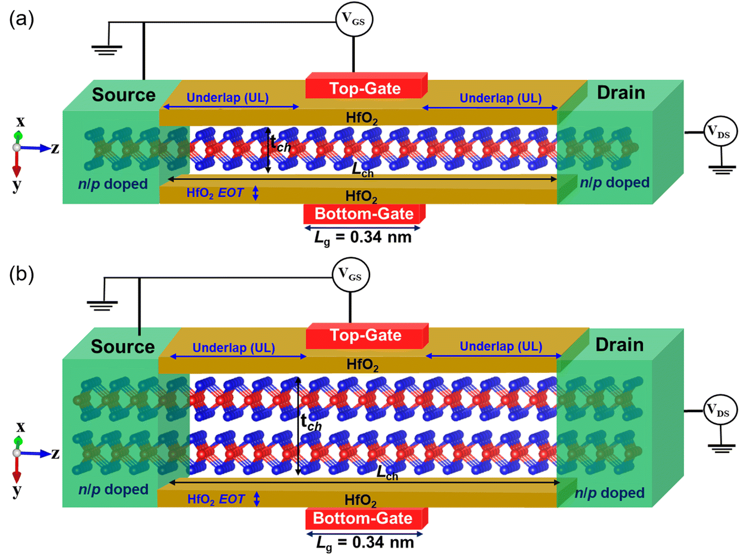 | ||
| Fig. 1 Two-probe and double-gated device models featuring the 0.34-nm Lg (a) ML and (b) BL α-MoTe2 FETs. | ||
The transport properties of the 0.34-nm Lg ML/BL α-MoTe2 transistors are analyzed using the DFT + NEGF formalism31,32 implemented within the advanced atomic-scale quantum Atomistix ToolKit (ATK) simulation package.30 The ML and BL (AB-stacking) of the α-MoTe2 are first optimized by considering a vacuum spacing of 20 Å along the out-of-plane direction to avoid artificial interactions of the period images. In geometry optimization, the limited memory Broyden–Fletcher–Goldfarb–Shanno (LBFGS) method is employed to relax the ML and BL α-MoTe2. The calculations are considered fully converged when the force is below 0.01 eV Å−1 and the stress error tolerance is within 0.001 eV Å−3, ensuring accurate and reliable results. A basis set of linear combinations of atomic orbitals (LCAO) with a density-mesh cutoff of 125 Hartree is regarded for our DFT calculations. To fully estimate the exchange and correlation interactions within the ML/BL α-MoTe2, the generalized gradient approximation of the Perdew–Burke–Ernzerhof (GGA-PBE) functional is employed.33 In the GGA-PBE functional, the state-of-the-art norm-conserving double-zeta-double-polarized PseudoDojo pseudopotentials are used for higher accuracy of calculations.34 The GGA-PBE exchange–correlation functional is widely used in ab initio quantum transport simulations and remains effective in the band gap renormalization in FETs due to two key factors. First, the dielectric region in the device contributes to the screening of electron–electron interactions by modifying the electrostatic environment in the channel, which weakens the Coulomb repulsion between charge carriers.35 Second, the doped semiconducting channel in transistors contains a high concentration of free electrons at the on-state that vigorously screen electron–electron interactions, reducing the band gap.36,37 These screening mechanisms collectively justify using the GGA-PBE framework for accurate and computationally efficient modelling of nanoscale FET devices.
In the BL α-MoTe2, the weak van der Waals forces of inter-planar coupling interactions are considered using the empirical correction based on Grimme DFT-D2.38 The spin–orbit interaction is not taken into consideration because the interaction of spin–orbit coupling results in a minimal modulation of the electronic band structure of the pristine ML/BL α-MoTe239 and is found to be closely consistent with the earlier reported study on few-layered α-MoTe2-based FETs.40 The device is simulated using a density-mesh cutoff of 125 Hartree and an electronic temperature of 300 K. A dense Monkhorst–Pack k-point mesh of 11 × 1 × 1 for the channel and 33 × 1 × 153 for the electrode region is sampled within the Brillouin zone. The atomic compensation charge approach is used to adjust the doping distribution.31 Solving the Poisson equations in the NEGF framework self-consistently estimates the transport phenomenon in the ML/BL α-MoTe2 MOSFET.41
The primary kinetic equation that describes the non-equilibrium transport mechanism and the interaction within the electrodes and the central semiconductor channel in a MOSFET device is defined by the retarded Green's function G(E), given as:42
 | (1) |
In the above equation, G(E) denotes the retarded Green's function, E signifies the injected energy; I is the identity matrix, H indicates the Hamiltonian of a single-electron within the channel, and ΣS, ΣD corresponds to the self-energy matrix terms for the source and drain electrodes, respectively. The matrix ΣS, ΣD captures the interaction of the semi-infinite source and drain electrodes with the scattering region (channel) of the finite device. Including self-energy terms ensures open boundary conditions, allowing electrons to enter and exit the device under applied bias. A transmission matrix T(E) is determined from the Green's function as:43
| T(E) = Trace[ASΓD] = Trace[ADΓS] | (2) |
The output ID (drain current) for a given Vg (gate-voltage) and Vb (bias-voltage) can be calculated by the Landauer–Büttiker formula, defined as:44
 | (3) |
3. Results and discussion
3.1. Intrinsic properties of the pristine ML and BL α-MoTe2
Although 2D materials show promise for next-generation electronics, not all are suitable as channel materials for FETs.45 Evaluating their intrinsic properties is crucial to determining their potential for transistor application. In particular, the symmetrical atomic-scale structural and dynamic stability of 2D materials are critical for assessing their suitability as channel materials in FETs.46 The bulk α-MoTe2 is a semiconductor featuring an indirect band gap of approximately 1.0 eV. It consists of hexagonal layers of Mo-atoms sandwiched between two hexagonal planes of Te-atoms, exhibiting trigonal prismatic coordination. These Te–Mo–Te units, referred to as monolayers, are weakly held together by van der Waals forces and stacked in 2H-symmetry. The geometry of the pristine ML and BL α-MoTe2 is optimized, as provided in Fig. 1(a). We considered the BL of α-MoTe2 in AB-stacking, which is the most energetically favorable among various stacking arrangements and reflects the natural stacking sequence observed in bulk 2H-MoTe2 as displayed in Fig. 2(b). Phonon dispersion spectra for the ML and BL α-MoTe2 were calculated using the finite displacement method within the VASP-Phonopy interface.47 Fully relaxed structures were used to generate 4 × 4 × 1 supercells, and forces from displaced configurations were obtained via static VASP calculations. The phonon dispersion spectra were then computed using Phonopy to assess dynamical stability.48 The dynamical stability of the ML and BL α-MoTe2 has been verified through phonon dispersion spectra calculations at 300 K, as shown in Fig. 2(c) and (d), which reveal the absence of imaginary vibration modes. | ||
| Fig. 2 (a) Side and top view of optimized lattice structures of the ML α-MoTe2, (b) side view of the BL α-MoTe2, (c) phonon dispersion spectra of the ML α-MoTe2 and (d) phonon dispersion spectra of the pristine α-MoTe2. | ||
The bandgap (Eg) plays a critical role in the performance of 2D material-based devices.49 It strongly influences both the off-state current (Ioff) and the on/off current ratio (Ion/Ioff) of the transistors. The Ioff and Ion/Ioff both depend exponentially on the Eg. The Ioff follows the relation  , while the Ion/Ioff is given by
 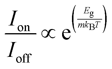 . In both expressions, the parameter m depends on the transistor configuration and its factor ≥2, kB is the Boltzmann constant, and T is the temperature. Ensuring the proper functioning of a logic-FET requires the bandgap of the channel material to be at least 0.4 eV for a sufficiently high Ion/Ioff and effective switching speed.50 The calculated band gap of the pristine ML α-MoTe2 is 1.08 eV, as shown in Fig. 3(a), with both the valence band maximum (VBM) and conduction band minimum (CBM) located at the K-point, confirming its direct band gap nature. Direct band gap materials enable efficient inter-band transitions without requiring phonon assistance, thereby minimizing scattering and enhancing carrier transport and mobility. Quantum confinement effects significantly alter the electronic band structure of the BL α-MoTe2 compared to that of the ML α-MoTe2. The calculated band gap of the BL α-MoTe2 is 0.88 eV, as shown in Fig. 3(b). Unlike the ML counterpart, BL α-MoTe2 exhibits an indirect band gap, with the VBM at the Γ-point and the CBM at the Q-point. Indirect band gap materials enable efficient inter-band transitions, which can lead to increased scattering and lower carrier mobility. Therefore, the ML and BL α-MoTe2 possess an optimal electronic band gap, rendering them promising as channel materials for FETs. Our computed band gap values without spin–orbit coupling (SOC) agree with experimental results. For instance, Ruppert et al.51 and Lezama et al.52 reported an experimental band gap of approximately 1.10 eV for monolayer α-MoTe2 (direct K → K) and a reduced indirect band gap (Γ → Q) in the range of 0.85–0.95 eV for bilayer α-MoTe2. Thus, our DFT results reproduce the direct-to-indirect band gap crossover and align well with available experimental data, validating the reliability of our computational framework.
 | ||
| Fig. 3 Calculated electronic band structure of the (a) ML and (b) BL α-MoTe2 without SOC. The nature of the band gap is tuned from a direct one in the ML to an indirect one in the BL case. | ||
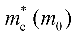
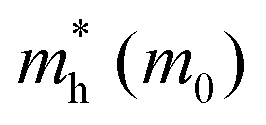
In solids, the effective mass (m*) is a quantity used to simplify the analysis of electronic band structures by approximating the behaviour of a free particle possessing the same mass. The effective mass of electrons  and holes
  is a key parameter in the channel material governing charge carrier mobility and the transport properties in FET devices.53 We computed the carrier effective masses along the transport direction at the K, Γ, and the Q-valley of the conduction band minimum (CBM) and valence band maximum (VBM) of the ML and BL α-MoTe2. The effective mass is calculated using the standard parabolic band approximation, expressed as:
  , where ℏ is the reduced Planck constant, E is the energy, and k is the wave vector. The calculated values of
  and
and  are reported in Table 1. The notable difference in hole effective masses between monolayer (–0.688 m0) and bilayer (–2.894 m0) α-MoTe2 arises from interlayer coupling effects that modify the valence band structure, as shown in Fig. 3. In the monolayer, strong in-plane Mo-d and Te-p orbital interactions yield a highly curved valence band and lower effective mass, while in the bilayer, interlayer Te-Te interactions flatten the band through hybridization, resulting in a much higher effective mass.
 and holes
  of the ML and BL α-MoTe2 along the transport direction at the K, Γ, and the Q-valley of the CBM and VBM
| System | Type | Transport direction |
|
|
|---|---|---|---|---|
| ML | Electron | CBM K-valley | 0.584 | — |
| Hole | VBM K-valley | — | −0.688 | |
| BL | Electron | CBM Q-valley | 0.443 | — |
| Hole | VBM Γ-valley | — | −2.894 |
The carrier mobility μ is related to the effective mass (m*), expressed as 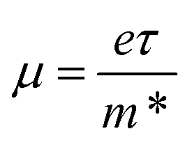 , where e is the elementary charge (e = 1.602 × 10⁻¹⁹ C), and τ is the scattering time. It is evident from the expression of μ that large m* along the transport directions will reduce carrier mobility, thereby hindering the conduction current.
3.2. Transfer IV-characteristics of the ML and BL α-MoTe2 MOSFET
The transfer IV-characteristics are essential in quantum transport simulations for evaluating and analysing the most relevant electrical characteristics of FET device models, including Ion, Ioff, Ion/Ioff, SS, transconductance (gm), and drain-induced barrier lowering (DIBL). The transfer IV-characteristics of the n- and p-type ML α-MoTe2 MOSFET are calculated for HP and LP application, as shown in Fig. 4. To accurately capture the subthreshold region of the 0.34-nm Lg n- and p-type ML α-MoTe2 device under varying LUL, the gate-to-source voltage (Vgs) is swept from −2 V to 0 V for the n-type and from 0 V to 2 V for the p-type. A low Ioff is a key performance indicator, suppressing leakage current and reducing static power dissipation. The Ioff refers to the current flowing when the Vgs is zero and the Vds is set to the supply voltage Vdd. The Ioff and the corresponding Vg (off) are extracted from the transfer IV-characteristics in line with ITRS-2013 projections for the 2028 technology horizon. The benchmark for Ioff is set at 0.01 μA μm−1 for high-performance (HP) devices and 10−4 μA μm−1 for low-power (LP) devices. | ||
| Fig. 4 Transfer IV-characteristics of the 0.34-nm Lg n-type (right panel) and p-type (left panel) ML α-MoTe2 FETs with LUL = 1, 2, and 3 nm. The bias voltage is 0.54 V. The black, short-dashed horizontal lines show the Ioff for HP and LP requirements. | ||
We also simulated the 0.34-nm Lg n- and p-type BL α-MoTe2 MOSFET device and calculated the transfer IV-characteristics with varying LUL as depicted in Fig. 5. Due to the quantum confinement, tunable indirect band gap, and degraded gate-control, the behaviour of the transfer IV-characteristics of the BL α-MoTe2 n and p-type FET significantly differ from that of the ML. In terms of the ITRS-2013 standard projected for 2028 technology horizons, our n- and p-type BL α-MoTe2 transistors failed to meet the standard requirements.
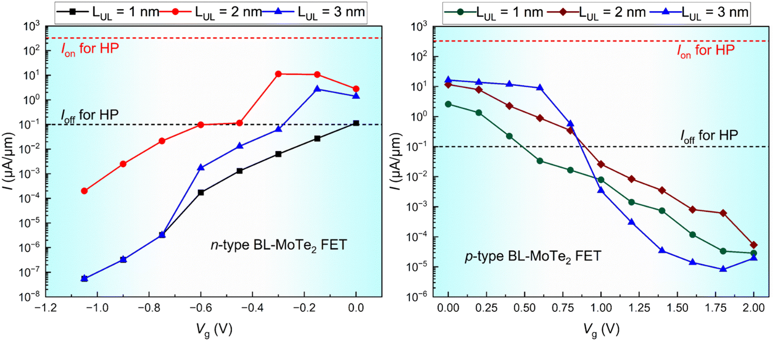 | ||
| Fig. 5 Transfer IV-characteristics of the 0.34-nm Lg BL-α-MoTe2 n-type (left panel) and p-type (right panel) FETs with LUL = 1, 2, and 3 nm. The bias voltage is 0.54 V. The two short-dashed horizontal lines (red and black) correspond to the ITRS requirements of Ion and Ioff for HP. | ||
Based on the transfer IV-characteristics analysis, we evaluated the performance limits of the n- and p-type ML α-MoTe2 FETs featuring the 0.34 nm gate-length. The performance is assessed by calculating the key FOMs, including Ion, SS, τ, and PDP, in line with the projected performance standards for 2028 horizons according to the ITRS-2013.
3.3. The FOMs of the ML α-MoTe2 MOSFET
It is well-recognized that the doping concentration of the source and drain electrodes plays an integral role in determining the performance of FETs.54,55 Considering the tunable bandgap of the α-MoTe2 and the electrostatic influence of the underlap region, it is imperative to optimize the doping concentration to achieve the desired device characteristics at a specific Vg. We analyzed the transfer IV-characteristics of the n- and p-type ML and BL α-MoTe2 FETs under doping concentrations ranging from 1 × 10¹² to 1 × 1014 cm−2, with a Vdd = 0.54 V, as shown in Fig. 6(a). We determined the optimal doping level of 2 × 1013 cm−2 for the n-type ML α-MoTe2 FETs. | ||
| Fig. 6 (a) Impact of doping concentration on Ion for the n- and p-type ML α-MoTe2 FETs, (b) and (c) influence of underlap length (LUL) on Ion for HP and LP applications of the n- and p-type ML α-MoTe2 FETs and (d) impact of LUL on SS for the 0.34-nm Lg n-type ML α-MoTe2 FETs. | ||
The Ion is directly measured from the transfer IV-characteristics with minimal uncertainty, refining it to be the more precise and reliable parameter for evaluating the performance of 2D FETs. The Ion is the source-to-drain current measured at the on-state voltage, Von = Vdd ± Voff, where Vdd expresses the supply-voltage equal to the Vb (bias-voltage), and Voff is the off-state voltage corresponding to Ids = Ioff. The ‘+’ sign applies to the n-type devices, while the ‘−’ sign applies to the p-type devices. The calculated Ion for the n- and p-type ML α-MoTe2 FETs for HP and LP applications with different LUL are reported in Tables 2 and 3. According to the ITRS standard extended to the 0.34-nm Lg device, the value of Ion is 326 μA μm−1 at Vdd = 0.54 V for the HP n- and p-type devices and 57 μA μm−1 for LP device applications. Our n-type ML α-MoTe2 FETs meet the ITRS standards, achieving an Ion of 396 μA μm−1 for HP and 183 μA μm−1 for LP applications, as depicted in Fig. 6(b) and (c).
| Lg (nm) | LUL (nm) | Ioff (μA μm−1) | Ion (μA μm−1) | Ion/Ioff | SS (mV dec−1) | Ct (fF μm−1) | τ (ps) | PDP (fJ μm−1) |
|---|---|---|---|---|---|---|---|---|
| 0.34 | 0 | — | — | — | — | — | — | — |
| 1 | 0.1 | 88 | 8.8 × 10² | 463 | 0.137 | 0.840 | 0.039 | |
| 2 | 0.1 | 396 | 3.96 × 10³ | 151 | 0.244 | 0.334 | 0.071 | |
| 3 | 0.1 | 287 | 2.87 × 10³ | 205 | 0.287 | 0.540 | 0.084 | |
| 0.34 (ITRS) | — | 0.1 | 326 | 3.26 × 10³ | — | 0.26 | 0.424 | 0.07 |
| Lg (nm) | LUL (nm) | Ioff (μA μm−1) | Ion (μA μm−1) | Ion/Ioff | SS (mV dec−1) | Ct (fF μm−1) | τ (ps) | PDP (fJ μm−1) |
|---|---|---|---|---|---|---|---|---|
| 0.34 | 0 | — | — | — | — | — | — | — |
| 1 | 1.09 × 10⁻⁴ | 16 | 1.47 × 10⁵ | 372 | 0.057 | 1.89 | 0.016 | |
| 2 | 1.09 × 10⁻⁴ | 106 | 9.72 × 10⁵ | 146 | 0.215 | 1.075 | 0.060 | |
| 3 | 1.09 × 10⁻⁴ | 183 | 1.68 × 10⁶ | 88 | 0.234 | 0.677 | 0.066 | |
| 0.34 (ITRS) | — | 1.09 × 10⁻⁴ | 59 | 5.41 × 10⁵ | — | 0.26 | 2.354 | 0.07 |
The gate-control is critical for transistor performance, and enhancing this control is a key strategy to mitigate SCEs. It is typically assessed by the SS, a key parameter that characterizes the switching efficiency of a transistor. SS is defined as the gate voltage change needed to increase the drain current by one order of magnitude in the subthreshold region, expressed as  . A smaller SS value signifies a strong gate control, reflecting enhanced performance and efficiency. In ideal transistors, the subthreshold swing is theoretically limited to 60 mV decade−1 at room temperature (300 K). This limit is a consequence of the inherent thermionic emission process of charge carriers, which is governed by the Boltzmann distribution.56 Fig. 6(d) shows the impact of LUL on SS for the 0.34-nm Lg n-type ML α-MoTe2 FETs. The minimum value of the SS for the HP n-type ML α-MoTe2 FETs is 151 mV dec−1 achieved at LUL = 2 nm, and for LP is 88 mV dec−1 at LUL = 3 nm. These results highlight the importance of LUL in optimizing gate controllability for the 0.34-nm Lg n-type ML α-MoTe2 FETs. These minimum SS values indicate improved gate-control and switching efficiency, with enhanced performance for HP and LP devices at their optimal LUL values.
Since the ITRS standard is only a reference, we also compare our n-type device performance in terms of Ion and SS with other ab initio simulation results for the most studied 2D material-based transistors with Lg ≤ 1 nm, as illustrated in Fig. 7. The scattered data in the figure shows that the Ion of our n-type ML α-MoTe2 FETs is comparable to that of the widely studied ML MoS2 FETs at the sub-1 nm Lg. The SS values for our device demonstrate promising switching characteristics, though still slightly higher than those observed in the MoS2 FETs, suggesting potential for further optimization in switching efficiency.
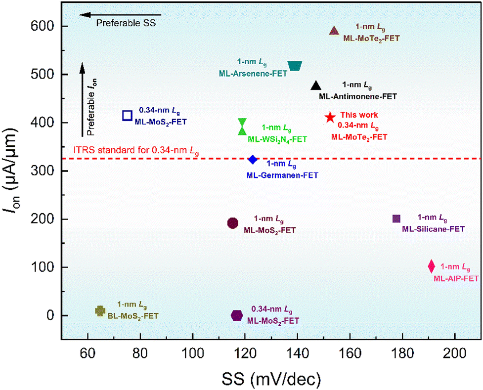 | ||
| Fig. 7 Comparison of the Ion and SS of the n-type 0.34-nm Lg ML-MoTe2-FET (this work) with other most studied 2D material-based transistors scaling with Lg ≤ 1 nm.57–62 The red short-dashed horizontal line represents the ITRS standard for Ion with the Lg of 0.34 nm. The black solid vertical arrow is directed upward, and the horizontal arrow is directed leftward, displaying that high Ion and low SS values are preferable for the best performance of FETs. | ||
To further explore the gate control mechanism, we analyze the projected local device density of states (PLDOS) of the ML n-type transistor with LUL of 2-nm under both off- and on-state Vg conditions. The PLDOS plots illustrate the spatially resolved electronic states along the transport direction (z-axis) of the ML α-MoTe2 FET, as shown in Fig. 8(a) and (b). The energy-resolved local density of states (LDOS) is color-coded, where black indicates low density and pink indicates high density of electronic states. To estimate the potential barrier height (ΦB) in both the off-state and on-state from the PLDOS, we analyze the conduction band profile above the Fermi level (yellow contour line) in the channel region, particularly where the band reaches its maximum along the transport direction (z-axis).
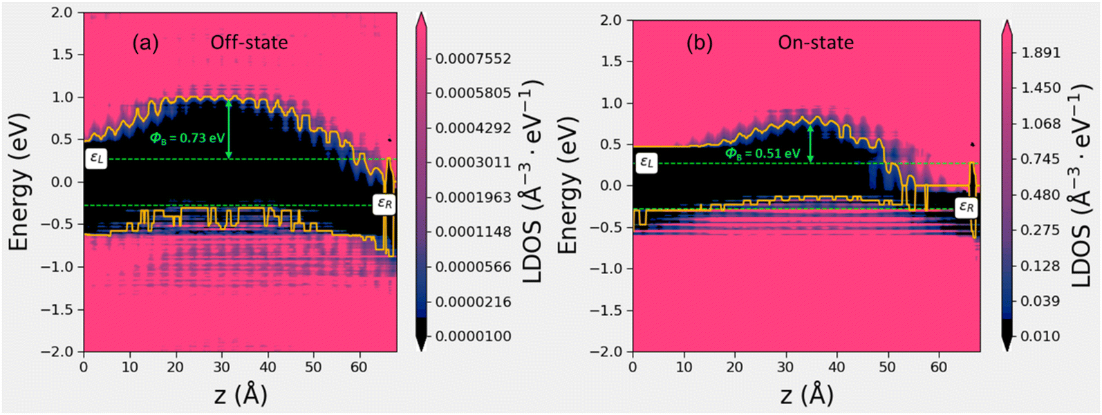 | ||
| Fig. 8 Computed PLDOS of the 0.34-nm Lg n-type ML α-MoTe2 FETs with LUL = 2 nm in the off-state (a) and on-state (b). The Vdd is 0.54 V, and the Vg for the off and on-state is −0.41 V and 0.13 V, respectively. εL and εR depict the chemical potential of the left and right electrode. | ||
The conduction band edge in the off-state exhibits a pronounced energy barrier between the source and drain, effectively suppressing the carrier injection across the channel. This barrier potential shows a direct consequence of the gate-induced electrostatics. It creates a difference in the chemical potential (εL) of the source, i.e., the left electrode and the available conduction states in the channel, resulting in minimal carrier transmission and, thus, a low Ioff. In the off-state, the conduction band peaks at approximately 0.73 eV above the εL, resulting in an estimated barrier height of 0.73 eV. The applied Vdd of 0.54 V introduces a potential drop across the channel, seen as an energy difference between εL and εR. The extent of the barrier modulation between the off- and on-states is a critical indicator of gate control, essential for achieving a high Ion/Ioff current ratio and optimal subthreshold performance in ultra-scaled FETs.
In contrast, the on-state PLDOS plot shows a substantial barrier lowering, with the conduction band aligning closer to εL and εR. In the on-state, the conduction band is significantly lowered, with the peak positioned approximately 0.51 eV above εL, resulting in an estimated barrier height of 0.51 eV. This electrostatic modulation flattens the potential barrier across the channel, enabling efficient carrier transport and resulting in a significantly higher Ion. These values of ΦB at the off and on-state show a strong gate-induced modulation (∼0.22 eV barrier lowering), indicative of excellent electrostatic control in the ultra-scaled 0.34-nm ML MoTe2 FET.
In addition to Ion and SS, we investigated two other key performance indicators: intrinsic delay-time (τ) and power dissipation (PDP). In the context of FETs, the τ represents the time it takes for a transistor to switch from one state (on or off) to another, typically from the off-state to the on-state. Shorter τ indicates faster switching speeds, crucial for high-speed electronics such as processors and communication devices. The τ is influenced by factors like the capacitance of the gate (Cg), Ion, and Vdd, expressed as:  . The Ct = 3Cg, and Cg is expressed as;
 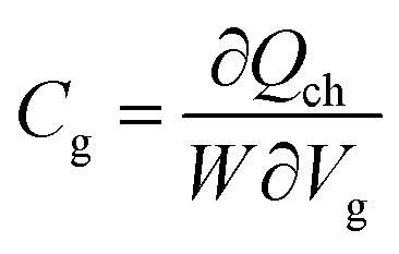 , where Qch shows the total charge accumulated in the central channel region under Vdd of 0.54 V, and W is the width of the device. The calculated τ for the 0.34-nm Lg n-type ML α-MoTe2 FETs with optimized LUL = 2 nm is 0.334 ps for HP and 1.075 ps for LP. These values satisfy the ITRS standard, as reported in Tables 2 and 3.
PDP is a critical FOM for assessing speed and power consumption trade-offs. PDP is determined as the product of the power consumed (P) and the τ during the one switching operation and is formulated as PDP = τP = CtV2dd. Since the Vdd is 0.54 V, the PDP is primarily influenced by the Ct. A lower PDP is desired because it indicates a transistor that can switch faster while consuming less power. The calculated PDP numerical values for our n-type ML α-MoTe2 FETs with optimized LUL = 2 nm are 0.071 fJ μm−1 for HP and 0.060 fJ μm−1 for LP applications, meet the ITRS standard and are reported in Tables 2 and 3.
4. Conclusion
In conclusion, this research utilized the DFT + NEGF formalism for quantum transport simulation to evaluate the performance limit of the n- and p-type sub-1 nm gate-length ML and BL α-MoTe2 FETs for HP and LP applications. The FETs are simulated under an ultra-low bias voltage of 0.54 V. The n-type ML α-MoTe2 FETs meet the requirements of the ITRS standard for HP and LP devices in terms of Ion [396 μA μm−1 (HP) and 183 μA μm−1 (LP)], τ[0.334 ps (HP) and 1.075 ps (LP)] and PDP [0.071 fJ μm−1 (HP) and 0.060 fJ μm−1 (LP)]. The p-type ML and the n- and p-type BL α-MoTe2 transistors fail to meet the ITRS requirements for HP and LP devices because of the high effective mass of holes. The minimum SS for the HP n-type ML α-MoTe2 FETs is 151 mV dec−1, and that for the LP is 88 mV dec−1. The findings presented here represent a significant step toward developing the n-type sub-1 nm gate-length FETs based on the ML α-MoTe2.Author contributions
Mudasser Husain: conceptualization, methodology, software, investigation, data curation, formal analysis, writing – original draft, writing – review and editing. Younas Ahmed: visualization. Xingyue Yang: methodology, validation. Shibo Fang: formal analysis, conceptualization. Zongmeng Yang: data curation, validation. Jichao Dong: visualization. Linqiang Xu: methodology, visualization. Nasir Rahman: formal analysis. Jing Lu: conceptualization, writing – review and editing, funding acquisition, project administration, resources, supervision, validation, visualization.Conflicts of interest
The authors declare no competing financial interest.Data availability
The data supporting the findings of this study are available from the corresponding author upon reasonable request.Acknowledgements
This work was supported by the National Natural Science Foundation of China (No. 12274002 and 91964101), the Ministry of Science and Technology of China (No. 2022YFA1203904), the Fundamental Research Funds for the Central Universities, the High-performance Computing Platform of Peking University and the MatCloud + high throughput materials simulation engine. S. Fang is supported by the National Research Foundation, Singapore, under its Frontier Competitive Research Programme (NRF-F-CRP-2024-0001). We thank Y. S. A. for insightful discussions.References
- A. Pal, T. Chavan, J. Jabbour, W. Cao and K. Banerjee, Three-dimensional transistors with two-dimensional semiconductors for future CMOS scaling, Nat. Electron., 2024, 7(12), 1147–1157 CrossRef CAS
.
- R. R. Schaller, Moore's law: past, present and future, IEEE Spectr., 1997, 34(6), 52–59 Search PubMed
- D. Bhattacharya and N. K. Jha, FinFETs: From devices to architectures, Adv. Electron., 2014,(1), 365689 Search PubMed
- A. Razavieh, P. Zeitzoff and E. J. Nowak, Challenges and limitations of CMOS scaling for FinFET and beyond architectures, IEEE Trans. Nanotechnol., 2019, 18, 999–1004 CAS
- S. Liu, et al., Can ultra-thin Si FinFETs work well in the sub-10 nm gate-length region?, Nanoscale, 2021, 13(10), 5536–5544 RSC
- X. Wang, C. Liu, Y. Wei, S. Feng, D. Sun and H. Cheng, Three-dimensional transistors and integration based on low-dimensional materials for the post-Moore's law era, Mater. Today, 2023, 63, 170–187 CrossRef CAS
- Q. Zhang, Y. Zhang, Y. Luo and H. Yin, New structure transistors for advanced technology node CMOS ICs, Natl. Sci. Rev., 2024, 11(3), nwae008 CrossRef CAS PubMed
- P. S. Dhanaselvam, B. Karthikeyan and P. Anand, Future Prospective Beyond CMOS Technology Design, Graphene Field-Eff. Transistors, 2025, 73–80 Search PubMed
- K. S. Kim, et al., The future of two-dimensional semiconductors beyond Moore's law, Nat. Nanotechnol., 2024, 19(7), 895–906 CrossRef CAS PubMed
- S. Zeng, C. Liu and P. Zhou, Transistor engineering based on 2D materials in the post-silicon era, Nat. Rev. Electr. Eng., 2024, 1–14 Search PubMed
- Y. Shen, et al., The trend of 2D transistors toward integrated circuits: scaling down and new mechanisms, Adv. Mater., 2022, 34(48), 2201916 CrossRef CAS PubMed
- S. B. Mitta, et al., Electrical characterization of 2D materials-based field-effect transistors, 2D Mater., 2020, 8(1), 12002 CrossRef
- M. Chhowalla, D. Jena and H. Zhang, Two-dimensional semiconductors for transistors, Nat. Rev. Mater., 2016, 1(11), 1–15 Search PubMed
- Y. Tan, et al., Controllable 2H-to-1T′ phase transition in few-layer MoTe2, Nanoscale, 2018, 10(42), 19964–19971 RSC
- W. Cao, et al., The future transistors, Nature, 2023, 620(7974), 501–515 CrossRef CAS PubMed
- M. Husain, N. Rahman and J. Lu, Quantum transport simulations of monolayer β-AgI: a prospective nanochannel material in sub-1 nm gate-length MOSFETs, Nanoscale, 2025, 17(12), 7367–7378 RSC
- F. Wu, et al., Vertical MoS2 transistors with sub-1-nm gate lengths, Nature, 2022, 603(7900), 259–264 CrossRef CAS PubMed
- Y. Li et al., Quantum Transport Simulation of Sub-1-nm Gate Length Monolayer MoS2 Transistors, arXiv, 2024, preprint, arXiv2404.13801 DOI:10.48550arXiv2404.13801.
- X. Yang, et al., Ab-Initio Quantum Transport Simulation of Sub-1 nm Gate Length Monolayer and Bilayer WSe2 Transistors: Implications for Ultra-Scaled CMOS Technology, ACS Appl. Nano Mater., 2025, 8, 3460–3470 CrossRef CAS
- J. Cai, et al., High-performance complementary circuits from two-dimensional MoTe2, Nano Lett., 2023, 23(23), 10939–10945 CrossRef CAS PubMed
- M. J. Mleczko, et al., Contact engineering high-performance n-type MoTe2 transistors, Nano Lett., 2019, 19(9), 6352–6362 CrossRef CAS PubMed
- S. Meena, N. Sharma and J. Jogi, Sub-5 nm 2D Semiconductor-Based Monolayer Field-Effect Transistor: Status and Prospects, Phys. Status Solidi, 2023, 220(11), 2200526 CrossRef CAS
- Q. Zhang, et al., Simultaneous synthesis and integration of two-dimensional electronic components, Nat. Electron., 2019, 2(4), 164–170 CrossRef
- Q. Li, et al., Sub-5 nm gate length monolayer MoTe2 transistors, J. Phys. Chem. C, 2021, 125(35), 19394–19404 CrossRef CAS
- Y. Wang, et al., Schottky barrier heights in two-dimensional field-effect transistors: from theory to experiment, Rep. Prog. Phys., 2021, 84(5), 56501 CrossRef CAS PubMed
- International Technology Roadmap for Semiconductors (ITRS), Semiconductor Research Corporation, 2013, https://www.semiconductors.org/resources/2013-international-technology-roadmap-for-semiconductors-itrs/.
- B. Hoefflinger, ITRS 2028—International roadmap of semiconductors, CHIPS 2020 VOL. 2 New Vistas Nanoelectronics, 2016, pp. 143–148 Search PubMed
- M. Salmani-Jelodar, H. Ilatikhameneh, S. Kim, K. Ng, P. Sarangapani and G. Klimeck, Optimum high-k oxide for the best performance of ultra-scaled double-gate MOSFETs, IEEE Trans. Nanotechnol., 2016, 15(6), 904–910 CAS
- M. A. Ahmad and J. Kumar, The understanding of the impact of efficiently optimized underlap length on analog/RF performance parameters of GNR-FETs, Sci. Rep., 2023, 13(1), 13872 CrossRef CAS PubMed
- S. Smidstrup, et al., QuantumATK: an integrated platform of electronic and atomic-scale modelling tools, J. Phys.: Condens. Matter, 2019, 32(1), 15901 CrossRef PubMed
- D. Stradi, U. Martinez, A. Blom, M. Brandbyge and K. Stokbro, General atomistic approach for modeling metal-semiconductor interfaces using density functional theory and nonequilibrium Green's function, Phys. Rev. B, 2016, 93(15), 155302 CrossRef
- S. Smidstrup, et al., First-principles Green's-function method for surface calculations: A pseudopotential localized basis set approach, Phys. Rev. B, 2017, 96(19), 195309 CrossRef
- J. P. Perdew, K. Burke and M. Ernzerhof, Generalized gradient approximation made simple, Phys. Rev. Lett., 1996, 77(18), 3865 CrossRef CAS PubMed
- P. Borlido, J. Doumont, F. Tran, M. A. L. Marques and S. Botti, Validation of pseudopotential calculations for the electronic band gap of solids, J. Chem. Theory Comput., 2020, 16(6), 3620–3627 CrossRef CAS PubMed
- S. Ju, B. Liang, J. Zhou, D. Pan, Y. Shi and S. Li, Coulomb screening and scattering in atomically thin transistors across dimensional crossover, Nano Lett., 2022, 22(16), 6671–6677 CrossRef CAS PubMed
- K. Walzer, B. Maennig, M. Pfeiffer and K. Leo, Highly efficient organic devices based on electrically doped transport layers, Chem. Rev., 2007, 107(4), 1233–1271 CrossRef CAS PubMed
- X. Zhang, Z. Shao, X. Zhang, Y. He and J. Jie, Surface charge transfer doping of low-dimensional nanostructures toward high-performance nanodevices, Adv. Mater., 2016, 28(47), 10409–10442 CrossRef CAS PubMed
- S. Tsuzuki and T. Uchimaru, Accuracy of intermolecular interaction energies, particularly those of hetero-atom containing molecules obtained by DFT calculations with Grimme's D2, D3 and D3BJ dispersion corrections, Phys. Chem. Chem. Phys., 2020, 22(39), 22508–22519 RSC
- J. Xie, et al., Gate switchable spin-orbit splitting in a MoTe 2/WTe 2 heterostructure from first-principles calculations, Phys. Rev. B, 2023, 107(16), 165101 CrossRef CAS
- N. R. Pradhan, et al., Field-effect transistors based on few-layered α-MoTe2, ACS Nano, 2014, 8(6), 5911–5920 CrossRef CAS PubMed
- S. Datta, Quantum transport: atom to transistor, Cambridge University Press, 2005 Search PubMed
- Y. M. Sabry, T. M. Abdolkader and W. F. Farouk, Simulation of quantum transport in double-gate MOSFETs using the non-equilibrium Green's function formalism in real-space: a comparison of four methods, Int. J. Numer. Model. Electron. Netw. Devices Fields, 2011, 24(4), 322–334 CrossRef
- M. Pourfath, The non-equilibrium Green's function method for nanoscale device simulation, Springer, 2014, vol. 3 Search PubMed
- H. M. Pastawski, Classical and quantum transport from generalized Landauer-Büttiker equations, Phys. Rev. B: Condens. Matter Mater. Phys., 1991, 44(12), 6329 CrossRef PubMed
- K. Khan, et al., Recent developments in emerging two-dimensional materials and their applications, J. Mater. Chem. C, 2020, 8(2), 387–440 RSC
- S. Das, et al., Transistors based on two-dimensional materials for future integrated circuits, Nat. Electron., 2021, 4(11), 786–799 CrossRef CAS
- J. Hafner, Ab-initio simulations of materials using VASP: Density-functional theory and beyond, J. Comput. Chem., 2008, 29(13), 2044–2078 CrossRef CAS PubMed
- A. Togo, First-principles phonon calculations with phonopy and phono3py, J. Phys. Soc. Japan, 2023, 92(1), 12001 CrossRef
- T. Tan, X. Jiang, C. Wang, B. Yao and H. Zhang, 2D material optoelectronics for information functional device applications: status and challenges, Adv. Sci., 2020, 7(11), 2000058 CrossRef CAS PubMed
- E. L. Wolf and E. L. Wolf, Graphene Logic Devices and Moore's Law, Appl. Graphene An Overv., 2014, 51–67 Search PubMed
- C. Ruppert, B. Aslan and T. F. Heinz, Optical properties and band gap of single-and few-layer MoTe2 crystals, Nano Lett., 2014, 14(11), 6231–6236 CrossRef CAS PubMed
- I. G. Lezama, et al., Indirect-to-direct band gap crossover in few-layer MoTe2, Nano Lett., 2015, 15(4), 2336–2342 CrossRef CAS PubMed
- Y. Liu, X. Duan, H.-J. Shin, S. Park, Y. Huang and X. Duan, Promises and prospects of two-dimensional transistors, Nature, 2021, 591(7848), 43–53 CrossRef CAS PubMed
- R. Kim, U. E. Avci and I. A. Young, Source/drain doping effects and performance analysis of ballistic III-V n-MOSFETs, IEEE J. Electron Devices Soc., 2014, 3(1), 37–43 Search PubMed
- Y. Zhao, K. Xu, F. Pan, C. Zhou, F. Zhou and Y. Chai, Doping, contact and interface engineering of two-dimensional layered transition metal dichalcogenides transistors, Adv. Funct. Mater., 2017, 27(19), 1603484 CrossRef
- Y. Zhai, Z. Feng, Y. Zhou and S.-T. Han, Energy-efficient transistors: suppressing the subthreshold swing below the physical limit, Mater. Horiz., 2021, 8(6), 1601–1617 RSC
- X. Sun, et al., Sub-5 nm monolayer arsenene and antimonene transistors, ACS Appl. Mater. Interfaces, 2018, 10(26), 22363–22371 CrossRef CAS PubMed
- W. A. Abdul-Hussein, F. H. Hanoon and L. F. Al-Badry, Designing sub-5 nm monolayer AlP MOSFETs, Micro Nanostruct., 2023, 176, 207524 CrossRef CAS
- S. B. Desai, et al., MoS2 transistors with 1-nanometer gate lengths, Science, 2016, 354(6308), 99–102 CrossRef CAS PubMed
- Y. Li, et al., Monolayer WSi 2 N 4: A promising channel material for sub-5-nm-gate homogeneous CMOS devices, Phys. Rev. Appl., 2023, 20(6), 64044 CrossRef CAS
- Y. Pan, et al., Sub-5-nm monolayer silicane transistor: A first-principles quantum transport simulation, Phys. Rev. Appl., 2020, 14(2), 24016 CrossRef CAS
- L. Xu, et al., Performance limits exploration of sub-5 nm monolayer germanane transistors: A first-principle quantum transport simulation, J. Appl. Phys., 2024, 135, 134303 CrossRef CAS
| This journal is © The Royal Society of Chemistry 2025 |