
Dual-Schottky heteroepitaxial Nb:SrTiO3/TiN/Si for high-performance broadband photodetection across the UV–IR spectrum
Minghao Hu,
Tianyu Cai,
Weiqiang Yang,
Bin Yue,
Anran Niu,
Bingbing Li and
Wenfeng Xiang *
*
College of New Energy and Materials, China University of Petroleum, Beijing, 102249, China. E-mail: wfxiang@cup.edu.cn
First published on 5th August 2025
Abstract
Broadband photodetectors with spectral response ranging from ultraviolet (UV) to infrared (IR) are of great significance for various applications. However, conventional silicon-based photodetectors exhibit low response efficiency in the UV region. Although heterojunction structures can extend the spectral response range through material synergy, they still face challenges such as poor stability and insufficient absorption efficiency. In this study, an Nb:SrTiO3/TiN/Si heteroepitaxial structure was fabricated on a silicon substrate using pulsed laser deposition. The crystal structure, interface quality, and compositional distribution of the materials were characterized. The spectral response characteristics were evaluated using a photoelectric testing system. Experimental results demonstrate that the TiN buffer layer effectively reduces the lattice mismatch between Nb:SrTiO3 and Si while enhancing interfacial charge transport through its metallic properties and localized surface plasmon resonance effect. The Nb:SrTiO3/TiN/Si heterojunction achieves the responsivity values of 2.14 V W−1, 1.34 V W−1, and 4.1 V W−1 under 808 nm, 532 nm, and 365 nm illumination, respectively, significantly outperforming the TiN/Si structure. The dual-Schottky junction mechanism—where the Si/TiN junction dominates IR/visible response and the NbSTO/TiN junction facilitates UV carrier separation—enables balanced photodetection from UV to IR. Additionally, the photoconductive effect under 248 nm pulsed light confirms the broadband response capability of the heterostructure. This study not only provides a novel material design strategy for optimizing the performance of silicon-based photodetectors but also establishes an experimental foundation for developing high-performance broadband photodetectors.
Introduction
Photodetectors (PDs), as crucial optoelectronic devices, hold significant application value in broadband detection spanning from ultraviolet (UV) to infrared (IR) wavelengths.1–3 In particular, PDs with full-spectrum response capabilities demonstrate broad application prospects in fields such as imaging sensing, optical communications, environmental monitoring, and civil engineering.4–7 Currently, commercial silicon-based photodetectors (Si PDs) have become the mainstream choice in the market due to their broadband response (400–1100 nm), high reliability, and mature low-cost manufacturing processes.8,9 However, the detection performance of Si PDs in the ultraviolet range (300–400 nm) remains notably limited: constrained by silicon's high reflectivity and shallow penetration depth for UV light; their external quantum efficiency (EQE) typically falls below 20%, significantly lower than their response levels in the visible to infrared (Vis-IR) range.10–12 Although various optimization strategies (such as surface passivation and anti-reflection coatings) have been implemented, achieving balanced high-performance response in both UV and Vis-IR bands for Si PDs remains a critical challenge in the current field of photodetection.7,13In recent years, heterojunction structures have made significant progress in broadening the spectral response range of photodetectors through synergistic effects among materials with different wavelength responses.13–21 For instance, quantum dot heterojunctions combined with quantum cutting luminescent concentrators can effectively enhance detection capabilities in the ultraviolet range (200–400 nm), while composite structures of narrow-bandgap organic materials and perovskite quantum dots can further extend the infrared response range (700–1000 nm).13–18 Additionally, heterojunctions of perovskites and semiconductor materials (e.g., Ge or Si) enable continuous detection from visible to infrared wavelengths through complementary band alignment.19–21 However, these heterojunction structures still face several critical challenges: quantum dot materials exhibit high trap density and poor carrier mobility, along with sensitivity to moisture and UV radiation, severely limiting the stability of their broadband response.15 Although heterojunctions formed between two-dimensional materials (e.g., graphitic carbon nitride, g-CN) and silicon achieve broadband detection from ultraviolet to infrared (300–1100 nm) via the lateral photovoltaic effect, their UV-visible absorption efficiency remains to be improved due to the inherent limitation of nanoscale thickness.22–26
Building upon the TiO2/Ag/SrSO4 heterojunction system developed by Liu et al. which achieves efficient photogenerated carrier separation and broadband spectral energy utilization through the synergistic effects of localized surface plasmon resonance (LSPR) from Ag nanoparticles and directional electron transport in SrSO4),27 and leveraging our previous research on TiN/Si interfaces,28 this study employed pulsed laser deposition to fabricate an epitaxial Nb:SrTiO3 (NbSTO)/TiN/Si dual-heterojunction structure on silicon substrates. In this architecture, the TiN interlayer serves dual functions: (1) as a lattice-mismatch buffer to reduce interfacial defects between NbSTO and Si, (2) as a plasmonic component analogous to Ag nanoparticles, enhancing photogenerated electron trapping and transport through its metallic conductivity and LSPR effects. Unlike conventional heterojunctions relying on quantum dots or organic–inorganic hybrids (which often suffer from poor stability or low carrier mobility), this epitaxial design combines the wide-bandgap advantages of NbSTO (for UV response) with the mature optoelectronic properties of silicon (for visible-IR detection), while the TiN layer optimizes interfacial charge transport for synergistic enhancement. Experimental results demonstrate that compared to the TiN/Si single heterojunction, this dual-heterojunction system exhibits superior full-spectrum response characteristics, though further systematic studies are required to elucidate the wavelength-dependent response mechanisms. By integrating epitaxial oxide growth with plasmonic engineering, this work provides a new strategy for developing silicon-compatible, high-performance broadband photodetectors covering UV to IR wavelengths.
Results and discussion
The XRD patterns of the NbSTO/TiN/Si and TiN/Si heteroepitaxial structures are shown in Fig. 1a, where all diffraction peaks can be well indexed to TiN (JCPDS no. 38-1420) and SrTiO3 (JCPDS no. 35-0724). Both samples exhibit only the (l00) diffraction peaks of NbSTO and TiN films without any impurity peaks, confirming their cubic-phase structure. Notably, compared with the TiN/Si heterostructure, the TiN (200) diffraction peak in the NbSTO/TiN/Si heterostructure exhibits a slight shift toward higher angles, which may be attributed to the relatively large lattice mismatch (∼7.5%) between NbSTO and TiN. Fig. 1b presents the cross-sectional HRTEM image of the NbSTO/TiN/Si heterostructure. The image clearly reveals continuous and well-aligned lattice fringes across all layers, without observable amorphous regions or dislocation clusters, confirming the single-crystalline nature of the epitaxially grown materials. As highlighted in the insets, the yellow- and blue-bordered regions correspond to FFT-enhanced lattice fringe reconstructions (performed in Digital Micrograph) of the NbSTO (100) and TiN (200) lattice planes, respectively. The calculated d spacings—for NbSTO (100) at 0.390 nm and TiN (200) at 0.210 nm—exhibit excellent agreement with reference lattice constants.29 Furthermore, both the NbSTO/TiN and TiN/Si interfaces exhibit atomically sharp contact characteristics without detectable lattice distortion or interdiffusion layers. The TiN buffer layer with a thickness of approximately 16 nm effectively mitigates the lattice mismatch between NbSTO and Si. The uniform strain field distribution in the interfacial transition region indicates an efficient stress relaxation mechanism, which provides favorable conditions for charge carrier transport in subsequent device applications. Fig. 1c presents the AFM characterization of the NbSTO thin film surface morphology. The measured root-mean-square (RMS) surface roughness of 0.447 nm over a 5 μm × 5 μm scan area confirms atomic-level smoothness. Notably, the surface shows a complete absence of particulate or island features, indicating a good two-dimensional growth uniformity. The RBS analysis of the NbSTO/TiN/Si heterostructure was shown in Fig. 1d. The RBS spectrum reveals the NbSTO layer exhibits an oxygen-deficient SrTi1.05O2.5 stoichiometry, and the TiN buffer layer shows a slightly Ti-deficient Ti0.96N composition. Most notably, the oxygen deficiency in the NbSTO film provides direct evidence of substantial oxygen vacancy formation during growth.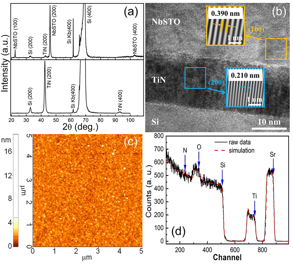 | ||
| Fig. 1 (a) XRD patterns of the NbSTO/TiN/Si and TiN/Si heterostructures. (b) HRTEM images, (c) AFM images and (d) RBS spectrum of the NbSTO/TiN/Si heterostructure, respectively. | ||
Fig. 2 presents a comparative analysis of the UV–IR reflectance spectra between NbSTO/TiN/Si and TiN/Si heterostructures across the 200–1000 nm wavelength range. The NbSTO/TiN/Si heterostructure exhibits three distinct optical characteristics: (1) a characteristic absorption peak at 346 nm (3.58 eV), with energy slightly higher than the bandgap of NbSTO (3.26 eV), potentially attributed to the Burstein–Moss effect-induced apparent blue shift;30–33 (2) a distinct absorption peak observed at 820 nm is completely absent in the TiN/Si control sample, which can be attributed to the localized surface plasmon resonance (LSPR) effect of the TiN layer. Studies have shown that the excitation of LSPR in TiN thin films relies on specific dielectric environment design, with its physical mechanism rooted in the local field confinement induced by dielectric constant matching.34 Notably, the TiN/Si structure alone fails to generate the LSPR effect, whereas the NbSTO/TiN/Si heterostructure successfully achieves this phenomenon. This significant difference stems from the gradient dielectric environment constructed by the NbSTO overlayer, whose unique structure effectively facilitates the formation of localized resonance conditions; (3) a notable enhancement of reflectance in the 400–600 nm visible range, resulting from the gradient refractive index structure formed at the NbSTO/TiN interface that modulates the optical field. These results demonstrate that the NbSTO layer not only contributes intrinsic bandgap absorption but also activates the plasmonic effects of TiN through interfacial coupling, synergistically optimizing the optical performance of the heterostructure.
 | ||
| Fig. 2 Reflection spectra of the NbSTO/TiN/Si and TiN/Si heterostructures. | ||
Fig. 3a–c show the open-circuit photovoltage curves of NbSTO/TiN/Si and TiN/Si heterojunctions under illumination with an 808 nm laser, a 532 nm laser, and a 365 nm mercury lamp. The NbSTO/TiN/Si heterojunction exhibits significant photovoltaic responses across all three wavelengths: under the 808 nm laser with a power density of 1.14 mW cm−2, the photovoltage reaches 193 mV with a corresponding photoresponsivity of 2.14 V W−1, while the 532 nm laser generates 121 mV of photovoltage with a photoresponsivity of 1.34 V W−1, with the former being approximately 60% higher than the latter. Under the 365 nm mercury lamp illumination at 0.31 mW cm−2, the photovoltage achieves 100.2 mV, and the corresponding photoresponsivity is 4.1 V W−1. In contrast, the TiN/Si heterojunction exhibits notably weaker photovoltaic performance: it shows only about 30 mV response under 532 nm laser, minimal response (approximately 0.2 mV) under 808 nm laser, and almost no photovoltaic effect under 365 nm mercury lamp light. These results indicate that the NbSTO/TiN/Si heterojunction responds better to infrared light (808 nm) than to visible light (532 nm), while also demonstrating efficient conversion capability for ultraviolet light (365 nm). Furthermore, the introduction of the NbSTO layer significantly enhances the broadband spectral response performance of the heterojunction.
 | ||
| Fig. 3 Transient photovoltage responses of NbSTO/TiN/Si and TiN/Si heterostructures under illumination at three wavelengths: (a) 808 nm, (b) 532 nm, and (c) 365 nm, respectively. | ||
Fig. 4a and b present the open-circuit photovoltage spectra of the NbSTO/TiN/Si heterojunction under 808 nm and 532 nm laser irradiation at different power densities. The results demonstrate a stable increasing trend in photovoltage peaks with rising power density, while maintaining notable consistency across different power densities, confirming the heterojunction's stable photoelectric conversion performance in both infrared and visible light bands. The power density-photovoltage relationship curve in Fig. 4c reveals the characteristic variation pattern of photovoltage with light intensity: in the low power density range (0.26–0.4 mW cm−2), the photovoltage under 808 nm and 532 nm laser irradiation increases from 35 mV to 135 mV and from 7 mV to 88 mV, respectively, showing an approximately linear growth trend. However, in the higher power density range (0.5–1.14 mW cm−2), the photovoltage increase slows significantly, rising only from 156 mV to 196 mV (808 nm) and from 105 mV to 122 mV (532 nm), exhibiting typical saturation behavior. This characteristic transition from linear growth to saturation originates from the dynamic equilibrium between photocarrier generation and collection. At low light intensities, the number of photocarriers is proportional to incident photon flux, allowing the built-in electric field to effectively separate carriers. As light intensity increases, enhanced carrier recombination and the limited collection capacity of the depletion region electric field collectively lead to the observed saturation phenomenon in photovoltage.
 | ||
| Fig. 4 Transient photovoltage responses with different light power density at (a) 808 nm and (b) 532 nm of the NbSTO/TiN/Si heterostructure, respectively. (c) Photovoltage variation as a function of the light power density. | ||
Fig. 5 presents the study on the photoconductive effect characteristics of the NbSTO/TiN/Si heterojunction under 248 nm pulsed illumination (0.4 mW cm−2). A schematic diagram of the test setup is shown in the inset of Fig. 5b. Experimental observations reveal that as the applied bias voltage increases from 5 V to 13 V, the peak voltage signal across the 100 Ω resistor exhibits an increase from 37 mV to 51 mV. This phenomenon elucidates the voltage-dependent mechanism of the photoconductive effect: under 248 nm laser irradiation, the separation efficiency of photogenerated carriers in the heterojunction is significantly enhanced by the applied electric field, while the carrier recombination process is suppressed. Consequently, the photocurrent intensifies with increasing applied bias voltage, ultimately manifesting as an increase in the voltage signal across the resistor.
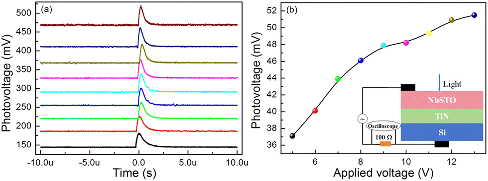 | ||
| Fig. 5 (a) Transient photovoltage responses at 248 nm with different applied voltage under 0.4 mW cm−2. (b) Photovoltage variation versus the applied voltage for the NbSTO/TiN/Si heterostructure. | ||
The optoelectronic properties of materials are closely related to their light absorption efficiency, photogenerated electron–hole pair separation dynamics, and the regulation of charge transport after separation. In the NbSTO/TiN/Si heterojunction, its excellent broadband optoelectronic characteristics stem from its band engineering. The electronic structure characteristics of each component provide the foundation for heterojunction design: the work function of TiN is significantly regulated by its composition, with an intrinsic work function of approximately −4.6 eV.35 However, Ti vacancies reduce the work function (e.g., a Ti vacancy content of 10% corresponds to approximately −4.3 eV, and it can increase to −3.2 eV when the Ti vacancy content reaches 60%), while N vacancies decrease it.36–38 Through analysis of Fig. 1d in this study, it was determined that the prepared TiN contains approximately 4% Ti vacancies; thus, the work function of TiN is reasonably speculated to range from −4.6 to −4.3 eV. The bandgap of NbSTO, as determined from Fig. 2, is approximately 3.58 eV. Silicon, with its well-known bandgap of about 1.05 eV and a conduction band minimum (CBM) at −4.05 eV.8,14,39 Based on these material properties, a band diagram of the NbSTO/TiN/Si heterojunction was constructed, as shown in Fig. 6. When the heterojunction is irradiated with 808 nm/532 nm lasers, since the bandgap of NbSTO is 3.58 eV, the photon energies of 808 nm (1.54 eV) and 532 nm (2.33 eV) lasers are insufficient to generate photogenerated carriers in NbSTO layer. In contrast, Si substrate, with a bandgap of 1.05 eV and a CBM at −4.05 eV, can absorb the laser photon energy, exciting valence band electrons to the conduction band and generating photogenerated electron–hole pairs. At the TiN/Si interface, the work function of TiN (−4.6∼−4.3 eV) differs from the CBM of Si (−4.05 eV), forming a built-in electric field directed from Si substrate to TiN layer. Under this field, photogenerated electrons migrate and accumulate in the Si substrate, while holes move toward the TiN layer. However, the two opposing potential barriers hinder the migration of photogenerated holes in the TiN layer, leading to hole accumulation near the barriers. As electrons continuously accumulate on the Si side, its potential decreases (becoming negatively charged), while the NbSTO layer, lacking carrier generation, becomes relatively positive due to the overall potential difference in the system. This results in a photovoltage between the NbSTO and Si terminals.
 | ||
| Fig. 6 Energy-band diagrams of the NbSTO/TiN/Si heterostructure. | ||
Additionally, under the same power density illumination, the significantly higher photovoltage generated by the 808 nm laser compared to the 532 nm laser can be attributed to the following synergistic mechanisms: (1) the localized surface plasmon resonance effect of the TiN thin film at 820 nm (confirmed in Fig. 2) significantly enhances infrared light field localization, promoting more carrier generation via the hot electron injection mechanism; (2) since the photon energy of 808 nm is closer to the bandgap of Si, it excites the intrinsic absorption of Si more efficiently than the 532 nm photon does, while reducing surface recombination losses caused by higher-energy photons. In contrast, under 248 nm ultraviolet pulsed laser irradiation, the photon energy (5.0 eV) exceeds the bandgap of NbSTO, making it the primary source of carrier generation, while Si absorbs negligible light. The built-in electric field at the NbSTO/TiN interface drives photogenerated electrons to accumulate in the NbSTO layer and holes to migrate toward the TiN layer. Although the built-in field at the TiN/Si interface still exists, the Si substrate does not generate significant carriers and merely acts as a charge conduction channel. Ultimately, electron accumulation in NbSTO lowers its potential relative to Si, creating a photovoltage with polarity opposite to that observed under 808 nm illumination. Therefore, the NbSTO/TiN/Si heterostructure achieves broadband spectral response through dual Schottky junction design and interfacial band engineering. In the Vis-IR region, the Si/TiN Schottky junction dominates carrier separation, which is further enhanced by the plasmonic resonance of TiN. In the UV region, the NbSTO/TiN Schottky junction drives efficient charge separation. Meanwhile, the TiN interlayer not only reduces lattice mismatch but also serves as a charge transport medium to optimize carrier transport. This synergistic multi-mechanism interaction enables the heterostructure to exhibit outstanding photoelectric performance across the ultraviolet to infrared spectral range.
Conclusions
In this work, we successfully fabricated the NbSTO/TiN/Si heteroepitaxial structures via pulsed laser deposition for broadband photodetection from UV to IR wavelengths. The TiN buffer layer not only reduced lattice mismatch between NbSTO and Si but also enhanced interfacial charge transport through its metallic properties and localized surface plasmon resonance effects. Photovoltaic characterization revealed superior performance under 808 nm and 365 nm illumination, with photovoltages reaching 193 mV and 100.2 mV, respectively, significantly outperforming the TiN/Si structures. The dual Schottky junction mechanism—where the Si/TiN junction dominated IR/visible response and the NbSTO/TiN junction facilitated UV carrier separation—ensured balanced photodetection. Additionally, the photoconductive effect under 248 nm pulsed light demonstrated bias-dependent responsivity, further validating the heterostructure's broadband response capability. Our work presents a reliable material design strategy for Si-based high-performance broadband photodetectors, providing a new approach with broad application prospects for their development.Experimental section
Fabrication of NbSTO/TiN/Si heteroepitaxial structure
The NbSTO/TiN/Si double heterojunction was epitaxially grown using a multi-target pulsed laser deposition system. N-type Si (100) wafers were used as substrates, which underwent standard wet chemical cleaning (with a final HF treatment) before being loaded into a vacuum chamber with a base pressure below 5 × 10⁻⁴ Pa. During fabrication, a KrF excimer laser (λ = 248 nm, τ = 20 ns) was employed to sequentially deposit TiN buffer layers and NbSTO (0.05 wt% Nb) films without breaking the vacuum. The 16 nm-thick TiN buffer layer was deposited at 800 °C with a laser pulse energy of 450 mJ and repetition rate of 4 Hz, followed by the deposition of a 50 nm-thick NbSTO film at 700 °C with adjusted laser parameters (250 mJ, 2 Hz). The TiN buffer layer serves dual purposes: (1) reducing the lattice mismatch between NbSTO and the Si substrate, and (2) suppressing the formation of silicon oxide interfacial layers during NbSTO deposition.40 After deposition, the samples underwent in situ annealing for 60 minutes. For comparison, the control sample consisting of only 16 nm TiN films on Si substrates was also prepared.Characterization
The crystalline properties of the samples were characterized by X-ray diffraction (XRD) using a Rigaku D/Max-Ra diffractometer with monochromatic Cu Kα radiation (λ = 1.54178 Å). The epitaxial quality of the thin films was examined by high resolution transmission electron microscopy (HRTEM) at 200 kV (Philips TECNAI F20), while the surface morphology and film uniformity were analyzed using atomic force microscopy (AFM, SPA-400 of SII). Compositional distribution was determined by Rutherford backscattering spectrometry (RBS, NEC 6SDH-2 model). UV-visible-infrared absorption spectra were measured with a Shimadzu UV-3101PC spectrophotometer. Electrical properties were evaluated by current–voltage (I–V) measurements under both dark and illuminated conditions using a Keithley 2400 source meter. For photoelectrical characterization, a Ti (10 nm)/Ag (300 nm) bilayer structure was adopted. Rectangular electrodes (15 mm × 3 mm each) were fabricated on both the film surface and the silicon substrate backside, with an interelectrode spacing of 8 mm. Subsequently, annealing was performed at 400 °C for 3 minutes in forming gas ambient to establish ohmic contacts. The photoresponse characteristics were measured using an 800 MHz oscilloscope, with illumination provided by an 808 nm semiconductor laser, 532 nm frequency-doubled Nd:YAG laser, a 365 nm mercury lamp, and a 248 nm KrF excimer laser. The light spot size was confined to an effective irradiation area of 78.9 mm2 using an optical slit. All measurements were performed at room temperature.Author contributions
Minghao Hu: conceptualization, data curation, investigation, methodology, software, writing – original draft; Tianyu Cai: conceptualization, data curation, formal analysis, investigation, methodology; Weiqiang Yang: formal analysis, investigation; Bin Yue: data curation, investigation; Anran Niu: data curation, investigation; Bingbing Li: data curation, investigation; Wenfeng Xiang: funding acquisition, resources, supervision, writing – review & editing. All the authors approved the final version.Conflicts of interest
There are no conflicts to declare.Data availability
The data that support the findings of this study are available from the corresponding author upon reasonable request.Acknowledgements
This work was supported by the National Natural Science Foundation of China (62075245).References
- Z. Li, T. Yan and X. Fang, Nat. Rev. Mater., 2023, 8, 587–603 CrossRef
.
- R. Zhang, G. Wang, Q. Zhang, S. Wang, X. Hu, L. Liu, S. Lv, W. Chen, X. Xu and L. Zhang, J. Mater. Chem. C, 2025, 13, 10972–10996 RSC
- S. Wei, B. Chen, J. Zhu, X. Wu, C. Zhang, D. W. Zhang, Q.-Q. Sun, L. Ji and S. Hu, ACS Appl. Electron. Mater., 2025, 7, 5069–5079 CrossRef CAS
- M. G. Uddin, S. Das, A. M. Shafi, L. Wang, X. Cui, F. Nigmatulin, F. Ahmed, A. C. Liapis, W. Cai, Z. Yang, H. Lipsanen, T. Hasan, H. H. Yoon and Z. Sun, Nat. Commun., 2024, 15, 571 CrossRef CAS PubMed
- I. Kim, R. J. Martins, J. Jang, T. Badloe, S. Khadir, H.-Y. Jung, H. Kim, J. Kim, P. Genevet and J. Rho, Nat. Nanotechnol., 2021, 16, 508–524 CrossRef CAS PubMed
- B. Li, Z. Shang and H. Zhou, J. Alloys Compd., 2025, 1010, 177177 CrossRef CAS
- N. Kumar, T. T. Nguyen, M. Patel, S. Kim and J. Kim, J. Alloys Compd., 2022, 898, 162788 CrossRef CAS
- K. Li, H. Chen, K. Ling, W. Li and X. Liu, J. Alloys Compd., 2023, 959, 170492 CrossRef CAS
- G. Chen, Y. Yu, Y. Shi, N. Li, W. Luo, L. Cao, A. J. Danner, A.-Q. Liu and X. Zhang, Laser Photon. Rev., 2022, 16, 2200117 CrossRef CAS
- J. Chen, C. Tan, G. Li, L. Chen, H. Zhang, S. Yin, M. Li, L. Li and G. Li, Small, 2021, 17, 2006496 CrossRef CAS PubMed
- Q. Huang, L. Tao, H. Zhu, W. Lin, J. Chen and Y. Fang, J. Mater. Sci.: Mater. Electron., 2025, 36, 401 CrossRef CAS
- J. Liu, S. Cristoloveanu and J. Wan, Phys. Status Solidi A, 2021, 218, 2000751 CrossRef CAS
- N. Ding, W. Xu, H. Liu, Y. Jing, Z. Wang, Y. Ji, J. Wu, L. Shao, G. Zhu and B. Dong, Light: Sci. Appl., 2024, 13, 289 CrossRef CAS PubMed
- C. Mao, F. Yao, D. Aleksandrov, F. Liu and W. Wu, ACS Appl. Mater. Interfaces, 2025, 17, 31230–31236 CrossRef CAS PubMed
- G. Yang, C. Zheng, Y. Zhu, X. Li, J. Huang, X. Xu, W. Liu, S. Cui and G. Pan, J. Alloys Compd., 2022, 921, 166097 CrossRef CAS
- N. Ding, W. Xu, D. Zhou, Y. Ji, Y. Wang, R. Sun, X. Bai, J. Zhou and H. Song, Nano Energy, 2020, 78, 105278 CrossRef CAS
- Z. He, S. Zhang, L. Zheng, Z. Liu, G. Zhang, H. Wu, B. Wang, Z. Liu, Z. Jin and G. Wang, IEEE Electron Device Lett., 2022, 43, 1818–1821 CAS
- H. Wu, Z. Liu, B. Wang, L. Zheng, S. Lian, J. Zhang, S. Zhang, G. Zhang, Z. Xue, S. Yang, X. Cheng, G. Ding, Z. Liu, C. Ye and G. Wang, ACS Photonics, 2024, 11, 1342–1351 CrossRef CAS
- W. Hu, H. Cong, W. Huang, Y. Huang, L. Chen, A. Pan and C. Xue, Light: Sci. Appl., 2019, 8, 106 CrossRef PubMed
- M. Zhang, L. Wang, L. Meng, X.-G. Wu, Q. Tan, Y. Chen, W. Liang, F. Jiang, Y. Cai and H. Zhong, Adv. Opt. Mater., 2018, 6, 1800077 CrossRef
- C. Liu, W. Wu, J. Liang and H. Zhou, Opt. Express, 2024, 32, 42793–42800 CrossRef CAS
- X. Chen, X. Yang, Q. Lou, Y. Tian, Z. Liu, C. Lv, Y. Chen, L. Dong and C.-X. Shan, Nano Res., 2023, 16, 1277–1285 CrossRef CAS
- S. H. Aleithan, U. Younis, Z. Alhashem and W. Ahmad, J. Alloys Compd., 2024, 1006, 176356 CrossRef CAS
- G. Y. Huang, Y. Hao, S. Q. Li, Y. D. Jia, J. C. Guo, H. Zhang and B. Wang, J. Phys. D: Appl. Phys., 2023, 56, 113001 CrossRef CAS
- F. Tian, S. Wu, X. Liu, B. Qiao, D. Pu, Z. Li, C. Chen, X. Cao, S. C. Bodepudi, M. A. Anwar, X. Wang, Y. Zhao, B. Yu, T. Hasan, H. Hu and Y. Xu, Sci. Sin. Inf., 2025, 68, 140405 Search PubMed
- C. Wang, H. Nan, Q. Wu, W. Wang, T. Zheng, Z. Ni, Z. Wu, X. Wan, Z. Cai, X. Gu and S. Xiao, ACS Appl. Mater. Interfaces, 2025, 17, 30019–30028 CrossRef PubMed
- J. Liu, C. Zhang, B. Ma, T. Yang, X. Gu, X. Wang, J. Zhang and C. Hu, Nano Energy, 2017, 38, 271–280 CrossRef CAS
- W. Xiang, C. Zhao, K. Liu, G. Zhang and K. Zhao, J. Alloys Compd., 2016, 658, 862–866 CrossRef CAS
- S. Liu, Y. Chen, W. Gao, W. Li, X. Yang, Z. Li, Z. Xiao, Y. Liu and Y. Wang, Adv. Mater., 2023, 35, 2303544 CrossRef CAS PubMed
- T. Ohsawa, T. Murakami, T. Hosaka, S. Ueda, T. Ishigaki and N. Ohashi, J. Phys. Chem. C, 2021, 125, 14836–14842 CrossRef CAS
- A. Kumar and J. Dho, Curr. Appl. Phys., 2013, 13, 768–774 CrossRef
- Z. Zarhri, A. D. Cano, O. Oubram, Y. Ziat and A. Bassam, Micro
Nanostruct., 2022, 166, 207223 CrossRef CAS
- M. Choi, A. B. Posadas, C. A. Rodriguez, A. O'Hara, H. Seinige, A. J. Kellock, M. M. Frank, M. Tsoi, S. Zollner, V. Narayanan and A. A. Demkov, J. Appl. Phys., 2014, 116, 043705 CrossRef
- P. Patsalas, N. Kalfagiannis, S. Kassavetis, G. Abadias, D. V. Bellas, C. Lekka and E. Lidorikis, Mater. Sci. Eng., R, 2018, 123, 1–55 CrossRef
- M. Alaloul and J. B. Khurgin, IEEE Photon. J., 2021, 13, 1–8 Search PubMed
- F. Fillot, T. Morel, S. Minoret, I. Matko, S. Maîtrejean, B. Guillaumot, B. Chenevier and T. Billon, Microelectron. Eng., 2005, 82, 248–253 CrossRef CAS
- S. Ishii, S. L. Shinde, W. Jevasuwan, N. Fukata and T. Nagao, ACS Photonics, 2016, 3, 1552–1557 CrossRef CAS
- M. Yuan, M. Wu, Y. Wen, X. Wang, B. Cui, J. Liu, Y. Wu, H. Dong, F. Lu, W.-H. Wang, P. Ren, S. Ye, H. Lu, R. Wang, Z. Ji and R. Huang, APL Electron. Dev., 2025, 1(1), 016107 CrossRef
- P. Guha, A. Ghosh, A. Sarkar, S. Mandal, S. K. Ray, D. K. Goswami and P. V. Satyam, Nanotechnology, 2018, 30(3), 035204 CrossRef PubMed
- W. F. Xiang, H. B. Lu, Z. H. Chen, X. B. Lu, M. He, H. Tian, Y. L. Zhou, C. R. Li and X. L. Ma, J. Cryst. Grow., 2004, 271, 165–170 CrossRef CAS
| This journal is © The Royal Society of Chemistry 2025 |