DOI:
10.1039/C8MH00590G
(Communication)
Mater. Horiz., 2018,
5, 961-968
A class of Pb-free double perovskite halide semiconductors with intrinsic ferromagnetism, large spin splitting and high Curie temperature†
Received
18th May 2018
, Accepted 23rd July 2018
First published on 24th July 2018
Abstract
Room-temperature ferromagnetic (FM) semiconductors are of vital importance for realizing advanced spintronic devices. The recent discovery of diluted ferromagnetism in Mn-doped CH3NH3PbI3 suggests hopes for developing halide perovskite based spintronics. However, the measured Curie temperature was usually below 15 K, which severely prohibits the Mn-doped CH3NH3PbI3 from being applied in room-temperature applications. In this work, instead of using the usual doping strategy, we present a new class of Pb-free FM halide semiconductors with double perovskite structures (Cs2GeMX6, transition metal M = V, Mn or Ni; X = Cl, Br or I), which possess spin splitting in a broad range of 0.06–1.00 eV and ultrahigh Curie temperature of 490–800 K. Furthermore, the Curie temperature can still be higher than room temperature under the lattice expansion effect. These excellent intrinsic properties are because of the large number of nearest neighboring magnetic ions and strong exchange coupling between the M 3d and GeX6 σs–p* orbitals. Our designed Pb-free FM halide semiconductors with double perovskite structures can be envisaged to develop into other highly dynamic research fields with vast implications for high-performance spin optoelectronics and spintronics.
Conceptual insights
As the Moore's law approaches the limit, spintronics has received intensive research interest due to its potential to revolutionize information technology. The utilization of spintronics requires the creation of a ferromagnetic semiconductor that can work at room temperature. Here, we introduce famous photovoltaic/optoelectronic material perovskite halides into the spintronics field. We present a series of intrinsic ferromagnetic semiconductors, namely double perovskite halides with a stable crystalline structure at room temperature. Furthermore, the ferromagnetic compounds are semiconductors with large spin splitting and high Curie temperature, which is crucial for extending the applications of perovskite halides in spintronics.
|
Introduction
Spintronics has demonstrated great potential in next-generation high speed and low power consumption information technology.1,2 However, it is still a major challenge to obtain 100% spin polarized carriers at room temperature (RT). Until now, a considerable amount of spintronic materials have been explored, such as europium chalcogenides (EuO, EuS),3–5 spinel (NiFe2O4, CoFe2O4),6,7 perovskite oxides (BiFeO3) and double perovskite oxides (Bi2CrOsO6),2,8–13 Heusler compounds (CoVTiAl, CoVZrAl)14 and layered Cr-based materials as well as the corresponding low-dimensional compounds (CrGeTe3 and CrI3).15–18 However, their small quantity of spin polarized carriers and low Curie temperature are two critical obstacles before realizing the corresponding RT spintronics.1 Therefore, two prerequisites should be fulfilled for realizing 100% spin polarized carriers at RT: (i) the electronic band structures should be nondegenerate with consequent large spin splitting; (ii) the Curie temperature (TC) should be at least higher than RT.1,19
Although pristine halide perovskites (ABX3, A = monovalent organic molecule or alkali metal, B = divalent carbon group cation and X = halogen anion) possess excellent optoelectronic properties, they usually exhibit no magnetism.20–29 Náfrádi et al. reported Mn-doped CH3NH3PbI3 with a weak magnetism, which suggests a promising route towards halide perovskite based spintronics.30 However, the small spin splitting of less than 0.2 eV and low Curie temperature of lower than 15 K in their devices should be greatly improved before obtaining RT operated spintronics. Also, their adopted doping strategy could lead to aggregation and secondary phase separation of dilute magnetic materials. In contrast, intrinsic ferromagnetic semiconductors without any assistance of a doping strategy should be highly desirable in spintronic applications. Double perovskite oxides have been widely used for spintronic applications due to their simple crystal structures and consequent facile modelling, the large number of members of their elemental family as well as their tunable electronic and magnetic properties.1 However, the magnetism of double perovskite halides (DPHs) has so far not been explored.
In this work, via first-principles calculations, we present a new class of Pb-free ferromagnetic (FM) DPHs with large spin splitting and ultrahigh TC. Twenty-four types of Pb-free DPHs, namely Cs2GeMX6 (M = Ti, V, Cr, Mn, Fe, Co, Ni or Cu and X = Cl, Br, or I), have been investigated in detail, and ten of them exhibit good structure stability. Among the ten materials, based on the analysis of magnetic ground states and electronic properties, Cs2GeMX6 with M = V and Mn are FM semiconductors, and five of the FM DPHs have large spin splitting. Other DPHs, Cs2GeMX6 (M = Ti and Cr), are antiferromagnetic (AFM) materials. Moreover, all the FM compounds have Curie temperatures higher than 490 K, which is because DPHs possess a large number of nearest neighboring magnetic ions z = 12 and the strong exchange coupling between the M 3d and GeX6 σs–p* orbitals. Furthermore, the TC cannot be less than room temperature. Combining the good stability, nontoxic properties and large spin splitting together with ultrahigh TC, Cs2GeMnX6 DPHs are promising candidates for spintronic applications.
Results and discussion
Crystallographic structures and magnetic ground states
Perovskites can usually exhibit four phases: cubic, tetragonal, orthorhombic and monoclinic. The cubic lattice is the most basic structure of perovskites, and the tetragonal lattice can be transferred to the cubic phase during the structure optimization. Moreover, the orthorhombic and monoclinic lattice can collapse in our simulation. Hence, we have mainly investigated the cubic lattice in this work. In cubic DPH A2BIBIIX6 structures, each unit cell of DPH equals a 2 × 2 × 2 single perovskite supercell, which contains four BIX6 octahedrons and four BIIX6 octahedrons. Two kinds of octahedrons alternately arrange along the three crystallographic axes, as shown in Fig. 1a. BI and BII atoms locate at the center of BIX6 and BIIX6 octahedrons, respectively. BI sites are occupied with the Ge element, because Ge-based perovskite halides have a similar formation energy to Pb-based perovskite halides, and both of them show better structure stability compared with Sn-based perovskite halides.31 For BII sites, transition metals are good candidates because of their unpaired d electrons, which usually lead to magnetism. The A sites locate at the octahedral interstice, which are filled with Cs ions. The reason for using Cs is that Cs can avoid the imposition of an arbitrary orientation for the organic group cation, and avoid the creation of a spontaneous polarization field in the organic group cations. The arbitrary orientation would increase the simulation difficulty, and the polarization field would affect the electronic properties. The optimized lattice constants a, and bond lengths lGe–X and lM–X are given in Table S1, ESI.†
 |
| | Fig. 1 (a) Crystalline structure of Cs2GeMX6. lGe–X and lM–X are the Ge–X and M–X bond length, respectively. (b) Schematic illustration of the constructed FM coupling state and three AFM coupling states. The adopted magnetic unit cell is a 2 × 2 × 2 double perovskite supercell. Here, we only present magnetic M-site atoms. The blue and red colors denote the spin-up and spin-down M atoms, respectively. | |
To calculate the magnetic ground states of Cs2GeMX6, a magnetic unit cell was used to estimate the system energy, as shown in Fig. 1b. In these structures, the magnetic unit cell is defined as a 2 × 2 × 2 double perovskite supercell. We firstly construct one FM coupling state and three AFM coupling states. However, according to space and energy analysis, the AFM-(100) state is the same as AFM-(110). In terms of the total energy, Cs2GeVX6, Cs2GeMnX6, and Cs2GeNiX6 are FM states, while Cs2GeTiX6, Cs2GeCrX6, Cs2GeFeX6 and Cs2GeCoX6 are AFM, and Cs2GeCuX6 is nonmagnetic (NM), respectively. We further analyzed the electron configuration of M ions. The result could explain the difference between the magnetic ground state of DPHs. From Ti to Ni, the d orbitals are occupied by unpaired d electrons, which lead to a magnetic moment in M atoms, thereby giving rise to FM or AFM states. However, the 3d orbitals of Cu are occupied by five electron pairs. Thus, no spin magnetic moments can be found in Cs2GeCuX6, endowing the NM ground state in Cu-based DPHs.
Structure stability
Stability is a very important property of new materials. Here, we examine the different stabilities of DPHs through simulations. Firstly, effective tolerance factor teff and octahedral factor μeff were used to evaluate the crystallographic stability. Most of the DPHs locate in the area of 0.44 < μeff < 0.90 and 0.81 < teff < 1.11, which indicates that they are crystallographically stable, as shown in Fig. 2a. The result also indicates that the cubic phase is the most suitable structure for our simulation, because perovskites tend to form the cubic phase when the tolerance factor teff is close to 1.32,33 Secondly, we constructed different arrangement configurations of Cs2GeMBr6. The energy analysis indicates that the alternative arrangement of GeBr6 and MBr6 octahedrons is the most energetically favorable configuration, as shown in Fig. 2b. It is worth mentioning that other thermodynamic metastable phases may exist at finite temperatures since their energy differences are very small. Furthermore, the kinetic stabilities of DPHs are confirmed by phonon spectra, as shown in Fig. 2c. We can find soft modes, which indicate instability, in the 0 K phonon spectra. However, these soft modes disappear when the temperature rises up to 300 K. This result shows that DPHs exhibit the stable cubic phase at RT. Meanwhile, we find that the longitudinal optic–transverse optic (LO–TO) branch splitting feature at the gamma point is missing, which is caused by the high symmetry of cubic phase double perovskite halides. Herein, we do not discuss this point because LO–TO splitting is governed by different physics. Finally, we check the decomposition processes through phase diagram analysis. Fig. 2d shows slices of the polyhedron for stable Cs2GeMnBr6 in chemical potential μCs = −4.0 eV. The complete data of phase diagram analysis are given in the ESI.† The gray regions in Fig. 2d can satisfy all chemical potential constraints, which means that high quality DPH samples without secondary competing phases can be realized in experiments. All results reveal that some DPHs are feasible in experiments.
 |
| | Fig. 2 (a) Distribution mapping of Cs2GeMX6 perovskites with different effective tolerance factors (teff) and octahedral factors (μeff). The stable region is highlighted by the cyan color. (b) Total energies of Cs2GeMnBr6 with different types of GeBr6 (in gray) + MnBr6 (in purple) motif arrangements. The lowest energy corresponding to configuration A was set to be zero. (c) Calculated phonon spectra at 0 K (left-hand side) and 300 K (right-hand side) of Cs2GeMnBr6. (d) Phase stability diagram analysis of double perovskite halides Cs2GeMnBr6. Only the slices at the chemical potential ΔμCs = −4.0 eV planes are shown here. The polygon region in gray represents thermodynamic stable conditions and each line corresponds to one competing phase. | |
Spin electronic properties
In order to understand the electronic and magnetic structures of all these systems, we analyzed the electronic configurations of AFM and FM DPHs, as shown in Fig. 3. Since the s electrons of the M atoms form bonds with the surrounding halogen atoms, only 3d electrons participate in orbital splitting in the octahedron crystal field and contribute to the magnetism. According to the crystal field theory, Hund's rule, the Pauli exclusion principle, and the Jahn–Teller (J–T) effect, the d orbitals could split into t2g and eg orbitals, and then further split into dxy, dyz and dzx and dx2−y2 and dz2. Only V with d3 configuration, high spin Mn with d5, and Ni with d8 can avoid J–T distortions and have more effective coupling with surrounding atoms. As a result, V-based, Mn-based, and Ni-based DPHs display FM states.
 |
| | Fig. 3 (a) Diagram of the electronic configurations of transition metal M 3d orbitals. Unevenly occupied 3d orbitals would induce the Jahn–Teller effect, thereby giving rise to further splitting of t2g and eg orbitals. (b) Spin density of FM state Cs2GeVBr6, Cs2GeMnBr6 and Cs2GeNiBr6, respectively. The isovalue is 0.014 e Å−3. | |
The spin densities of Cs2GeVBr6, Cs2GeMnBr6 and Cs2GeNiBr6 are shown in Fig. 4. The result clearly indicates that the magnetism origin is M 3d orbitals (3 fold-degenerated t2g for V, 3 fold-degenerated t2g and 2-fold degenerated eg for Mn and 2-fold degenerated eg for Ni), which is in good agreement with the above discussions.
 |
| | Fig. 4 Spin density of FM state Cs2GeVBr6, Cs2GeMnBr6 and Cs2GeNiBr6, respectively. The isovalue is 0.014 e Å−3. | |
Because the main features of the GGA + Ueff electronic properties are the same as HSE06 (see ESI†), we discuss their electronic structures by using GGA + Ueff methods. Considering the toxic nature of V-based DPHs and the instability of Ni-based DPHs, we only displayed the spin-polarized band structure to study the bandgaps and spin splitting of FM ground state DPHs. The related information of the spin-polarized band structure of all FM ground state DPHs is shown in Table 1 and Fig. S3 in the ESI.† In terms of band structures, Cs2GeMnX6 DPHs are half semiconductors (HSCs, M = V, and Mn). HSCs refer to the semiconductors in one spin channel, whereas they are insulators in the other spin channels. Their valence band (VB) and conduction band (CB) are spin split with the valence band maximum (VBM) and conduction band minimum (CBM) possessing the same spin channel.
Table 1 The spin splitting (denoted by ΔEVBM = EupVBM − EdownVBM and ΔECBM = EupCBM − EdownCBM, in eV), nearest and next nearest exchange parameters J1 and J2 (in meV), energy band gaps (Eg, in eV), and magnetic moments per magnetic atom (M, in μB) for halide double perovskites by using the GGA + Ueff method
|
|
ΔECBM |
ΔEVBM |
E
g
|
J
1
|
J
2
|
M
|
| Cs2GeVCl6 |
−0.40 |
1.00 |
2.26 |
−9.47 |
−1.37 |
3 |
| Cs2GeVBr6 |
−0.30 |
0.71 |
2.04 |
−8.53 |
−1.24 |
3 |
| Cs2GeVI6 |
−0.21 |
0.01 |
1.78 |
−7.40 |
−1.09 |
3 |
|
|
| Cs2GeMnCl6 |
−0.35 |
0.86 |
2.21 |
−8.56 |
−3.75 |
5 |
| Cs2GeMnBr6 |
−0.39 |
0.78 |
1.59 |
−7.76 |
−3.38 |
5 |
| Cs2GeMnI6 |
−0.43 |
0.20 |
1.05 |
−6.82 |
−2.99 |
5 |
|
|
| Cs2GeNiCl6 |
0.56 |
0.68 |
1.82 |
−6.15 |
−3.24 |
2 |
| Cs2GeNiBr6 |
0.32 |
0.48 |
1.37 |
−5.50 |
−2.89 |
2 |
| Cs2GeNiI6 |
0.09 |
0.06 |
0.97 |
−4.80 |
−2.52 |
2 |
For Mn-based DPHs, the compounds are ferromagnetic semiconductors with the VBM and CBM occupied by the spin-up carriers, as shown in Fig. 5. The CBM is mainly dominated by the spin-up Ge p orbitals, and the VBM derives from the antibonding of the Mn eg, Ge s, and X p orbitals. Cs2GeMnX6 (X = Cl, Br and I) has indirect bandgaps of 2.21 eV, 1.59 eV and 1.05 eV, respectively. As X changes from Cl, to Br, to I, the p orbital energy of X increases, leading to the lift of the VBM. The evolution of the VBM level accounts for the slightly decreasing profile of the band gap from 2.21 eV to 1.05 eV and ΔEVBM from 0.86 eV to 0.20 eV. Moreover, the splitting can reach up to 0.86 eV, 0.78 eV and 0.43 eV for Cs2GeMnCl6, Cs2GeMnBr6 and Cs2GeMnI6, respectively. The half semiconductors are also ideal spintronic materials due to the presence of large spin splitting.
 |
| | Fig. 5 Spin-polarized band structures of (a) Cs2GeMnCl6, (b) Cs2GeMnBr6 and (c) Cs2GeMnI6. Blue and red lines represent the spin-up and spin-down states, respectively. The width of the gray region represents the spin splitting value. | |
Curie temperature
We now turn to study the magnetic properties of these compounds at finite temperatures. There are several mechanisms for the occurrence of long-range FM order at finite temperatures: barriers due to the nearest-neighboring number z of magnetic ions, the exchange integral J between two magnetic ions, and other factors in experiments. Here, the nearest-neighboring number z = 12 in DPHs is two times as much as that in double perovskite oxides (DPOs). This means that if the exchange integral J is equal in two systems, the spin flip needs to cross a higher barrier in DPHs. Thus, a long-range FM order can be stabilized at higher temperatures. Since z = 12 is a constant in these systems, we will not discuss more on this parameter. Large exchange integral J is critical to stabilize the long-range FM order. The nearest and the next nearest exchange parameter J1 and J2 can be extracted from the energy difference of the magnetic unit cell in Fig. 1b by using eqn (1)–(3). The data of J1 and J2 are listed in Table 1. The negative and positive J represent FM and AFM coupling, respectively.| | | E(FM) = (192J1 + 96J2)|S|2 | (1) |
| | | E(AFM1) = (−64J1 + 96J2)|S|2 | (2) |
| |  | (4) |
Then, we can extract TC by performing the Ising model. In this model, the magnetic coupling Hamiltonian is expressed in eqn (4), in which the spin exchange parameter J1,2 is the nearest and the next nearest exchange parameter, and Si(j,k,l) is the total magnetic moment at site i (j, k, l). The Ising model is confirmed to provide good agreement with the experiments.14 To estimate the TC, we performed Monte Carlo (MC) simulation.8,11,34 Our MC simulation is based on a 20 × 20 × 20 supercell, and the average magnetic moment per unit cell was extracted after the system reached equilibrium. Fig. 6 displays the magnetic moment of the systems as a function of temperature variation. It is clear to see that with an increase of the temperature, the magnetic moment of the system shows a sudden decrease at a certain temperature. This phenomenon indicates there is a magnetic phase transition and this temperature is the TC. It can be seen that the TC values of Cs2GeMnCl6, Cs2GeMnBr6, Cs2GeMnI6, Cs2GeVCl6, Cs2GeVBr6, Cs2GeVI6, Cs2GeNiCl6, Cs2GeNiBr6, and Cs2GeNiI6 are measured to be 800 K, 720 K, 640 K, 730 K, 660 K, 580 K, 640 K, 560 K, and 490 K, respectively.
 |
| | Fig. 6 Variation of the total magnetic moment per formula unit of Cs2GeMX6 (M = V, Mn, or Ni, X = Cl, Br, or I) as a function of temperature. | |
From the above results, we know that DPHs can realize both semiconducting properties and high TC. In general, the semiconductor characteristic is incompatible with high TC. Why is the TC of semiconductor DPHs much higher than RT?
Here, we take Cs2GeMnCl6 as an example to clarify the semiconductor characteristic. Previous study shows that the CBM and VBM of CsMIVAX3 (MIVA = Ge, Sn and Pb; X = Cl, Br and I) and Cs2MIVAX6 are dominated by the MIVA p orbitals and MIVAX6 σs–p* orbitals, respectively. The MIVAX64− octahedron is the direct and main origin of semiconductor characteristics of CsMIVAX3 and Cs2MIVAX6.31 In these systems, semiconducting GeCl6 groups were inserted into transition metal ions. This configuration can seriously limit carrier movements, thereby leading to semiconducting properties in the compounds. Since the bridging GeCl64− group in our work was different compared with the single-atom anion in the traditional superexchange, we identify it as the quasi superexchange coupling. The DHP crystal can remain semiconducting despite the interaction being strong between magnetic ions and non-magnetic anions, because the octahedrons exhibit environment-independent semiconducting properties.
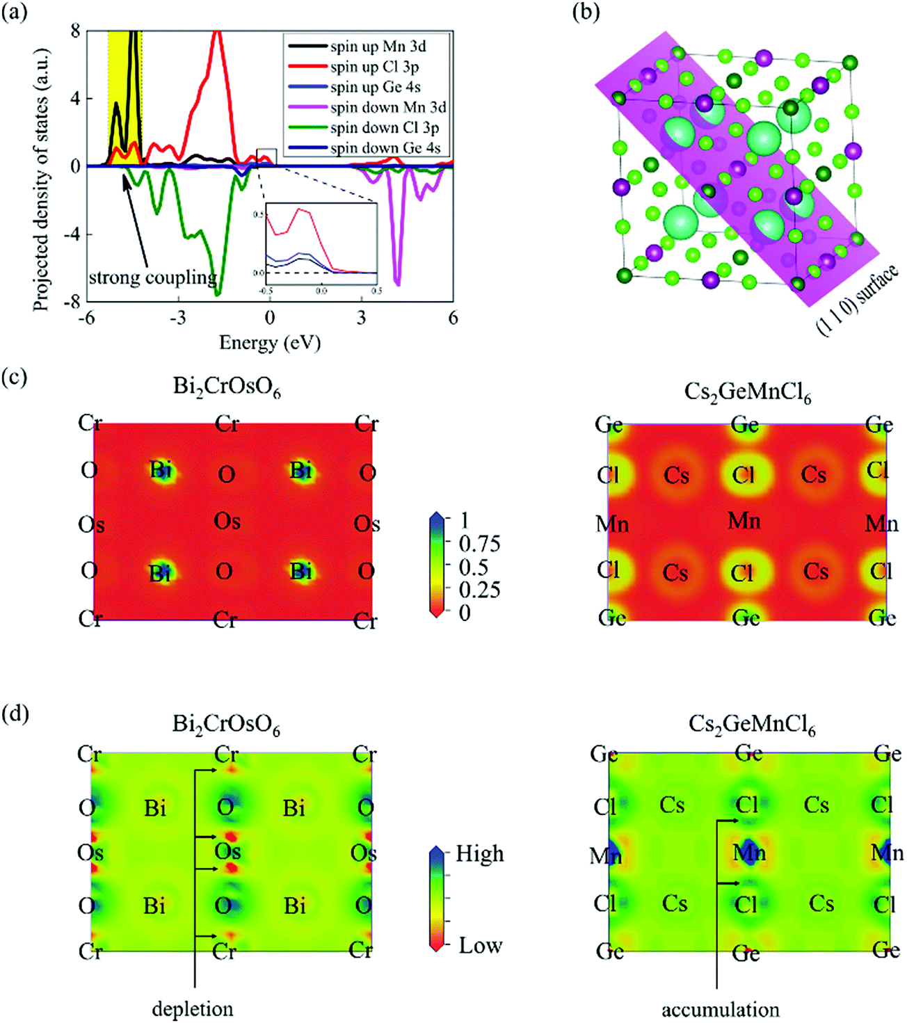
Then, we compared the difference between Cs2GeMnCl6 and Bi2CrOsO6 to study the origin of high TC in DPHs. Exchange parameters are related by the coupling style. Since the distance between two nearest neighbor transition metal ions is larger than 7.0 Å, the direct coupling between them should be negligible. The indirect exchange coupling through the GeX6 groups between two transition metal ions plays a majority role in ultrahigh TC. From Fig. 7a, we can find a strong coupling between Mn 3d and Cl 4p orbitals. Hence, the indirect coupling can be described as a 90° quasi-superexchange model between the Mn 3d and GeCl6 σs–p* orbitals, while the coupling model of DPOs is 180° superexchange of Cr(d)–O(p)–Os(d). The 90° superexchange interaction is more suitable for the ferromagnetic interaction compared to the 180° superexchange according to the Pauli exclusion principle. Exchange parameters are also determined by the overlap of charge distributions. Next, we calculated the electron location function (ELF) and deformation charge density (DCD) to analyse the indirect exchange coupling. The (110) plane was selected to analyse the ELF and DCD results because it contains four kinds of atoms in the quaternary compounds, as shown in Fig. 7b. Fig. 7c shows the ELF of two double perovskites, we observed that the maximum value locates at the Bi sites and the minimum value locates at the Cr/Os/O sites. In contrast, the maximum value and the minimum value are at the Ge/Cl and Cs/Mn sites in Cs2GeMnCl6. This evidence reveals that DPOs and DPHs have different bonding states. In other words, the iconicity of the M–GeX6–M bond is stronger than the M–O–M bond with an increased electron density at the GeX6 site than the O site. Fig. 7d shows the DCD of two kinds of double perovskites, we can see that there is charge depletion between the O and Os (Cr) atoms in Bi2CrOsO6. However, there is charge accumulation that can be found between Mn and the GeCl6 groups in Cs2GeMnCl6. The charge depletion in Bi2CrOsO6 gives rise to the weaker overlap of charge distribution in DPOs than that in DPHs, resulting in a weaker exchange coupling in Os–O–Cr. Hence, the TC of DPHs are much higher than Bi2CrOsO6 (201 K). Furthermore, the difference between the charge overlap cannot be used to clarify the bandgap. This is because the Bi atoms and Bi–O bonds affect significantly the Bi2CrOsO6 band structure, whereas the Cs atoms and Cs–Cl bonds do not have such effects.
 |
| | Fig. 7 (a) Orbital-projected density of states for Cs2GeMnCl6. All the Fermi levels are set to be zero. (b) The (110) plane (highlighted by purple) of the double perovskite structures, which contains all types of atoms. Maps of (c) the electron localization function (ELF) and (d) the deformation charge density for the DPO Bi2CrOsO6 and Cs2GeMnCl6 DPHs, respectively. | |
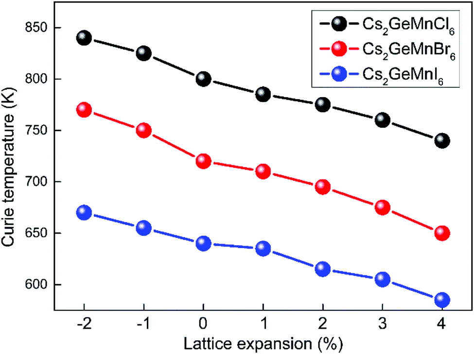
We extracted the TC by freezing the lattice constants in the above discussion. However, the lattice constant expansion (or contraction) is a common phenomenon, and a lot of factors can induce lattice constant change, such as interface lattice mismatch in devices and lattice thermal expansion. The lattice expansion could change the charge distribution, thereby affecting the exchange constant J. As a result, the result of TC could change. Considering the toxic effect of the V element and the instability of Cs2GeNiX6, we do not supplement the calculation of Cs2GeVX6 and Cs2GeNiX6. Here, we only calculate the strain effect of Cs2GeMnX6 on TC. In our calculation, the expansion ε is defined as
| |  | (5) |
where
a0 is the expansion lattice constant and
a is the equilibrium lattice constant. The negative value corresponds to the lattice contraction. The result is presented in
Fig. 8.
TC shows a monotone decrease with increasing
ε. With the lattice expansion, the overlap of charge distribution becomes weaker, which would make the exchange coupling less effective. As a result,
TC can decrease with the lattice expansion and can remain higher than RT at a reasonable expansion effect.
 |
| | Fig. 8 Calculated lattice expansion effect on the TC of Cs2GeMnX6. | |
Conclusions
In summary, via DFT calculations, we have presented a new class of semiconductor DPH Cs2GeMX6 with large spin splitting and high TC. The DPH Cs2GeMX6 (M = Ti, V, Cr, Mn, Fe, Co, Ni, or Cu) exhibits a cubic lattice with GeX6 and MX6 alternating along the three crystallographic axes. Based on the calculation of the octahedral factor μeff and tolerance factor teff, along with the analysis of phonon spectra and the phase diagram, we found that ten of the twenty-four designed compounds possess good structural stability. Importantly, seven of the nine FM ground state DPHs have spin splitting larger than 0.4 eV and TC in the range of 490–800 K. Moreover, the TC can remain much higher than room temperature under the lattice expansion effect. Combining the excellent structural stability, nontoxic properties, large spin splitting and high TC, Cs2GeMnX6 DPHs are the most ideal spintronic materials. Furthermore, we analyzed the origin of the semiconducting properties coupled with a high TC. The semiconducting properties are caused by the alternating arrangement of magnetic transition metal ions and semiconducting groups. Moreover, the large number of nearest neighboring magnetic ions and the strong exchange coupling between the M 3d and GeX6 σs–p* orbitals play a decisive role in the high TC. Also, the mechanism analysis of the semiconductor characteristics coupled with high TC could shed new light on the future design of advanced ferromagnetic semiconductors with tailored properties. In parallel with the current research into perovskite-based optoelectronics, our designed DPH semiconductors could open another intriguing route for the research of perovskite-based spintronics.
Conflicts of interest
There are no conflicts to declare.
Acknowledgements
This work was financially supported by the Fundamental Research Funds for the Central Universities (No. 30916015106), the National Basic Research Program of China (2014CB931702), the China Postdoctoral Science Foundation (AD41712) and the National Science Foundation for Distinguished Young Scholars of China (61725402). We thank Prof. Qiang Sun and Prof. Erjun Kan for fruitful discussions.
References
- X. Li and J. Yang, Natl. Sci. Rev., 2016, 3, 365–381 CrossRef
 .
.
- M.-R. Li, M. Retuerto, Z. Deng, P. W. Stephens, M. Croft, Q. Huang, H. Wu, X. Deng, G. Kotliar, J. Sánchez-Benítez, J. Hadermann, D. Walker and M. Greenblatt, Angew. Chem., Int. Ed., 2015, 54, 12069–12073 CrossRef PubMed .
- T. S. Santos and J. S. Moodera, Phys. Rev. B: Condens. Matter Mater. Phys., 2004, 69, 241203 CrossRef .
- J. Moodera, X. Hao, G. Gibson and R. Meservey, Phys. Rev. Lett., 1988, 61, 637 CrossRef PubMed .
- X. Hao, J. Moodera and R. Meservey, Phys. Rev. B: Condens. Matter Mater. Phys., 1990, 42, 8235 CrossRef .
- U. Lüders, A. Barthélémy, M. Bibes, K. Bouzehouane, S. Fusil, E. Jacquet, J. P. Contour, J. F. Bobo, J. Fontcuberta and A. Fert, Adv. Mater., 2006, 18, 1733–1736 CrossRef .
- U. Lüders, M. Bibes, K. Bouzehouane, E. Jacquet, J.-P. Contour, S. Fusil, J.-F. Bobo, J. Fontcuberta, A. Barthélémy and A. Fert, Appl. Phys. Lett., 2006, 88, 082505 CrossRef .
- S. Zhe-Wen and L. Bang-Gui, Chin. Phys. B, 2013, 22, 047506 CrossRef .
- X. Li, X. Wu, Z. Li and J. Yang, Phys. Rev. B: Condens. Matter Mater. Phys., 2015, 92, 125202 CrossRef .
- P. Ravindran, R. Vidya, A. Kjekshus, H. Fjellvåg and O. Eriksson, Phys. Rev. B: Condens. Matter Mater. Phys., 2006, 74, 224412 CrossRef .
- J. Wang, J. Meng and Z. Wu, J. Comput. Chem., 2011, 32, 3313–3318 CrossRef PubMed .
- E. Solana-Madruga, Á. M. Arévalo-López, A. J. Dos Santos-García, E. Urones-Garrote, D. Ávila-Brande, R. Sáez-Puche and J. P. Attfield, Angew. Chem., Int. Ed., 2016, 55, 9340–9344 CrossRef PubMed .
- A. M. Arévalo-López, G. M. McNally and J. P. Attfield, Angew. Chem., Int. Ed., 2015, 54, 12074–12077 CrossRef PubMed .
- E. Şaşıoğlu, L. Sandratskii, P. Bruno and I. Galanakis, Phys. Rev. B: Condens. Matter Mater. Phys., 2005, 72, 184415 CrossRef .
- C. Gong, L. Li, Z. Li, H. Ji, A. Stern, Y. Xia, T. Cao, W. Bao, C. Wang and Y. Wang, Nature, 2017, 546, 265–269 CrossRef PubMed .
- B. Huang, G. Clark, E. Navarro-Moratalla, D. R. Klein, R. Cheng, K. L. Seyler, D. Zhong, E. Schmidgall, M. A. McGuire, D. H. Cobden, W. Yao, D. Xiao, P. Jarillo-Herrero and X. Xu, Nature, 2017, 546, 270–273 CrossRef PubMed .
- X. Li and J. Yang, J. Mater. Chem. C, 2014, 2, 7071–7076 RSC .
- W.-B. Zhang, Q. Qu, P. Zhu and C.-H. Lam, J. Mater. Chem. C, 2015, 3, 12457–12468 RSC .
- K. Sato, L. Bergqvist, J. Kudrnovský, P. H. Dederichs, O. Eriksson, I. Turek, B. Sanyal, G. Bouzerar, H. Katayama-Yoshida and V. Dinh, Rev. Mod. Phys., 2010, 82, 1633 CrossRef .
- W.-J. Yin, J.-H. Yang, J. Kang, Y. Yan and S.-H. Wei, J. Mater. Chem. A, 2015, 3, 8926–8942 RSC .
- G. Giorgi and K. Yamashita, Chem. Lett., 2015, 44, 826–828 CrossRef .
- H.-J. Feng, T. R. Paudel, E. Y. Tsymbal and X. C. Zeng, J. Am. Chem. Soc., 2015, 137, 8227–8236 CrossRef PubMed .
- R. Dong, Y. Fang, J. Chae, J. Dai, Z. Xiao, Q. Dong, Y. Yuan, A. Centrone, X. C. Zeng and J. Huang, Adv. Mater., 2015, 27, 1912–1918 CrossRef PubMed .
- C. Huo, B. Cai, Z. Yuan, B. Ma and H. Zeng, Small Methods, 2017, 1, 1600018 CrossRef .
- X.-G. Zhao, J.-H. Yang, Y. Fu, D. Yang, Q. Xu, L. Yu, S.-H. Wei and L. Zhang, J. Am. Chem. Soc., 2017, 139, 2630–2638 CrossRef PubMed .
- X.-G. Zhao, D. Yang, Y. Sun, T. Li, L. Zhang, L. Yu and A. Zunger, J. Am. Chem. Soc., 2017, 139, 6718–6725 CrossRef PubMed .
- X. Liu, D. Yu, F. Cao, X. Li, J. Ji, J. Chen, X. Song and H. Zeng, Small, 2017, 13, 1700364 CrossRef PubMed .
- Z. Xiao, W. Meng, J. Wang, D. B. Mitzi and Y. Yan, Mater. Horiz., 2017, 4, 206–216 RSC .
- T. T. Tran, J. R. Panella, J. R. Chamorro, J. R. Morey and T. M. McQueen, Mater. Horiz., 2017, 4, 688–693 RSC .
- B. Náfrádi, P. Szirmai, M. Spina, H. Lee, O. Yazyev, A. Arakcheeva, D. Chernyshov, M. Gibert, L. Forró and E. Horváth, Nat. Commun., 2016, 7, 13406 CrossRef PubMed .
- P. P. Sun, Q. S. Li, L. N. Yang and Z. S. Li, Nanoscale, 2016, 8, 1503 RSC .
- Z. Li, M. Yang, J.-S. Park, S.-H. Wei, J. J. Berry and K. Zhu, Chem. Mater., 2016, 28, 284–292 CrossRef .
- M. R. Filip, G. E. Eperon, H. J. Snaith and F. Giustino, Nat. Commun., 2014, 5, 5757 CrossRef PubMed .
- F. Wu, C. Huang, H. Wu, C. Lee, K. Deng, E. Kan and P. Jena, Nano Lett., 2015, 15, 8277–8281 CrossRef PubMed .
Footnote |
| † Electronic supplementary information (ESI) available. CCDC 1858498–1858518. For ESI and crystallographic data in CIF or other electronic format see DOI: 10.1039/c8mh00590g |
|
| This journal is © The Royal Society of Chemistry 2018 |
Click here to see how this site uses Cookies. View our privacy policy here. 
 *a,
Xuhai
Liu
a,
Jinlong
Yang
*a,
Xuhai
Liu
a,
Jinlong
Yang